Abstract
In this study, a novel smart efficiency tracking (SET) algorithm for GaN-based LLC resonant converter for quick battery charging of light electric vehicles is proposed. Conventional frequency modulation (FM) method, single pulse width modulation method (S-PWM) and discontinuous operation mode method (DOM) are used to track the converter efficiency which varies for different loading conditions during the battery charging process. First, the charging modes are explained to define the efficiency variation clearly. Then, the theoretical background of GaN-based LLC resonant converter is presented and the details of design study are given. Third, the principles of three different switching control strategies, the modeling study and the simulation results are put forward. Finally, the details of the implementation of three different switching strategies are presented for the validation of the study. Furthermore, the implementation of the design and its impact on battery charging are discussed. The proposed efficiency tracking method is validated with a 20% efficiency increase for the low loading conditions of GaN-based LLC converter.
1. Introduction
In this paper, a smart efficiency tracking algorithm of GaN-based LLC resonant converter for quick charging of light electric vehicle batteries is proposed. Conventional frequency modulation (FM) method, S-PWM method and discontinuous operation mode method (DOM) principles are used to track the GaN-based LLC resonant converter efficiency throughout the whole cycle of the battery charging process, including constant current charging, i.e., fast charging, and constant voltage charging, i.e., slow charging.
With the increasing mobility and impact of improvements in electric and hybrid electric vehicles, research on battery problems becomes important and urgent. Battery issues such as life cycle, charge and health estimation are addressed with new methods and technologies. On the other hand, fast or quick charging is essential to make electric vehicles more desirable. Nowadays, long charging times seem to be the number one reason for the fading tendency to use more electric vehicles. Solutions for shorter charging times lie in more powerful charging supplies and high efficiency power electronic circuits. Researchers are pursuing the design of smaller and lighter charging circuits with exceptionally high efficiencies. So, fast or quick charging of batteries, especially Li-Ion batteries, is an eventual target for today’s power electronic circuit designers. New methods or novel circuit topologies are proposed continuously for improving fast charging process. In that effort, the LLC resonant converters have a special place due to their high power densities, higher efficiencies, small size and lighter structures. Because of their unique features, they are capable of transferring DC power with the highest possible efficiency in both directions, i.e., grid-to-battery and battery-to-grid [1,2].
Bidirectional power flow capability, high efficiency, high power density, high gain and galvanic isolation features of the dual active bridge PWM converter and LLC/CLLC resonant converter make those topologies the most convenient solutions for battery charging systems. There are many previous and ongoing pieces of academic research on those topologies [3,4]. Comparison of these two topologies over their advantages and disadvantages is one of the most discussed topics for academic researchers [5,6].
The dual active bridge converter has a simple design and can be easily controlled by a conventional PWM duty cycle method [7]. Both LLC and CLLC resonant converters are controlled by frequency modulation, so the design details of the two converters are mostly identical to each other except their resonant tank circuit [8,9]. Design details of both LLC and CLLC resonant converters are handled step by step in design guidelines of semiconducter manufacturers [10]. Smart grids and automotive applications are the main usage areas of LLC and CLLC resonant converters [11,12]. There are different types of studies on LLC resonant converters in the literature, such as matrix converter topologies which combine power factor correction (PFC) rectifier and LLC resonant converters [13].
Generally, battery voltage differs in a wide range during the charging process. There is a substantial amount of academic research on modifying circuit topology or control of the LLC resonant converters by adding auxiliary components to increase the converter efficiency [14,15]. As an example, the high efficiency operation of the LLC resonant converter can be satisfied by tracking the converter efficiency with the help of the perturb and observe method [16,17].
The low loss GaN switching components implementation is another way to increase the efficiency of DAB and LLC converters. The comparison of GaN and SiC switching components has been one of the most popular power electronics topics in recent years [6,7,9,18,19].
Synchronous rectification increases the efficiency of LLC resonant converters by driving the gates of secondary side switching components when the negative current flows through the switches, i.e., through their body diodes. Drive timing of the secondary side switching components is adjusted according to drain-source voltage (V) measurement or drain-source current (I) measurement [20,21]. There are also some studies on modulating the switching frequency of LLC converters by using synchronous rectification [22].
The most efficient operating point of the LLC converter is that the resonant current is purely sinusoidal. To satisfy the high efficiency operation of the LLC resonant converter in full range of battery voltage, the input voltage (V) is altered to follow the battery voltage when the LLC resonant converter operates in resonance continuously [19,23,24]. Using different PFC topologies and replacing resonant converter with DC/DC topologies by implementing the variable DC link voltage strategy are also mentioned in literature [25,26].
Low-load condition occurs with the decrease in battery charging current. Low or light loading is detected by measurement of average input current or monitoring the control signal voltage [27,28]. Decision of the control method type is handled accordingly.
Magnetizing current of the LLC resonant converter causes an extra power loss during the low-load operation. Circulation current is decreased by adjusting the dead-time between switching signals of two phase legs of primary full bridge to provide the high efficiency operation point. There is also some literature about this method [29,30]. The Light-load condition of the LLC resonant converter is the main focus of the research about phase-shift control [31,32].
Burst mode or DOM is one of the most convenient operation methods of DC/DC converters and there are several pieces of research about burst mode operation [28]. On-time and off-time optimization studies are important to observe the output voltage and current of the converter [33,34]. Off-on transition of the LLC resonant converter is also a critical issue for controlling the inrush current of the converter to increase the efficiency [35].
Combining two or three operation methods of the LLC resonant converter is another preferred topic to examine high efficiency operation. Dead-time control and discontinuous operation modes are used together to propose a new hybrid control technique [36]. Another well-known technique is the frequency modulation technique which is used in a wide operation range of LLC resonant converters and dead-time control is used under low load condition of battery charging process [37].
In the study, a new method which is dedicated to obtain the highest available efficiency is implemented for a novel switch (GaN) LLC converter. The novel approach tracks the converter efficiency for varying loading conditions during fast battery charging. The aim of the studied algorithm is to monitor the efficiency and to keep or alter the operation mode of the converter according to the monitored efficiency and loading condition. Three different operation modes are implemented to achieve the highest possible efficiency. The proposed smart efficiency tracking algorithm can be defined as a “monitor-and-change” scheme. Thus, during the whole charging process the efficiency of the converter can be kept at the highest value.
2. LLC Resonant Converter as a Battery Charger
Due to the advantages, such as high efficiency, high power density, low switch stress, wide range output regulation and relatively easy-to-control features, LLC converters are widely preferred in isolated battery charging applications.
Nowadays, fast battery charging systems and onboard chargers for electric vehicles mostly rely on LLC resonant converters due to their high efficiency and high power performances. Besides the mentioned superiorities, for low output power levels at low output current, i.e., higher switching frequencies, output voltage regulation becomes difficult and efficiency is reduced dramatically. The conventional battery charging characteristics via an LLC converter are shown in Figure 1. Due to varying ambient conditions and therefore charging durations, the time span is given as per unit in which unit time symbolizes the end of the charging process. During constant current charging, battery voltage increases almost linearly at the beginning, and efficiency increases due to closing to the nominal (rated) operation point of the converter. The output voltage of the converter is controlled to keep the charging current under the rising voltage. However, the state of charge (SoC) of the battery reaches 80% approximately and then the charging procedure is changed and shifted to a constant voltage region, wherein the charging current diminishes due to the total transferred charge to battery. For providing a decaying current, the output voltage of the LLC converter is reduced as well. To decrease output voltage, switching frequency of LLC converter is increased, when charging process nears to its end, wherein the efficiency of LLC converter also reduces substantially.
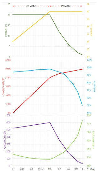
Figure 1.
Battery charge profile of LLC resonant converter.
Efficiency peaks when the output power is at its maximum as expected, whereas it is diminished due to the increased switching frequency. As is seen in Figure 1, the efficiency of the LLC converter is below 75% at a quarter of the total charging time. When the total charging process is considered, the efficiency variation implies a substantial amount of energy loss. On the other side, when the frequency is increased, the operation point of the converter moves to the off-resonance region. However, the essential requirement is to provide higher efficiencies at the light loading conditions which cover an important portion of the battery charging process, and is the aim of this study.
So the fundamental idea underlying the presented study is to obtain the highest possible efficiency for the overall operation region of the LLC converter during battery charging.
3. Topology and Design
3.1. Proposed Topology and Operation Intervals
In this study, the conventional full-bridge LLC resonant converter topology is used by implementing GaN power transistors shown in Figure 2. The fast charging process is conceived for the battery pack of a light electric vehicle so that it can be implemented in the laboratory environment. At the secondary side, another bridge topology which enables synchronous and bidirectional operations is applied for rectification. An LLC transformer links the primary and secondary sides and provides a non-ideal inductance amount to fulfill the resonant operation. The resonant tank can be considered as a harmonic filter tuned by the varying switching frequency.
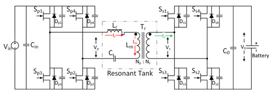
Figure 2.
LLC resonant converter topology.
In Figure 3, the six operation intervals of the LLC converter and their related waveforms are shown. Each operation interval has an impact on the overall performance of the converter.
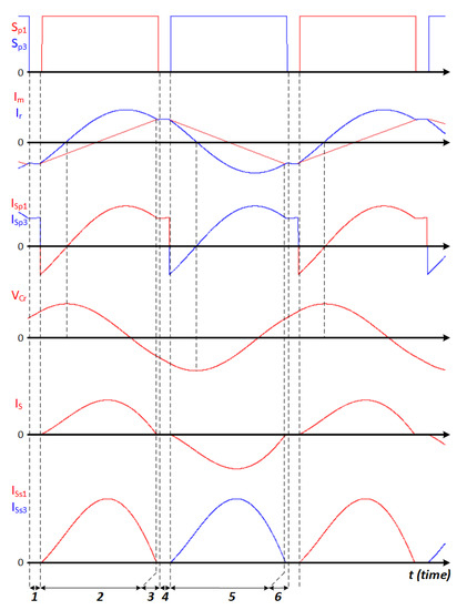
Figure 3.
Waveforms of LLC resonant converter and six (6) intervals of operation.
Interval-1 covers the dead-time for the transistors and there is no power transfer to the secondary during that operation interval. The primary current charges the terminal capacities of S and S whilst the capacities of S and S are discharged. After that charging and discharging process, the primary current finds its path through D and D and provides zero voltage switching (ZVS) operation. Figure A1 shows the power transfer during Interval-1.
In Interval-2, S and S switches are turned on and the power flow through the transformer is shown in Figure A2. The primary current is forced to commutate from negative to positive by applied positive voltage. Meanwhile, D and D are on at the secondary side to provide the load DC voltage. The DC voltage applied to the primary side causes an alleged linearly rising magnetizing current through L. Via C and L, the electrical resonance phenomenon occurs and provokes a sinusoidal current through the primary winding. When the magnetizing current exceeds the winding current, the power transfer is halted and Interval-2 ends.
At Interval-3, the secondary current, I, is not contributing to the output filter capacitor charging whilst the power transfer is ended by the termination of the current ringing, i.e., resonance. The primary current, now equal to the magnetizing current, continues to rise until S and Sare turned off, and the operation interval is ended with that termination. The power flow for Interval-3 is given in Figure A3.
Interval-4 covers the dead-time for the pair of S and S and for that interval there is no power transfer as it is shown in Figure A4. The primary current charges the terminal capacities of S and S whilst the capacities of S and S are discharged. After the charging and discharging process, the primary current is directed to the path of D and D and the ZVS operation is satisfied.
For Interval-5, the pair of S and S is turned on and power is transferred to the secondary. Due to the negative applied voltage to the transformer primary, the current is forced to shift from positive to negative. Basically, Interval-5 is the counterpart of Interval-2 for S and S transistors, and the power flow can be seen in Figure A5.
At Interval-6, because of the tendency of the ringing primary current, the sinusoidal current falls below the magnetizing current, such that the magnetizing current now gains dominance. The current rises to zero until S and S go to off-state. Due to soft decaying of the secondary current, D and D also become extinct softly. The interval ends by turning off S and S The power flow is given in Figure A6.
3.2. Design
Because of the complicated impedance circuit of the LLC resonant converter, the resonant operation is determined by two operation conditions which are depicted by two resonance frequencies. The first operation is characterized by infinite load resistance which coincides with no-load or open circuit operation and the resonant frequency f is given by Equation (1). The second resonant frequency f is for zero load resistance which shows short circuit operation and is given by Equation (2).
Theoretically, the first frequency is used for light loading conditions and the second one is for heavy loading conditions. However, mostly it is not practical to operate the circuit around the first frequency because of the low impedance value causing a high current demand. The voltage gain of LLC resonant converter is given by Equation (3).
The normalized frequency is defined as the ratio of switching frequency to resonance frequency, as given in Equation (4).
, the normalized inductance is given in Equation (5).
The quality factor of the converter depends on the loading and is given in Equation (6).
LLC resonant converter gain equation is given in Equation (7).
The quality factor is found as 1.8 for maximum loading conditions and 0.2 for minimum loading conditions.
The normalized inductance L is found as 26, which is quite high for conventional LLC converters. However, this value enables wider gain change with off-resonance operation, which is bringing a more versatile converter for dedicated battery charging applications.
According to the mentioned parameters, the gain characteristics of the converter can be obtained as the function of switching frequency, as it is seen in Figure 4: the fixed gain for varying loading at the resonance frequency.
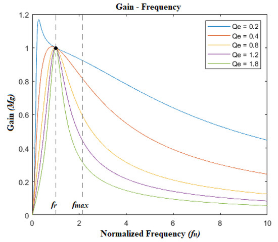
Figure 4.
Gain vs. frequency curves of LLC resonant converter.
The basic parameters of the designed LLC converter are presented in Table 1.

Table 1.
Design parameters of LLC resonant converter.
The gate voltage V of GaN switching elements shall be around +6 V DC and −3 V DC. In this paper, the gate drive circuit of GaN devices are designed as shown in Figure 5 by using application note [40] from GaN System Inc. Half-bridge switching power circuit is constructed and printed circuit board (PCB) drawing is prepared by considering the application note [41].
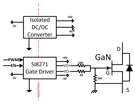
Figure 5.
Gate drive block diagram of a GaN device.
Application note [42] is examined and PCB production, soldering of GaN devices to the board is completed accordingly.
3.3. Transformer Design
The transformer is the most essential element of LLC resonant converter and directly affects the operation of the converter. The design is quite different than conventional designs. To provide an inductance for resonant operation, the transformer is intentionally designed to be imperfect by creating extra leakage inductance and small magnetizing inductance, such that the equivalent inductance of transformer contributes to resonant operation. Thus, separating primary and secondary windings and adding a substantial air gap to the ferromagnetic core are essential requirements for the transformer.
A special ferromagnetic core selection is made [43] and the transformer is designed according to the following criterion.
WA, P, D, K and B are the product of window area and core area, output power, current density, topology constant of core and maximum magnetic flux density, respectively. The number of turns of primary and secondary are calculated from the application of Faraday’s law to square wave primary voltage.
N, V, A, f, N, V are the primary winding turn, input voltage, cross section area, frequency, secondary winding turn and output voltage, respectively. The air gap length added to ferromagnetic core is calculated using the following equations.
L, A, L are the air gap length, required inductance factor and magnetizing inductance, respectively. The calculated parameters of the designed LLC resonant converter transformer is presented in Table 2.
Table 2.
Calculated parameters of designed LLC resonant converter transformer.
The principal transformer structure is given in Figure 6. Litz-wire is preferred in winding design to overcome the problems of skin and proximity effects.
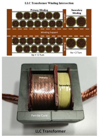
Figure 6.
Winding design of LLC resonant converter transformer.
4. Simulation Study and Experimental Work
In this paper, the conventional frequency modulation method, single pulse PWM method and discontinuous mode operation method have been used for improving GaN-based LLC resonant converter efficiency during whole battery charging process.
The simulation model of the LLC resonant converter, which is built in PSIM 64-bit version 9.0, is given in Figure 7. The parameters which are used in the model are presented in Table 1.
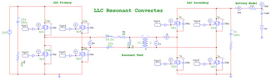
Figure 7.
Simulation model of LLC resonant converter.
To obtain switching signals, a voltage controlled oscillator sub-model is formed as shown in Figure 8.
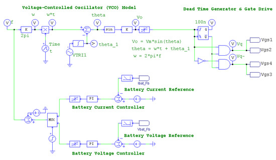
Figure 8.
Voltage controlled oscillator sub-model for LLC resonant converter simulation.
Figure 9 shows the experimental setup specially designed for the study.
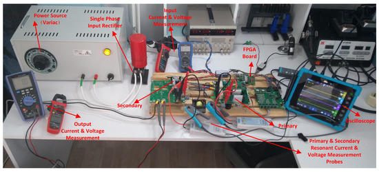
Figure 9.
Experimental setup.
The block diagram of the experimental setup is given in Figure 10.
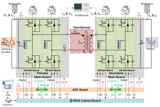
Figure 10.
Block diagrams of the experimental setup.
The input DC-link voltage is obtained from a variable AC transformer and a bridge rectifier. The resonance tank current is captured by a 2 MHz bandwidth isolated current probe and the voltages are measured by 100 MHz 4-channel oscilloscope via 2 kV differential voltage probes.
4.1. Conventional Frequency Modulation (FM) Operation Mode
In Figure 11, the simulation results including the primary current and voltage, battery current and voltage are given while the resonance operation implies nearly pure sinusoidal current and full-load. The experimental results for the same full-load operation condition in which primary current is sinusoidal are given in Figure 12.
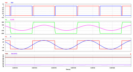
Figure 11.
LLC resonant converter FM simulation V = 29.4 V, I = 20 A, f = 218 kHz.
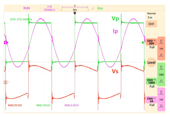
Figure 12.
LLC resonant converter FM experimental results V = 29.4 V, I = 20 A, f = 218 kHz.
The resonant operation is accomplished at 218 kHz switching frequency which is defined by the modeling study and the available transformer inductance and resonant capacitor values.
The voltage and current of the transformer primary and the battery voltage and current are given in Figure 13 for the simulation study of a 3 A charging current, which indicates partial loading at 270 kHz switching frequency. Figure 14 shows the experimental measurements of the voltage and current of the transformer primary and the battery voltage and current for the 3 A charging current at 270 kHz switching frequency.
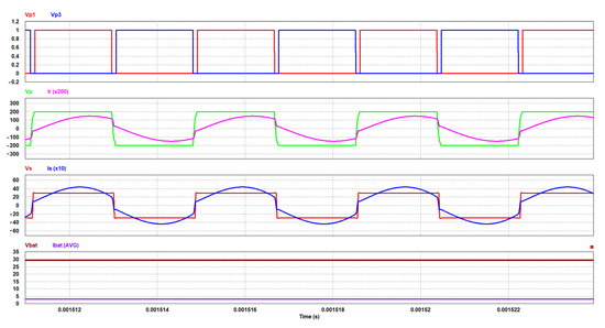
Figure 13.
LLC resonant converter FM simulation V = 29.4 V, I = 3 A, f = 270 kHz.
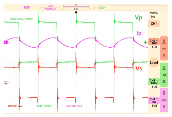
Figure 14.
LLC resonant converter FM experimental results V = 29.4 V, I = 3 A, f = 270 kHz.
The experimental efficiency data obtained by various loading conditions are presented in Table 3. As expected, for the light loading conditions, i.e., reduced charging current, the converter efficiency also inevitably decreases.
Table 3.
Conventional frequency modulation (FM) efficiency data.
4.2. Single Pulse Width Modulation (S-PWM) Operation Mode
In Figure 15, the simulation results, including the primary current and voltage, battery current and voltage, are given for 75% duty ratio at the resonance frequency, while the charging current is lower than 3 A. The experimental results for the same 75% duty ratio operation while the charging load is light, i.e., the charging current is below 3 A, are given in Figure 16. As it can be seen in the given figures, the primary current tends to be discontinuous because of light loading and canceled magnetizing current.
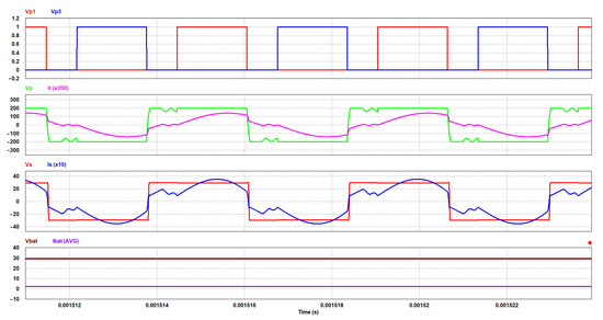
Figure 15.
LLC resonant converter S-PWM simulation V = 29.4 V, I = 2.3 A, f = 218 kHz, 75% S-PWM duty.
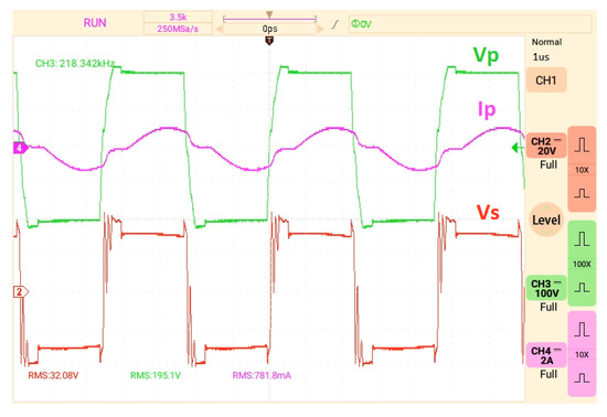
Figure 16.
LLC resonant converter S-PWM experimental result V = 29.4 V, I = 2.3 A, f = 218 kHz, 75% S-PWM duty.
The experimental efficiency data obtained by different loading conditions are presented in Table 4. The efficiency decreases for the duty ratios lower than 75%. Therefore, the operations for the duty ratios not exceeding 75% must be avoided due to the abrupt efficiency fall.
Table 4.
S-PWM operation mode efficiency data.
4.3. Discontinuous Operation Mode (DOM)
During the discontinuous operation, the primary current at the resonance frequency is let to flow for a certain number of periods, and then the current flow is halted for another number of periods and the operation is repeated cyclically. So, this process can be described as an intermittent current operation at resonance. Thus, another duty ratio which is different from conventional PWM is defined. Sometimes this type of control is called the integral control. The important point is to monitor the output voltage and current; if the charging voltage drops below a predetermined voltage level, another number of primary current periods are provided for keeping the output voltage almost constant. This operation is similar to the burst operation in switch-mode power supplies.
In Figure 17, the simulation results including the primary current and voltage and the battery current and voltage are given for 25% DOM duty ratio which coincides with a charging current below 2 A. The experimental results for the same operation are given in Figure 18.
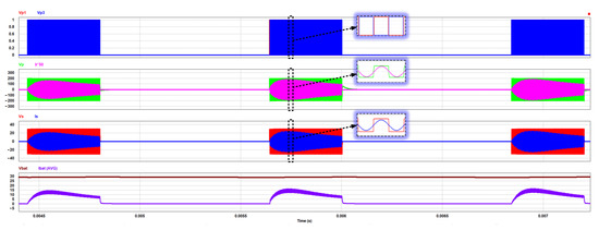
Figure 17.
LLC resonant converter DOM simulation V = 29.4 V, I < 2 A, f = 218 kHz, 25% DOM duty.
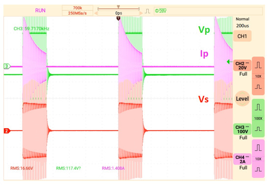
Figure 18.
LLC resonant converter DOM experimental results V = 29.4 V, I < 2 A, f = 218 kHz, 25% DOM duty.
The experimental efficiency data set is given in Table 5 for DOM. As it can be seen, the efficiency remains in the 84–88% interval for low DOM duty ratios. As a rule of thumb, for the charging currents not exceeding 2 A, DOM is used effectively. The problem with the DOM operation is to monitor and control the output voltage effectively. Only the output current is controlled to overcome any output transient. Even the resonant switching implies high dynamics, the overall operation of circuit has slower dynamics. So, the inrush current during DOM is not causing any harm or high transients at the output port. However, for large power LLC converters and small value output capacitors, an effective inrush current control may be required.
Table 5.
DOM efficiency data.
5. Proposed Algorithm
By analyzing the results given in Table 3, Table 4 and Table 5 with different switching modes, single PWM and DOM modes are evaluated as advantageous for the charging currents below 3 A. For the charging currents of 3 A and below, the efficiency of the LLC resonant converter is lower than 75%, as shown in Figure 1. By means of single PWM and DOM switching strategies, the efficiency is kept over 80%, as it is given in Figure 19. For the constant current charging mode, the LLC resonant converter is run at the conventional resonance operation which enables the maximum charging power. To keep the charging current at 20 A, the switching frequency is altered from 250 kHz down to 218 kHz. Then, for shifting to constant voltage charging, the switching frequency is increased to obtain the lower charging currents and the voltage control starts with a charging current of 4 A, and the efficiency is reduced to 85%.
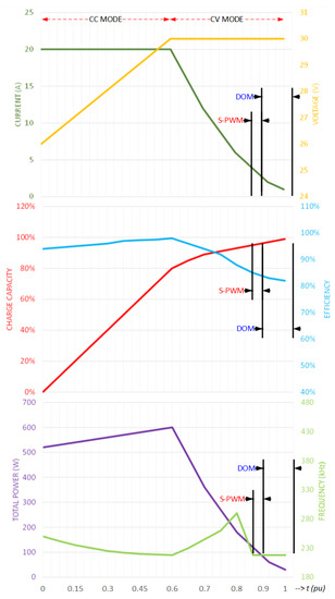
Figure 19.
Battery charge profile of LLC resonant converter with addition of the S-PWM and DOM.
While the current is between 2 A and 4 A, the S-PWM operation mode is applied between 100% to 75% S-PWM duty by setting the switching frequency to a fixed frequency of 218 kHz. If a lower charging current is requested, the switching frequency is kept at 218 kHz and the DOM control is started.
For charging currents under 2 A, the full DOM is employed. By means of that operation, the battery is fully charged without decreasing the charging efficiency to a level lower than 80%. The achieved improvement of efficiency via S-PWM and DOM is presented in Figure 20. Especially for low charging currents, a 20% increase in efficiency is obtained.
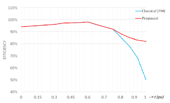
Figure 20.
Efficiency comparison of classical vs proposed methods.
An algorithm is developed for maximum available efficiency to shift among the operation modes as it is shown in Figure 21. In the flowchart, first it is checked whether constant voltage charging or constant current charging is necessary, then according to the battery charging current level, S-PWM or DOM is selected for optimum charging efficiency.
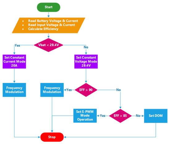
Figure 21.
One cycle flowchart of proposed algorithm.
6. Conclusions and Future Aspects
In this study, an algorithm for transition among the operation modes of an LLC resonant converter during battery charging is proposed. As it is shown in Figure 20, a maximum 25% increase can be obtained for low power charging operation, which is a challenging operation mode for resonant converters in general. The transition mechanism among the three different operation modes is simple and easy to implement.
The S-PWM operation is useful only for a narrow operation region. If the duty ratio is less than 75% in a half period, a substantial efficiency loss is occurred due to the resonance operation between the magnetizing inductance and resonant tank capacitor.
In DOM operation, the emerging inrush current at each switching start causes extra loss in efficiency. In the planned future studies, the DOM operation will be analyzed further and an adaptive frequency modulation will be used to reduce the inrush current for optimal efficiency operation.
As a result of pursuing a wide operation range of efficiency, a multi-mode switching method and control techniques are applied for shifting among the mentioned modes and explained by simulation and experimental results. A maximum 25% increase in efficiency can be provided, which is quite high for efficiency-critical applications such as battery charging.
Author Contributions
Conceptualization, E.Ç. and O.U.; methodology, E.Ç. and O.U.; software, E.Ç.; validation, E.Ç.; formal analysis, E.Ç. and O.U.; investigation, E.Ç. and O.U.; resources, E.Ç.; data curation, E.Ç.; writing—original draft preparation, E.Ç.; writing—review and editing, O.U.; visualization, E.Ç.; supervision, O.U.; project administration, O.U.; funding acquisition, E.Ç. and O.U. All authors have read and agreed to the published version of the manuscript.
Funding
This research received no external funding and the APC was jointly funded by both authors.
Institutional Review Board Statement
Not applicable.
Informed Consent Statement
Not applicable.
Data Availability Statement
Not applicable.
Conflicts of Interest
The authors declare no conflict of interest.
Appendix A
Active components of the LLC resonant converter topology according to intervals (1 to 6) are shown below.
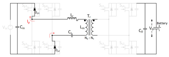
Figure A1.
LLC resonant converter topology interval-1.
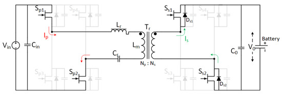
Figure A2.
LLC resonant converter topology interval-2.
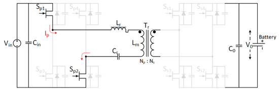
Figure A3.
LLC resonant converter topology interval-3.
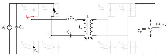
Figure A4.
LLC resonant converter topology interval-4.
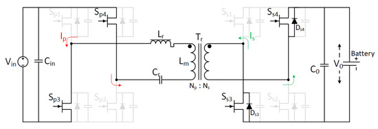
Figure A5.
LLC resonant converter topology interval-5.
Figure A6.
LLC resonant converter topology interval-6.
References
- Li, G.; Huang, J.; Zhang, W.; Tong, X.; Xiao, J.; Hai, M.K.L. High-efficiency Oriented Control Method of Bidirectional CLLC Resonant DC/DC Converter for Energy Storage System. In Proceedings of the 15th IEEE Conference on Industrial Electronics and Applications (ICIEA), Kristiansand, Norway, 9–13 November 2020; pp. 1254–1258. [Google Scholar] [CrossRef]
- Piasecki, S.; Zaleski, J.; Jasinski, M.; Bachman, S.; Turzyński, M. Analysis of AC/DC/DC Converter Modules for Direct Current Fast-Charging Applications. Energies 2021, 14, 6369. [Google Scholar] [CrossRef]
- Pavlović, Z.; Oliver, J.A.; Alou, P.; Garcia, Ó.; Cobos, J.A. Bidirectional Dual Active Bridge Series Resonant Converter with Pulse Modulation. In Proceedings of the 27th Annual IEEE Applied Power Electronics Conference and Exposition (APEC), Orlando, FL, USA, 5–9 February 2012; pp. 503–508. [Google Scholar] [CrossRef]
- Hillers, A.; Christen, D.; Biela, J. Design of a Highly Efficient Bidirectional Isolated LLC Resonant Converter. In Proceedings of the 15th International Power Electronics and Motion Control Conference (EPE/PEMC), Novi Sad, Serbia, 4–6 September 2012; pp. DS2b.13-1–DS2b.13-8. [Google Scholar] [CrossRef]
- He, P.; Khaligh, A. Comprehensive Analyses and Comparison of 1kW Isolated DC-DC Converters for Bidirectional EV Charging Systems. IEEE Trans. Transp. Electrif. 2017, 3, 147–156. [Google Scholar] [CrossRef]
- Qi, F.; Wang, Z.; Wu, Y. 650V GaN Based 3.3 kW Bi-Directional DC-DC Converter for High Efficiency Battery Charger with Wide Battery Voltage Range. In Proceedings of the IEEE Applied Power Electronics Conference and Exposition (APEC), Anaheim, CA, USA, 17–21 March 2019; pp. 359–364. [Google Scholar] [CrossRef]
- Costinett, D.; Nguyen, H.; Zane, R.; Maksimovic, D. GaN-FET Based Dual Active Bridge DC-DC Converter. In Proceedings of the 26th IEEE Applied Power Electronics Conference and Exposition (APEC), Forth Worth, TX, USA, 6–11 March 2011; pp. 1425–1432. [Google Scholar] [CrossRef]
- Yan, Y.H.; Chang, Y.N.; Peng, Z.X. Design of a Bidirectional CL3C Full-Bridge Resonant Converter for Battery Energy Storage Systems. Energies 2022, 15, 412. [Google Scholar] [CrossRef]
- Liu, G.; Li, D.; Jang, Y.; Zhang, J. Over 300kHz GaN Device Based Resonant Bidirectional DCDC Converter With Integrated Magnetics. In Proceedings of the IEEE Applied Power Electronics Conference and Exposition (APEC), Long Beach, CA, USA, 20–24 March 2016; pp. 595–600. [Google Scholar] [CrossRef]
- Choi, H. Analysis and Design of LLC Resonant Converter with Integrated Transformer. In Proceedings of the 22nd Annual IEEE Applied Power Electronics Conference and Exposition (APEC), Anaheim, CA, USA, 25 February–1 March 2007; pp. 1630–1635. [Google Scholar] [CrossRef]
- Gerekial, W.G. Bi-Directional Power Converters for Smart Grids. Master’s Thesis, Norwegian University of Science and Technology Department of Electric Power Engineering, Trondheim, Norway, June 2014. [Google Scholar]
- Henke, M. Analysis and Design of Resonant dc/dc Converters for Automotive Applications. Master’s Thesis, Institut für Elektrische Maschinen, Antriebe und Bahnen, TU Braunschweig, Braunschweig, Germany, June 2014. [Google Scholar]
- Thrimawithana, D.J.; Madawala, U.K.; Twiname, R.; Vilathgamuwa, D.M. A Novel Matrix Converter based Resonant Dual Active Bridge for V2G Applications. In Proceedings of the 10th International Power & Energy Conference (IPEC), Ho Chi Minh City, Vietnam, 12–14 December 2012; pp. 503–508. [Google Scholar] [CrossRef]
- Kim, E.S.; Oh, J.S.; Kim, M.J.; Lee, J.H.; Woo, J.W.; Jeon, Y.S. Enhancing Efficiency in Bidirectional Resonant DC-DC Converter. In Proceedings of the IEEE Applied Power Electronics Conference and Exposition (APEC), New Orleans, LA, USA, 15–19 March 2020; pp. 2230–2235. [Google Scholar] [CrossRef]
- Lu, J.; Tong, X.; Zeng, J.; Shen, M.; Yin, J. Efficiency Optimization Design of L-LLC Resonant Bidirectional DC-DC Converter. Energies 2021, 14, 3123. [Google Scholar] [CrossRef]
- Abu-qahouq, J.A.; Mao, H.; Al-atrash, H.J.; Batarseh, I. Maximum Efficiency Point Tracking (MEPT) Method and Digital Dead Time Control Implementation. IEEE Trans. Power Electron. 2006, 21, 1273–1281. [Google Scholar] [CrossRef]
- Väisxaxnen, V.; Hiltunen, J. Maximum Efficiency Point Tracking Algorithm for Dual Active Bridge Converters. In Proceedings of the IEEE Energy Conversion Congress and Exposition (ECCE), Montreal, QC, Canada, 20–24 September 2015; pp. 623–629. [Google Scholar] [CrossRef]
- Domb, M. High power density, high efficiency 380v to 52v LLC converter utilizing E-Mode GaN switches. In Proceedings of the PCIM Europe 2016; International Exhibition and Conference for Power Electronics, Intelligent Motion, Renewable Energy and Energy Management, Nuremberg, Germany, 10–12 May 2016; pp. 1–7. [Google Scholar]
- Ammar, A.M.; Ali, K.; Rogers, D.J. A Bidirectional GaN-Based CLLC Converter for Plug-In Electric Vehicles On-Board Chargers. In Proceedings of the IECON 46th Annual Conference of the IEEE Industrial Electronics Society, Singapore, 18–21 October 2020; pp. 1129–1135. [Google Scholar] [CrossRef]
- Zhang, Z.; Liu, C.; Si, Y.; Liu, Y.; Lei, Q. Investigation of Adaptive Synchronous Rectifier (SR) Driving Scheme for LLC/CLLC Resonant Converter in EV On-Board Chargers. In Proceedings of the IEEE Applied Power Electronics Conference and Exposition (APEC), New Orleans, LA, USA, 15–19 March 2020; pp. 2185–2191. [Google Scholar] [CrossRef]
- Feng, W.; Huang, D.; Mattavelli, P.; Fu, D.; Lee, F.C. Digital Implementation of Driving Scheme for Synchronous Rectification in LLC Resonant Converter. In Proceedings of the IEEE Energy Conversion Congress and Exposition, Atlanta, GA, USA, 12–16 September 2010; pp. 256–263. [Google Scholar] [CrossRef]
- Feng, W.; Mattavelli, P.; Lee, F.C. Pulsewidth Locked Loop (PWLL) for Automatic Resonant Frequency Tracking in LLC DC–DC Transformer (LLC-DCX). IEEE Trans. Power Electron. 2013, 28, 1862–1869. [Google Scholar] [CrossRef]
- Wang, H.; Dusmez, S.; Khaligh, A. A Novel Approach to Design EV Battery Chargers Using SEPIC PFC Stage and Optimal Operating Point Tracking Technique for LLC Converter. In Proceedings of the IEEE Applied Power Electronics Conference and Exposition, Fort Worth, TX, USA, 16–20 March 2014; pp. 1683–1689. [Google Scholar] [CrossRef]
- Wang, H.; Dusmez, S.; Khaligh, A. Maximum Efficiency Point Tracking Technique for LLC-Based PEV Chargers Through Variable DC Link Control. IEEE Trans. Ind. Electron. 2014, 61, 6041–6049. [Google Scholar] [CrossRef]
- Liu, C.; Wang, J.; Colombage, K.; Gould, C.; Sen, B. A CLLC Resonant Converter Based Bidirectional EV Charger with Maximum Efficiency Tracking. In Proceedings of the 8th IET International Conference on Power Electronics, Machines and Drives, Glasgow, UK, 19–21 April 2016; pp. 1–6. [Google Scholar] [CrossRef]
- Strzalkowski, B. Autonomous method of maximum power efficiency tracking for PFC- and DC/DC-converter system. In Proceedings of the International Exhibition and Conference for Power Electronics, Intelligent Motion, Renewable Energy and Energy Management, Nuremberg, Germany, 19–20 May 2015; pp. 1–4. [Google Scholar]
- Chen, J.; Sato, T.; Yano, K.; Shiroyama, H.; Owa, M.; Yamadaya, M. An Average Input Current Sensing Method of LLC Resonant Converters for Automatic Burst Mode Control. IEEE Trans. Power Electron. 2017, 32, 3263–3272. [Google Scholar] [CrossRef]
- Yang, C.H.; Liang, T.J.; Chen, K.H.; Li, J.S.; Lee, J.S. LLC Resonant Converter Controller with Novel Light Load Control. In Proceedings of the International Power Electronics and Application Conference and Exposition, Shanghai, China, 5–8 November 2014; pp. 131–135. [Google Scholar] [CrossRef]
- Ibanez, F.; Echeverria, J.M.; Fontan, L. Novel technique for bidirectional series-resonant DC/DC converter in discontinuous mode. IET Power Electron. 2013, 6, 1019–1028. [Google Scholar] [CrossRef]
- Hua, W.; Wu, H.; Yu, Z.; Xing, Y.; Sun, K. A Phase-Shift Modulation Strategy for a Bidirectional CLLC Resonant Converter. In Proceedings of the 10th International Conference on Power Electronics Ecce Asia, Busan, Korea, 27–30 May 2019; pp. 1–6. [Google Scholar] [CrossRef]
- Kim, J.H.; Kim, C.E.; Kim, J.K.; Lee, J.B.; Moon, G.W. Analysis on Load-Adaptive Phase-Shift Control for High Efficiency Full-Bridge LLC Resonant Converter Under Light-Load Conditions. IEEE Trans. Power Electron. 2016, 31, 4942–4955. [Google Scholar] [CrossRef]
- Zhu, T.; Zhuo, F.; Zhao, F.; Wang, F.; Yi, H.; Zhao, T. Optimization of Extended Phase-Shift Control for Full-Bridge CLLC Resonant Converter With Improved Light-Load Efficiency. IEEE Trans. Power Electron. 2020, 35, 11129–11142. [Google Scholar] [CrossRef]
- Chen, Y.C.; Liang, T.J.; Tseng, W.J.; Lee, J.Y.; Yang, L.S. Design and Implementation of LLC Resonant Converter with High Efficiency at Light Load Condition. In Proceedings of the 2nd International Symposium on Power Electronics for Distributed Generation Systems, Hefei, China, 16–18 June 2010; pp. 538–542. [Google Scholar] [CrossRef]
- Feng, W.; Lee, F.C.; Mattavelli, P.; Huang, D.; Prasantanakorn, C. LLC Resonant Converter Burst Mode Control with Constant Burst Time and Optimal Switching Pattern. In Proceedings of the 26th Annual IEEE Applied Power Electronics Conference and Exposition (APEC), Fort Worth, TX, USA, 6–11 March 2011; pp. 6–12. [Google Scholar] [CrossRef]
- Feng, W.; Lee, F.C.; Mattavelli, P. Optimal Trajectory Control of Burst Mode for LLC Resonant Converter. IEEE Trans. Power Electron. 2013, 28, 457–466. [Google Scholar] [CrossRef]
- Shi, L.; Liu, B.; Duan, S. Burst-Mode and Phase-Shift Hybrid Control Method of LLC Converters for Wide Output Range Applications. IEEE Trans. Ind. Electron. 2020, 67, 1013–1023. [Google Scholar] [CrossRef]
- Narli, J.; Tafti, H.D.; Farivar, G.G.; Pou, J.; Nguyen, B.X.; Hai, K.L. Control Scheme for LLC Resonant Converter with Improved Performance Under Light Loads and Wide Input-Output Voltage Variation. In Proceedings of the IEEE Energy Conversion Congress & Expo (ECCE), Baltimore, MD, USA, 29 September–3 October 2019; pp. 1605–1608. [Google Scholar] [CrossRef]
- GaN Systems–GS66508t Datasheet. Available online: https://gansystems.com/gan-transistors/gs66508t/ (accessed on 27 February 2022).
- GaN Systems–GS61008t Datasheet. Available online: https://gansystems.com/gan-transistors/gs61008t/ (accessed on 27 February 2022).
- GaN Systems–Gate Driver Circuit Design with GaN E-HEMTs (GN012). Available online: https://gansystems.com/wp-content/uploads/2021/07/GN012_Gate-Driver-Design-with-GaN-E-HEMTs_210720.pdf (accessed on 27 February 2022).
- GaN Systems–PCB Layout Considerations with GaN E-HEMTs (GN009). Available online: https://gansystems.com/wp-content/uploads/2021/07/GN009-PCB-Layout-Considerations-with-GaN-E-HEMTs_20210720.pdf (accessed on 27 February 2022).
- GaN Systems–Soldering Recommendations for GaNPX® and PDFN Packaged Devices (GN011). Available online: https://gansystems.com/wp-content/uploads/2021/09/GN011_Soldering-Recommendations-for-GaNPX%C2%AE-and-PDFN-Packaged-Devices-Rev-210917.pdf (accessed on 27 February 2022).
- Magnetics–Magnetics Ferrite Cores Transformer Design. Available online: https://www.mag-inc.com/Media/Magnetics/File-Library/Product%20Literature/Ferrite%20Literature/Magnetics-Ferrite-Catalog-2017.pdf?ext=.pdf (accessed on 27 February 2022).
Publisher’s Note: MDPI stays neutral with regard to jurisdictional claims in published maps and institutional affiliations. |
© 2022 by the authors. Licensee MDPI, Basel, Switzerland. This article is an open access article distributed under the terms and conditions of the Creative Commons Attribution (CC BY) license (https://creativecommons.org/licenses/by/4.0/).