Article

Miniaturized Distributed Generation for a Micro Smart Grid Simulator

Department of Electronic Engineering, Namseoul University, 91, Daehak-ro, Seonghwan-eup, Seobuk-gu, Cheonan-si 31020, Chungcheongnam-do, Korea
*
Author to whom correspondence should be addressed.
Energies 2022, 15(4), 1511; https://doi.org/10.3390/en15041511
Submission received: 22 December 2021 / Revised: 6 February 2022 / Accepted: 14 February 2022 / Published: 17 February 2022

Abstract

:
In this paper, a miniaturization method is proposed for developing micro distributed generation for a micro smart grid simulator. The micro smart grid simulator is a fault simulator that was built to test and verify the new operation control algorithms for smart grids in the laboratory and has a size downscaled to one-thousandth of that of an actual smart grid. The micro distributed generation was designed in a multi-layered structure (dimension: 13 × 20 cm2), in which each function is implemented in several layers, to satisfy the size requirements. Next, the grid synchronization and PQ control algorithms required for the distributed generation were developed. A three-phase 19 V power system was built, and a 19 V–7.5 W three-phase micro distributed generation was realized through experimental verification. In addition, by verifying the effectiveness through grid synchronization and 7.5 W PQ control experiments, it was confirmed that the micro distributed generation based on the proposed miniaturization method can be implemented in a micro smart grid simulator.

1. Introduction

Power systems are rapidly evolving into smart grids (SGs) that combine a digital communication network, which enables bidirectional communication between electricity producers and consumers, with power grids installed with distributed generation (DG) systems that maximize the efficiency of energy use. Several algorithms have been proposed for the protection and control of power grids with tree structures [1,2].
However, these algorithms cannot be applied directly, because the SGs, equipped with DG systems, exhibit different fault phenomena than those occurring in the existing power grids. In particular, the fault phenomena depend on the number of installed DG systems and their location. To solve this problem, new algorithms for protection and control of SGs have been proposed [3,4,5]. Unlike the protection and control algorithms, which use unidirectional communication, for existing power grids, the algorithms for SGs can utilize bidirectional communication between power facilities, including protection devices (PDs) and DGs. This makes the protection and control algorithms highly complex and difficult to implement. Accordingly, to apply the proposed algorithms to an actual SG, reliability must be ensured through sufficient and diverse fault analysis and tests performed on the SG.
Firstly, the developed algorithms are modelled and simulated via a software-based simulation approach. In this approach, the power system is modeled using software tools such as EMTP-RV [6,7] or PSCAD/EMTDC [8], and the overall performance is verified by modeling the proposed algorithm and then applying it to the system model. Although this approach is easy to apply in the laboratory, it is difficult to guarantee reliability unless the dynamic characteristics of the system are perfectly modeled by the best experts. Furthermore, it is impossible to test the power control device to which the algorithm is applied, directly. Additionally, testing the algorithm using the communication function of the SG is impractical. Secondly, a hardware-based approach can be considered. Although this method is used to assess the reliability of a system, it cannot be applied, because of a huge spreading effect that is observed when applied on a large-scale actual system. Therefore, a demonstration test site is required. However, the scale and configuration of the demonstration test site are significantly limited by the high costs and length of time required to construct such a demonstration test site. Given that the system voltage is high (23 kV) and has a limited configuration, it is difficult to satisfy the various special system configuration conditions required by new algorithms for SGs. Moreover, it is impossible for researchers to conduct experimental tests freely because of the accompanied risks, which may arise when such a system is operated by an operator who does not have expertise. Recently, hardware in the loop system has received significant attention [9,10] because of its hybrid approach, in which the performance of the new algorithms can be tested by providing input/output (IO) signals, from a modeled system based on a real time digital simulator (RTDS) to a hardware device developed through IO interfaces.
However, this approach is also likely to experience the same problems as the software approach mentioned before because the RTDS generates system dynamics based on software tools. To overcome this problem, a laboratory test environment is required to perform stable testing of the reliability of a power control device to which a new algorithm is applied under real-time voltage and current signals obtaining from the electrical dynamics of an actual SG. Additionally, a two-way communication test environment is required to test a new control strategy based on the bidirectional communication of the SG as well.
To date, several studies on miniaturization of systems or devices have been conducted in the fields of electronic devices [11,12], aerospace engineering [13], optics [14], and mechanics [15]. The miniaturization of sensors, computers, electric motors, microphones, medical devices, and robots has provided significantly innovative and successful solutions. In the biomedical field, a micro total analysis system, known as a “lab on a chip”, is proposed to reduce space and energy. Such a system is portable and integrates several processes that are performed in the laboratory to analyze and evaluate the samples and miniaturize them into a single device [16,17]. Furthermore, several successful research results have also been presented in the field of robotics based on miniaturized sensors and activators [18,19]. Recently, several studies on miniaturization in the power grids have been demonstrated [20,21]. Especially Ko (2018) [20], who proposed a new and efficient downscaling method for the miniaturization of SGs and presented the design results of a micro SG simulator based on the proposed method. This proposed micro SG simulator has a size that is one thousandth that of the SG, allowing free and safe experimentation with the new operation control algorithms in the laboratory. Ko et al. [21] proposed a miniaturized PD, known as a micro PD, to meet the specifications of the micro SG simulator. This micro PD plays the same roles as those of the circuit breaker (CB) and recloser or section switches on the micro SG simulator. However, the micro DG that plays the role of DG in the micro SG simulator, which is essential in verifying the control algorithms of the SG experimentally, remains hitherto unexplored. Several researchers proposed grid connection methodologies of DG for SG [22,23,24]; however, they cannot be applied directly to the micro SG simulator because of the large differences in the size and power levels of the DG systems. To realize this new method, a miniaturization method that can downscale the size and power levels to that of a micro SG simulator needs to be developed. In particular, whether or not control algorithms such as the grid synchronization and PQ control algorithms, applied to the SGs, are effective even at the micro SG simulator level should be verified. Such a verification would allow us to conversely infer that the control algorithms verified in the micro SG simulator have the same validity when applied to the SG.
Accordingly, herein, a miniaturization method for developing a micro DG that plays the role of DG in the micro SG simulator is proposed. In this study, first, the micro DG system was designed with a multi-layer structure, in which each function is implemented in several layers to satisfy the size requirements. Second, the grid synchronization and PQ control algorithms, required for the DG, were developed based on the DQ transformation. Third, the effectiveness of the developed algorithm was verified through EMTP modeling and simulation. Fourth, a three-phase 19 V power system was experimentally built, and based on this, one micro DG system was developed through experimental verification. Finally, through grid synchronization and PQ control experiments, it was verified that the micro DG based on the proposed miniaturization method could be applied as a DG of the micro SG simulator. Simultaneously, the dynamic electrical characteristics were analyzed during the connection operation to verify that the micro DG on the micro SG simulator shows the same electrical characteristics as those of the DGs of the SG.

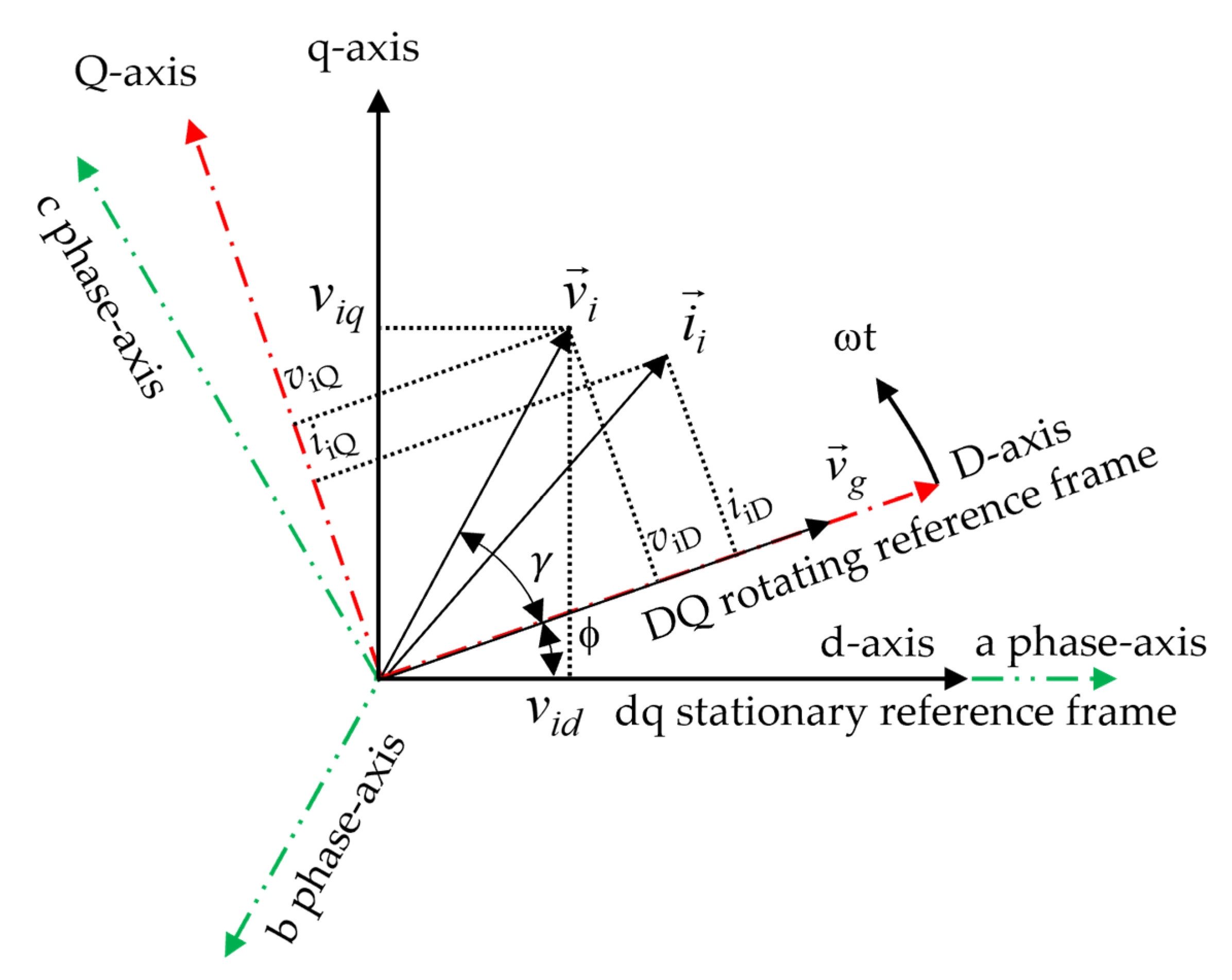
2. Equivalent Model of Smart Grid Connected with DG

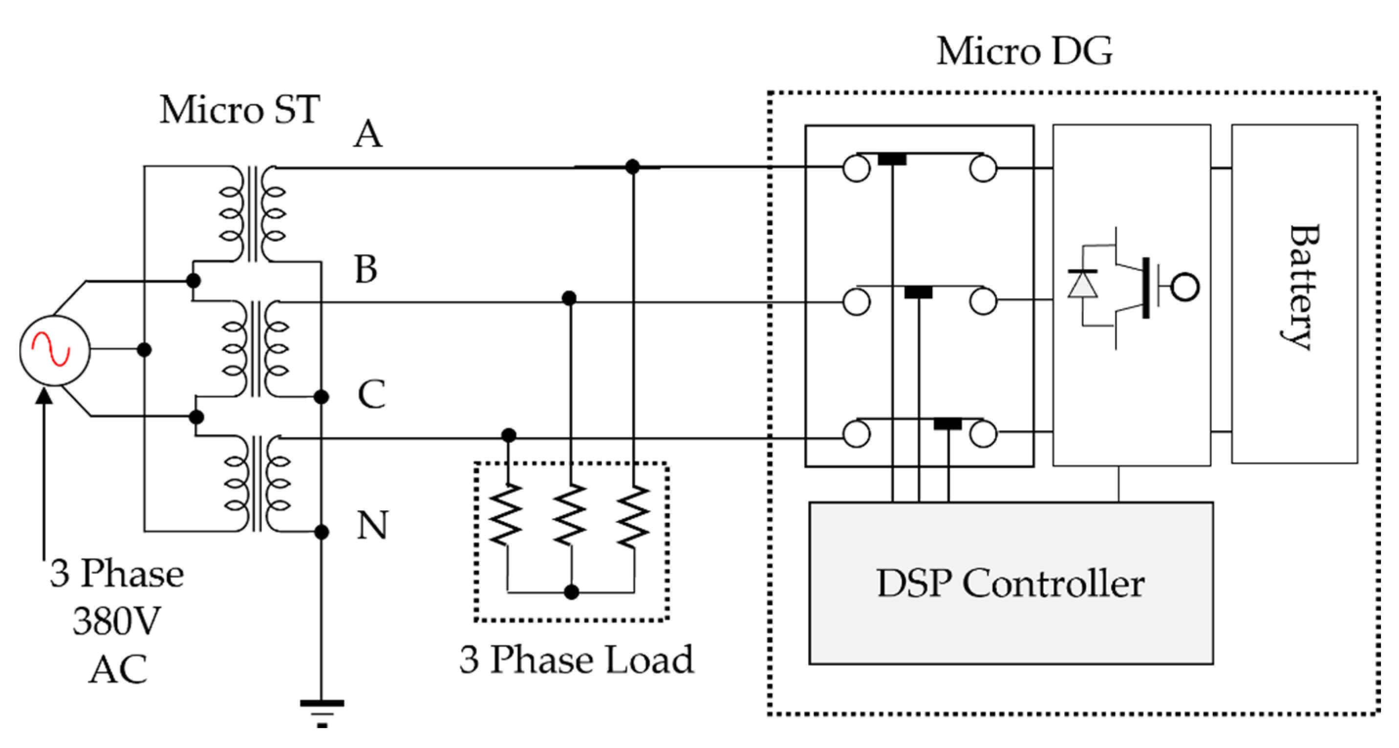
In this paper, the SG is defined as a distribution system with distributed generations that is connected by a digital communication network. In particular, the DG source is represented as a battery source because it is assumed that the DG includes a single battery, and a constant output is possible regardless of variable weather conditions due to the battery. 
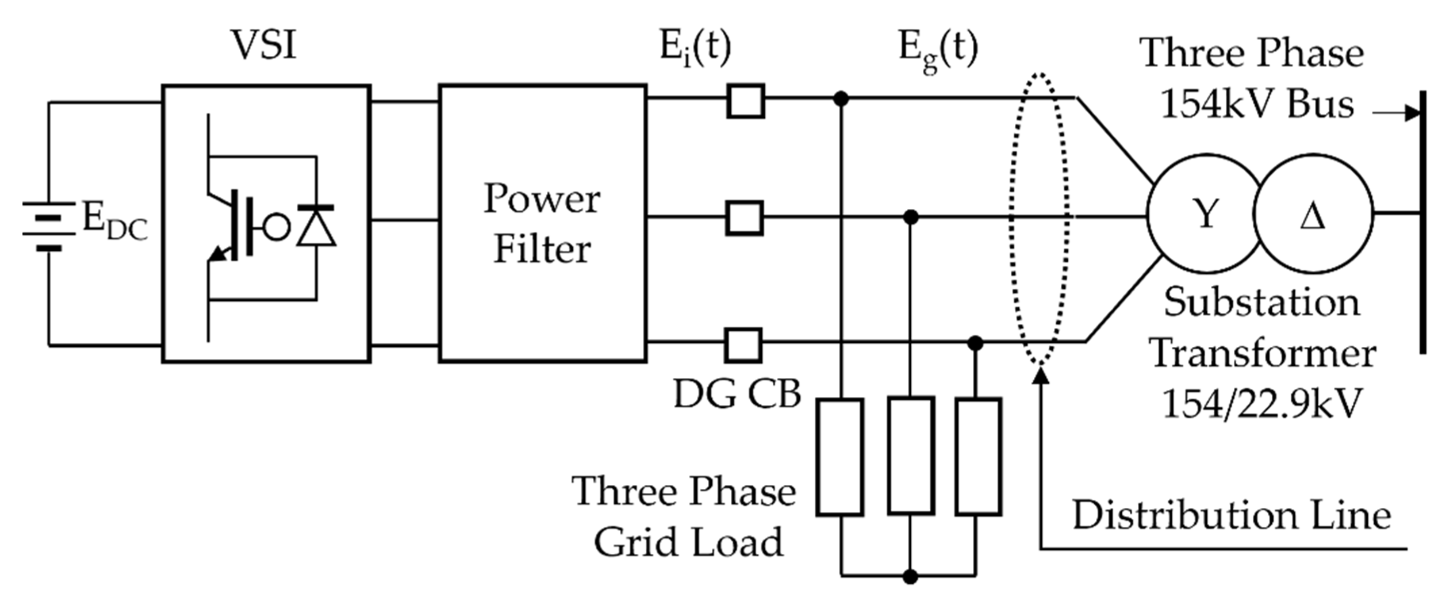
Figure 1 shows the configuration of a representative SG connected with DG.
In Figure 1, EDC is the battery voltage of the DG, VSI is a three-phase voltage source inverter for converting DC power to AC power, and the power filter is a filter to limit the harmonic current flowing from the DG to the SG. In addition, DG CB represents a CB used to connect or separate the DG system from the SG, and “Grid” indicates a three-phase AC power source. The smart-grid-connected operation control of the DG can be divided into two modes. The first mode is a synchronization mode that matches the magnitude and phase of the output voltage of the three-phase inverter to those of the SG voltage. Here, synchronization is required to prevent reactive crossflow, due to voltage magnitude difference, or synchronization current, due to phase difference. After the synchronization is complete, the DG CB is closed to connect the SG with the DG.
The second mode is the PQ control mode used to transmit the required active power and reactive power to the SG at the request of the utility. 
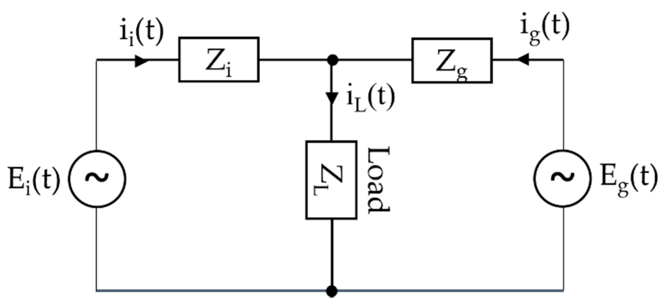
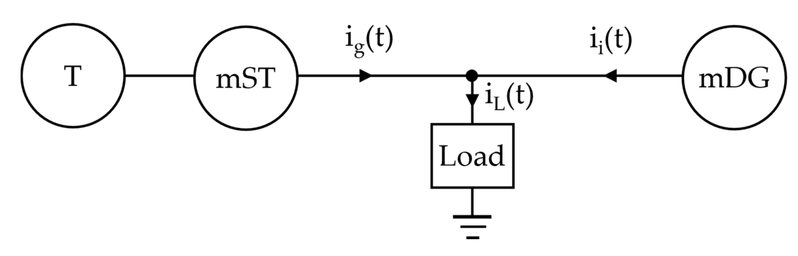
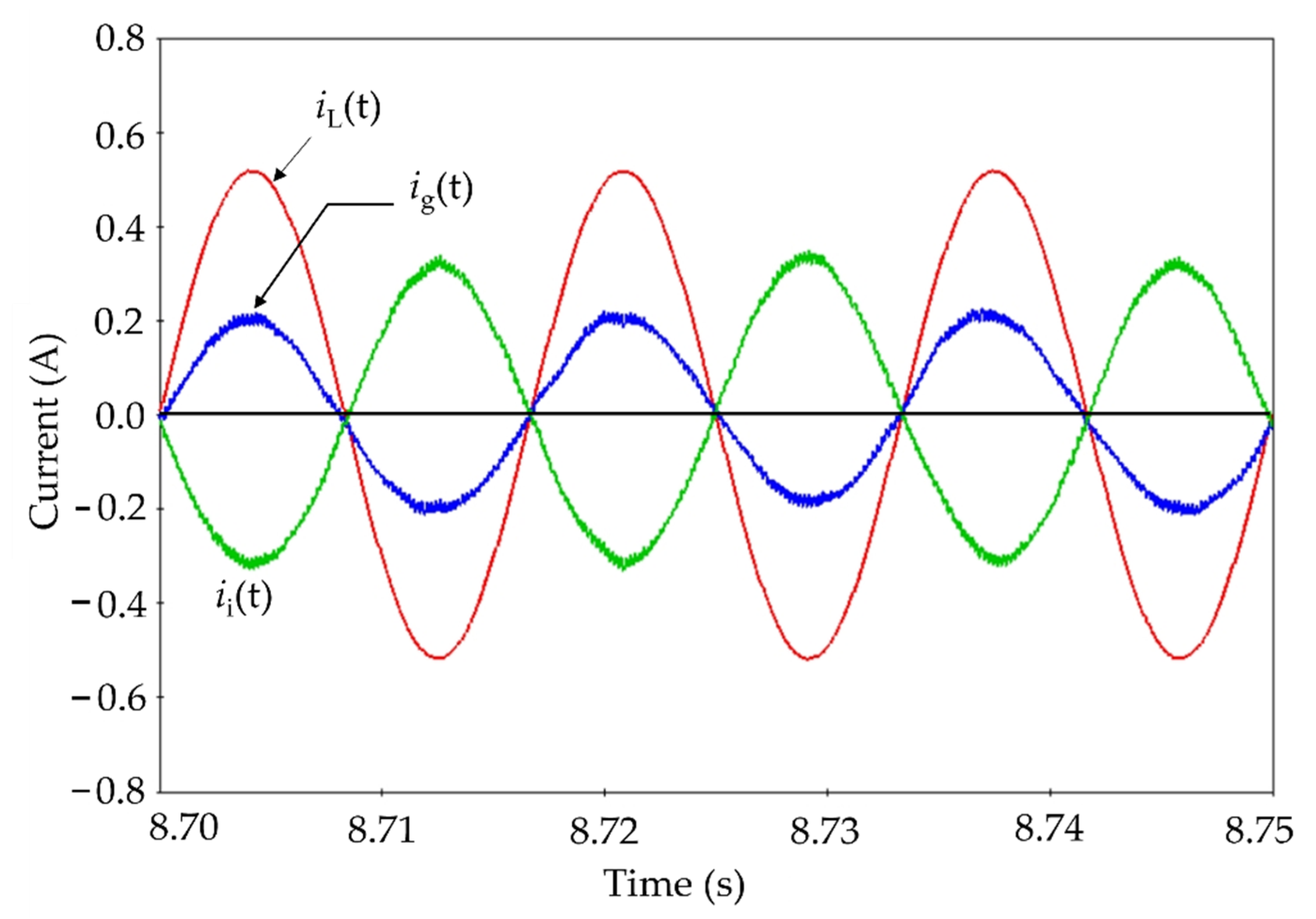
Figure 2 shows the equivalent model of a SG with DG after the DG CB is closed.
The output current of the three-phase PQ-controlled inverter is injected into the grid load through the distribution line of the SG. Simultaneously, the grid current is injected into the grid load through the distribution line from the bank transformer of the SG. After the DG CB is closed (as shown in Figure 2), Ei(t) becomes equal to Eg(t), thus, the load current iL(t) can be expressed using Equation (1).
i L ( t ) = i i ( t ) + i g ( t ) = E g ( t ) / Z L
Here, ii(t) is the inverter output current, ig(t) is the SG line current, Zi is inverter’ output impedance, Zg is SG line impedance, and ZL is the load impedance. Accordingly, for the micro DG on the micro SG simulator to play the same role as that of the DG of the SG, it must have a synchronization function for system connection as well as a PQ control function. In particular, Equation (1) must be satisfied for PQ control under the interconnection operation

3. Design of a Micro DG

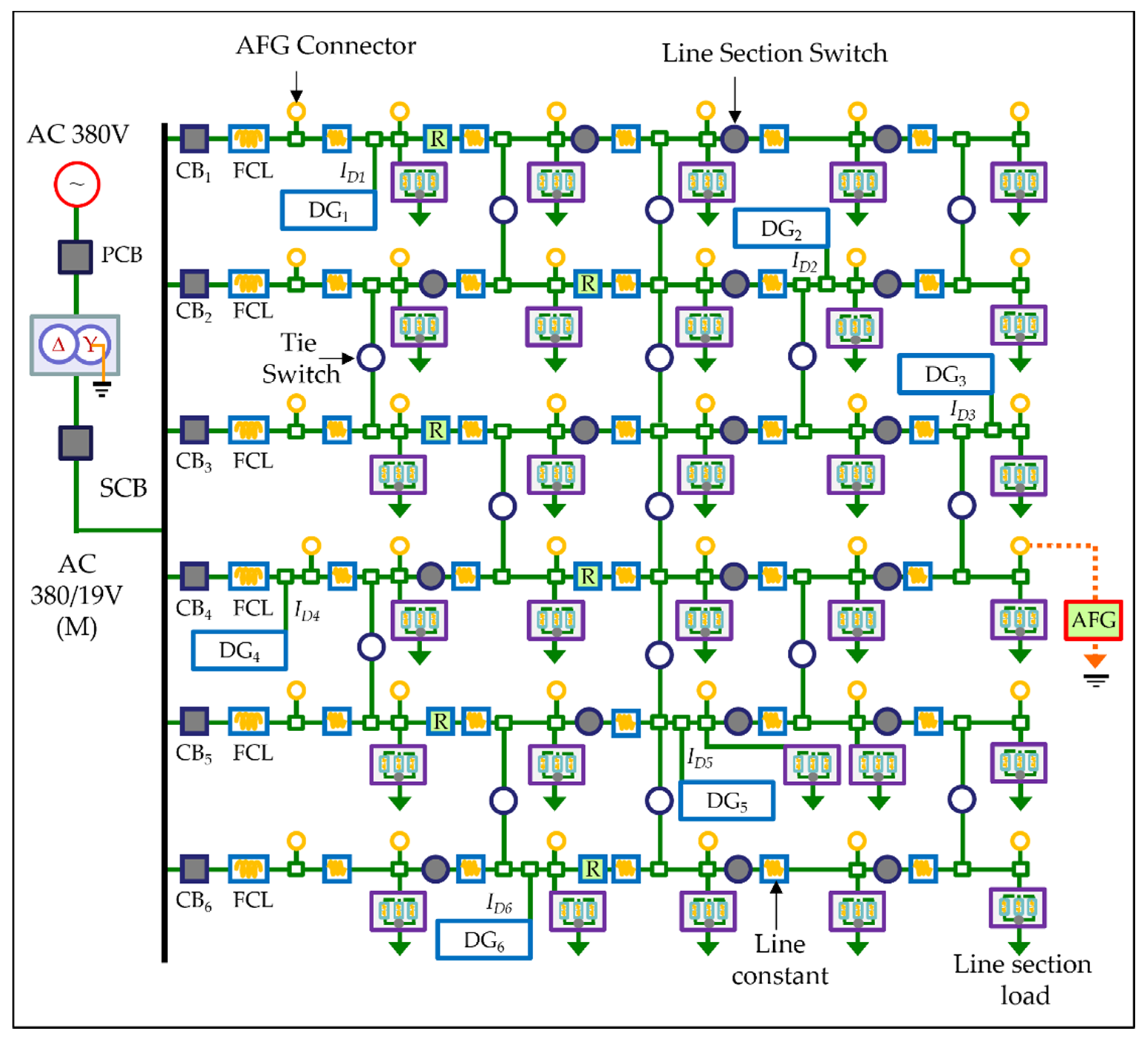
Figure 3 shows the configuration of a micro SG simulator designed with a size of 2 m × 2 m, reduced to 1/1000 of that of the SG via downscaling [20]. A micro substation transformer (micro ST) is a power transformer designed for a micro SG simulator, which has three-phase Δ-Y wiring, a capacity of 190 VA, an output voltage of 19 V, and six distribution lines (micro DLs) as its basic specifications. Here, 19 V is a voltage determined to minimize the size of the protective devices based on the micro SG simulator design procedure.
In Figure 3, Di means the ith micro DG, and the number and location of the micro DGs can be freely added or changed according to the test characteristics, independent of the configuration shown in Figure 3. In this figure, FCL and R represent the fault current limiter and recloser, respectively, and symbols Energies 15 01511 i001 and Energies 15 01511 i002 represent the section and tie switches, respectively; the micro PDs act as CBs, reclosers, section switches or tie switches; AFG is a device that artificially generates any fault at any location on the micro SG simulator.
The micro DG can be realized by reducing the size of the DG and by lowering the electrical level of the DG to meet the design specifications of the micro SG simulator shown in Figure 3. Accordingly, the micro DG is designed with a rated voltage of 19 V and a rated frequency of 60 Hz. Currently, the electric power companies are demanding that the capacity of the DG be increased to a maximum of 30% of the distribution line capacity in the near future. According to this trend, the output capacity of the micro DG is determined to be 7.5 VA, which is 30% of that of the micro DL capacity.
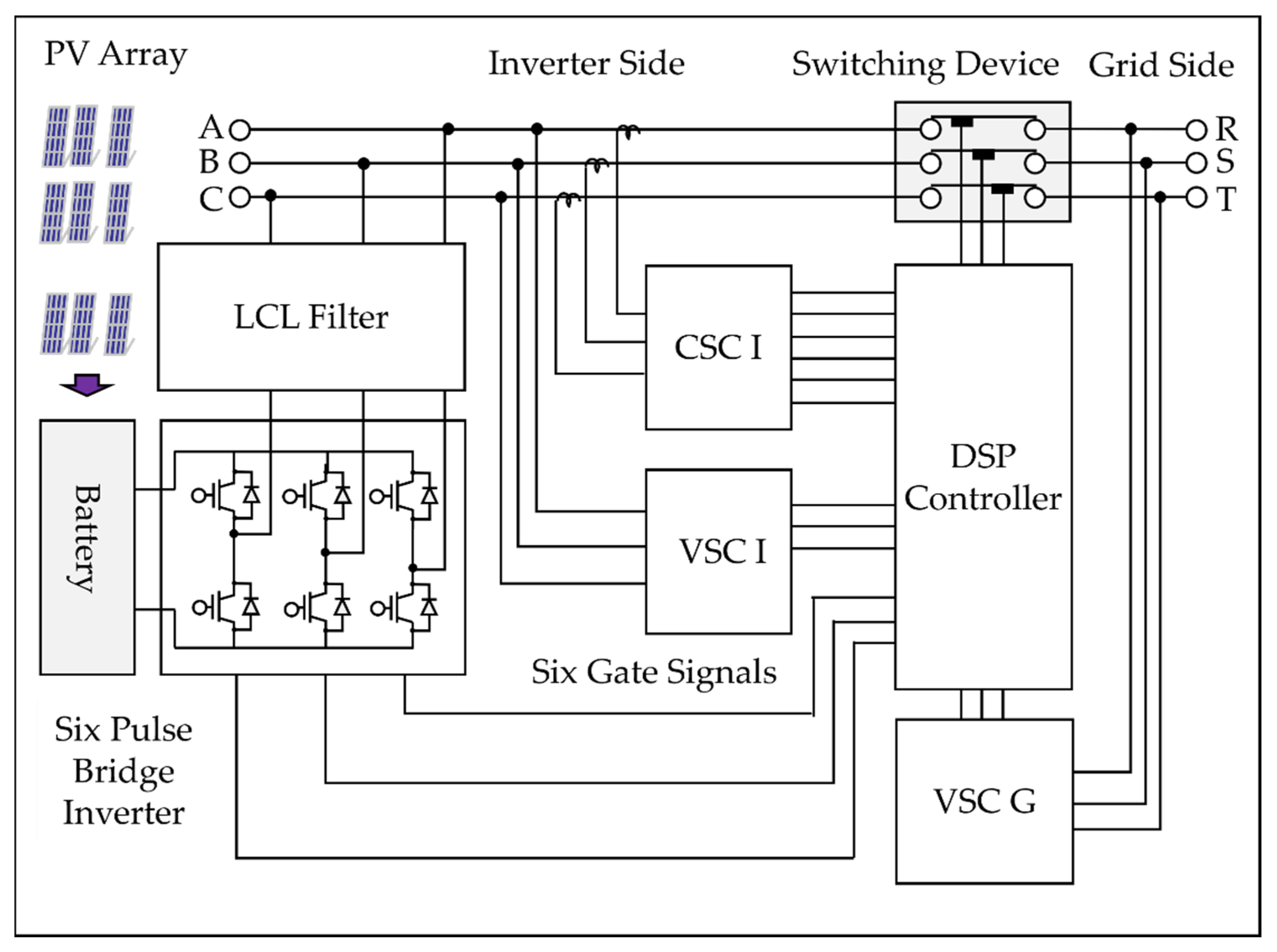
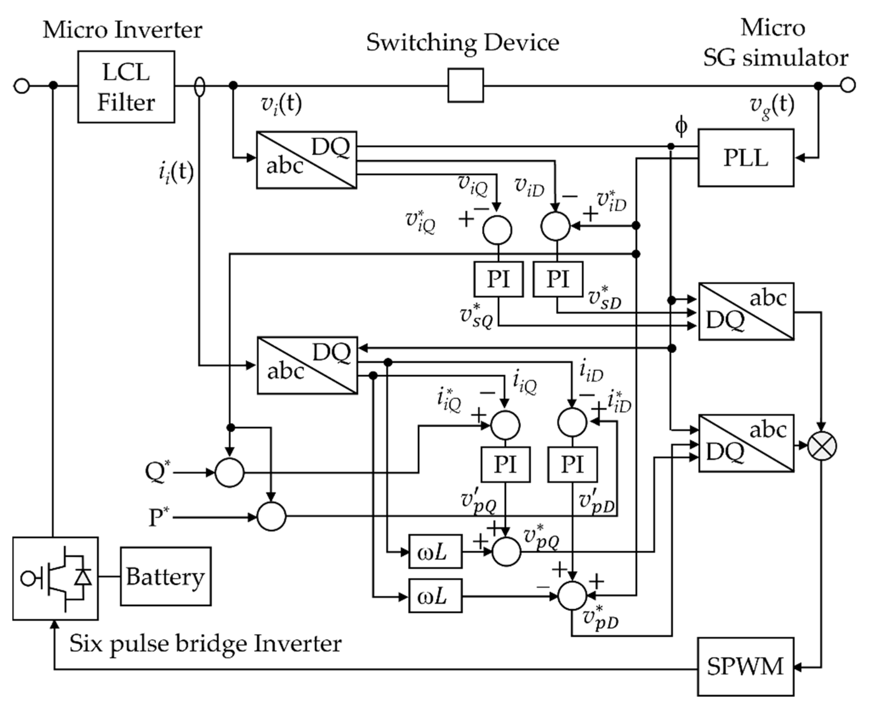
Figure 4 shows the configuration of the proposed micro DG, which consists of a micro inverter, an LCL filter, a power switching device, and a battery.

3.1. Design of the Micro Inverter

Generally, DG includes one inverter as a key element to convert DC power into AC power and supply it to the SG. The micro inverter in the micro SG simulator must play the basic roles of the DG inverter used in the SG. These basic roles include grid synchronization, protection and coordination, and PQ control based on connection operation with the micro SG simulator. To perform these basic roles through connection operation with the micro SG simulator, the micro inverter is designed as a three-phase six-pulse voltage source inverter with a 19 V output voltage, 60 Hz output frequency, and 7.5 W output capacity to satisfy the design specifications of the micro DG as mentioned before.
A voltage sensing circuit VSC I is designed to measure the three-phase voltages of the micro inverter, and a voltage sensing circuit VSC G is designed to measure the three-phase voltages of the micro SG simulator. Their maximum measurable voltage is determined in the range of 1.5 to 2 pu for the nominal phase voltage of the micro SG simulator. Considering the variations in the supply voltage and unexpected overvoltage, 2 pu is adopted as the upper limit of the voltage range. Given that the line-to-line voltage of the micro SG simulator is 19 V, the measurement range for the phase voltage sensing circuits is designed to be 22 Vrms. Furthermore, a current sensing circuit CSC I is designed to measure the three-phase currents of the micro inverter. Its measuring range is designed to be 30 Arms by considering the maximum fault current of the micro SG simulator. In addition, a DSP-based controller is designed to perform the SPWM control of the six-pulse voltage source inverter and to execute the open/close control of the power switching device. This is required to operate and control the grid connection operation based on the voltage and current information provided from these voltage and current measurement circuits.

3.2. Design of the Micro Power Switching Device

The power switching device is designed to connect the micro DG to the micro SG simulator or to prevent the micro DG from any faults on the micro SG simulator. The minimum operating current of the power switching device, IDmoc, can be determined by Equation (2).
I Dmoc = ( 1 + α ) P i 3 V i
Here, α is the safety factor of the operating current to protect the micro DG from external faults. In general, α = 1 is determined in the case of an inrush current suppression circuit, but α = 2 is obtained when no inrush current circuit is considered. As Vi = 19 Vrms and Pi = 7.5 W, the minimum operating current of the power switching device is designed to be 700 mArms, and its breaking capacity is determined to be 5 Arms because the fault current is suppressed by the LCL filter.

3.3. Design of the Battery

The battery is designed to be 13 × 10 cm2 to meet the design specifications of the micro DG. The DC-link voltage of the battery must be designed so that the output voltage of the micro inverter can sufficiently follow the voltage of the micro SG simulator. The micro inverter, LCL filter, and micro SG simulator are connected in a cascading structure. If the output voltage of the inverter follows the grid voltage of the micro SG simulator in the SPWM inverter, then the battery voltage EDC can be determined by Equation (3) as:
E DC = 3 2 E g 2 M   ( 1 + β )  
In Equation (3), M = 0.75, which is the maximum allowable magnitude control ratio of the output voltage to the input voltage in the PWM inverter [25]; β represents the safety factor, and it is determined as the sufficient voltage in consideration of the voltage changes in the supply power or the voltage drop of the inductor. Here, based on experimental experience, it is determined as 1. Accordingly, from Equation (3), the battery voltage EDC is determined to be approximately 62 V.

3.4. Design of the LCL Filter

The LCL filter is designed to remove the harmonic currents flowing from the inverter to the micro SG simulator. Compared to the LC filter, the LCL filter has the advantage of a reduced size and low switching frequency. Initially, the LCL filter is designed according to the LCL filter design procedure proposed in [25,26,27].
Here, the allowable ripple rate, γ, of the inverter-side inductor, the grid’s maximum power factor variation μ, and the harmonic attenuation rate, δ, of the output current to the input injection current of the grid-side inductor are determined to be 20 [%], 5 [%], and 20 [%], respectively. Subsequently, the LCL parameters are modified appropriately through repeated experiments. Table 1 shows the design specifications of the micro DG, determined based on the micro DG design procedure described above. In Table 1, Vi is line-to-line voltage of the micro inverter.

4. Grid Synchronization and PQ Control Algorithms Based on DQ Transform

The proposed grid connection and operational control algorithm, to ensure that the micro DG can play the same role as that of the DG of the SG, is based on the DQ transform method [28]. Figure 5 shows the space vector diagram for grid connection and active power control.
In Figure 5, v g (t), v i (t), and i i (t) are the voltage vector of the grid, output voltage vector of the inverter, and output current vector of the inverter, converted from the three-phase stationary reference frames to the dq stationary reference frame, respectively.
The vector v g (t) becomes the reference vector of the DQ rotating reference frame to determine the control amount of the vectors v i (t) and i i (t) for grid connection and active power control. In grid connection, synchronization is achieved via the following conditions: γ = 0 and making the magnitude of v i (t) equal to that of v g (t).
In contrast, in active power control, the output current vector i i (t) of the inverter is controlled, such that the target active power flows from the inverter to the grid.

4.1. Grid Synchronization Algorithm

The magnitude v iD * (t) and angle φ of v g (t) of the micro SG simulator are obtained from the PLL circuit [29]. Next, the D-axis component, viD, and the Q-axis component, viQ, of v i (t) e j , represented as the DQ rotating reference frame, can be represented as shown in Equation (4).
In Equation (4), TS is a transformation matrix that converts the three-phase output voltages via(t), vib(t), and vic(t) of the inverter to the dq stationary reference frame, and TR is a transformation matrix that converts the d-axis component vid and q-axis component viq represented on the dq stationary reference frame to the DQ rotating reference frame.
[ v iD   v iQ ] = 2 3 T R T S [ v ia   v ib   v ic ]
where, T S = [ 1 1 2 1 2 0 3 2   3 2 ] ,   T R = [ cos   φ sin φ sin   φ cos   φ ]
The reference signal for SPWM, v s * , is determined by converting the signals v sD * and v sQ * , obtained by compensating ε sD and ε sQ using PI controllers, to the three-phase stationary frame using Equation (5):
v s * = [ v sa *   v sb *   v sc * ] = T S T R   [ v sD *   v sQ * ]
Here, ε sD is difference between the magnitudes of the grid voltage v iD * and micro inverter voltage v iD (t), and ε sQ is the phase difference between the grid v iQ * and the micro inverter v iQ . As a result of the output voltage control of the micro inverter, both ε sD and ε sQ must become zero

4.2. PQ Control Algorithm

The output power of the micro inverter can be represented as a space vector using Equation (6).
S = p * + j q * = 2 3 v i ( t ) i i ( t )  
The D- and Q-axis components iiD and iiQ of i i ( t ) e j expressed in the DQ rotating reference frame are obtained by converting the three-phase output currents iia(t), iib(t), and iic(t) of the inverter to the dq stationary reference frame and then to the DQ rotating reference frame as shown in Equation (7).
[ i iD   i iQ ] = 2 3 T R T S [ i ia   i ib   i ic ]
Simultaneously, the target current values, i iD * and i iQ * , are calculated by dividing the target active power value, p*, and the target reactive power value, q*, by the grid voltage v iD * , respectively (Equation (6)). Next, v pD and v pQ are obtained by compensating ε pD and ε pQ using PI controllers. Here, ε pD corresponds to the difference between the magnitude of the target active current, i iD * and that of the actual active current, i iD , whereas ε pQ corresponds to the difference between the magnitude of the target reactive current, i iQ * , and that of the actual reactive current, i iQ . Subsequently, by compensating the coupling effect of the LCL filter, v pD * and v pQ * are obtained.
Finally, the reference signal v p * of the SPWM, for the output power control of the micro inverter is obtained by converting the signals v pD * and v pQ * to the three-phase stationary reference frame using Equation (8) as:
v p * = [ v pa *   v pb *   v pc * ] = T S T R [ v pD *   v pQ * ]
For the output power control of the micro inverter, both ε pD and ε pQ must become zero. Accordingly, the procedure of Equation (7) to (8) is repeated until both ε pD and ε pQ are obtained within an acceptable tolerance. Figure 6 shows grid synchronization and the PQ control algorithm of micro DG.

5. EMTP Modelling and Simulation

5.1. Modelling of a Micro DG

To verify the effectiveness of the developed synchronization and PQ control algorithms and to assess their validity for a micro SG simulator scaled down to a three-phase 19 V system, one micro DG is developed in the form of an EMTP model using EMTP-RV [30] using the parameters specified in Table 1. This modelled micro DG contains a micro three-phase voltage source inverter, an LCL filter, a PI voltage controller for grid synchronization, a PI current controller for PQ output control, an SPWM, and a battery. This is developed to examine the electrical dynamics such as the magnitude and direction of the current during the connection operation. The developed EMTP-RV model of the micro DG is represented as mDG in Figure 7.

5.2. Simulation Evaluation

To identify the effectiveness of the DQ transform- and SPWM-based grid synchronization as well as of the PQ control algorithm and to analyze the dynamic electrical characteristics such as the direction and magnitude of the current during the connection operation between the DG and the SG, the developed EMTP model is evaluated under one test line using EMTP-RV.
Figure 7 shows the test line, where T is a 22,900/380 V distribution transformer. The test contains an mST, a micro substation transformer, three-phase Δ-Y connection, a line voltage of 19 V, and a three-phase capacity of 190 VA. The mDG is an EMTP model of the micro DG, and L represents a three-phase load consisting of three 30 Ω resistors.
Figure 8 shows the EMTP-RV simulation results of the phase output voltage via(t) of the inverter, following a phase voltage vga(t) of the micro SG simulator, obtained using the synchronization algorithm. The validity of the proposed synchronization algorithm is confirmed by the magnitude and phase of via(t) of the inverter, exactly matching those of vga(t) of the micro SG simulator.
Figure 9 and Figure 10 show the EMTP-RV simulation results for the PQ output control algorithm. Figure 9 presents the micro inverter output current for a PQ control simulation case. Evidently, the magnitude of the three-phase output current of the micro inverter can be accurately controlled to 228 mA, according to the PQ control command.
From Figure 10, it is confirmed that the accurate active power, p(t), and reactive power, q(t), of the micro inverter are 7.5 W and 0 VAR, respectively. These values are obtained by controlling the output current of the micro inverter, as shown in Figure 9, using the PQ control command.
Through the results shown in Figure 9 and Figure 10, the effectiveness of the DQ transformation and SPWM-based power control algorithm can be verified. The dynamic electrical characteristics of the general SG in connection operation with the DG are as follows. When the DG operates independently, the entire load current on the SG is supplied by the power source of the SG. In contrast, when the DG is connected and operated in the constant output power mode, the power source provides a load current other than the current supplied by the DG.
In Figure 11, the power source of the micro SG simulator supplies the entire load current of 366 mArms before connecting the micro DG. Conversely, if the micro DG is connected and the constant output power is operated at 7.5 W, then approximately 228 mArms flows from the micro DG, and thus, the micro ST supplies the remaining load current. Figure 11 confirms that Equation (1) is satisfied.
From the simulation results, it can be seen that when the micro SG simulator and micro DG are connected and operated, the dynamic electrical characteristics such as the magnitude and direction of the current are the same as those observed in an SG operating in the connected mode

6. Experimental Results

Based on the specifications listed in Table 1, and the EMTP modeling results discussed in the previous section, a micro DG is experimentally designed and implemented, and an experimental line of a micro SG simulator is built. Next, the synchronization and PQ control experiments are performed by connecting the micro three-phase inverter with the experimental line of the micro SG simulator. Through this experiment, the effectiveness of the implemented algorithm is experimentally verified, and it is confirmed that the electrical characteristics obtained in the connection operation between the micro inverter and the micro SG simulator are almost the same as those obtained in the connection operation between the actual DG and the SG.

6.1. Experimental System Configuration

The experimental set up for performing the connection and operation control experiments between a micro inverter and a micro SG simulator is shown in Figure 12.
As shown in Figure 13, a three-phase transformer with a capacity of 190 VA is used as the power source, the line-to-line voltage is 19 V, and a Δ-Y wiring connection with the specifications of the micro SG simulator is implemented in the experimental set up. Furthermore, three Y-connected 30 Ω resistors form the three-phase load. A normal open-type relay HR 702NH is used as the power switching device for the grid connection/disconnection and fault current breaking, and DSP TMS 320F28335 is used as the main controller of micro inverter.

6.2. Grid Synchronization Verification

Figure 14 shows the three-phase output voltage waveforms of the micro inverter after the synchronization. Figure 15 shows the phase voltage waveforms of the micro SG simulator (channel C2) and micro inverter (channel C3) after the synchronization. From Figure 15, it is confirmed that the micro SG simulator voltage is 11.3 Vrms, and the magnitude and phase of the output voltage of the inverter are exactly the same as those of the micro SG simulator voltage. Thus, these experimental results demonstrate the effectiveness and validity of the proposed synchronization algorithm.

6.3. PQ Control Verification

In the PQ control experiment, the currents are measured in units of V using the current sensor modules. Notably, the ratio of the current value, in units of V, to the actual current value, in units of A, is approximately 1:1.
Figure 16 shows three-phase output current waveforms of the micro inverter for the 7.5 W–0 VAR PQ control command. Figure 17 presents the result of a three-phase 7.5 W PQ control experiment, showing the phase output current (channel C4) of the micro inverter flowing to the load, phase line current (channel C2) flowing from the micro ST to the load, and phase load current (channel C3), respectively under PQ control. The output current (channel C4) of the micro inverter flows in the reverse direction compared to that of the other currents (channel C2 and C3). From Figure 17, it can be identified that the load current (channel C3) is almost equal to the sum of the micro ST line current and micro inverter output current (channel C2 + channel C4), implying that the condition represented by Equation (1) is satisfied. This indicates that when the micro DG and micro SG simulator are connected together, the changes in the voltage and current magnitudes or current direction are the same as those obtained in a DG–SG connected system.
The prototype of the micro DG was manufactured based on the experimental results. The micro inverter of micro DG, to satisfy the design specifications of the micro DG, was designed with several boards, each of size 13 × 13 cm2, and each board performs its basic roles. Boards designed for the micro inverter include a micro inverter DSP controller board, a micro inverter voltage measuring board, a micro SG simulator, a voltage measuring board, a micro inverter current measuring board, a micro inverter switching device board, a micro 6-pulse bridge inverter and filter board, and a power supply board. Figure 18 shows prototype of the micro DG manufactured based on the experimental results.

7. Conclusions

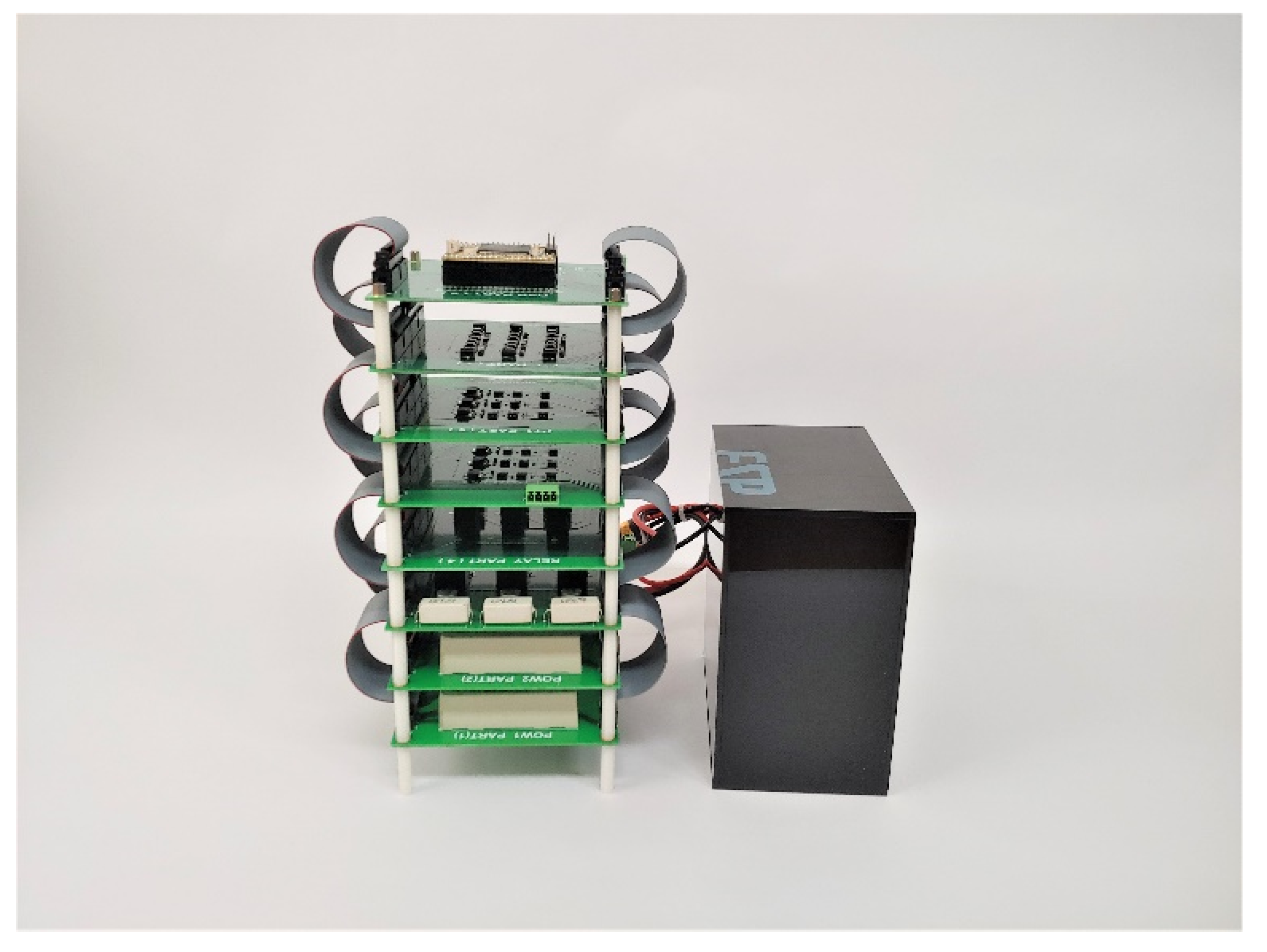
In this paper, a method is proposed for the miniaturization of DG, required to develop a micro DG. Using this proposed method, a micro DG was designed and developed as a three-phase structure with an output voltage of 19 V and a rated capacity of 7.5 W in accordance with the design specifications of a micro SG simulator. In particular, the micro DG was developed with a size of 13 × 20 cm2 by designing each function of the micro inverter on a 13 × 13 cm2 circuit board with a multi-layered structure. A DQ frame-based synchronization was performed, and a PQ control algorithm was developed for operating the micro DG and micro SG simulator in connected mode.
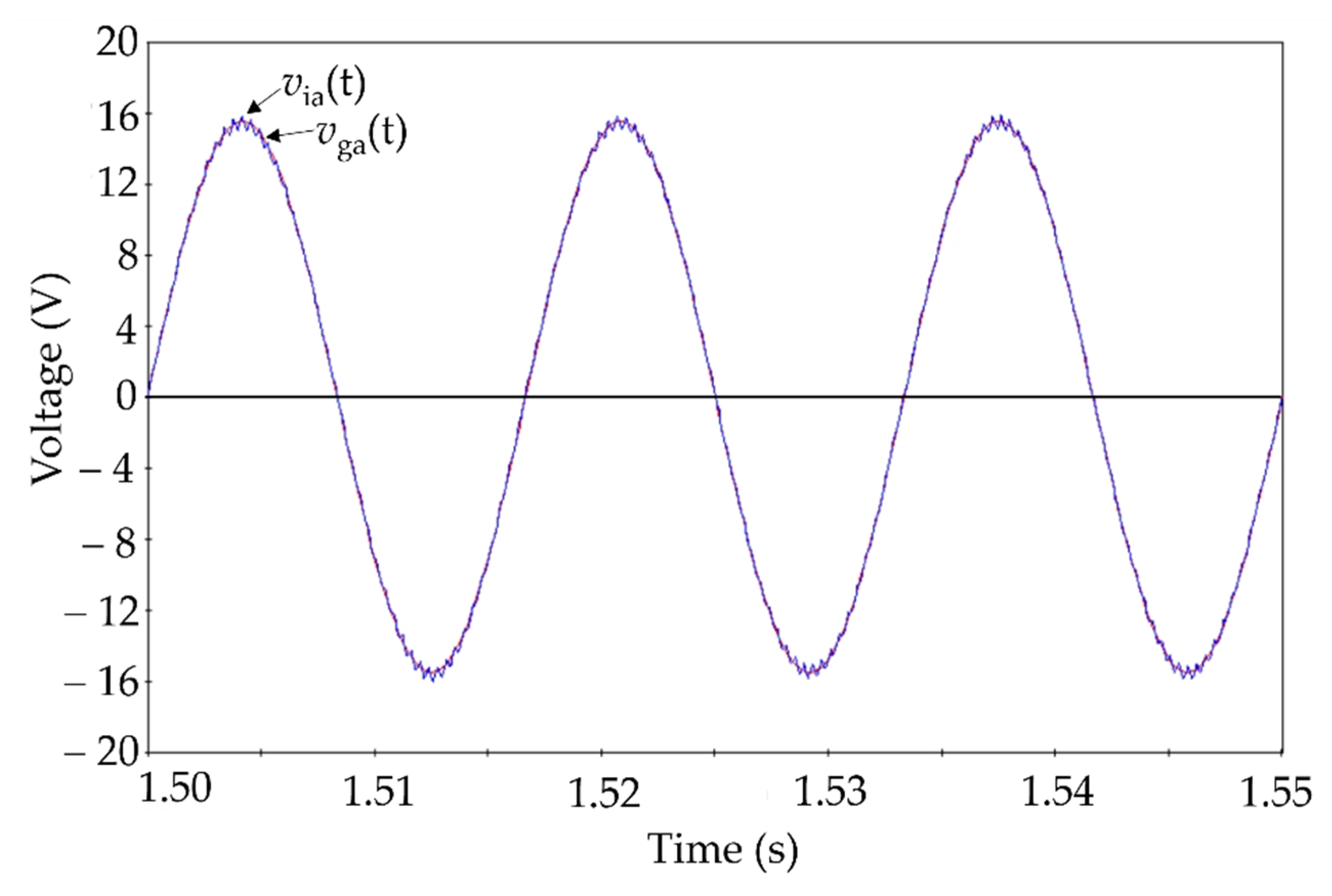
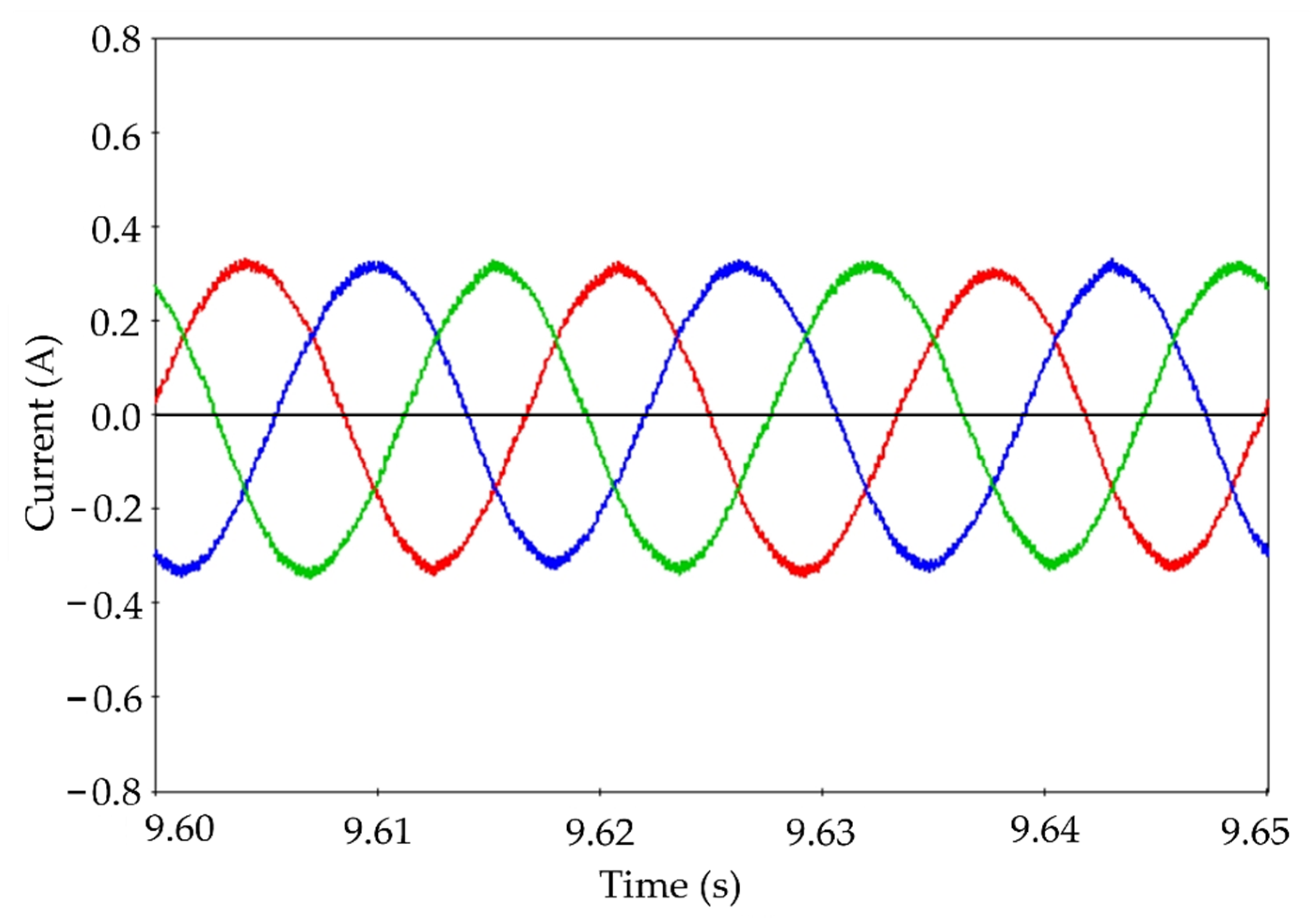
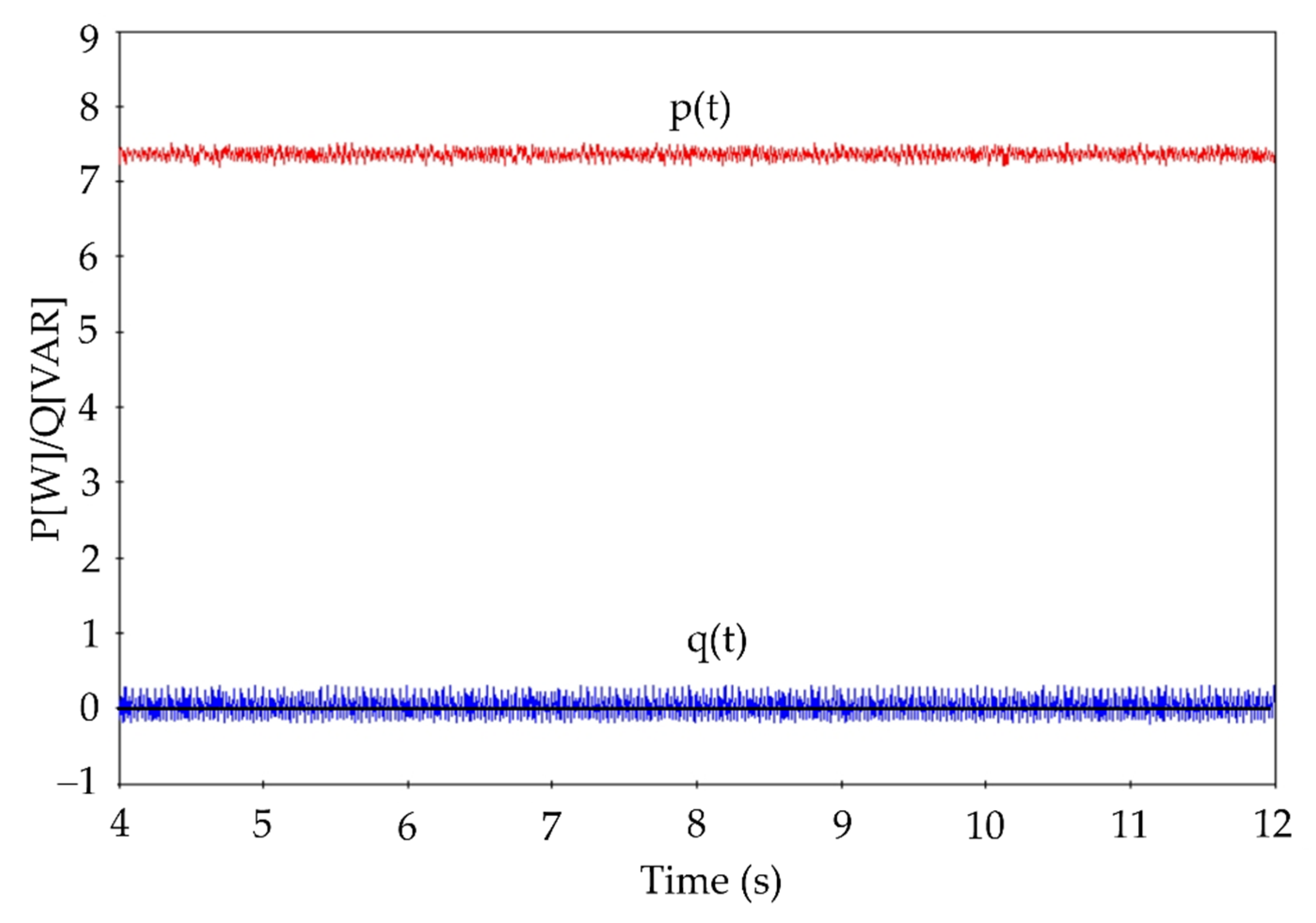
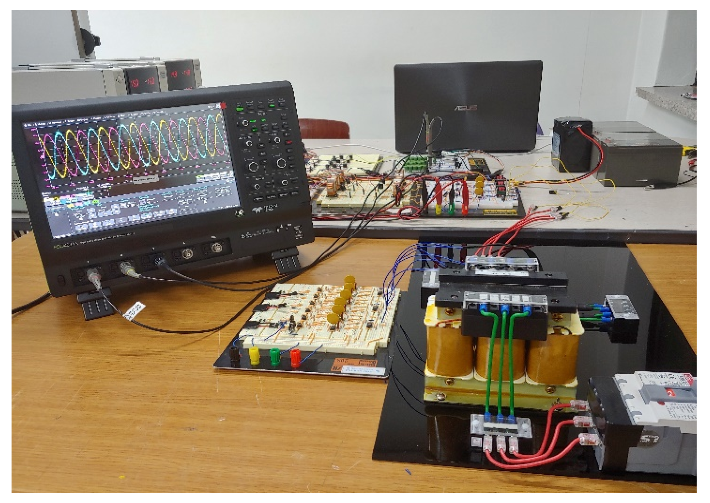
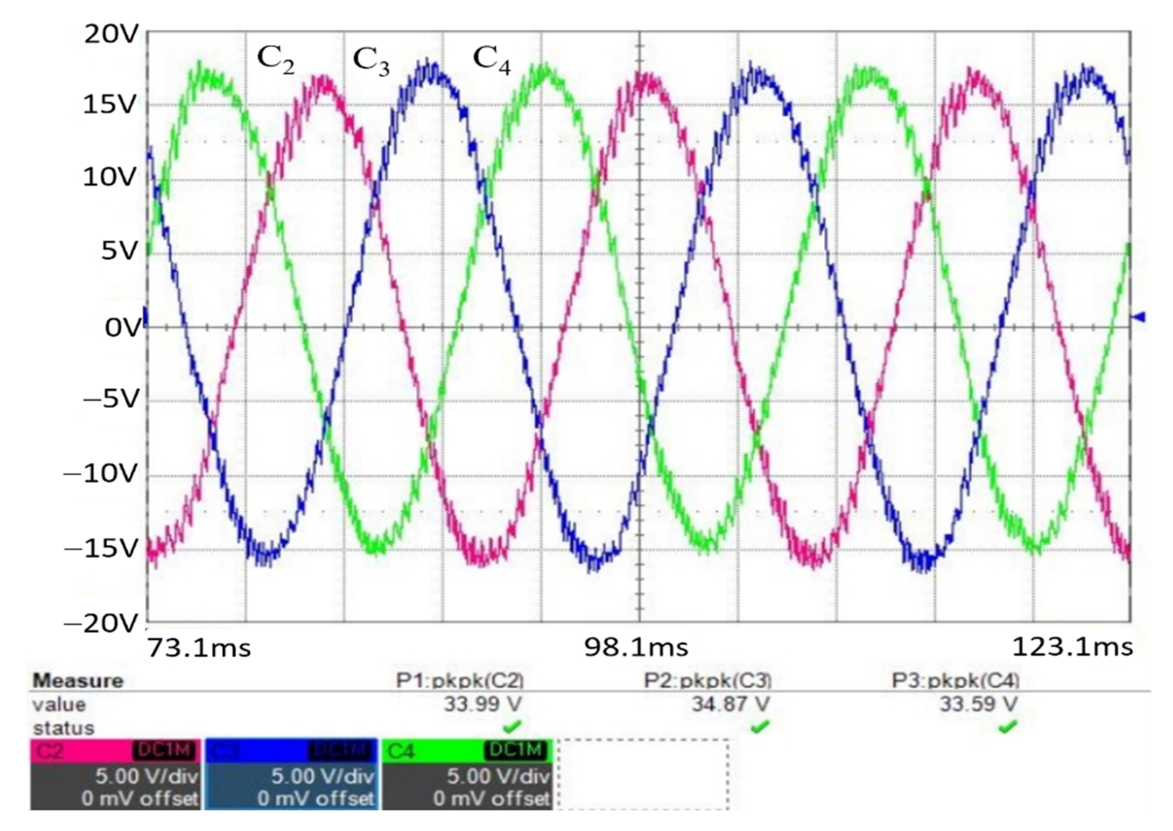
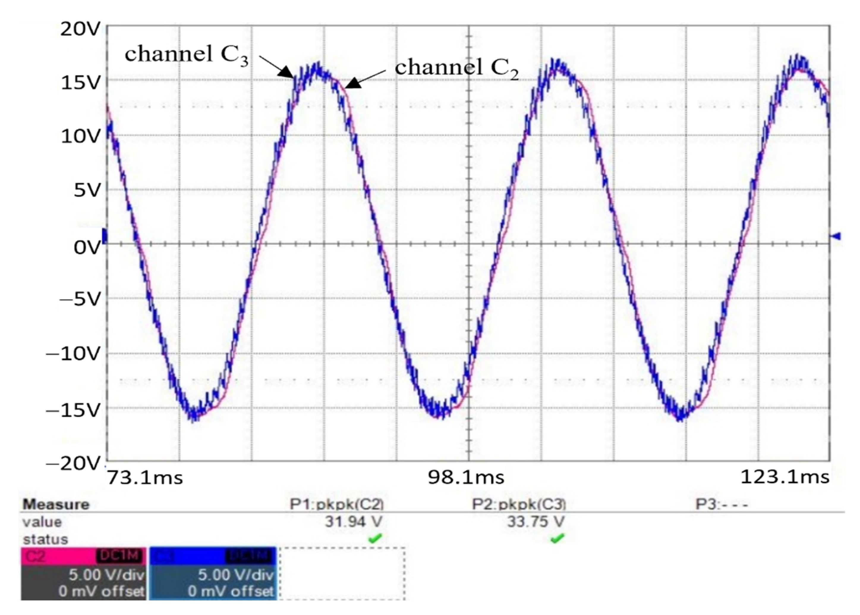
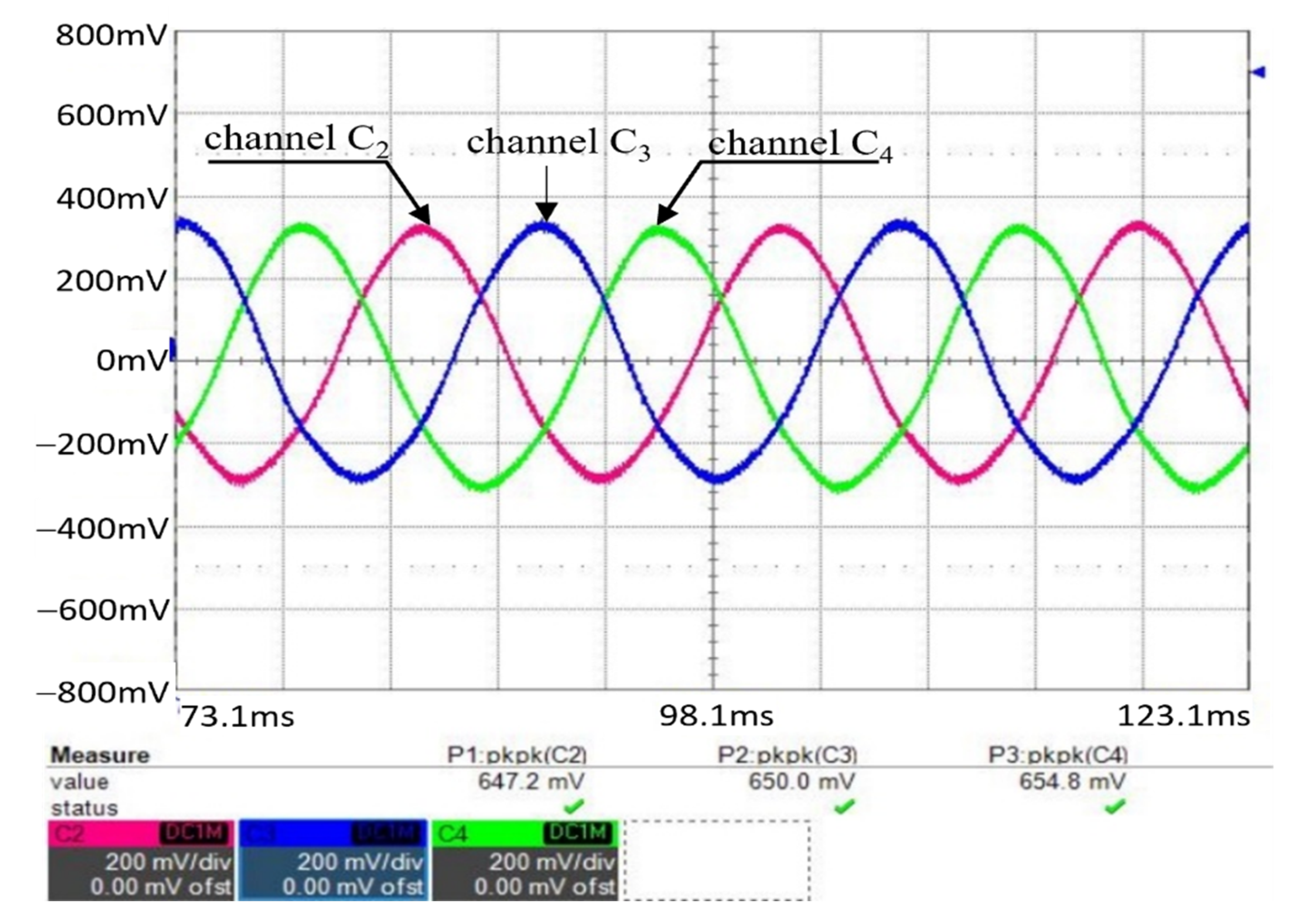
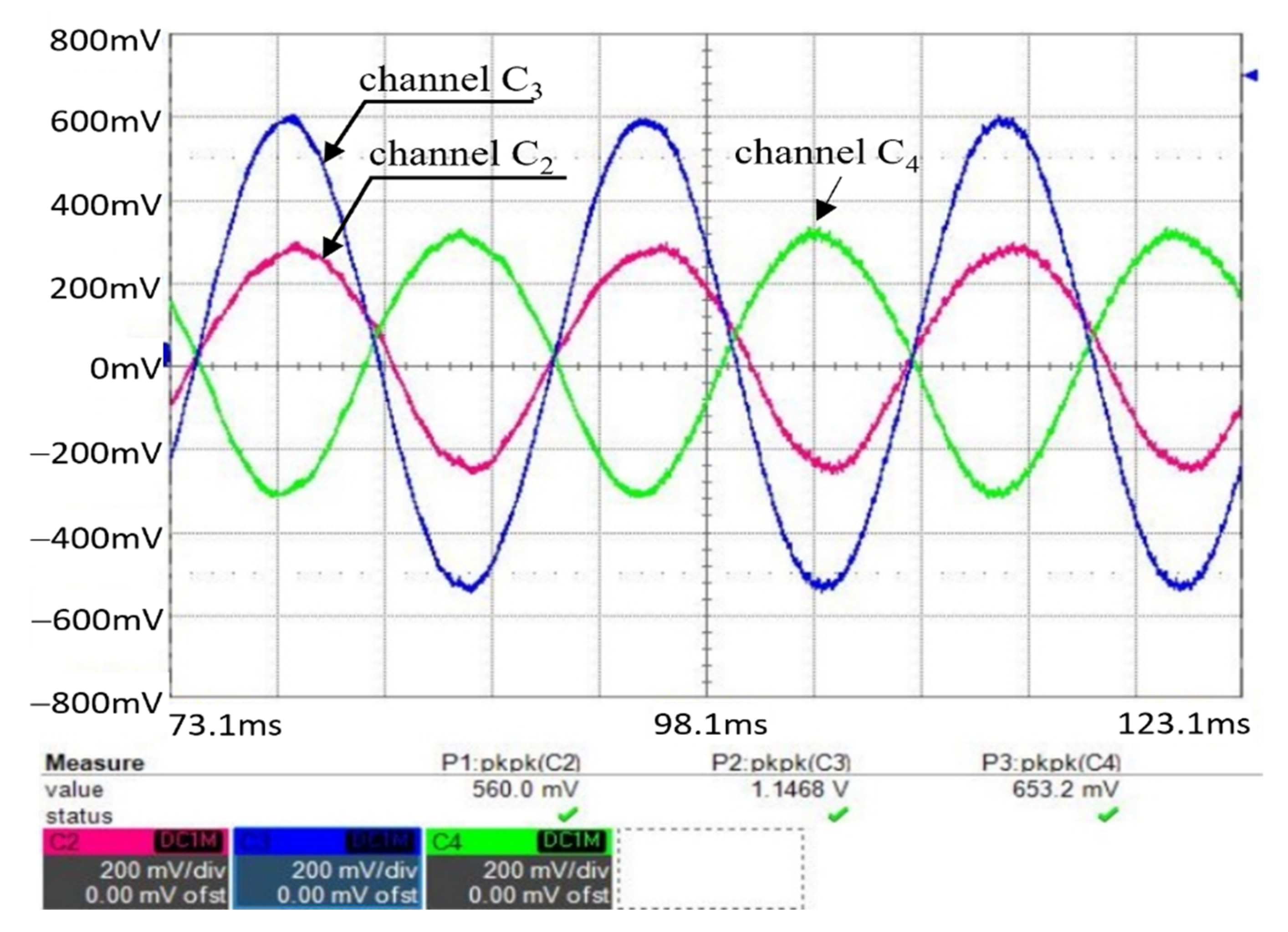
Initially, a micro DG was modeled as an EMTP model, and the validity of the developed algorithm was verified through EMTP-RV simulation. It was confirmed that the magnitude and phase of the output voltage of the micro inverter were the same as those of the test-system voltage. Further, it was identified that the output of the micro inverter model accurately followed the PQ control command of 7.5 W. These results verify the effectiveness of the developed algorithm. Based on this algorithm, a prototype of the DG was prepared, and a test system, based on a test line corresponding to the micro SG simulator, was constructed. Using the test system, it was confirmed that the magnitude and phase of the output voltage of the micro inverter matched exactly those of the test-system voltage. Moreover, the active and reactive powers of the micro inverter could be controlled within 10% of the maximum allowable error range using the PQ control command. Furthermore, the dynamic electrical characteristics of the DG–SG connected system were found to be approximately the same as those observed when a micro DG was connected and operated with the micro SG simulator.
In conclusion, it was established that the proposed method for the miniaturization of DG was highly effective, and the subsequently developed micro DG could be successfully applied in a micro SG simulator. Thus, it is expected that the micro DG, prepared using the proposed method, can serve as a DG for developing new operation control algorithms for SGs.

Author Contributions

Methodology, Y.-S.K.; investigation, Y.-S.K., S.-H.K. and G.-H.L.; writing—original draft preparation, Y.-S.K.; project administration, Y.-S.K. All authors have read and agreed to the published version of the manuscript.

Funding

This work was supported by the National Research Foundation of Korea Grant funded by the Korean Government (NRF-2016R1D1A1B01013749).

Institutional Review Board Statement

Not applicable.

Informed Consent Statement

Not applicable.

Data Availability Statement

Not applicable.

Conflicts of Interest

The authors declare no conflict of interest.

References

  1. Taylor, T.; Lubkeman, D. Implementation of Heuristic Search Strategies for Distribution Feeder Reconfiguration. IEEE Trans. Power Deliv. 1990, 5, 239–246. [Google Scholar] [CrossRef]
  2. Liu, J.; Cheng, H.; Shi, X.; Xu, J. A Tabu Search Algorithm for Fast Restoration of Large Area Breakdown in Distribution Systems. Energy Power Eng. 2010, 2, 1–5. [Google Scholar] [CrossRef] [Green Version]
  3. Ko, Y.-S. A Self-Isolation Method for the HIF Zone under the Network-Based Distribution System. IEEE Trans. Power Deliv. 2009, 24, 884–891. [Google Scholar]
  4. Shin, C.-H.; Yun, G.-G.; Jo, S.-S.; Jeong, W.-O.; Shin, D.-Y.; Park, M.-H.; Jung, J.-S.; Rho, D.-S.; Kim, J.-E.; Jang, G.-S.; et al. A Study on the Actual Examination of Bidirectional Protection for Interconnecting Distributed Resources with Distribution System; Technical Report TR-H02. S2009.0998; Korea Electric Power Research Institute: Daejeon, Korea, 2009. [Google Scholar]
  5. Milioudis, A.N.; Andreou, G.T.; Labridis, D.P. Enhanced Protection Scheme for Smart Grids Using Power Line Communications Techniques—Part II: Location of High Impedance Fault Position. IEEE Trans. Smart Grid. 2012, 3, 1621–1630. [Google Scholar] [CrossRef]
  6. Cheng, Y.; Podlaski, M.; Schmall, J.; Huang, S.-H.F.; Khan, M. ERCOT PSCAD Model Review Plat-form Development and Performance Comparison with PSS/e Model. In Proceedings of the 2020 IEEE Power & Energy Society General Meeting (PESGM), Montreal, QC, Canada, 2–6 August 2020. [Google Scholar]
  7. Chen, G.; Li, M.; Lu, X.; Zeng, W. Research on Lightning Overvoltage in Ecuador 230kV GIS Sub-station based on EMTP-RV. In Proceedings of the 2021 IEEE 4th International Electrical and Energy Conference (CIEEC), Wuhan, China, 28–30 May 2021. [Google Scholar]
  8. da Costa, L.A.; Gazzana, D.D.; Leborgne, R.C. Fault Location on Point-to-Point HVDC Transmission System by the Electromagnetic Time-Reversal-Based Method. In Proceedings of the 2021 IEEE International Conference on Environment and Electrical Engineering and 2021 IEEE Industrial and Commercial Power Systems Europe (EEEIC/I&CPS Europe), Bari, Italy, 7–10 September 2021. [Google Scholar]
  9. Sanchez, A.; de Castro, A.; Garrido, J. Parametrizable Fixed-Point Arithmetic for HIL with Small Simulation Steps. IEEE J. Emerg. Sel. Top. Power Electron. 2019, 7, 2467–2475. [Google Scholar] [CrossRef]
  10. Lee, J.S.; Choi, G. Modeling and Hardware-in-the-Loop System Realization of Electric Machine Drives—A Review. CES Trans. Electr. Mach. Syst. 2021, 5, 194–201. [Google Scholar] [CrossRef]
  11. Frazier, A.B.; Warrington, R.O.; Friedrich, C. Miniaturization Technologies: Past, Present, Future. IEEE Trans. Ind. Electron. 1995, 42, 423–430. [Google Scholar] [CrossRef]
  12. Horowitz, S.; Mathias, D.; Hernandez, C.; Sanghadasa, M.; Ashley, P. Miniaturization of Piezoelectric Microphones; American Institute of Aeronautics and Astronautics: Atlanta, GA, USA, 2012. [Google Scholar]
  13. Gronland, T.A.; Rangsten, P.; Nese, M.; Lang, M. Miniaturization of components and systems for space using MEMS-technology. Acta Astronaut. 2007, 61, 228–233. [Google Scholar] [CrossRef]
  14. Lee, C.; Yeh, J.A. Development and Evolution of MOEMS Technology in Variable Optical Attenuators. J. Micro/Nano Lithogr. MEMS MOMES 2007, 7, 021003. [Google Scholar]
  15. Piljek, P.; Keran, Z.; Math, M. Micromaching—Review of Literature from 1980 to 2010. Interdiscip. Descr. Complex Syst. 2014, 12, 1–27. [Google Scholar] [CrossRef]
  16. Burns, M.A.; Johnson, B.N.; Brahmasandra, S.N.; Handique, K.; Webster, J.R.; Krishnan, M.; Sammarco, T.S.; Man, P.M.; Jones, D.; Heldsinger, D.; et al. An Integrated Nanoliter DNA Analysis Device. Science 1998, 16, 484–487. [Google Scholar] [CrossRef] [PubMed] [Green Version]
  17. Kurniawan, Y.S. Micro Total Analysis System Application for Biomedicals: A Mini-Review. Biomed. J. Sci. Tech. Res. 2019, 12, 9442–9443. [Google Scholar] [CrossRef]
  18. Bardina, J.; Thirumalainambi, R. Micro-Flying Robotics in Space Missions. SAE Int. J. Aerosp. 2005, 114, 1368–1374. [Google Scholar]
  19. Mondada, F.; Franzi, E.; Ienne, P. Mobile Robot Miniaturisation: A Tool for Investigation in Control Algorithms. In Proceedings of the 3rd International Symposium on Experimental Robotics, Kyoto, Japan, 28–30 October 1993. [Google Scholar]
  20. Ko, Y.-S. A Study on the Effective Downscaling Methodology for Design of a Micro Smart Grid Simulator. J. Electr. Eng. Technol. 2018, 13, 1425–1437. [Google Scholar]
  21. Ko, Y.-S.; Ryu, K.; Oh, M.-S.; Yoon, H.-S. A Study on the Miniaturization of Protective Device for Micro Smart Grid Simulator. J. Electr. Eng. Technol. 2020, 15, 85–94. [Google Scholar] [CrossRef]
  22. Hassan, M.A.; Worku, M.Y.; Abido, M.A. Optimal Power Control of Inverter-Based Distributed Generations in Grid-Connected Microgrid. Sustainability 2019, 11, 5828. [Google Scholar] [CrossRef] [Green Version]
  23. Spring, A.; Wirth, G.; Becker, G.; Pardatscher, R.; Witzmann, R. Grid Influences from Reactive Power Flow of Photo-voltaic Inverters with a Power Factor Specification of One. IEEE Trans. Smart Grid 2016, 7, 1222–1229. [Google Scholar] [CrossRef]
  24. Aillane, A.; Chouder, A.; Dahech, K.; Damak, T.; Ferahtia, S.A. P/Q Control of Grid-Connected Inverters. In Proceedings of the 2021 18th International Multi-Conference on Systems, Signals & Devices (SSD), Monastir, Tunisia, 22–25 March 2021. [Google Scholar]
  25. Liserre, M.; Blaabjerg, F.; Hansen, S. Design and Control of an LCL-filter based Three-phase Active Rectifier. IEEE Trans. Ind. Appl. 2005, 41, 1281–1291. [Google Scholar] [CrossRef]
  26. Ahmed, K.H.; Finney, S.J.; Williams, B.W. Passive Filter Design for Three-Phase Inverter Interfacing in Distributed Generation. In Proceedings of the Electrical Power Quality and Utilisation, Gdansk, Poland, 29 May–1 June 2007; Volume 13, pp. 49–58. [Google Scholar]
  27. Reznik, A.; Simões, M.G.; Al-Durra, A.; Muyeen, S.M. LCL Filter Design and Performance Analysis for Grid-Interconnected Systems. IEEE Trans. Ind. Appl. 2014, 50, 1225–1232. [Google Scholar] [CrossRef]
  28. Trzynadlowski, A.M. Introduction to Modern Power Electronics, 2nd ed.; John Wiley and Sons Inc.: Hoboken, NJ, USA, 2010. [Google Scholar]
  29. Silva, S.M.; Lopes, B.M.; Filho, B.J.C.; Campana, R.P.; Bosventura, W.C. Performance Evaluation of PLL Algorithms for Single-phase Grid-connected Systems. In Proceedings of the IAS2004, Seattle, WA, USA, 3–7 October 2004; pp. 2259–2263. [Google Scholar]
  30. EMTP-RV, Version 3.0; User Manual; Powersys: Le Puy-Sainte-Réparade, France, 2010.
Figure 1. Configuration of SG connected with DG.
Energies 15 01511 g001
Figure 2. Equivalent model of SG connected with DG.
Energies 15 01511 g002
Figure 3. Configuration of the micro SG simulator.
Energies 15 01511 g003
Figure 4. Configuration of the micro DG.
Energies 15 01511 g004
Figure 5. Space vector diagram for grid connection and active power control.
Energies 15 01511 g005
Figure 6. Grid synchronization and PQ control algorithm of micro DG.
Energies 15 01511 g006
Figure 7. Configuration of test line.
Energies 15 01511 g007
Figure 8. Simulation result of the synchronization case.
Energies 15 01511 g008
Figure 9. Micro inverter output current waveform for the PQ control simulation case.
Energies 15 01511 g009
Figure 10. PQ control result for output power control simulation case.
Energies 15 01511 g010
Figure 11. Simulation result of PQ control case.
Energies 15 01511 g011
Figure 12. Illustration of the experimental set up.
Energies 15 01511 g012
Figure 13. Image of the experimental set up used for validating the effectiveness of the proposed micro DG design.
Energies 15 01511 g013
Figure 14. Three-phase output voltage waveforms.
Energies 15 01511 g014
Figure 15. Synchronization test results.
Energies 15 01511 g015
Figure 16. Three-phase output current waveforms of the micro inverter in PQ control experiment.
Energies 15 01511 g016
Figure 17. PQ control experiment: Phase output current waveform of the micro inverter (channel C4) and that flowing from the micro ST (channel C2). Phase load current waveform (channel C3).
Energies 15 01511 g017
Figure 18. Prototype of the micro DG.
Energies 15 01511 g018
Table 1. Specifications of the micro DG.
ComponentsSpecifications
ObjectAttributes
Micro
Inverter
Output capacityPi7.5 W13 × 20
cm2
Output voltageVi19 Vrms
Output frequencyfi60 Hz
Switching frequencyfsw4.5 kHz
Measuring voltage range-22 Vrms
Measuring current range-30 Arms
LCL
Filter
Inverter side inductorLi26 mH
Filter capacitorCf2.8 μF
Micro SG simulator side inductorLg2.8 mH
Damping resistorRd10 Ω
Switching DeviceBreaking currentIb5 A
Operation currentIo1 A
BatteryDC-link voltageEdc61 V
CapacityPb30 Ah
Publisher’s Note: MDPI stays neutral with regard to jurisdictional claims in published maps and institutional affiliations.

