Article

Research on Electromagnetic Susceptibility of Electronic Modules in Component-Level HEMP PCI Test

1
State Key Laboratory of IPRSE, Northwest Institute of Nuclear Technology, Xi’an 710000, China
2
The School of Engineering, High-Tech Institute of Xi’an, Xi’an 710075, China
3
China Electronic Product Reliability and Environmental Testing Research Institute, Guangzhou 510610, China
*
Authors to whom correspondence should be addressed.
Energies 2022, 15(4), 1409; https://doi.org/10.3390/en15041409
Submission received: 29 December 2021 / Revised: 8 February 2022 / Accepted: 11 February 2022 / Published: 15 February 2022

Abstract

:
The study of electromagnetic sensitivity of electronic modules is crucial for the selection of a component-level pulse current injection (PCI) waveform, which will determine whether a component-level PCI test is equivalent to a system-level pulse illumination test of the system to which the electronic module belongs. For electromagnetic sensitivity analysis, the equivalence between the injection waveform and a typical high-altitude electromagnetic pulse (HEMP) conducted disturbance waveform in a component-level PCI test is studied. Based on an RF low noise amplifier (LNA) test board, component-level PCI tests were performed using 20 ns/500 ns double exponential wave and square-wave pulse with multiple pulse-widths. The damage threshold was analyzed and determined by using vector norm and its internal damage was observed and validated by optical microscopic analysis. The conclusions are demonstrated as follows: first, during square-wave PCI tests of RF LNA, the electromagnetic sensitive parameter action is divided into three regions by pulse-width range, called -norm, 2-norm and competitive failure-dominating regions; second, the electromagnetic damage effect of the RF LNA is mainly caused by the burning of its two cascaded transistors, forming a pulse energy transmission channel with short-circuit impedance from the input port to the ground; third, the 100 ns-width square waveform can be determined as the equivalent injection waveform of a HEMP conducted waveform, and the pulse peak value of injected current is determined as the electromagnetic sensitive parameter for square-wave PCI tests of the RF LNA. The conclusions verified the feasibility of establishing the equivalence between different pulse waveforms according to the electromagnetic sensitivity analysis based on the vector norm theory and effect mechanism analysis.

1. Introduction

With the development of electromagnetic pulse generation technology such as high-altitude electromagnetic pulse (HEMP), lightning electromagnetic pulse (LEMP) and high-power microwave (HPM), electronic systems face serious survival threats [1,2]. How to accurately assess the survivability and vulnerability of electronic systems exposed to complex electromagnetic environments must be solved. Doing so will help prevent electromagnetic risks and improve the protective design technology of electronic systems. Probability descriptions designed to detail the vulnerability of electronic systems attacked by certain EMP [3,4] usually employ the system-level vulnerability assessment method based on Bayesian networks (BN), with the risk factors of electromagnetic environment effect (E3) and reliability theory taken into account in the stress-strength model. The damage threshold distribution of the main coupling port of the system is obtained by system-level effect threshold tests and statistical distribution fitting methods. However, for practical assessment application, the number of system-under-test (SUT) samples is often limited to less than the sample number required for ordinary statistical distribution fittings [5,6,7,8].
Many electromagnetic effect test cases illustrate that the permanent effect such as system function failure or performance degradation occur when electronic systems are exposed to E3, which is usually caused by the failure of one or more vulnerable components of the electronic system [1,9,10]. Compared with electronic systems, its components have the advantages of low cost and large sample size. Therefore, the component-level pulsed current injection (PCI) test for the vulnerable modules can provide huge quantities of damage threshold test data for distribution fitting, which may provide a method to assist in determining the system-level damage threshold distribution with small sample size in system-level SUTs. The key challenge of this approach is to select the injection waveforms for the component-level PCI so that the effect mechanism is equal to the system-level pulsed illumination or PCI test. Taking a wireless communications system as an illustration of an electronic system, note that the antenna system is the main coupling channel when exposed to EMP and that a low noise amplifier (LNA) is one of the most vulnerable RF components in RF circuits. In the practical EMP coupling process, after the energy enters the RF front-end circuits through the antenna, the waveforms of the electromagnetic response that reach the port of the vulnerable RF module will become more complex and difficult to measure as energy transferred among RF components. To extract the typical characteristics of the complex transient coupled responses from wave shapes and then design the simplified injection waveform according to these extracted parameters is one of the common ways to solve the problem of injection waveform selection. In fact, there are many parameters of a complex transient coupled wave, such as amplitude, peak value, rising time, energy, average power, etc. [11]. Hence, establishing the equivalence between different waveforms is the key issue in selecting suitable simplified injection wave for component-level PCI tests. To validate feasibility, the electromagnetic sensitivity of vulnerable components is studied, focusing mainly on establishing the equivalence among two types of waveforms in a component-level PCI test.
A square wave with different pulse widths, which is generated easily by a PCI generator, is employed as an injection wave due to its simplicity. A double exponential wave is a typical waveform of a HEMP conducted disturbance [12,13]. It is used in this paper as another injection waveform to compare with the square waves to find its equivalent waveform. To find the major electromagnetic parameters which register on the effect tests are called the selection of electromagnetic sensitivity parameters. A vector norm is an efficient mathematical tool used to represent the complex transient wave and compare complex waveforms, such as 2-p norm and -norm representing the energy and peak of waveforms [14], respectively. In this paper, vector norm theory is used to analyze the injection waveform.
The paper is organized as follows. Section 2 describes a self-developed electronic system and its HEMP vulnerability analysis and determines the LNA composed of two GaAs heterojunction bipolar transistors (HBT) as the vulnerable component for research. A series of PCI tests with different injection waveforms are carried out and the test data analysis with vector norm theory is made in Section 3. Section 4 discusses the effect mechanism result with optical microscopic analysis. Section 5 concludes the paper.

2. Vulnerability of the Test VHF Wireless Communication System

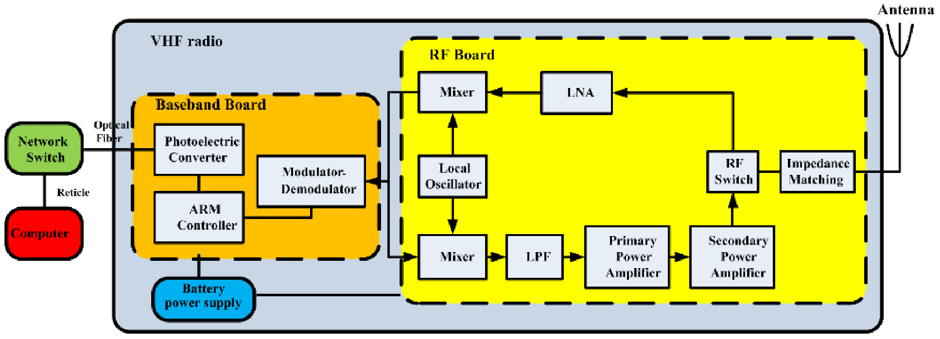
2.1. The VHF Wireless Communication System and Vulnerability Analysis

The energy contained in a HEMP environment is mainly concentrated below 100 MHz. Because the high frequency or very high frequency (HF/VHF) radio is within HEMP frequency range, the effects of function failure or performance degradation occurred often during the pulse illumination test [15,16]. As shown in Figure 1, a small prototype of a VHF electronic system with superheterodyne transceiver, consisting of antenna, RF board, baseband board, and computer, etc., was developed. The RF board consisted of transmitting channel and receiving channel [17]. The transmitting channel mainly contained a mixer, a low pass filter and primary and secondary power amplifiers. The receiving channel mainly contained a LNA and a mixer. A RF switch was used to control the channel selection for the transceiver, and the impedance matching was designed with L-C circuits to solve the impedance mismatch between antenna and RF circuits.
As the antenna was exposed to the outdoor environment, the antenna and the RF front end were the main front-door coupling channels. An electromagnetic pulse through the antenna system coupling induced pulse current, which entered the RF front end, transmitted pulse energy along the RF channel step-by-step, and impacted the RF electronic modules.
A PCI test was performed on the SUT with a HEMP double-exponential wave. The results demonstrated that the communication-receiving sensitivity of the SUT decreased, and the analysis of the effect mechanism demonstrated that it was all caused by the damage of the RF LNA component on the RF board [17]. Note that the RF switch had failed in previous tests due to its semiconductor materials and its proximity to the antenna port. However, its damage threshold is much higher than that of LNA based on test results. To assess the survivability and vulnerability of the electronic system, we focused more on the study of SUT performance degradation or functional failure under the impact of the lowest HEMP environmental strength, which is considered the worst case of the SUT.
A pulse illumination test was also performed on the SUT using a vertically polarized bounded wave simulator. The results of the illumination test verified the conclusions obtained in the PCI test. The test configurations of the PCI and pulse illumination tests are illustrated in Figure 2. In PCI tests, the PCI generator uses coaxial cable directly connected to the RF port of the SUT as the output line. After each test, the antenna is reconnected to the SUT for communication debugging [18].
In addition, the effect of LNA damage often occurs in wireless radios excited by a HEMP. Therefore, the main coupling channel of the SUT is its RF front-end, and its vulnerable component is LNA when the SUT is exposed to HEMP.

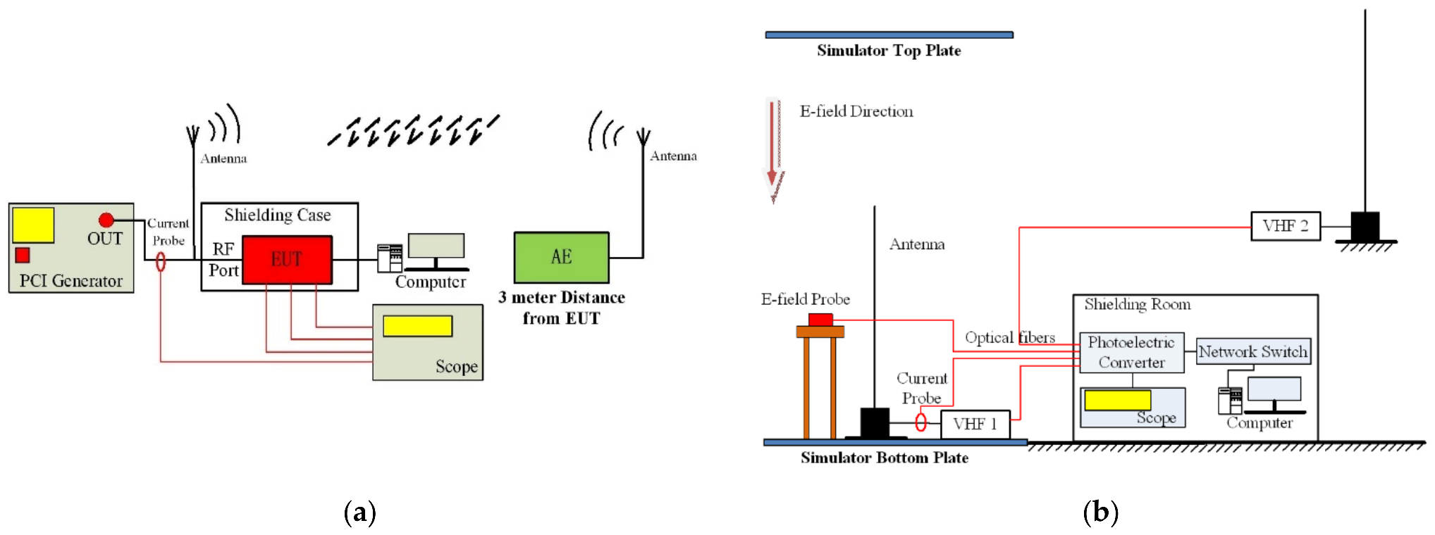
2.2. Problem Description

It is difficult to obtain sufficient experimental data for the fitting of damage threshold distribution by conducting a system-level illumination test. On the one hand, it is limited by the number of samples of the SUT, and on the other hand, it is limited by many factors such as the instability of the excitation source in the illumination test and the step interval of the excitation source output. After determining the vulnerable components, how to obtain the threshold distribution curve by carrying out a large sample PCI test on the vulnerable components for computing the system-level damage threshold distributions, the key problem to be solved was identified. Before solving this problem, we should establish the relationship between the component-level PCI waveform and the actual coupled response of the pulse illumination test. Acknowledging that the effect phenomenon and mechanism of vulnerable components are similar to the damage effect and mechanism of the system-level illumination test allowed us to establish their equivalent relationship. The major difference between these two environments is that the component-level PCI waveform can be selected from the simple and typical standard wave, such as a square wave, with different pulse width. The coupled response reached the vulnerable device-under-test (DUT) port in the pulse illumination test is so complex that is hard to simulate it with pulse generating technology. How to utilize vector norm theory and mechanism analysis to establish their equivalence is a key issue, which is an electromagnetic parameter selection problem.
Therefore, simplified standard waveforms and a typical HEMP conduced waveform are selected in this paper for the PCI tests of the vulnerable component LNA. They are waveforms with square waves of multiple pulse-widths and double exponential waveforms with 20 ns/500 ns, respectively, for carrying out a PCI test. The correlation between waveform parameters and effect mechanism are studied using vector norm theory.

3. Component-Level PCI Tests of LNA and Data Analysis

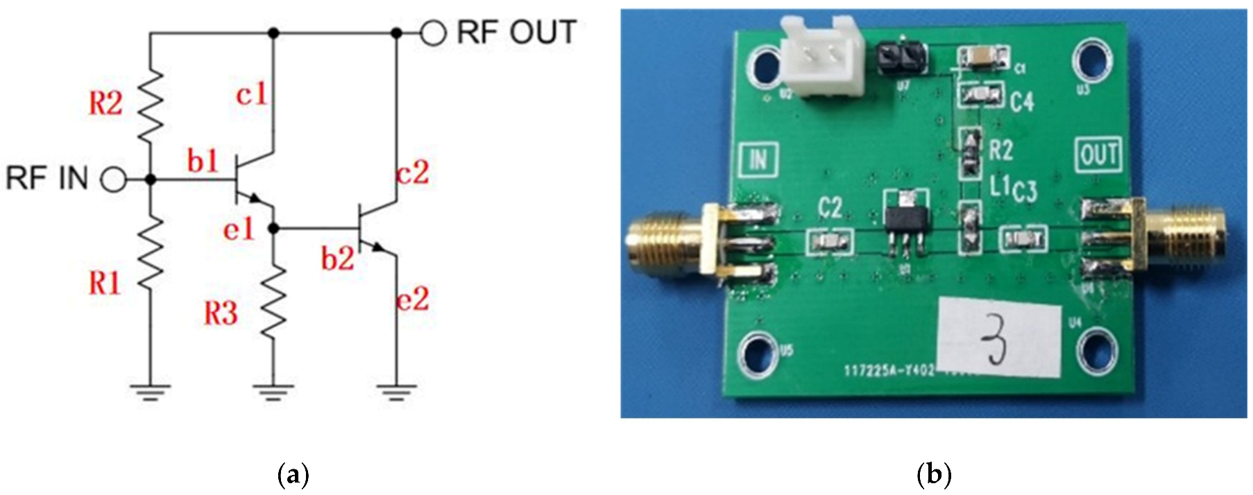
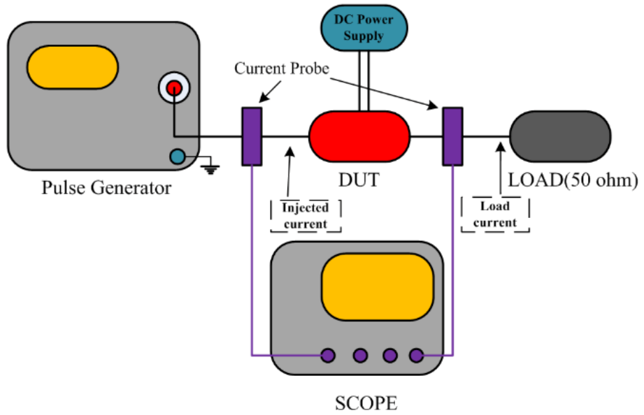
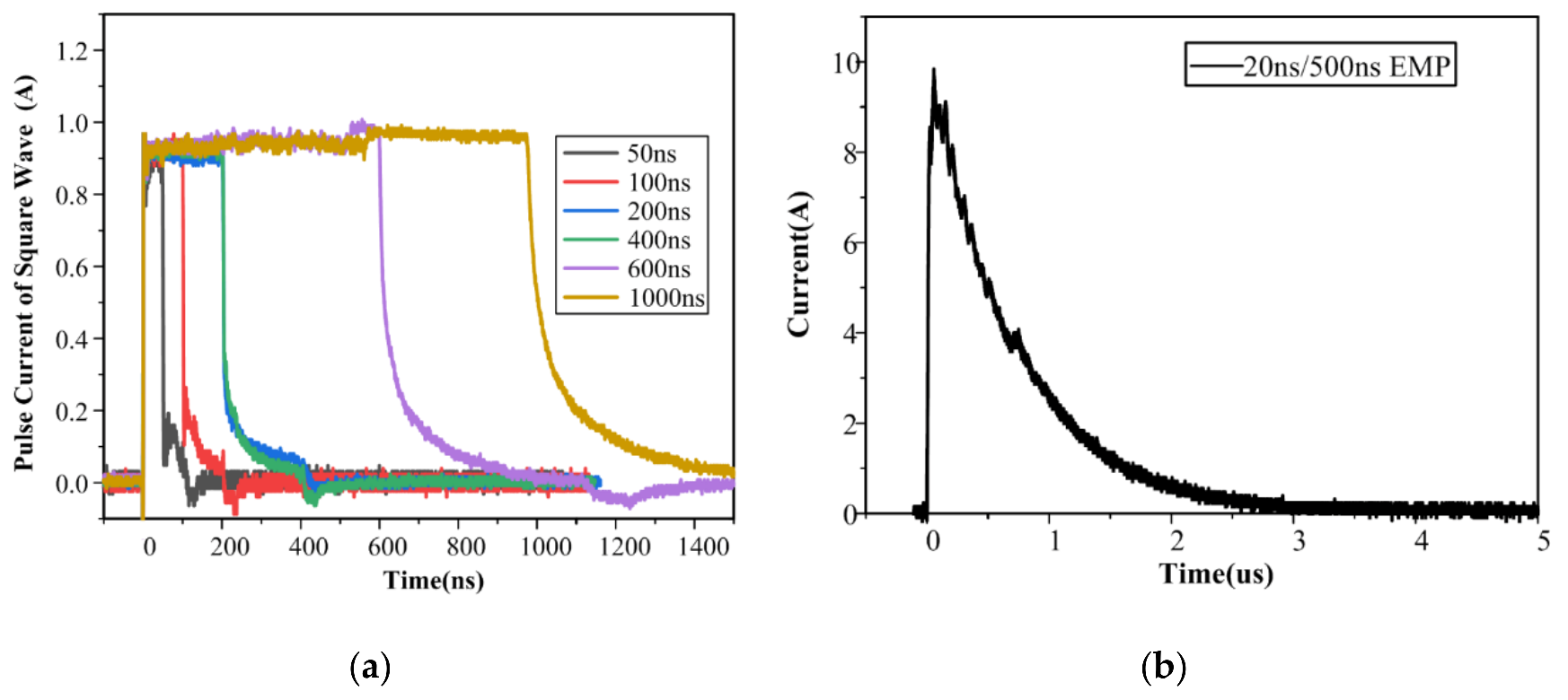
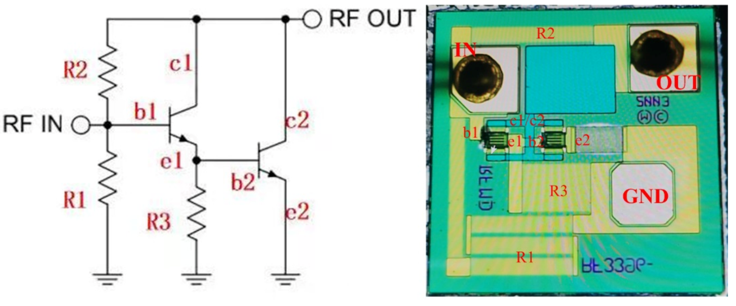
3.1. The LNA and the PCI Test Method

The model of the RF LNA used in the SUT is RF3376 with materials belonging to GaAs HBT [19]. The circuit of RF3376 is a two-stage amplifier cascade structure as shown in Figure 3a, which is packaged in an RF integrated chip. Based on the impedance matching and bias circuits provided in the manufactures’ datasheet, we designed a test board as the DUT for the component-level PCI test as illustrated in Figure 3b. RF3376, which is suitable for frequency range DC~6 GHz with signal gain factor 22 dB, and 5 V DC power supply, is widely used in wireless communication products due to its low cost.
This subsection describes the test configuration and waveforms injected in the RF3376 component-level PCI test. The PCI test configuration is shown in Figure 4. Injected current and load current are monitored with two coaxial current probes, respectively, and a 50 ohms load is connected to the DUT output port. The injected pulse generated by the pulse generator are square wave with different pulse-widths of 50/100/200/400/600/1000 ns, and double exponential pulse with 20 ns rising time and 500 ns pulse width. For each DUT sample, the injection voltage level is changed from low to high until the effect appears. The standard output waves of a pulse generator with ideal loads are calibrated as shown in Figure 5. The standard injected waves occur when the square pulse generator is connected to 50 ohm loads and the HEMP pulse generator is connected to 0 ohm loads respectively.
The criterion for determining whether the effect phenomenon occurs in a PCI test is based on the shape of the injection waveform. PCI tests on RF3376 have shown varying degrees of degradation in the amplifier gain performance when the injection voltage level is greater than 150 V, indicating that the component is very vulnerable. In the actual pulse illumination test, the pulse voltage loaded to the RF port of the SUT through antenna coupling the HEMP can reach several kilovolts, and the RF3376 is completely damaged. Therefore, this paper focuses on the phenomenon of complete damage effect under the harsher high voltage level.
Furthermore, when the injection voltage level is equal to or higher than the RF3376 complete damage threshold, the injection waveform shape is completely different from that of the injection waveform below the failure threshold. Therefore, we take the injection waveform of this typical shape as the failure criterion and believe that once this type of waveform appears, complete damage will occur in the DUT. The comparison of the injection waveforms higher and lower than the threshold waveform of the complete damage effect are shown in Figure 6.
As illustrated in Figure 6a, for a double-exponential wave, the injection waveform shape is very close to the standard injected pulse connected to a short-circuit load when complete damage occurs. Figure 5b shows that there is a short-circuit channel to GND inside the DUT, which makes the impedance of the DUT’s input port close to 0 Ohms. The oscillation of the injection waveform when only gain loss occurs can also demonstrate the input port of the DUT has certain impedance characteristics, and the injection waveform presents the impedance mismatch between pulse generator and the DUT.

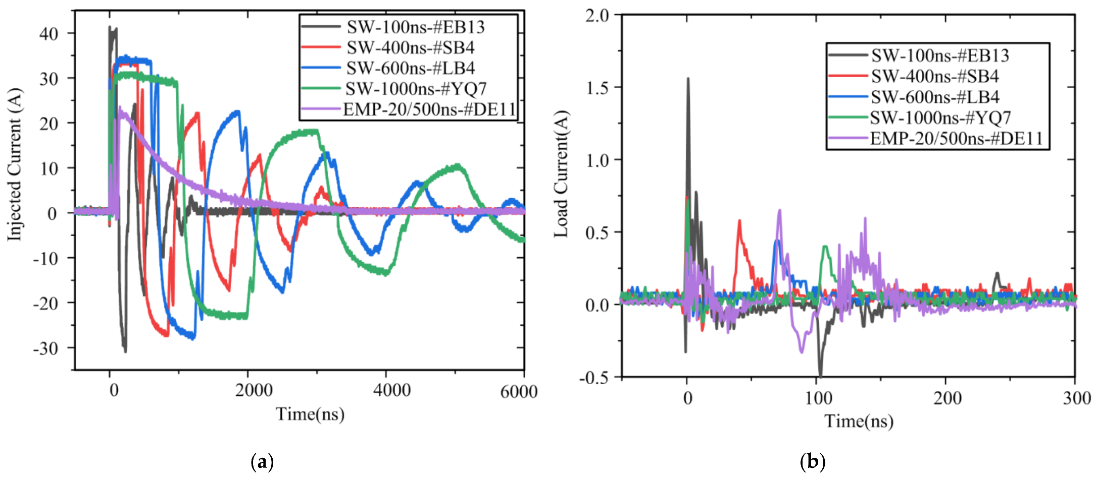
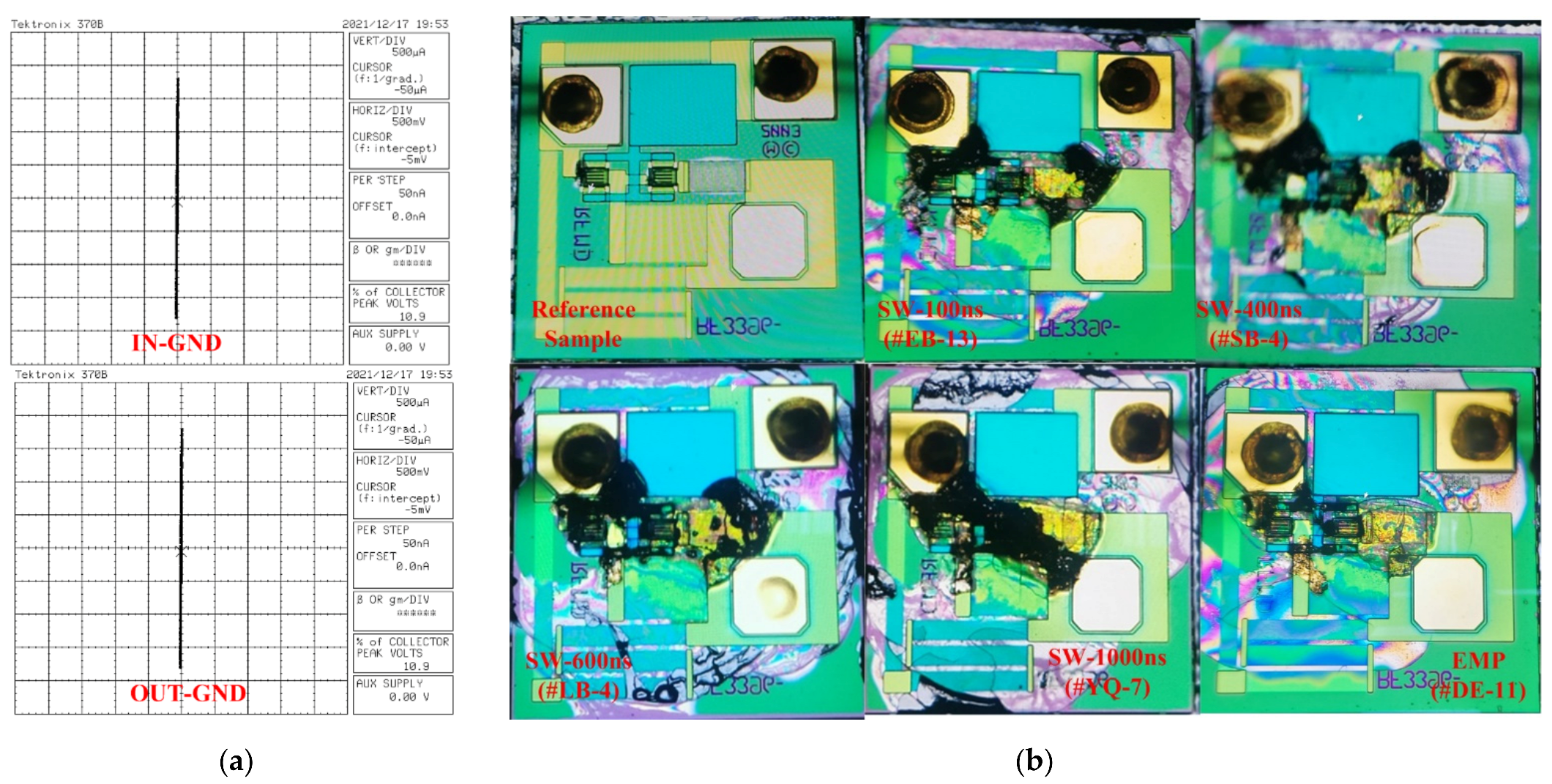
3.2. Result after PCI with Different Pulses

The experiment, showed a consistency of test data of all samples in each injection environment, which is convenient for statistical analysis. Table 1 and Figure 7 show some test data and measured waves under typical injection environment, respectively. According to Table 1, the load current, that is, the residual pulse current after passing through the DUT is at an average level of 1 A. With the comparison of peak values for injected wave and residual wave (Figure 7), it can be conjectured that a ground discharge channel exists in the DUT. The main pulse energy entering the DUT from the pulse source is released along the ground discharge channel into the ground, protecting the back-end load from pulse impact, which can be seen from the injection waveforms in Figure 7. The shapes of the square wave and the double exponential waveform also verify the near-short-circuit ground channel in the DUT. After the functionality test, these samples (DUT) suffered very serious destruction.
The major damage modes of semiconductor devices include open circuit and short circuit. Due to the different physical mechanism, the location of the damage point and its severity will influence the I–V characteristics and performance indicators such as gain or noise factor, etc., for the device. In this paper, destruction can be considered as very serious damage, and performance degradation like gain decline can be considered as slight damage.
Due to the difference in electromagnetic properties of device materials, they may have different electromagnetic sensitivities to pulse peak value, pulse integral energy, rate of rising edge and rectification impact [1,20]. Vector norm theory has been widely used to characterize EMP waveform characteristics and effect mechanism, such as the U.S. military standard MIL-STD 188–125, IEC standard 61000-4-33 and other international specifications and standards [20,21].
Vector norm theory generally adopts mathematical vectors or matrices to express its features and properties, which are defined as:
f ( t ) p = f ( t ) p d t 1 / p
Therefore, f(t) is the injection current waveform of the INPUT port of DUT. As shown in Table 2, 2-norm and -norm are used to study the electromagnetic sensitivity characteristics of the DUTs, which represent the energy and peak value of the injected current wave respectively.
The blue and red scatter points in Figure 8 are the sample failure threshold data represented by -norm and 2-norm, respectively, and the trend curve reflecting the correlation between failure threshold and pulse width is obtained by the fitting method. When the pulse width is less than or equal to 200 ns, the -norm value used to represent the current peak value is similar, indicating that the electromagnetic sensitive parameter leading to the effect is mainly the current peak value, and the corresponding effect mechanism is mainly breakdown. When the pulse width is located in 800 ns to 1000 ns, the trend of the red curve shows that the 2-norm representing energy tends to be stable, indicating that the electromagnetic sensitive parameter is mainly energy, and its effect mechanism is mainly burnout. With the increase of pulse width, the trend of -norm falls and 2-norm rises, showing that energy plays a more important role than peak value. This is the transition zone from peak to energy, which is called the transition zone of electromagnetic sensitive parameter competition failure. Therefore, based on this discovery of the effect laws, the pulse-width zone is distinguished and includes -norm dominating, 2-norm dominating and competitive failure dominating regions, respectively.

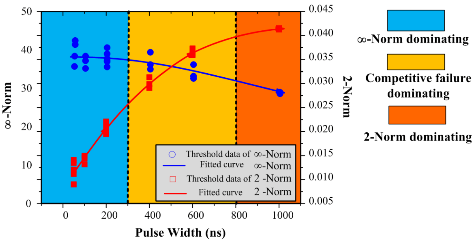
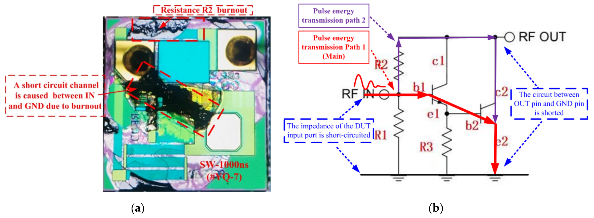
4. Mechanism Analysis on the Damage of the LNA

4.1. Mechanism for the Damage of the LNA

In this subsection, electrical parameter tests of I-V characteristics and optical microscopic analysis are performed on the damaged samples. Figure 9 shows a schematic diagram of the circuits in the RF3376. The amplifier consists of two GaAs BHT transistors that are cascaded with a common collector. The RF signal reached the receiver, entered into DUT through the RF IN port and was amplified by the two-stage amplifier, before outputting at the RF OUT port. The RF IN port was selected as the injection port in the PCI tests, and the RF OUT port was followed by a 50 ohms standard load.
In each injection environment, a typical damaged sample was selected for comparative analysis. As shown in Figure 10a, the pin pairs of IN-GND and OUT-GND of all damaged samples show short-circuit low resistance characteristics, indicating that short-circuit channels appeared inside due to pulse impact. As shown in Figure 10b, the main damaged parts of all the damaged samples are the two cascaded transistors of DUT. According to the damage degree, as the pulse width of the injection waveform increases, the burning degree of the transistor becomes more serious, indicating that the energy norm (2-norm) has a more obvious influence on the device destruction with the increase of the pulse width. These results verify the effect laws obtained in Section 3. However, in the study of the semiconductor device damage mechanism, the low resistance channel always reflects damage induced by the breakdown effect of DUT, which causes an instant increasing pulse current that leads to the burnout. Therefore, as an intermediate process, it is difficult to find evidence of the breakdown effect in samples with a serious degree of burnout.
The sample #YQ-7 (Pulse width 1000 ns) with the most serious damage degree was taken as an example to study the short-circuit channel caused by pulse impact, as shown in Figure 11. The two transistors suffered the most serious damage. After the pulse energy entered the RF IN port, it reached the signal ground GND along B1 → E1 → B2 → E2, then forming the main pulse transmission channel 1, whose material was carbonized and presents a short-circuit characteristic. In addition, the bypass R2 resistor burned out, forming pulse transmission channel 2. The appearance of pulse channel 1 leads to short-circuit characteristics of RF IN and GND pins, and the pulse channel 2 and the burnout of PN junction of the first-stage transistor leads to short-circuit characteristic of RF OUT and GND pins, which agrees with the test results of I–V characteristics.

4.2. Waveform Equivalence and EM Parameter Determination

According to Figure 10b, the damage degree of the EMP environmental damaged sample #DE-11 is the lightest damaged degree in the PCI test, lower than the damage result of the square wave with 100 ns pulse width. Based on the Figure 7 injection waveform test results, due to the impedance mismatch caused by the short-circuit feature of the damaged DUT port, the output amplitude of the square-wave pulse generator became huge with a long-attenuated oscillation period, which will carry powerful energy to impact the DUT. However, the output of the EMP pulse generator will become close to the standard double-exponential wave when the DUT port is in short-circuit status. According to the difference of the wave shapes, the energy carried in the square-wave pulse is far greater than a double-exponential wave, which is largely responsible for the effect difference between the practical environment waveform and the standard simplified waveform.
With the same pulse width, we can see the energy carried in a square wave and that its impact on RF3376 is significantly higher than the 20 ns/500 ns EMP wave. If the square wave with the same pulse width as the environment wave, is selected as the injected wave instead of the actual coupled environment wave, it will be able to obtain harsher results. However, whether to choose square wave as injection waveform depends on the actual test requirements.
According to Figure 10b, we believe that the effect caused by a double exponential waveform can be approximately equivalent to the square wave environment with 100 ns pulse width for RF3376. As demonstrated in Figure 7a, the 2-norm of the test data of 100 ns square wave and double exponential wave are calculated at 0.0172 and 0.0156, respectively, and the numerical results are similar and at the same level. Based on the analysis results of norm theory and effect mechanism, 20 ns/500 ns double exponential waveform is equivalent to 100 ns square pulse waveform for the RF3376 component. From pulse-width regions divided in Figure 8, the electromagnetic sensitive parameter region of RF3376 is the -norm dominant region, and the electromagnetic sensitive parameter of RF3376 under the 100 ns square-wave injection environment is the current peak.

5. Conclusions

To utilize a component-level PCI test to assist in system-level tests for damage threshold distribution, it is necessary to study the electromagnetic sensitivity characteristics of the vulnerable electronic components. First, a small electronic system was developed as the research object, and the RF LNA was diagnosed as a vulnerable component by a PCI and pulse illumination test. Then the PCI tests of RF3376 were carried out with square waveforms of different pulse widths and double exponential waveforms of typical a HEMP conducted environment. The action rules of electromagnetic sensitive parameters were obtained by using norm theory. The effect mechanism and damage path were determined by electrical parameter and optical microscopic analysis. Based on the results of norm and mechanism analysis, the equivalent square wave of the double exponential waveform and the electromagnetic sensitive parameter of square-wave injection were determined. The main conclusions are as follows:
According to the laws of the damage threshold curves represented by norms varying different square waves, the electromagnetic parameter action is divided into three regions, called -norm, 2-norm and competitive failure dominating regions. The -norm dominant region indicates that the peak value of the injection waveform plays a major role in the damage effect; 2-norm indicates the energy; and the competitive failure region indicates that multiple electromagnetic sensitive parameters such as peak value and energy jointly play a role in the damage effect.
The electromagnetic damage effect of RF3376 is mainly caused by the burning of two transistors in a cascade relationship, forming a pulse energy transmission channel from the component input port to the signal ground GND. The pin pair IN-GND and OUT-GND of the DUT are short-circuited due to the short-circuit impedance characteristics of the channel. The effect mechanism provides the explanation of the injection waveform shape when DUT is completely destroyed and verifies the test results of I-V characteristics.
By analyzing the norm results and damage mechanism of a double exponential environment waveform and a square waveform, the 100 ns square waveform can be determined as the equivalent injection waveform of 20 ns/500 ns double exponential waveform. As a 100 ns square wave is in the -norm dominating region, the pulse peak value of injected current is determined as the electromagnetic sensitive parameter for square-wave PCI tests of RF3376.
In future work, the equivalence of the system-level pulse illumination test and the component-level PCI test based on a simplified injection wave will be investigated further to solve the feasibility problem of using the component-level injection test with large sample size to supplement the system-level test with small sample size.

Author Contributions

Conceptualization, C.D. and C.M.; methodology, C.D. and W.F.; validation, W.F. and Z.C.; formal analysis, Q.H., C.M. and Z.C.; investigation, D.X. and Q.H.; resources, X.N.; data curation, D.X.; writing—original draft preparation, C.D. and D.X.; writing—review and editing, Q.H. and W.F.; supervision X.N.; project administration, C.M.; funding acquisition, W.F. All authors have read and agreed to the published version of the manuscript.

Funding

This research was funded by [National Natural Science Foundation of China] grant number [No. 92166111].

Conflicts of Interest

The authors declare no conflict of interest.

References

  1. Giri, D.V.; Hoad, R.; Sabath, F. High-Power Electromagnetic Effects on Electronic System; Artech House: London, UK, 2020; pp. 1–50. [Google Scholar]
  2. Giri, D.V.; Tesche, F.M. Classification of intentional electromagnetic environments (IEME). IEEE Trans. Electromagn. Compat. 2004, 46, 322–328. [Google Scholar] [CrossRef]
  3. Mao, C.; Canavero, F. System-level vulnerability assessment for IEMI: From fault tree analysis to Bayesian networks- Part I: Methodology framework. IEEE Trans. Electromagn. Compat. 2016, 58, 180–187. [Google Scholar] [CrossRef] [Green Version]
  4. Mao, C.; Canavero, F.; Cui, Z.; Sun, D. System-level vulnerability assessment for IEMI: From fault tree analysis to Bayesian Networks-Part II: Illustration to microcontroller system. IEEE Trans. Electromagn. Compat. 2016, 58, 188–196. [Google Scholar] [CrossRef] [Green Version]
  5. Cui, Y.; Zhang, Y.; Wang, Z.; Fu, H.; Mao, X. Interval statistic-based reliability analysis method on small sample hot test of satellite thruster. Appl. Math. Modeling 2018, 60, 581–591. [Google Scholar] [CrossRef]
  6. Zhang, S.F.; Yang, H.B.; Zhang, J.H. Reliability assessment methods with small-sample for device with only safe-or-failure pattern. Nucl. Power Eng. 2006, 27, 79–83. [Google Scholar]
  7. Dinkar, B.K.; Mukhopadhyay, A.K.; Chattopadhyaya, S.; Sharma, S.; Alam, F.; Machado, J. Statistical reliability assessment for small sample of failure data of dumper diesel engines based on power law process and maximum likelihood estimation. Appl. Sci. 2021, 11, 5387. [Google Scholar] [CrossRef]
  8. Bourinet, J.M.; Mattrand, C. Damage tolerance and reliability assessment under random Markovian loads. Procedia IUTAM 2013, 6, 123–131. [Google Scholar] [CrossRef] [Green Version]
  9. Bee, S.; Leferink, F. Vulnerability of remote keyless-entry systems against pulsed electromagnetic interference and possible improvements. IEEE Trans. Electromagn. Compat. 2016, 58, 1259–1265. [Google Scholar]
  10. Camp, M.; Garbe, H. Susceptibility of personal computer systems to fast transient electromagnetic pulses. IEEE Trans. Electromagn. Compat. 2006, 48, 829–834. [Google Scholar] [CrossRef]
  11. Pan, X.; Wei, G.; Lu, X.; Wan, H.; Fan, L. Equivalent simplification method of complex transient injection waveform. High Volt. Eng. 2017, 43, 1736–1744. (In Chinese) [Google Scholar]
  12. IEC 61000-2-10; Electromagnetic Compatibility (EMC): Part 2-10. Environment-Description of HEMP Environment-Conducted disturbance; IEC: Geneva, Switzerland, 1998.
  13. Ianoz, M.; Nicoara, B.I.C.; Radasky, W.A. Modeling of an EMP conducted environment. IEEE Trans. Electromag. Compat. 1996, 38, 400–413. [Google Scholar] [CrossRef]
  14. Baum, C.E. Norms and Eigenvector Norms. AFWL Math. Notes 1979, 63, 1–42. [Google Scholar]
  15. IEC 61000-2-9; Electromagnetic Compatibility (EMC): Part 2. Environment-Section 9: Description of HEMP Environment-Radiated Disturbance; IEC: Geneva, Switzerland, 1996.
  16. Coburn, W.O.; Nguyen, E.; Reyzer, R.J.; Mar, M.H. High-Altitude Electromagnetic Pulse Survivability Assessment of the Harris RF-3200 Transceiver; ADA258347; Harry Diamond Labs: Adelphi, MD, USA, 1992. [Google Scholar]
  17. Du, C.B.; Mao, C.G.; Sun, D.; Zhang, X. Effect Characterization and Modeling of RF Low Noise Amplifier for VHF communication System after HEMP PCI Test. In Proceedings of the 2020 IEEE MTT-S International Conference on Numerical Electromagnetic and Multiphysics Modeling and Optimization (NEMO) IEEE, Hangzhou, China, 7–9 December 2020. [Google Scholar]
  18. MIL-STD-188-125-2; High-Altitude EMP Protection for Fixed Ground-Based Facilities; United States Department of Defense: Washington, DC, USA, 1999.
  19. RF3376 Datasheet. Available online: https://html.alldatasheetcn.com/html-pdf/155390/RFMD/RF3376/95/1/RF3376.html (accessed on 28 December 2021).
  20. MIL-STD-188-125-1; High-Altitude EMP Protection for Fixed Ground-Based Facilities; United States Department of Defense: Washington, DC, USA, 1999.
  21. IEC 61000-4-33; Electromagnetic Compatibility (EMC): Part 4-33. Testing and Measurement Techniques-Measurement Methods for High-Power Transient Parameters; IEC: Geneva, Switzerland, 2005.
Figure 1. Diagram of electronic system with VHF transceiver.
Energies 15 01409 g001
Figure 2. Test configuration of SUT: (a) PCI test; (b) pulse illumination test.
Energies 15 01409 g002
Figure 3. RF3376 with GaAs HBT as DUT: (a) circuit structure inside the RF3376 chip; (b) the DUT for the PCI test.
Energies 15 01409 g003
Figure 4. Diagram of PCI test configuration.
Energies 15 01409 g004
Figure 5. Standard wave of PCI generator output: (a) square waves; (b) double exponential wave.
Energies 15 01409 g005
Figure 6. Injection waveform comparison of a HEMP conducted environment: (a) 20 ns/500 ns EMP; (b) square wave with 100 ns width.
Energies 15 01409 g006
Figure 7. Typical current waves of PCI test: (a) injected current waves; (b) load current waves.
Energies 15 01409 g007
Figure 8. Fitted curves of threshold data of -norm and 2-norm.
Energies 15 01409 g008
Figure 9. Schematic diagram of the circuits in the RF3376.
Energies 15 01409 g009
Figure 10. Effect mechanism detection result: (a) I-V characteristics; (b) Optical microanalysis.
Energies 15 01409 g010
Figure 11. Effect mechanism analysis: (a) explanation for burnout effect of Sample #YQ-7; (b) Pulse transmission paths.
Energies 15 01409 g011
Table 1. Measured data for PCI test.
Injected Wave
Parameter
Voltage Rank (V)Injected Current
Peak (A)
Load Current
Peak (A)
Sample
ID
Square wave
Pulse width 100 ns
120041.41.6#EB-13
Square wave
Pulse width 400 ns
100034.21.0#SB-4
Square wave
Pulse width 600 ns
100035.01.0#LB-4
Square wave
Pulse width 1000 ns
90031.21.0#YQ-7
EMP
20 ns/500 ns
140023.60.7#DE-11
Table 2. P-norms applied in this paper.
P-NormsMathematical
Expression
f(t)Physical MeaningApplication
2 0 f ( t ) 2 d t 1 / 2 Electric field, magnetic field, voltage, currentRoot of energy flowDevice is burnout due to overheat
f ( t ) max Electric field, magnetic field, voltage, currentPeak value
(absolute)
Digital circuit flip, switch or dielectric breakdown etc.
Publisher’s Note: MDPI stays neutral with regard to jurisdictional claims in published maps and institutional affiliations.

