
High Performance Single and Double Loop Digital and Hybrid PID-Type Control for DC/AC Voltage Source Inverters


Abstract
:1. Introduction
2. Double-Loop Control Architecture, PWM Strategies, and QCT Inverter Model
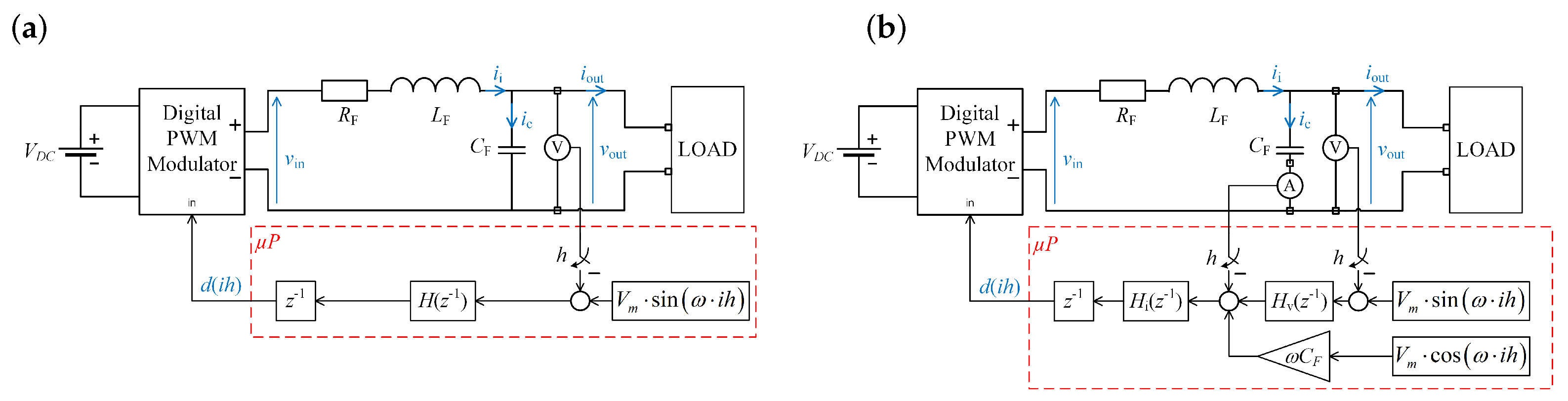
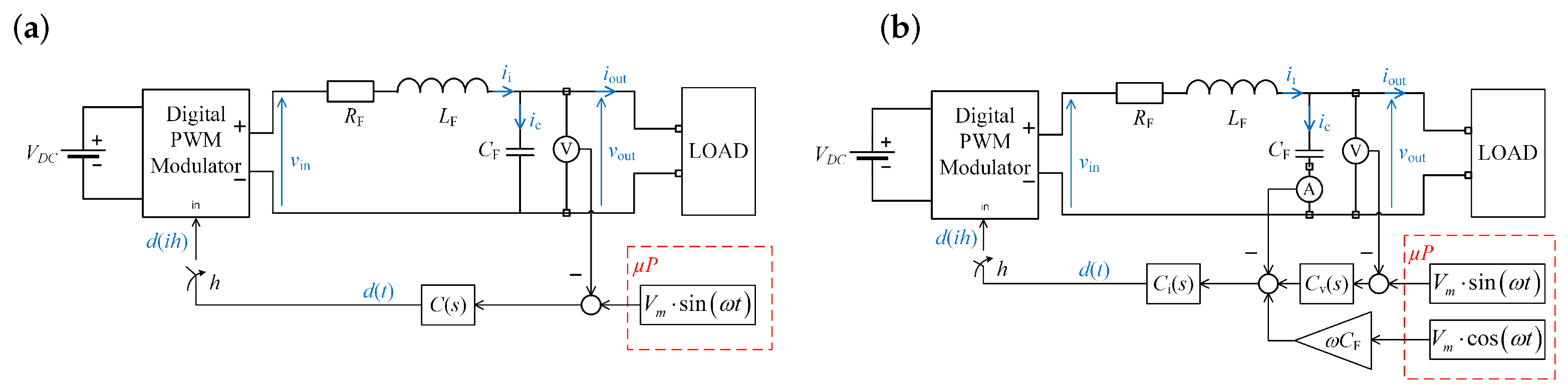
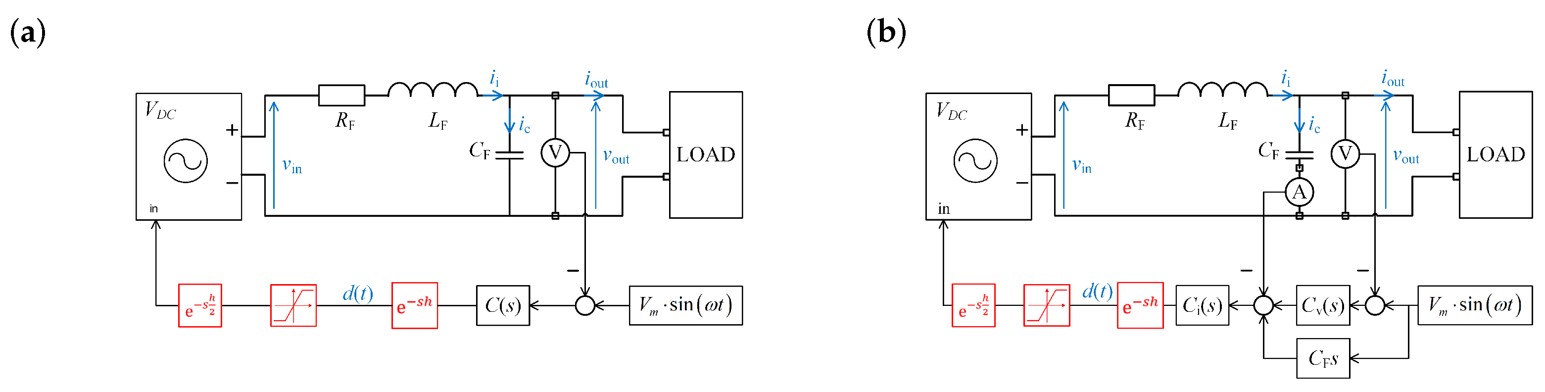
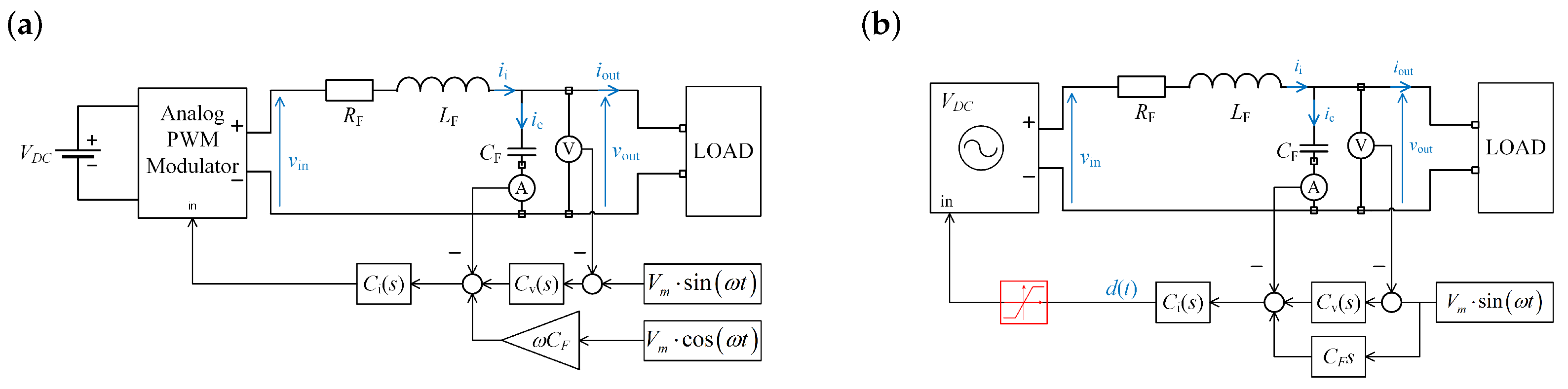
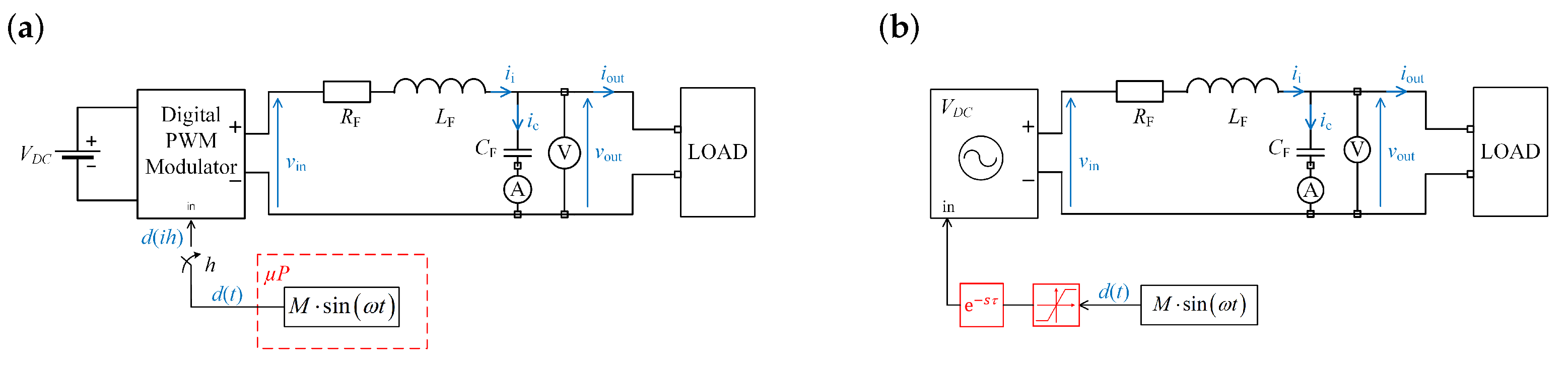
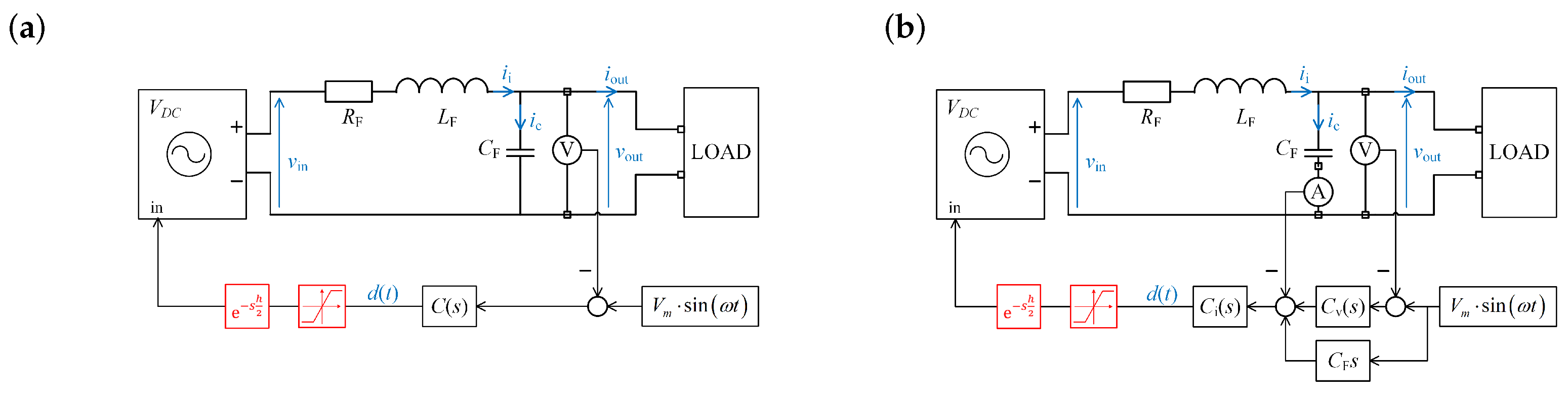
2.1. Double-Loop Control Architecture
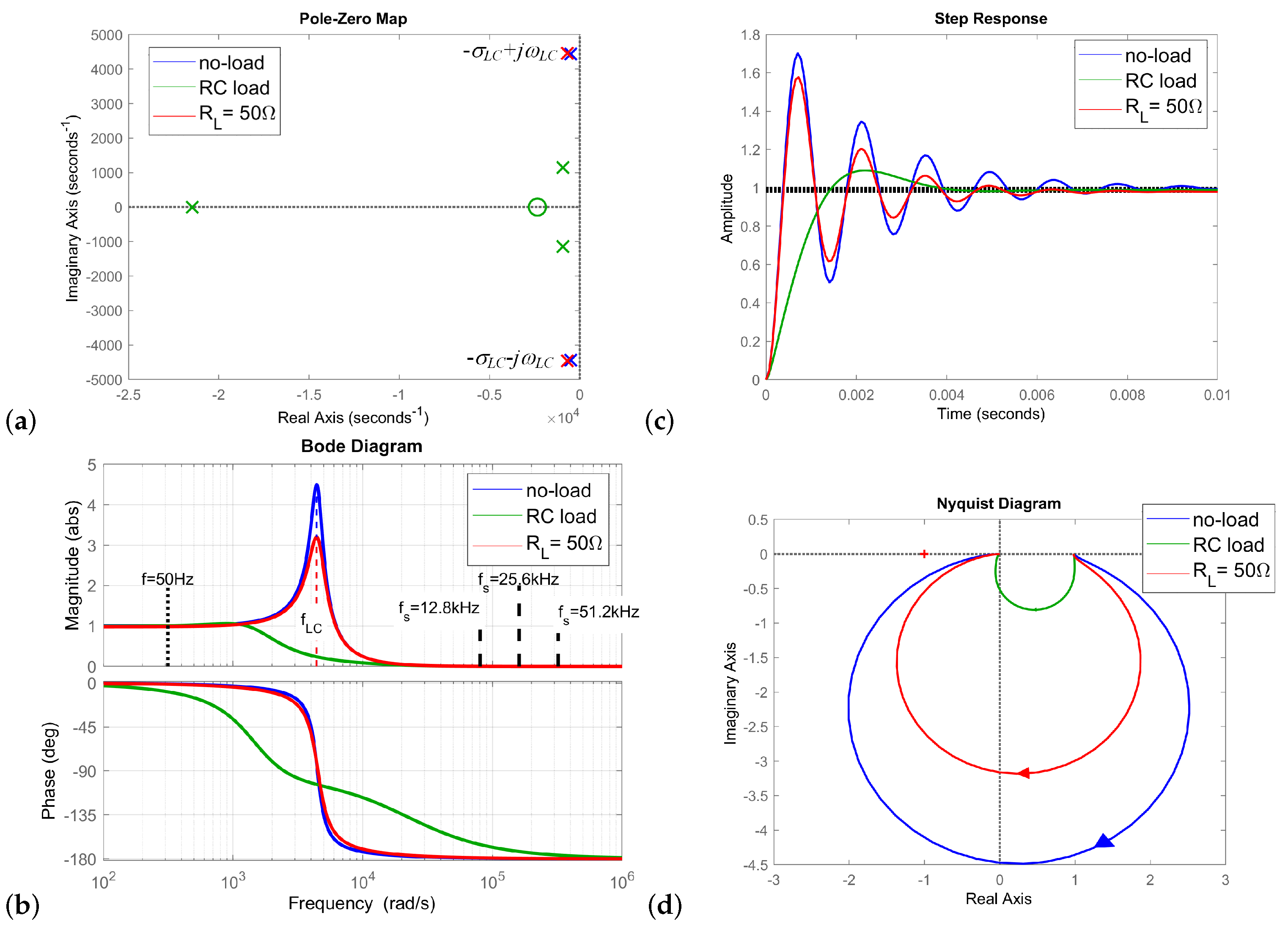
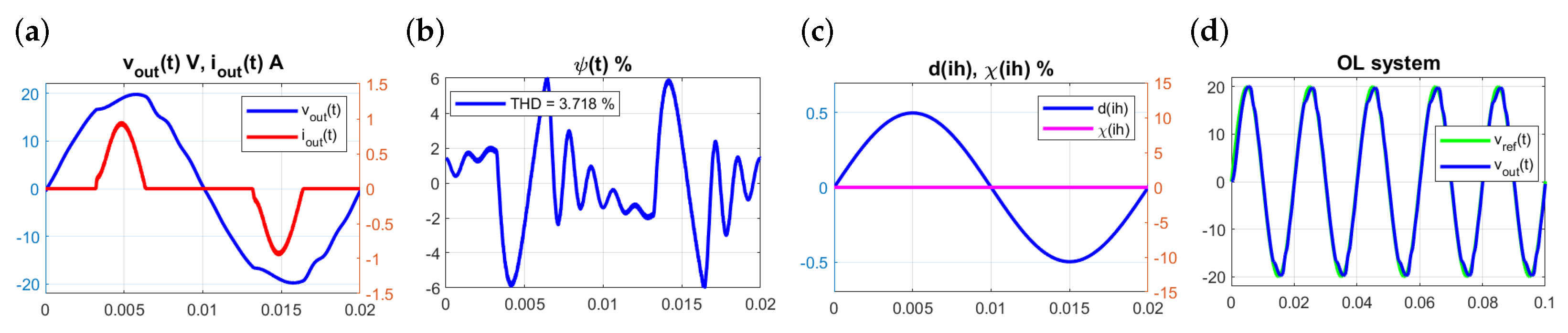
2.2. Preliminaries: Open Loop System
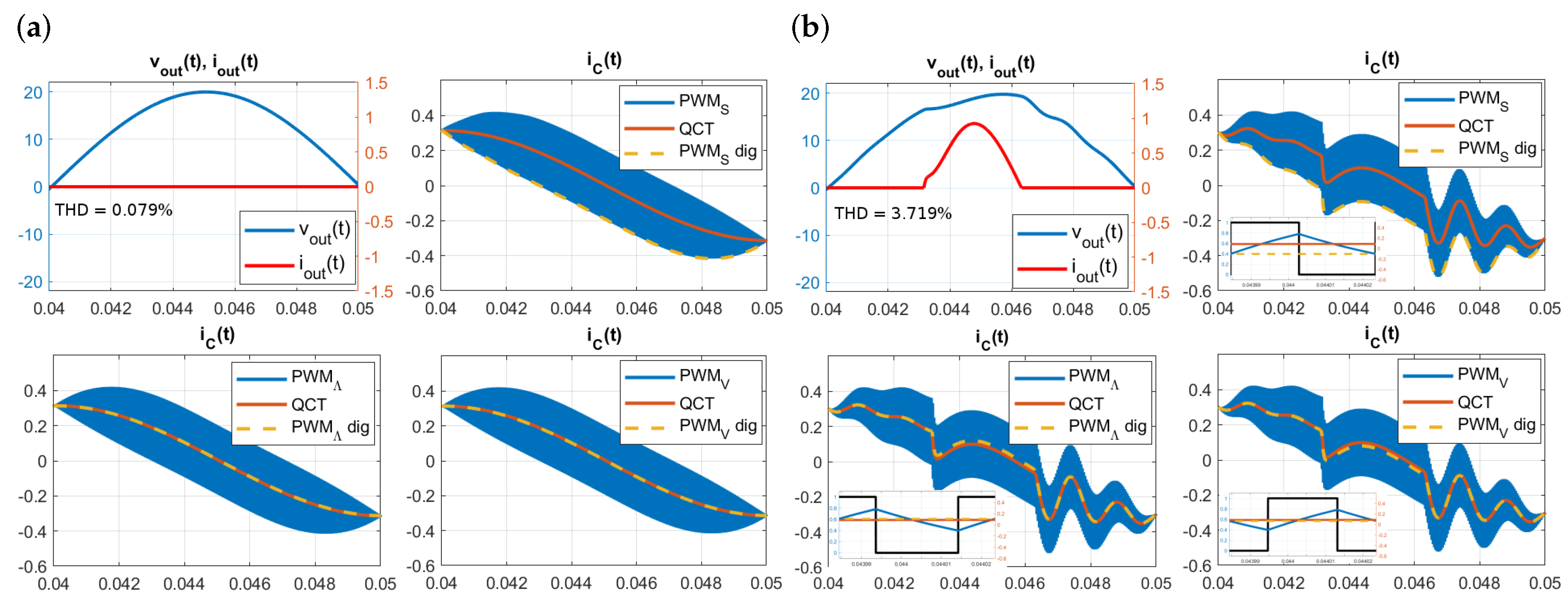
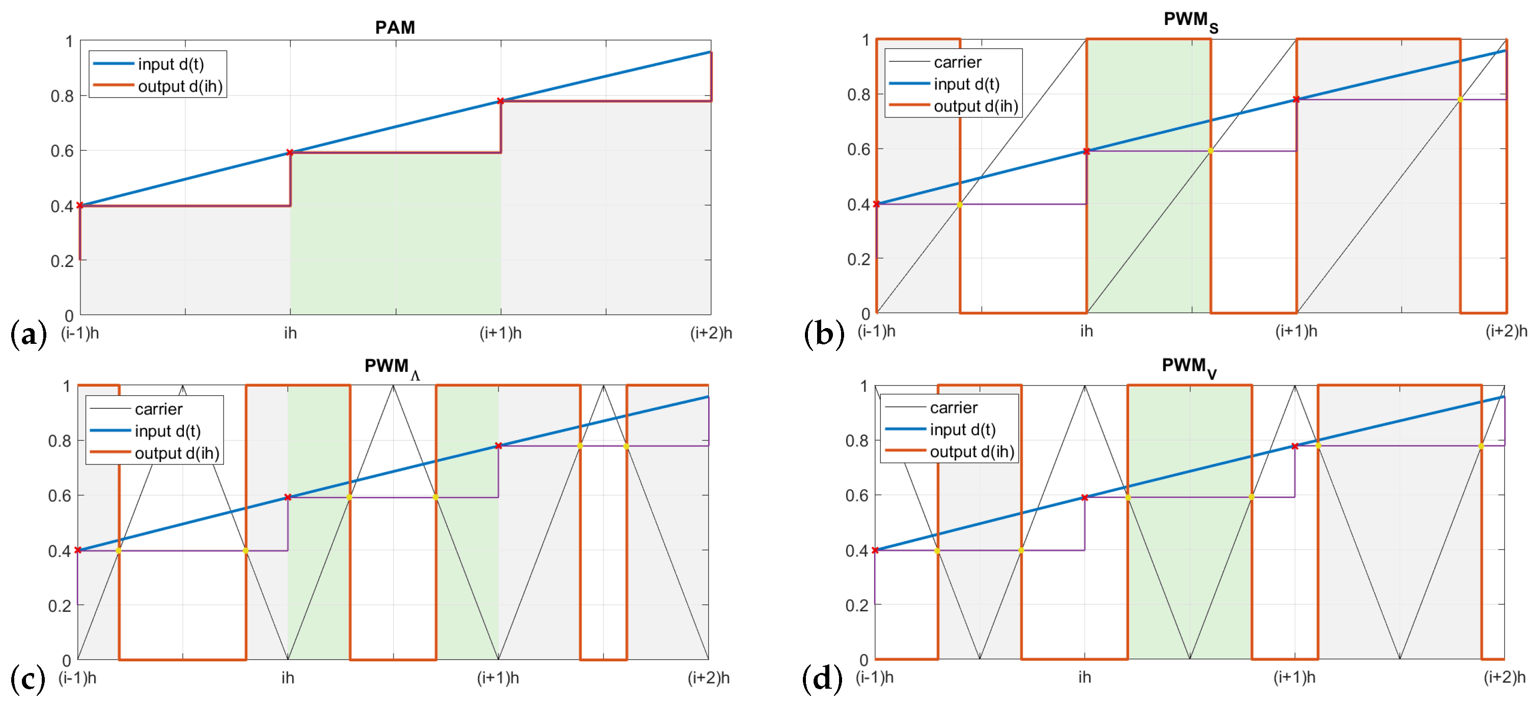
2.3. PWM Strategies
2.4. QCT Model of the PWM Controlled Inverter Output
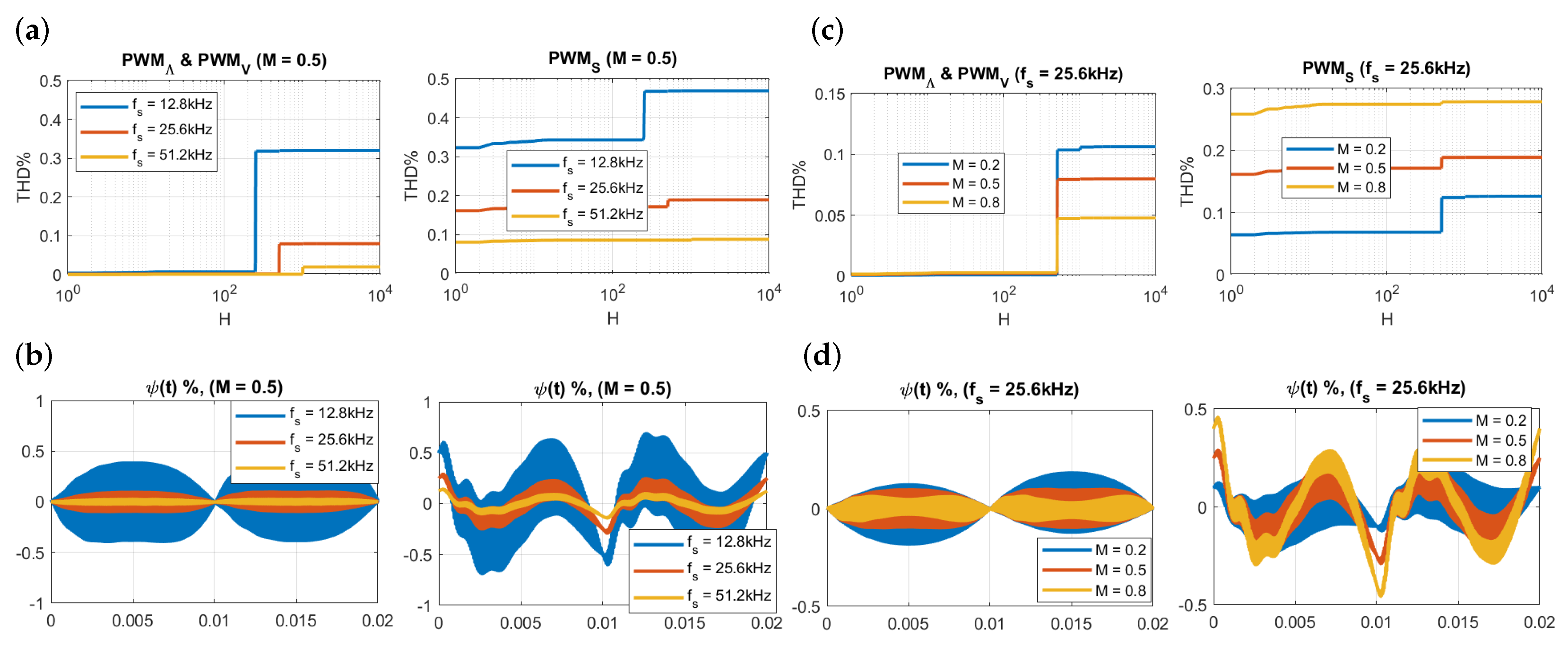
2.5. Distortion Functions and Total Harmonic Distortion-THD
2.6. Distortion and THD Function in Open-Loop VSI without Load
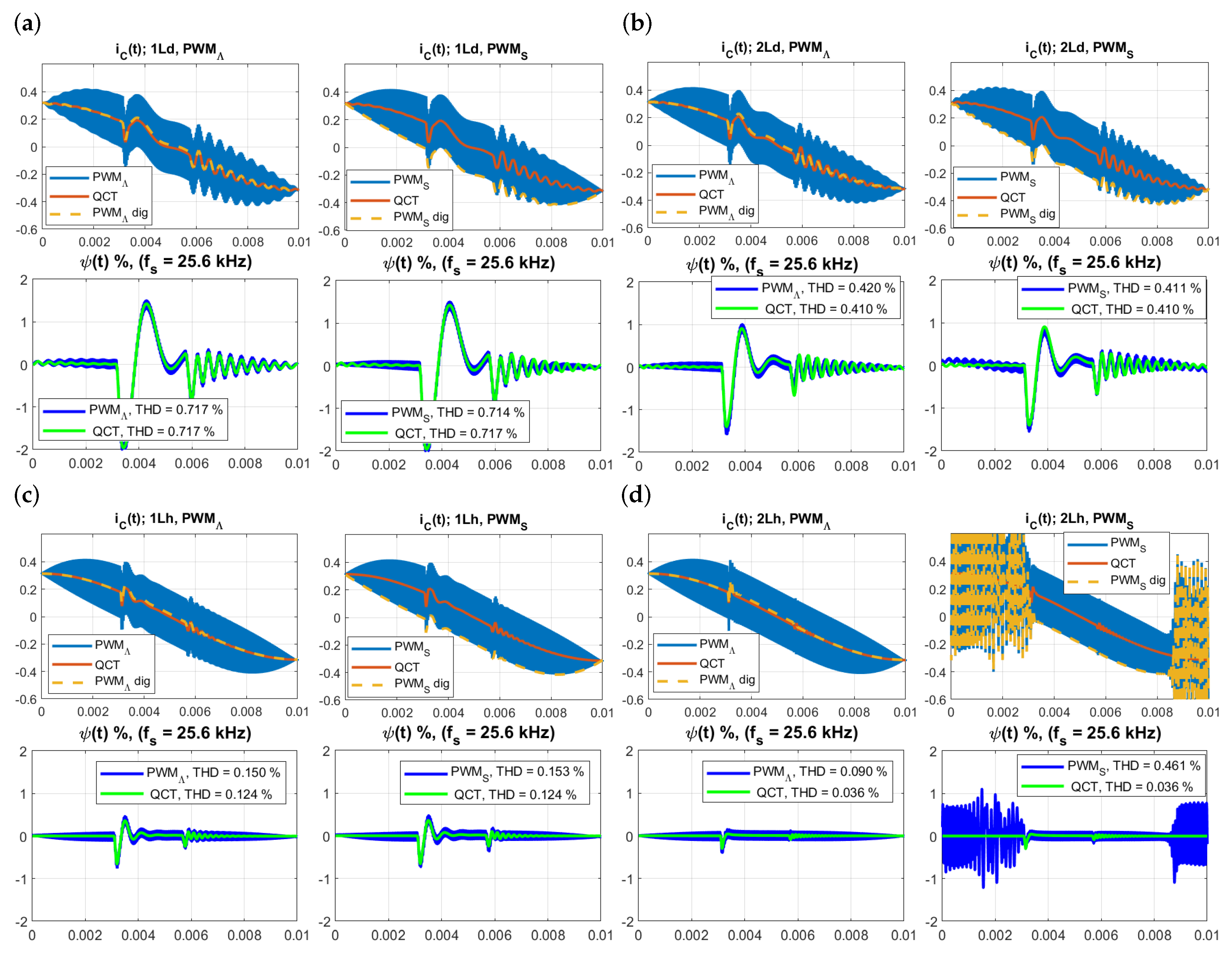
2.7. Capacitor Current and QCT Method
3. Control Systems
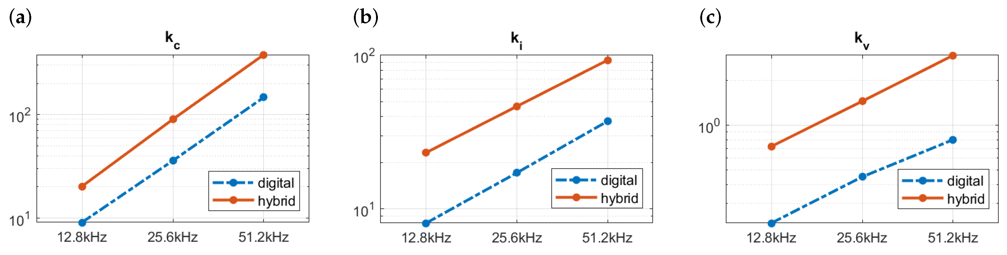
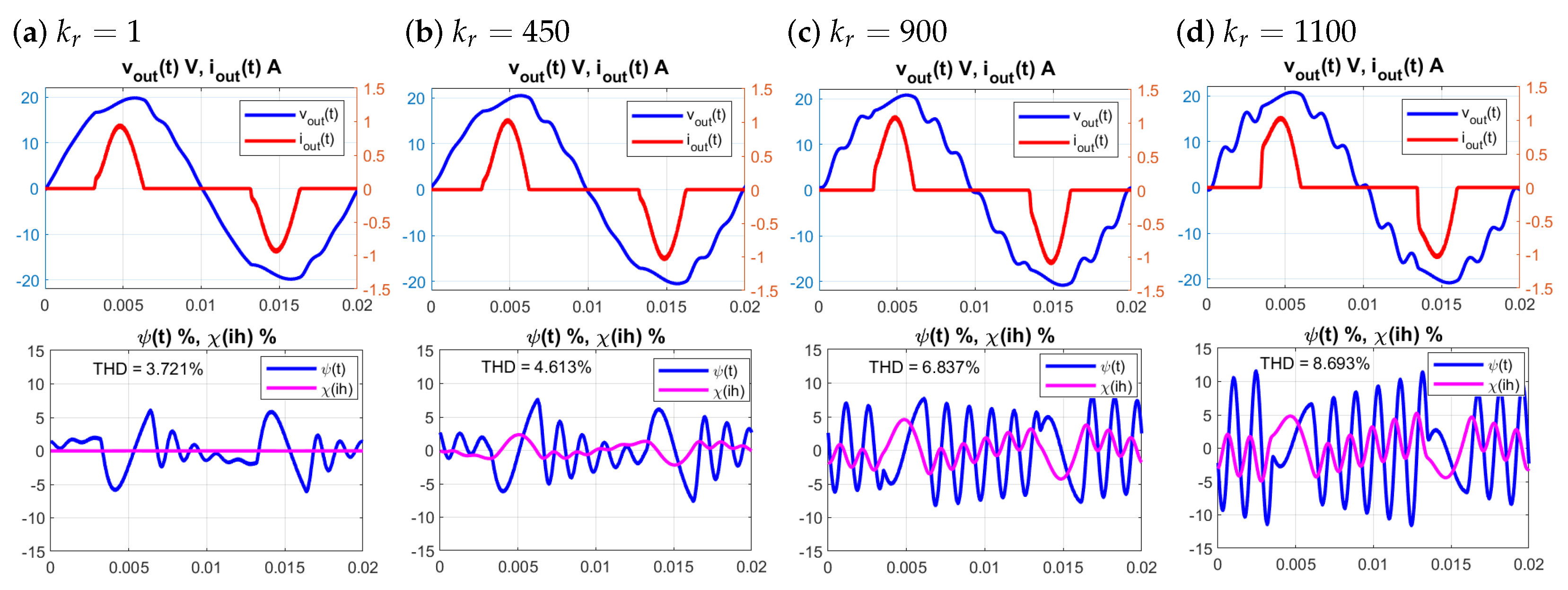
3.1. Remarks on the Loop and Controller Gains
3.2. Digital Control Systems
3.3. Hybrid Control Systems
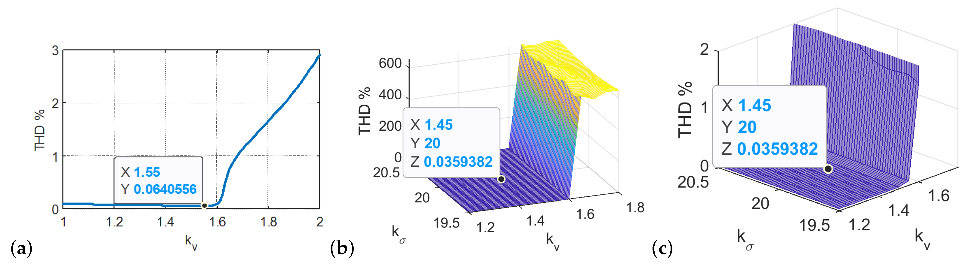
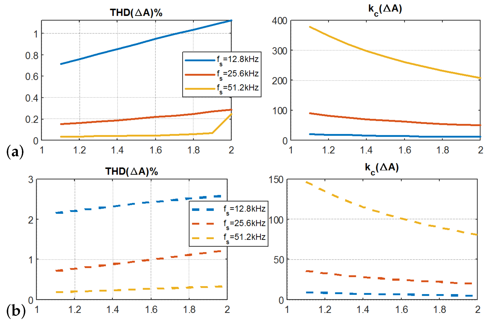
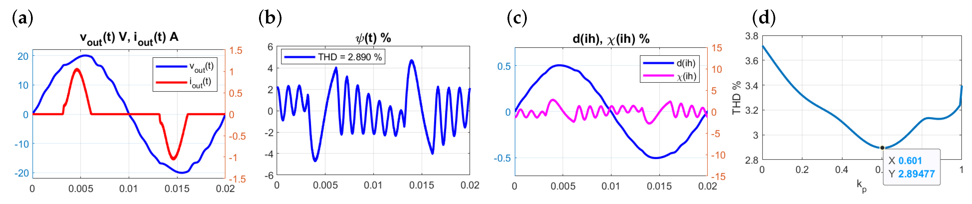
3.4. Optimal Controller Tuning
4. Simulation Results
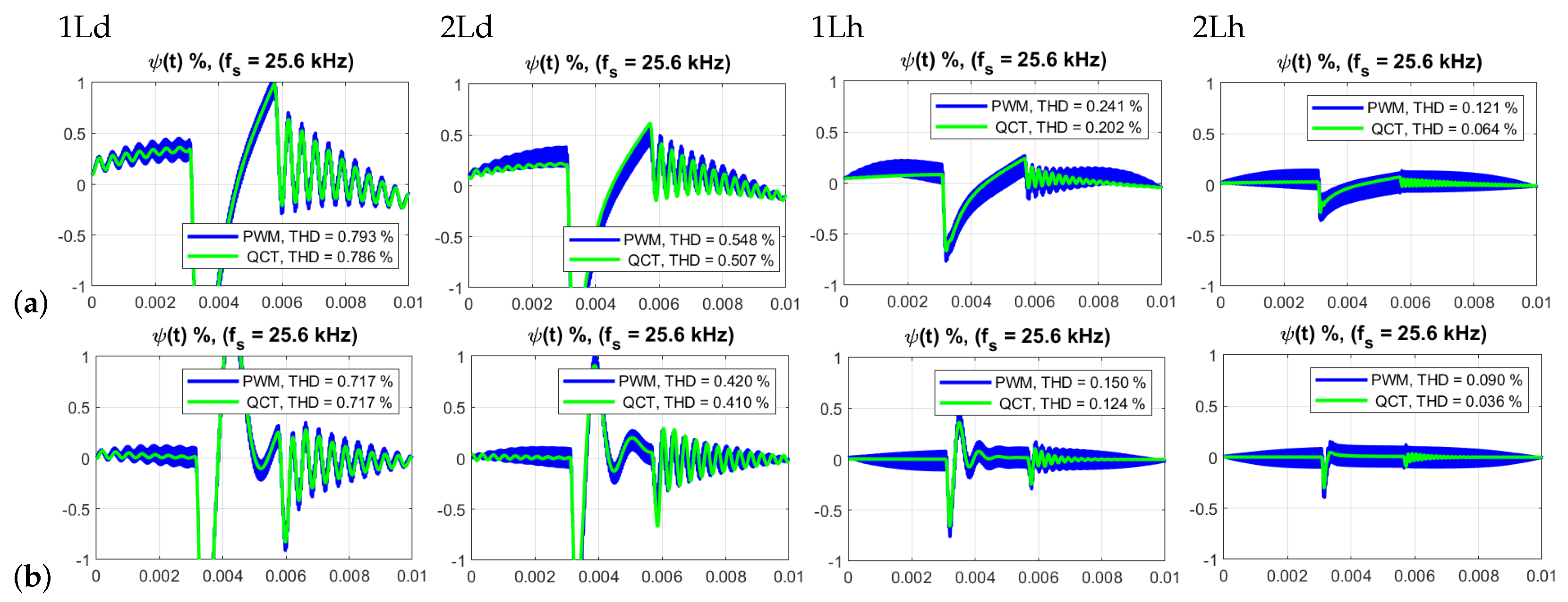
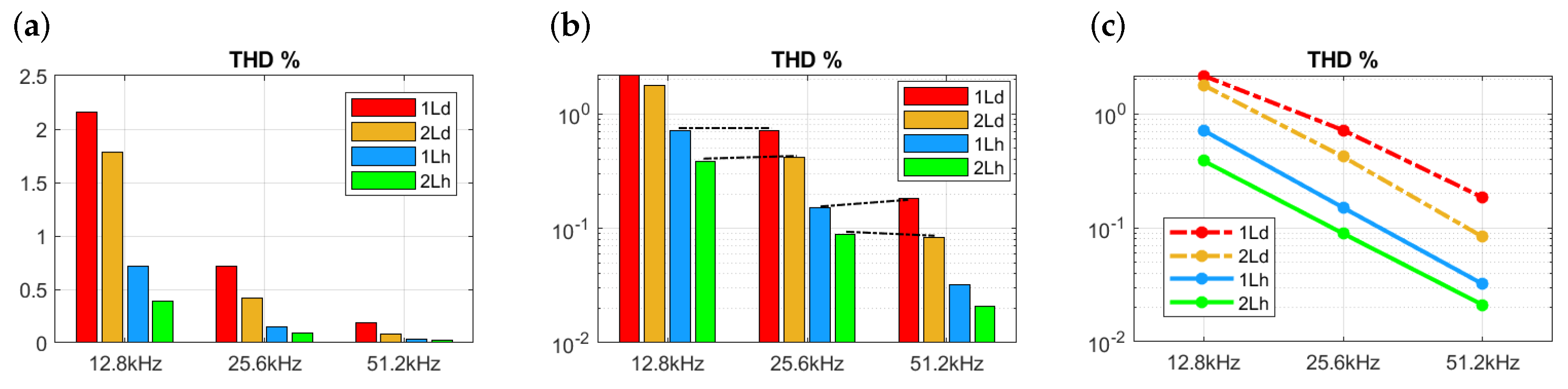
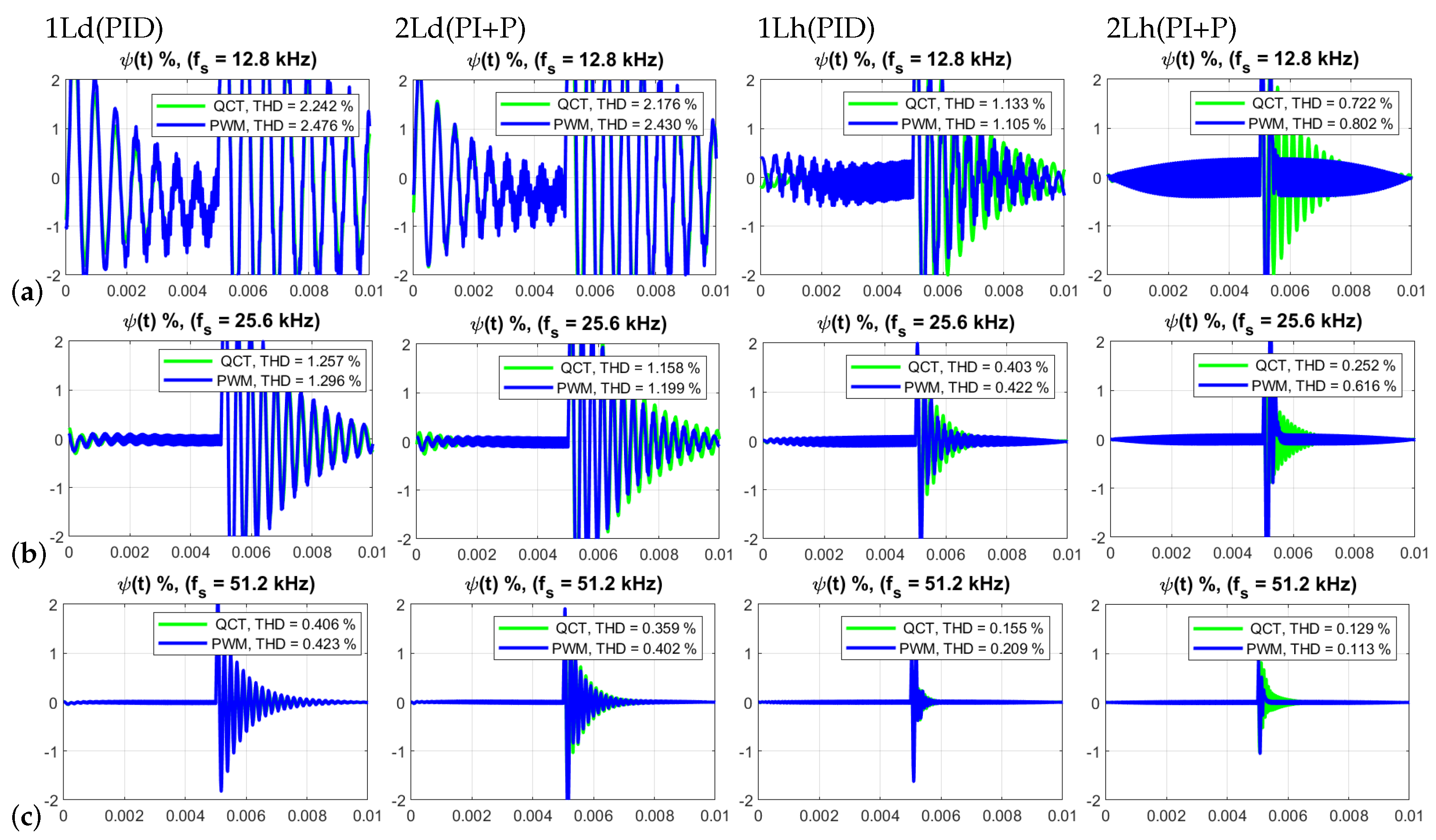
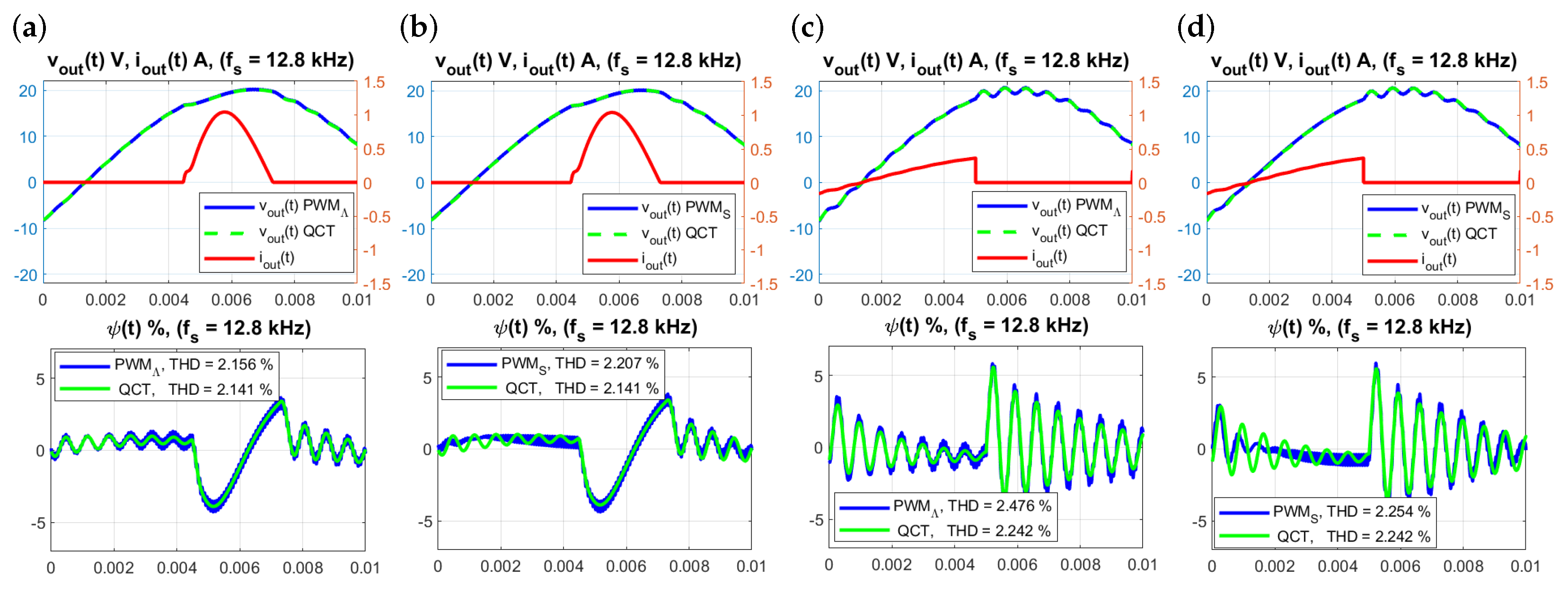
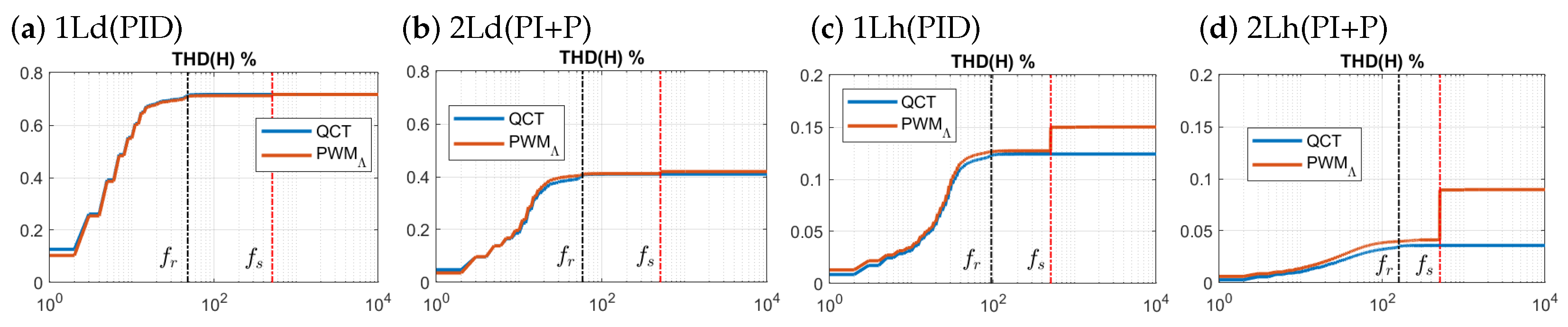
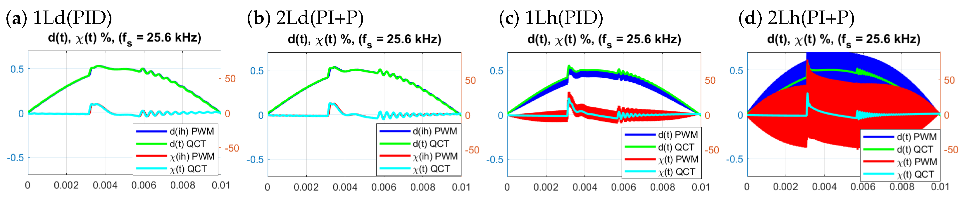
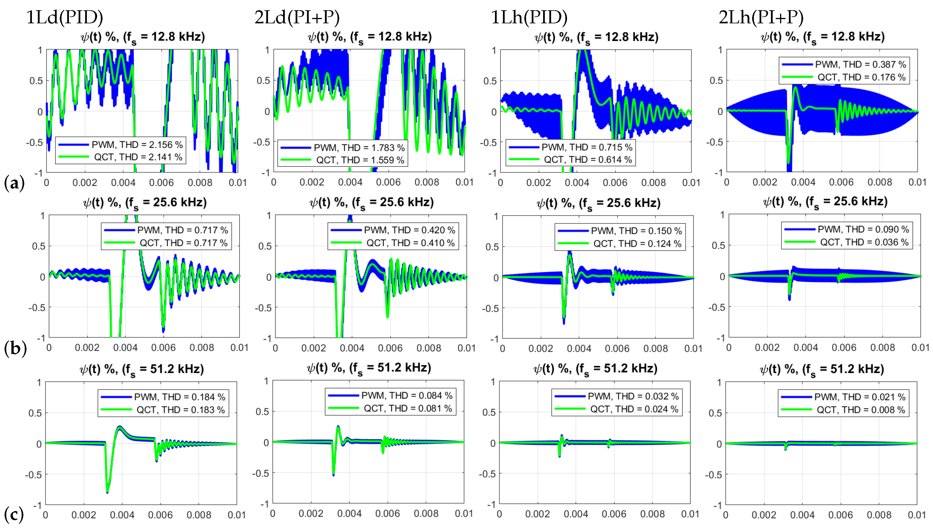
4.1. Results for the Basic Carrier Frequency kHz
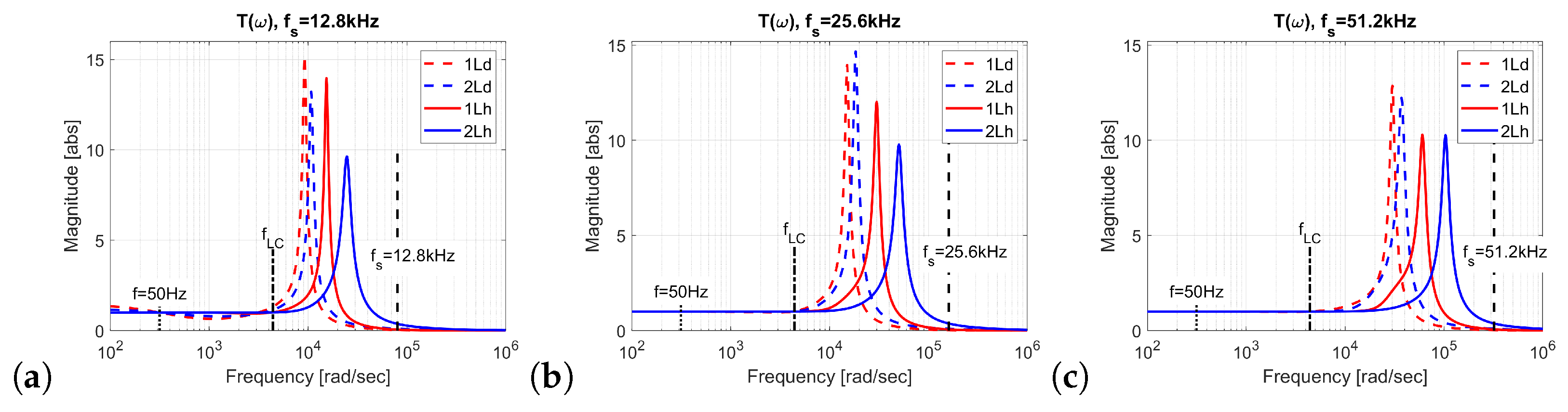
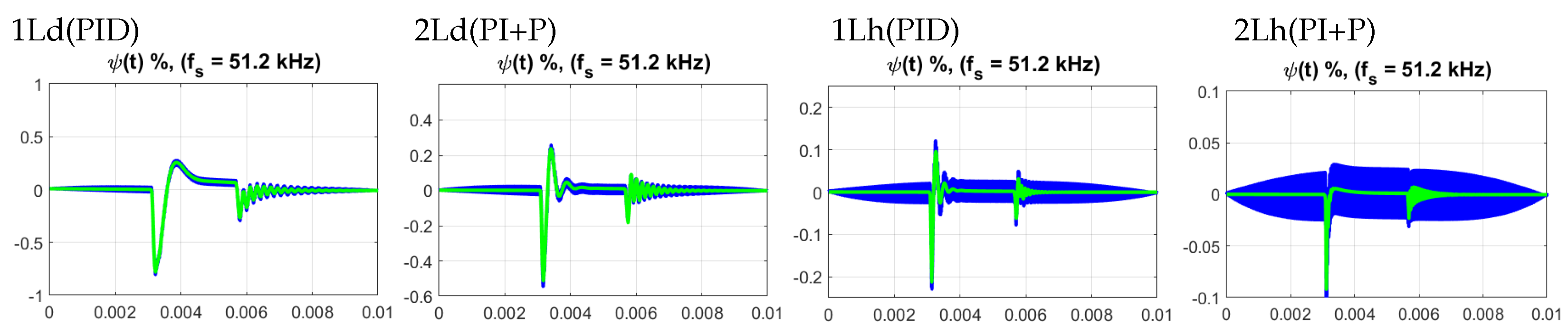
4.2. Results for Carrier Frequencies 12.8, 25.6 and 51.2 kHz
4.3. Abruptly Changing Resistive Load
5. Other Features
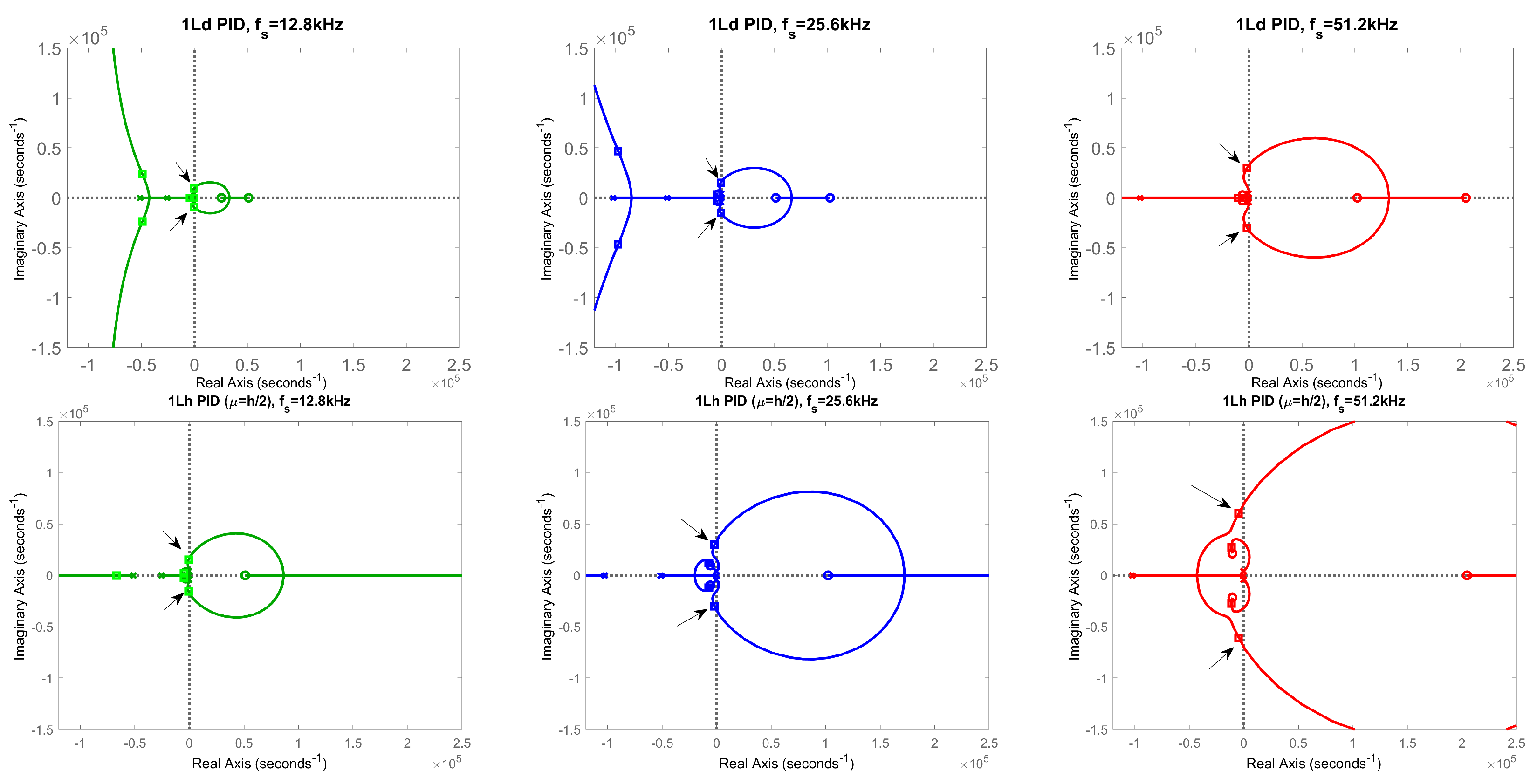
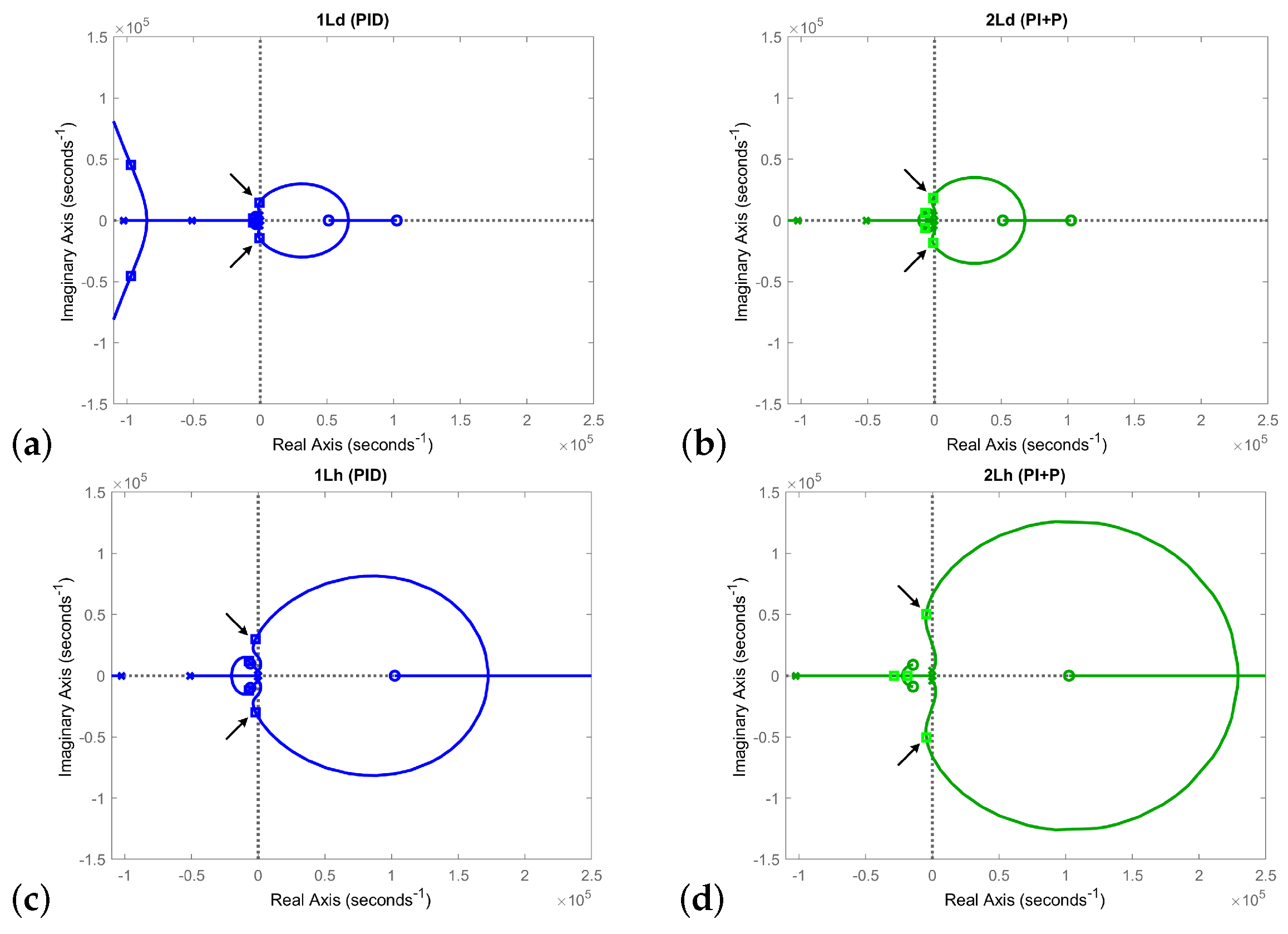
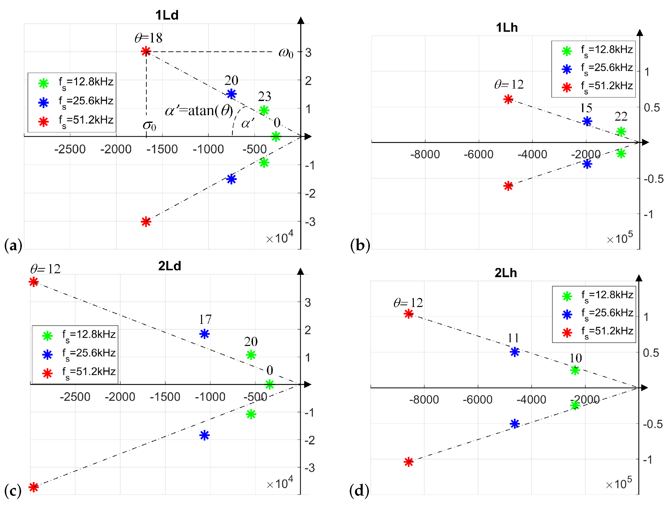
5.1. Closed-Loop Roots
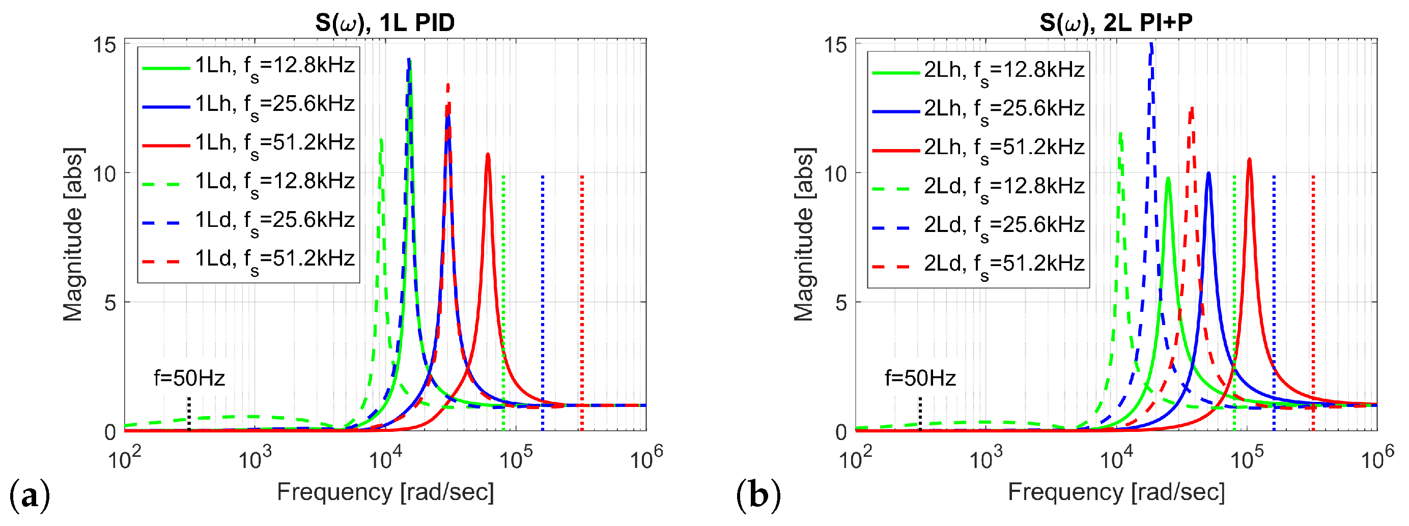
5.2. Closed-Loop Frequency Plots
5.3. Impact of PWM Type on Control
6. Comparison with Other Control Methods
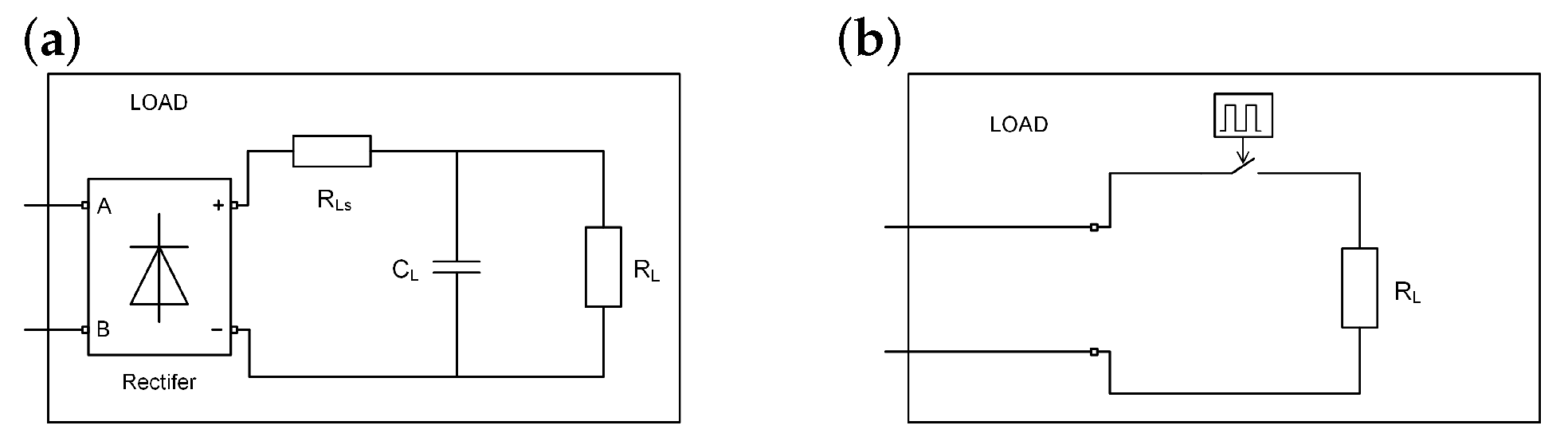
6.1. Open-Loop System with a Rectifier Load
6.2. Proportional Controller P
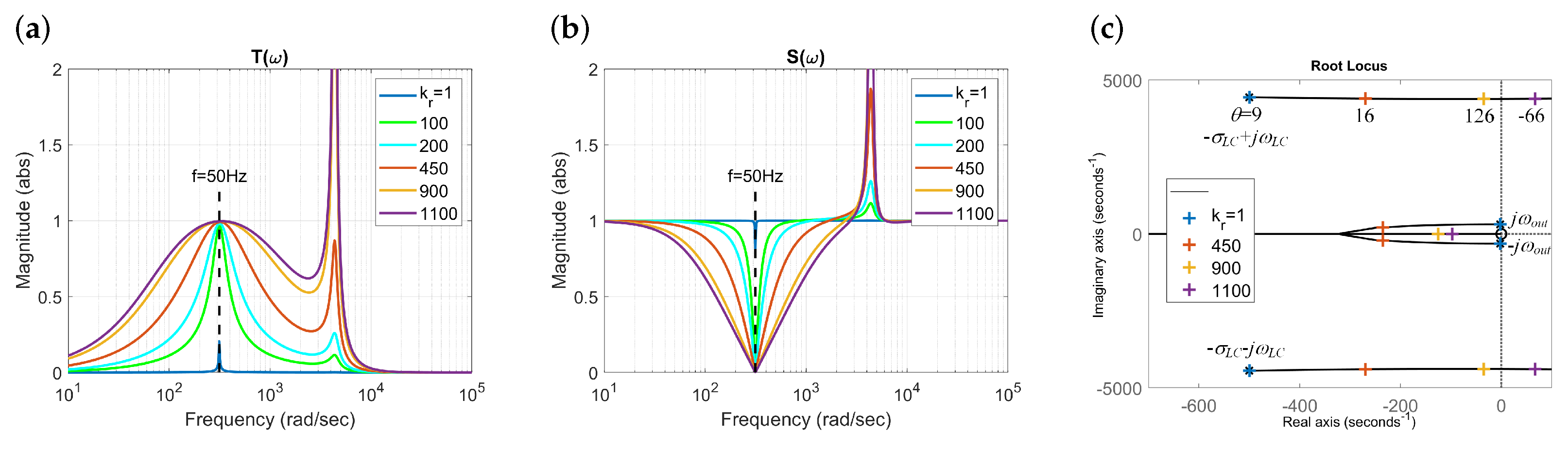
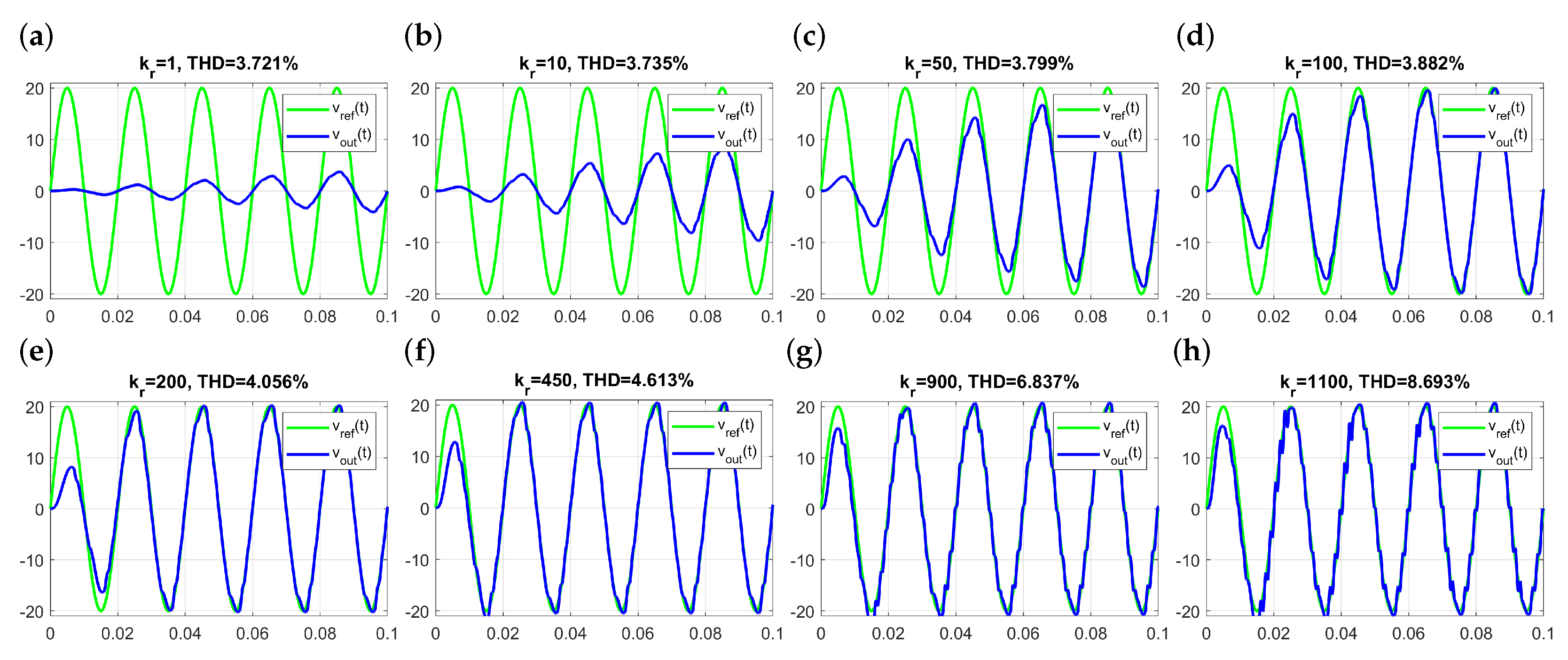
6.3. Resonant Controller R
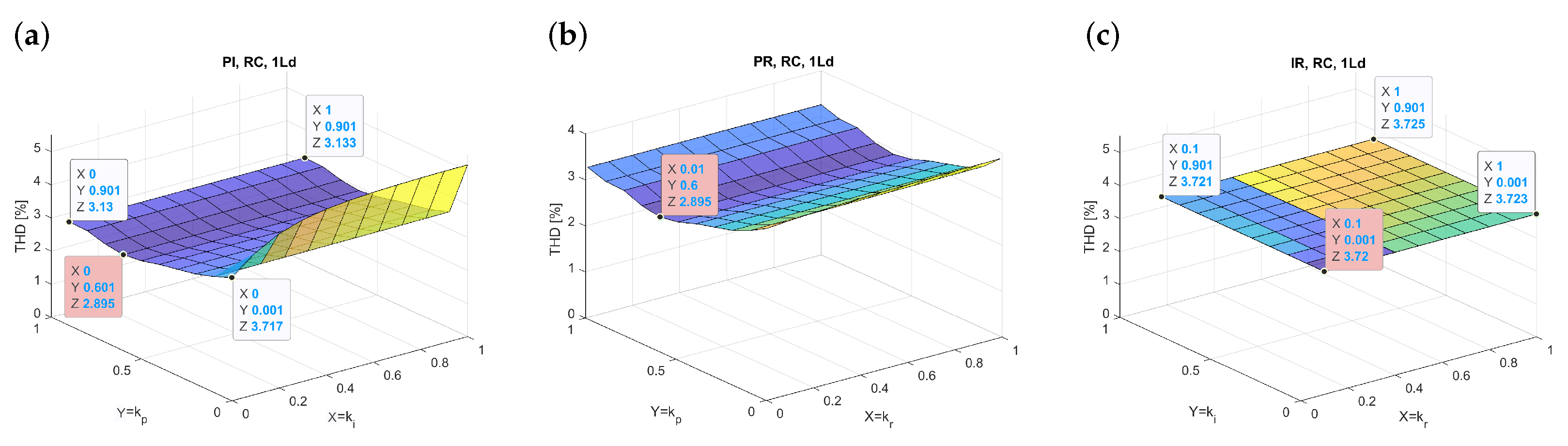
6.4. PI, PR, and IR Controllers
6.5. Summary
7. Conclusions
Author Contributions
Funding
Data Availability Statement
Conflicts of Interest
References
- Ortega, R.; Garcera, G.; Figueres, E.; Carranza, O.; Trujillo, C.L. Design and application of a two degrees of freedom control with a repetitive controller in a single-phase inverter. In Proceedings of the 2011 IEEE International Symposium on Industrial Electronics, Gdansk, Poland, 27–30 June 2011; pp. 1441–1446. [Google Scholar]
- Razi, R.; Karbasforooshan, M.-S.; Monfared, M. Multi-loop control of UPS inverter with a plug-in odd-harmonic repetitive controller. ISA Trans. 2017, 67, 496–506. [Google Scholar] [CrossRef] [PubMed]
- Rech, C.; Pinheiro, H.; Grundling, H.A.; Hey, H.L.; Pinheiro, J.R. Comparison of digital control techniques with repetitive integral action for low cost PWM inverters. IEEE Trans. Power Electron. 2003, 18, 401–410. [Google Scholar] [CrossRef]
- Zhang, K.; Kang, Y.; Xiong, J.; Chen, J. Direct repetitive control of SPWM inverter for UPS purpose. IEEE Trans. Power Electron. 2003, 18, 784–792. [Google Scholar] [CrossRef]
- Zhou, K.; Low, K.; Wang, D.; Luo, F.; Zhang, B.; Wang, Y. Zero-phase odd-harmonic repetitive controller for a single phase PWM inverter. IEEE Trans. Power Electron. 2006, 21, 193–201. [Google Scholar] [CrossRef]
- Mattavelli, P. An improved deadbeat control for UPS using disturbance observers. IEEE Trans. Ind. Electron. 2005, 52, 206–212. [Google Scholar] [CrossRef]
- Rymarski, Z.; KBernacki, K. Different Approaches to Modelling Single-phase Voltage Source Inverters for Uninterruptible Power Supply Systems. IET Power Electron. 2016, 9, 1513–1520. [Google Scholar] [CrossRef]
- Abrishamifar, A.; Ahmad, A.; Mohamadian, M. Fixed switching frequency sliding mode control for single-phase unipolar inverters. IEEE Trans. Power Electron. 2012, 27, 2507–2514. [Google Scholar] [CrossRef]
- Tai, T.L.; Chen, J.S. UPS inverter design using discrete time sliding mode control scheme. IEEE Trans. Ind. Electron. 2002, 49, 67–75. [Google Scholar]
- Bonan, G.; Mano, O.; Pereira, L.F.A.; Coutinho, D.F. Robust control design of multiple resonant controllers for sinusoidal tracking and harmonic rejection in Uninterruptible Power Supplies. In Proceedings of the IEEE International Symposium on Industrial Electronics, Bari, Italy, 4–7 July 2010; pp. 303–308. [Google Scholar]
- Khajehoddin, S.A.; Karimi-Ghartemani, M.; Jain, P.K.; Bakhshai, A. A resonant controller with high structural robustness for fixed-point digital implementations. IEEE Trans. Power Electron. 2012, 27, 3352–3362. [Google Scholar] [CrossRef]
- Parvez, M.; Elias, M.; Abd Rahim, N.; Blaabjerg, F.; Abbot, D.; Al-Sarawi, S. Comparative Study of Discrete PI and PR Controls for Single-Phase UPS Inverter. IEEE Access 2020, 6, 45584–45595. [Google Scholar] [CrossRef]
- Wang, X.; Loh, P.C.; Blaabjerg, F. Stability Analysis and Controller Synthesis for Single-Loop Voltage-Controlled VSIs. IEEE Trans. Power Electron. 2017, 32, 7394–7404. [Google Scholar] [CrossRef] [Green Version]
- Abdel-Rahim, N.; Quaicoe, J. Analysis and design of a multiple feedback loop control strategy for single-phase voltage source UPS inverter. IEEE Trans. Power Electron. 2003, 18, 1176–1185. [Google Scholar] [CrossRef]
- Woo, Y.T.; Kim, Y.C. Digital Control of a Single-Phase UPS Inverter for Robust AC-Voltage Tracking. Int. J. Control Autom. Syst. 2005, 3, 620–630. [Google Scholar]
- Wen, W.; Zhang, Y.; Zhan, T.; Jin, L.; Wang, L. A New Double Feedback Loop Control Strategy for Single-Phase Voltage-Source UPS Inverters. In Proceedings of the 2016 8th International Power Electronics and Motion Control Coference, (IPEMC-ESE Asia), Hefei, China, 22–26 May 2016. [Google Scholar]
- Ryan, M.; Brumsickle, W.; Lorenz, R. Control Technology Options for Single-Phase UPS Inverters. IEEE Trans. Ind. Appl. 1997, 33, 493–501. [Google Scholar] [CrossRef] [Green Version]
- Komurcugil, H. Improved passivity-based control method and its robustness analysis for single-phase uninterruptible power supply inverters. IET Power Electron. 2015, 8, 1558–1570. [Google Scholar] [CrossRef]
- Rymarski, Z.; Bernacki, K.; Dyga, Ł.; Davari, P. Passivity-Based Control Design Methodology for UPS Systems. Energies 2019, 12, 4301. [Google Scholar] [CrossRef] [Green Version]
- Serra, F.M.; De Angelo, C.H.; Forchetti, D.G. IDA-PBC control of a DC–AC converter for sinusoidal three-phase voltage generation. Int. J. Electron. 2017, 104, 93–110. [Google Scholar] [CrossRef]
- Monfared, M. A simplified control strategy for single-phase UPS inverters. Bull. Polish Acad. Sci. Tech. Sci. 2014, 62, 367–373. [Google Scholar] [CrossRef] [Green Version]
- Ryan, M.; Lorenz, R. A high performance sine wave inverter controller with capacitor current feedback and “back-EMF” decoupling. In Proceedings of the PESC ’95-Power Electronics Specialist Conference, Atlanta, GA, USA, 18–22 June 1995; Volume 1, pp. 507–513. [Google Scholar]
- Zaky, M. Design of Multiple Feedback Control Loops for a Single-phase Full-bridge Inverter Based on Stability Considerations. Electr. Power Compon. Syst. 2015, 43, 1–16. [Google Scholar] [CrossRef]
- Hamamci, S.E.; Kaya, I.; Koksal, M. Improving performance for a class of processes using coefficient diagram method. In Proceedings of the 9th Mediterranean Conference on Control and Automation, MED’01, Dubrovnik, Croatia, 27–29 June 2001; pp. 1–6. [Google Scholar]
- Manabe, S. Coefficient diagram method. In Proceedings of the 14th IFAC Symposium on Automatic Control in Aerospace 1998, Seoul, Korea, 24–28 August 1998; Volume 31, pp. 211–222. [Google Scholar]
- Van de Sype, D.; De Guesseme, K.; Van den Bossche, A.; Mekebeek, J. Small signal z-domain analysis of digitally controlled converters. In Proceedings of the 35th Annual IEEE Poser Electronics Specialists Conference, Aachen, Germany, 20–25 June 2004; pp. 4299–4305. [Google Scholar]
- Yepes, A.; Freijedo, F.; Doval-Gandoy, J.; Lopez, O.; Malvar, J.; Fernandes-Comesana, P. Effects of discretization methods on the performance of resonant controllers. IEEE Trans. Power Electron. 2010, 25, 1692–1712. [Google Scholar] [CrossRef]
- Blachuta, M.; Rymarski, Z.; Bieda, R.; Bernacki, K.; Grygiel, R. Continuous-Time Approach to Discrete-Time PID Control for UPS Inverters-A Case Study. In Proceedings of Intelligent Information and Database Systems, ACIIDS 2020; Lecture Notes in Computer Science; Springer: Cham, Switzerland, 2020; Volume 12033. [Google Scholar]
- Rymarski, Z.; Bernacki, K. Different Features of Control Systems for Single-Phase Voltage Source Inverters. Energies 2020, 13, 4100. [Google Scholar] [CrossRef]
- Rymarski, Z.; Bernacki, K. Technical Limits of Passivity-Based Control Gains for a Single-Phase Voltage Source Inverter. Energies 2021, 14, 4560. [Google Scholar] [CrossRef]
- Blachuta, M.; Bieda, R.; Grygiel, R. Sampling Rate and Performance of DC/AC Inverters with Digital PID Control—A Case Study. Energies 2021, 14, 5170. [Google Scholar] [CrossRef]
- Bowes, S.R.; Holliday, D.; Grewal, S. Comparison of single-phase three-level pulse width modulation strategies. Electric Power Appl. IEE Proc. 2004, 151, 205–214. [Google Scholar] [CrossRef]
- Koseoglu, C.; Altin, N.; Zengin, F.; Kelebek, H.; Sefa, I. A hybrid overload current limiting and short circuit protection scheme: A case study on UPS inverter. In Proceedings of the 8th International Conference on Renewable Energy Research and Applications, ICRERA 2019, Brasov, Romania, 3–6 November 2019; pp. 957–962. [Google Scholar]
- Lu, B.; Sharma, S.K. A literature review of IGBT fault diagnostic and protection methods for power inverters. IEEE Trans. Ind. Appl. 2009, 45, 1770–1777. [Google Scholar]
- Corradini, L.; Maksimović, D.; Mattavelli, P.; Zane, R. Digital Control of High-Frequency Switched-Mode Power Converters; John Wiley & Sons, Inc.: Hoboken, NJ, USA, 2015. [Google Scholar]
- Maksimović, D.; Zane, R.; Erickson, R. Impact of digital control in power electronics. In Proceedings of the 16th International Symposium on Power Semiconductor Devices and ICs, Kitakyushu, Japan, 24–27 May 2004. [Google Scholar]
- Patella, B.J.; Prodić, A.; Zirger, A.; Maksimović, D. High-frequency digital PWM controller IC for DC-DC converters. IEEE Trans. Power Electron. 2003, 18, 438–446. [Google Scholar] [CrossRef] [Green Version]


| M | (kHz) | PAM | PWM | PWM | PWM |
|---|---|---|---|---|---|
| 12.8 | 0.5000 | 0.0849 | 0.5000 | 0.5000 | |
| 0.2 | 25.6 | 0.5000 | 0.0849 | 0.5000 | 0.5000 |
| 51.2 | 0.5000 | 0.0849 | 0.5000 | 0.5000 | |
| 12.8 | 0.5000 | 0.2122 | 0.5000 | 0.5000 | |
| 0.5 | 25.6 | 0.5000 | 0.2122 | 0.5000 | 0.5000 |
| 51.2 | 0.5000 | 0.2122 | 0.5000 | 0.5000 | |
| 12.8 | 0.5000 | 0.3395 | 0.5000 | 0.5000 | |
| 0.8 | 25.6 | 0.5000 | 0.3395 | 0.5000 | 0.5000 |
| 51.2 | 0.5000 | 0.3395 | 0.5000 | 0.5000 |
| PWM and PWM | PWM | |||||
|---|---|---|---|---|---|---|
| (kHz) | 0.2 | 0.5 | 0.8 | 0.2 | 0.5 | 0.8 |
| 12.8 | 0.4263 | 0.3201 | 0.1913 | 0.4479 | 0.4693 | 0.5814 |
| 25.6 | 0.1063 | 0.0798 | 0.0477 | 0.1266 | 0.1892 | 0.2786 |
| 51.2 | 0.0266 | 0.0199 | 0.0119 | 0.0435 | 0.0881 | 0.1378 |
| (kHz) | 1L (PD) | 2L (P+P) | 1L (PID) | 2L (PI+P) |
|---|---|---|---|---|
| digital | ||||
| 12.8 | = 8.5 | = 8.4, = 0.20 | = 9.1 | = 8.1, = 0.22 |
| 25.6 | = 31.7 | = 15.5, = 0.50 | = 35.9 | = 17.2, = 0.45 |
| 51.2 | = 124.6 | = 30.4, = 1.01 | = 146.9 | = 37.2, = 0.80 |
| hybrid | ||||
| 12.8 | = 19.1 | = 23.3, = 0.78 | = 20.3 | = 23.3, = 0.72 |
| 25.6 | = 73.8 | = 46.5, = 1.55 | = 90.1 | = 46.5, = 1.45 |
| 51.2 | = 294.9 | = 93.1, = 3.08 | = 379.1 | = 93.1, = 2.95 |
| (kHz) | 1L (PD) | 2L (P+P) | 1L (PID) | 2L (PI+P) |
|---|---|---|---|---|
| digital: | ||||
| 12.8 | 2.011/1.980 | 1.753/1.469 | 2.156/2.141 | 1.782/1.559 |
| 25.6 | 0.793/0.786 | 0.548/0.506 | 0.717/0.717 | 0.419/0.409 |
| 51.2 | 0.239/0.238 | 0.150/0.144 | 0.184/0.183 | 0.083/0.081 |
| hybrid: | ||||
| 12.8 | 0.848/0.672 | 0.534/0.242 | 0.715/0.614 | 0.387/0.176 |
| 25.6 | 0.241/0.202 | 0.121/0.064 | 0.150/0.124 | 0.089/0.036 |
| 51.2 | 0.063/0.054 | 0.028/0.016 | 0.032/0.024 | 0.021/0.007 |
| (kHz) | 1Ld (PID) | 2Ld (PI+P) | 1Lh (PID) | 2Lh (PI+P) |
|---|---|---|---|---|
| (Hz) | ||||
| 12.8 | 1470 | 1714 | 2447 | 3929 |
| 25.6 | 2396 | 2930 | 4770 | 8018 |
| 51.2 | 4798 | 5938 | 9650 | 16,533 |
| and | ||||
| 12.8 | n.a. | n.a. | ||
| ) | ||||
| 25.6 | ||||
| 51.2 | ) | |||
| (kHz) | 1Ld (PID) | 2Ld (PI+P) | 1Lh (PID) | 2Lh (PI+P) |
|---|---|---|---|---|
| (Hz) | ||||
| 12.8 | 1479 | 1714 | 2446 | 3930 |
| 25.6 | 2395 | 2927 | 4770 | 8013 |
| 51.2 | 4795 | 5922 | 9650 | 16,520 |
Publisher’s Note: MDPI stays neutral with regard to jurisdictional claims in published maps and institutional affiliations. |
© 2022 by the authors. Licensee MDPI, Basel, Switzerland. This article is an open access article distributed under the terms and conditions of the Creative Commons Attribution (CC BY) license (https://creativecommons.org/licenses/by/4.0/).
Share and Cite
Blachuta, M.; Bieda, R.; Grygiel, R. High Performance Single and Double Loop Digital and Hybrid PID-Type Control for DC/AC Voltage Source Inverters. Energies 2022, 15, 785. https://doi.org/10.3390/en15030785
Blachuta M, Bieda R, Grygiel R. High Performance Single and Double Loop Digital and Hybrid PID-Type Control for DC/AC Voltage Source Inverters. Energies. 2022; 15(3):785. https://doi.org/10.3390/en15030785
Chicago/Turabian StyleBlachuta, Marian, Robert Bieda, and Rafal Grygiel. 2022. "High Performance Single and Double Loop Digital and Hybrid PID-Type Control for DC/AC Voltage Source Inverters" Energies 15, no. 3: 785. https://doi.org/10.3390/en15030785
APA StyleBlachuta, M., Bieda, R., & Grygiel, R. (2022). High Performance Single and Double Loop Digital and Hybrid PID-Type Control for DC/AC Voltage Source Inverters. Energies, 15(3), 785. https://doi.org/10.3390/en15030785