1. Introduction
Semiconductor superlattices (SL) are nanostructures whose properties were discovered in the 1970s [
1], still the first real devices were produced twenty years later [
2]. Currently, they are used for building quantum cascade lasers [
3,
4] which are used in several important industry sectors [
5]. Due to the high complexity of the physical processes occurring in the SL structures, their computer simulations require either high computing power, or highly effective computational methods. Therefore, over the recent years, many numerical models have been developed for SL structures. In the simplest one [
5,
6,
7,
8] a constant potential and the effective mass of electrons in each layer of the structure are assumed. A popular approach to solving the Schrödinger equation in cascade struktures is provided by the rate equation method (RE) [
9,
10,
11,
12] where the boundary conditions in the form of hard walls at the edges of the structure composed of three consecutive periods of SL are assumed, and the solutions obtained for the central period are considered to be representative for the whole system. The Monte Carlo method (ME) [
13,
14,
15], based on solving the Boltzman equation, is another approach. Non-equilibrium Green’s function formalism (NEGF) [
16,
17] however, is the approach that offers the most versatile opportunities for simulating superlattices. This approach relies on self-consistent solving of Dyson, Keldysh and selfenergy equations either in the real space (real space method—RSM) [
18,
19,
20], or by means of the Wannier functions (Wannier function method—WFM) [
21,
22]. Under WFM infinite geometrical dimensions of the superlattice, and periodic delocalised Bloch functions over the whole structure are considered. To provide an alternative to such approaches we have built a finite model of the superlattice (FMSL) [
23], where the base of the wave functions that is the solution to the Schrödinger equation for the SL model of finite geometrical dimensions is applied. Despite many studies on the semiconductor superlattices properties, conducted both from the empirical and theoretical perspective, many factors that influence the transport parameters of the devices based on such structures still remain unexplored. We believe them to be the ground for the observed discrepancies between the simulation results and measurements performed on real devices. Thus, the pressure to find new tools for studying SL properties under different conditions and fields is still considerable. The influence of finite geometrical sizes on the quantum phenomena occurring in these structures is one of many issues to be studied. Our FMSL [
24] where the base of wave functions being the solution to the Schrödinger equation for the superlattice model with a finite geometry is applied, provides quite a suitable tool for such studies.
This paper presents new elements of the FMSL that allows quick studies on the influence of an unbalanced charge, and the voltage applied, on the tested device transport parameters, to be performed. Polynomials used to approximate the charge and potential distribution functions in a SL allow to obtain semi-analytical solutions for the Schrödinger and Poisson equations, where the variable potential in a single structure layer is taken into account without the necessity of dividing it into many sub-areas once the voltage to the system is applied. The presented method is effective in finding eigenstates extended over relatively large superlattice areas. The obtained quantum states are very similar to the Wannier-Stark functions and they can form the basis for the NEGF formalism. In order to confirm such a thesis, exemplary results for Schrödinger and Poisson solutions for superlattices based on GaAs/AlGaAs heterostructure are presented.
2. Formulation of the Problem
In most cases SL are simply stratified unipolar, n-type nanodevices [
25].
Figure 1. shows an example of the AlGaAs-GaAs device presented in [
26].
Hence, the electrons are subject to the quantum laws, i.e., under the Schrödinger equation with 1D Hamiltonian in the growth
d(
z) direction within the plane kinetic energy term
, where
is the magnitude of the in-plane momentum
k. In total, it can be written as
where
Ψ(
z) are envelope functions,
me(z) is the effective mass constant within each semiconductor layer, whereas
V(
z) is a spatially dependent total potential energy which can be written as
where
VSL(
z) represents the superlattice potential,
VB(
z) is the potential from the applied voltage, and
VS(
z) denotes the potential derived from impurities and unbalanced charge carriers.
The numerical model of SL presented so far [
23,
24] have some problems. It consists in the necessity to divide the superlattice layers into many sub-areas with a constant potential (see
Figure 2A). In the case of an applied voltage this significantly increases the Hamiltonian device matrix in size. The previous model also does not allow for the consideration of an unbalanced charge. In the present work we propose a solution to these problems by using a polynomial approximation of the potential (see
Figure 2B) and then to the charge distribution in the whole SL structure.
Many previous calculations (e.g., [
27,
28]) have shown, that in SL the conduction band is divided into minibands. With the wave functions in the above-mentioned minibands known, it is possible to determine the electron charge distribution within the SL as
where
ni describes the electrons concentration in the miniband
i according to
The total charge distribution can be written as
where
ND is the donor dopant concentration. The charge
ρ(z) generates a potential consistent with the Poisson equation
where
ε is dielectric function. On the border of each layer of the structure, the potential must meet the continuity conditions
where
zj represents the coordinate of the beginning of the
j-th SL layer (see
Figure 1), while
V is the function of the potential within this layer. The same conditions are fulfilled by the wave function
In addition, the boundary conditions at the beginning and the end of the structure need to be considered. In our model (see
Figure 1) they correspond to the source and the drain, respectively. For the potential function such conditions result from the applied voltage
U and it can be written as
For the wave function, the conditions correspond to the amplitudes of waves coming from the source and drain, and generally it can be formulated differently [
26]. All in all, the problem is to determine three coupled fields
V,
Ψ, and
ρ, described by Equations (1)–(6), under boundary conditions (7)–(11).
3. The Main Algorithm of Calculations
The solution of the problem formulated in the previous section requires the fields V, Ψ, ρ, to be self-consistent, which is achievable by calculations with an iterative algorithm applied. The first step is to find the energies and eigenfunctions of the Equation (1) for the VSL and the VB potentials. For VB = 0, the solution of the Equation (1) can be presented as a linear combination of elementary functions, namely plane waves running opposite each other. The standard TMF method is convenient for determining their amplitudes. Incorporating in the next iteration steps the potential of VB, as well as the potential of VS, the solutions to Equation (1) are no longer possible to be presented as elementary functions. Hence, we propose to use solution to the Equation (1) in the form of power series. Such a representation can be obtained analytically, for the potential expressed as a polynomial, or generally, as a power series. By Equation (6) the charge density function takes an analogous form. Therefore, it is suggested to approximate the charge density function with a polynomial, separately for each of the layers, at each step of the calculation procedure, following the solution of Equation (1) and by applying (3)–(5).
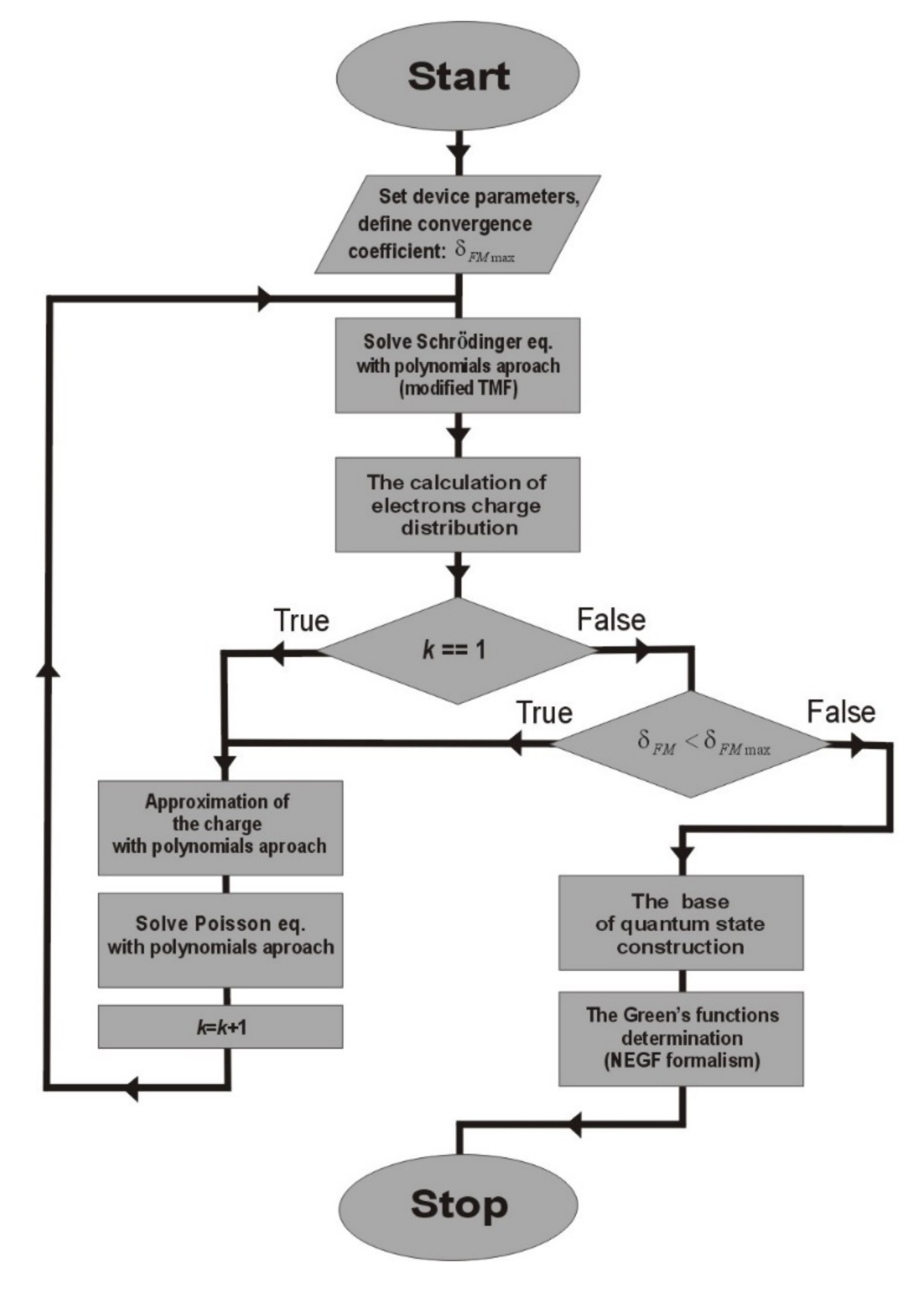
The main algorithm of the method under consideration is shown in
Figure 3.
One of the basic input parameters is the convergence coefficient defined as
where
ρk represents the electron charge density for the
kth iteration. The algorithm runs a loop for
δ >
δFM max. The next programmed operation involves applying the computed wave functions for constructing the quantum states base, to be used in NEGF procedures.
It is worth noting that the self-consistent method for solving the Poisson and Schrödinger equations with the presented algorithm is less complex than the algorithm presented earlier [
29], where repeated running of the NEGF blocks have been required that engaged most of the computing power.
The algorithm proposed under the paper significantly speeds up the simulation process and provides an important element of an effective SL model. A detailed description of each of its elements is provided in the following sections.
6. NEGF Modelling of Superlattice Structure
The FMSL under the paper incorporated the NEGF formalism into calculating transport parameters. As a part of the NEGF procedure, the Dyson and Keldysh equations are solved to determine the retarted Green’s (
GR) and correlation (
G<) functions, respectively. the model described here has an implemented procedure for calculating Green’s function based on the WFM method [
29] where we solve Dyson equation in the form
where
H is the Hamiltonian of the device,
is the matrix of the retarded Green’s functions and
ΣR is the matrix of self energies. The Keldysh equation takes the form
where
is the matrix of non-equilibrium Green functions, also called density or correlation functions. The elements of the self energy matrices (
Σ< and
ΣR) are found in the procedure of solving self-consistent solution equations together with the matrix elements
G< and
GR, respectively for the considered electron scattering mechanisms. This allows to determine transport parameters of the tested device, such as the density of state (DOS) [
23].
and electron density
Transport parameters under this study were calculated with a module into which the Büttiker probes had been implemented [
25]. It is a well known approach to solving Equations (49) and (50), the essence of which is the exchange of electrons between each quantum state of the active device and the virtual electrode attached to it (a Büttiker probe) containing the electron reservoir. As the result, self-consistent Fermi levels for the quantum and electrochemical state of the electrode are attained. It allows to determine the occupation of states in a wide energy range. It is also worth noting that such a method for determining Green’s function is very effective, as shown in our earlier paper [
28].
Under another research [
29], we found that the calculation speed can be significantly reduced when the approach with the WFM method is applied, according to which the Hamiltonian matrix is written as a sum,
with the matrix
representing the sum of states for the non-polarized (
) and polarized (
) superlattice, and the matrix
containing all electron scattering effects. Detailed definitions of all of the above Hamiltonian matrices are given in our previous papers [
29,
30] whereas this article has been focused on one of them only, related to the applied voltage, which appears in the form
where
e is the electron charge,
ξ is the electric field,
n stands for the number of the considered superlattice period of length—
d,
k is the wave vector, and the parameters
and
are state operators, namely creation and annihilation of the ν state, respectively. The variable
included in the definition (51) calculated as
is called overlapping states integral. The interaction between the minibands (indices
μ, ν) and the superlattice periods (index
l) are taken into account by this relation. Under IMS model [
28] the W (z) functions correspond to the Wannier and Wannier-Stark basis for unpolarised and polarised superlattice structures, respectively, whereas under the FMS model they correspond to the constructed quantum states described elsewhere [
23]. Under this paper, we use the base of eigenstates that was created by solving the Schrödinger equation on the basis of the procedure presented elsewhere [
23].
7. Simulations Results
The correctness and effectiveness of the developed numerical method has been checked by simulating typical superlattice structures whose parameters are widely available elsewhere [
26,
28] that for the purpose of this paper are called structure 1 and structure 2, respectively. They are presented in
Table 1.
An important part of numerical research was concerned with assessing the impact of the SL geometrical sizes on the quantum states properties. The results of the research in this area are illustrated in
Figure 4. The energy eigenvalues distributions calculated with the FMSL are clearly dependent on the number of the superlattice periods considered. Picture (A) presents the results for a simple symmetrical superlattice that consists of one well and one barrier in the period (structure 1), while picture (B) displays the eigenvalues of energy for a typical terahertz laser structure (structure 2). The results show a general tendency for the energy eigenvalues to group within the minibands. The minibands boundaries are defined by the number of SL periods. This is very clearly seen in the graphs presented in
Figure 4A, thought it is less clearly pronounced in
Figure 4B, due to the very narrow minibands for this SL.
It is also worth noting that the eigenstates located near the upper edge of the minibands exceed the energy barrier levels (ΔEC) already for 4 periods for structure 1, and 8 periods for structure 2. When these states are occupied by electrons, it may have a significant impact on transport.
In
Figure 4. it can also be observed that the greater number of the periods considered in the calculations, the more precisely the minibands edges are determined. It indicates the necessity of considering the greatest possible number of SL periods in simulations. Regretfully, it practically brings very high load to calculating machines, as well as decreases simulations efficiency.
Therefore, a question arises on the SL periods number to be taken into account in simulations that would give the exact results for the miniband distribution, without the efficiency loss for calculating SL parameters. A comparison of the presented results with the results obtained by means of IMSL may provide an answer. To compare we used the coefficient defined as
where
—is the value of the parameter for the
υ - miniband calculated using the IMSL, while
it is the value of the same parameter determined by using of the FMSL.
From important parameters that characterize superlattices the minibands width (ΔE) and the location of the miniband centers energy (E
center) were selected to compare both models. Then the values were determined for each miniband of the considered structure, and their dependence on the number of SL periods with the FSML model, and compared to the results obtained with IMSL. The results are illustrated in
Figure 5. Both models were found to converge nicely for simulations with 40 SL periods taken into account under FMSL. The differences increased to less than 1%, and to 0.1% for the width of the minibands (ΔE) and the position of their centers (E
center), respectively. It was observed for both simulated structures. It is worth noting here that the obtained results are also consistent with the results published in [
29]. In addition practical implementations for structure 1 contain several hundred periods, whereas for structure 2 the number of periods to be considered is equal to 190 [
26]. Hence, any errors due to assumed infinite sizes in IMSL seem negligible.
On the other hand, it can be also argued that slight differences observed in the results are encouraging with regards to applying the FMSL to a greater extent than it has been practiced so far. It is clear that the developed method allows to engage the structure bias voltage directly in the process of solving the Schrödinger and Poisson equations. The calculations showing the results are presented in
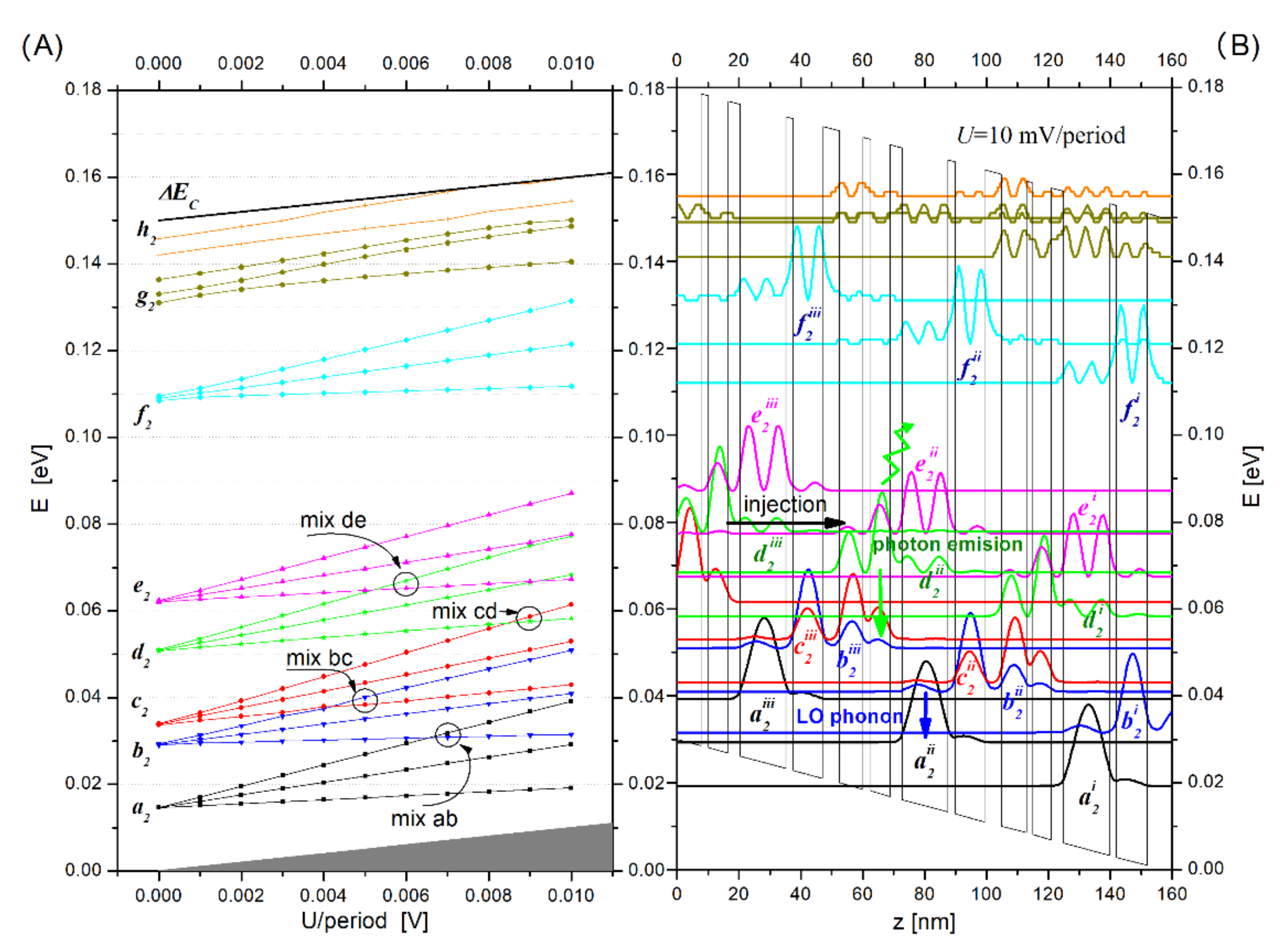
Figure 6A shows the bias voltage influence on the eigenenergy distribution for the structure 2, calculated by means of the FMSL. The effect of so-called mixing eigenstates from different minibands can be observed. For example, from the voltage of 5 mV/period, the energy for the highest state of miniband
b2 is greater than the lowest state of miniband
c2 (mix bc). From the voltage of 6 mV/period, it can be seen that the highest state of the
d2 miniband occupies a higher energy level than the lowest state of the
e2 miniband (mix de). For another case, the energy of the highest state of miniband
a2 is greater than for the lowest state of miniband
b2 (mix ab) already from the voltage of 7 mV/period, and from the voltage of 9 mV/period, the energy for the highest state of miniband
c2 is greater than the lowest level of miniband
d2 (mix ab). All the cases can result in the interband transitions combined with tunneling effects through the potential barriers. These are the electronic transport features characteristic for this type of SL structures.
Potential occurrences of such quantum effects are illustrated with
Figure 6B, where we can see the wave functions (modules squared) for the bias voltage of 10 mV/period applied to the structure.
Mixed quantum states with similar eigenvalues, for example and , drawn in green and pink, respectively, located in adjacent quantum wells separated by narrow potential barriers are found there. It enables the electron tunnel transport in the local area of the superlattice, even as far as to the next period, to the energy level from the higher mini-band. This is a process known as charge carrier injection. In the next stage, electrons from a higher energy level due to local inversion of occupations can be subject to a coherent transition to the average level (for example ) emitting a photon with an energy characteristic for the simulated structure (here 14 meV). Vertical transitions incoherent between quantum states emitting LO phonons with the energy of 37.5 meV, such as transitions , are also possible, with appropriately biased voltage. Such processes result in a electron cascade flux transporting the charge along the superlattice structure, and they provide the basis for cascade lasers operation. However, the precise conditions for such transport can be established only following the NEGF formalism.
In order to perform such calculations, a base of quantum states adequate to the current bias voltage should be constructed and applied to creating the tested device Hamiltonian matrix (51), which comprises the input data of the program block calculating Green’s functions. Calculations results for several various quantum states bases are known [
31,
32] and they can serve as the bases for positional quantum states, the quantum states Wannier functions, or the Wannier - Stark functions. So far all the models developed by our team have applied the Wannier and Wannier-Stark base for the IMSL [
29], and the base of quantum states defined for the FMSL [
23]. The disadvantage of the latter is that the quantum states representing individual minibands are not localized within one SL period. It implies the necessity of including at least five structure periods in the tested device Hamiltonian matrix, while in the IMSL only three structure periods are required for the same purpose. In the approach under the paper, all the obtained quantum states are very well localized within a single SL period, as is the case with the base of quantum states of the IMSL. Hence, the size of the Hamiltonian matrix can be limited to 3 SL periods, as in the IMSL.
With the quantum states base shown in
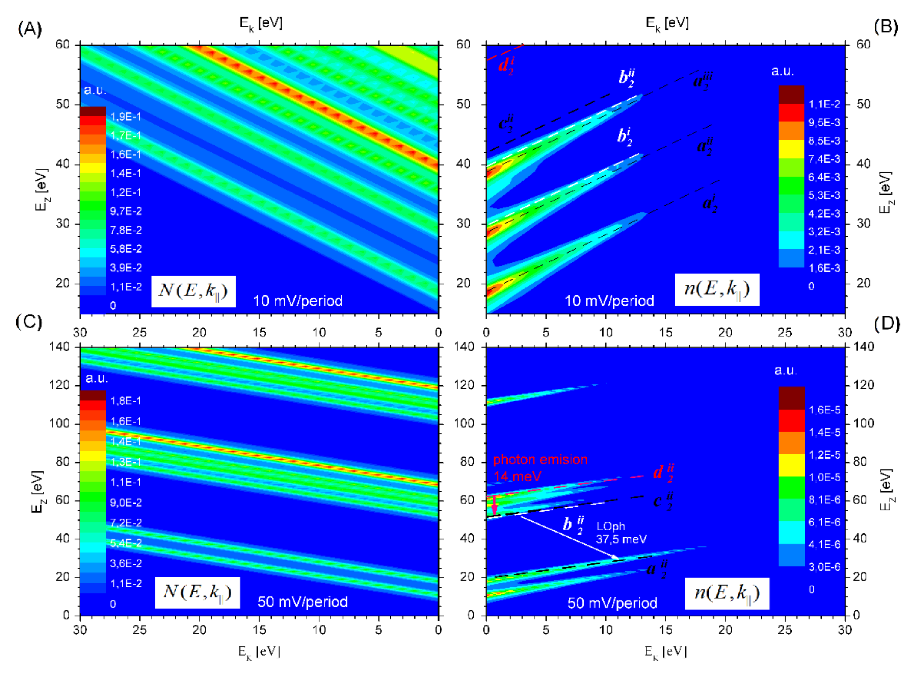
Figure 6 and the size of the Hamiltonian matrix limited to three SL periods, the transport parameters for structure 2 are simulated and selected examples of the results are shown in
Figure 7.
Maps of DOS (
) and occupation by electrons (
) functions in the energy space of the wave vector k are also presented. The calculations run at the assumed temperature
T = 77 K. The graphs (A) and (B) were made for the bias voltage of
U = 10 mV/period, while the graphs (C) and (D) are related to the voltage
U = 50 mV/period. By analyzing the results, it can be concluded that for a small voltage applied to the structure (10 mV/period) we observe a high density of states in the energy range corresponding to their eigen energies (see
Figure 6B). Electrons occupy only the lowest states (
and
) and there is no visible inversion of occupations opening the possibility for photons emission (transitions
), or phonons (transitions
). The situation is different for the superlattice biased with voltage of 50 mV/period (see
Figure 7D). The higher energy states (e.g.,
) show then a greater occupation than the mid-states (
), so electronic transitions emitting photons with an energy of 14 meV may occur. Additionally, transitions in the
k-vector space emitting optical phonons with an energy of 37.5 meV are also likely to occur. More detailed research with NEGF applied in this area was published earlier [
23,
29].
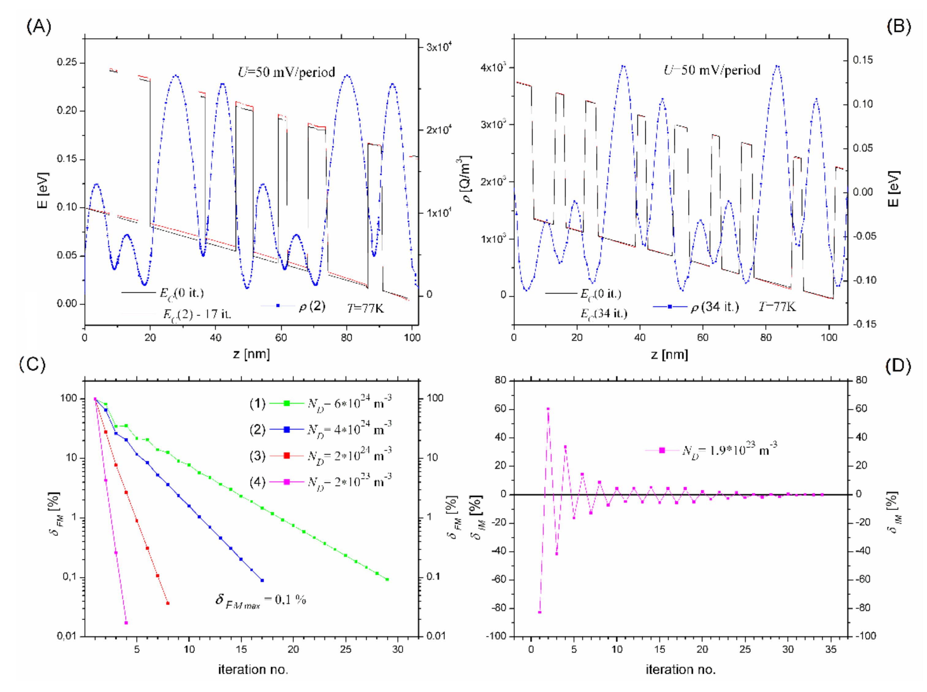
This article has been aimed at testing the correctness of a newly developed computational module, whose main task is to effectively find self-consistent potential and charge in a biased voltage SL structure. For this purpose, simulations for typical SL structures were carried out, the results of which are presented in
Figure 8A shows the results of a self-consistent solution for the Schrödinger and Poisson equations with regards to potential and total charge distributions in the structure 2 with a bias voltage at 50 mV/period; the structure has been doped at
ND = 4 × 10
24 m
−3. Graph (C) shows convergence of the method for different doping levels, i.e.,
δFM coefficient (see Equation (12)) versus the iteration number dependencies.
The convergence of the method was tested in a relatively wide range of impurity concentrations, namely from
ND = 2 × 10
23 m
−3 to
ND = 6 × 10
24 m
−3. The results prove the method to be quickly convergent and to require a maximum of 30 iterations, with the minimum charge change of
δ FMmax < 0.1% assumed. Simulations for the same structure with the input parameter defined with the Newton-Rapson method [
33] were performed for comparison purposes. The results are represented by charts (B) and (D). Chart (B) presents the potential energy
EC distributions and the total charge
ρ(
z) for the polarized structure, doped at the level of
ND = 1.9 × 10
23 m
−3, while graph (D) displays the dependence between
δIM coefficient and the number of iterations. The convergence coefficient
δIM is calculated from
where
k is the iteration number,
stands for the input parameter assumed at 10
−4 V, and
denotes the potential correction calculated according to the procedure presented in [
33].
By analyzing the results shown in
Figure 8A in relation to the graphs presented in
Figure 8B correctness of the new method can be considered confirmed, as similar results with regards to both total charge density distribution and its influence on the
EC potential were obtained. With regards to the results shown in graphs (C) it should be noted that the very high doping
ND = 6 × 10
24 m
−3 has not prevented us from achieving good convergence. However, it is not the case for the Newton-Rapson method. As seen from chart (D) a relatively low level of doping, namely
ND = 1.9 × 10
23 m
−3, requires 34 iterations for the charge and potential within the structure to be elf-consistent under the conditions specified in
Figure 8, and for very high doping levels convergence problems may occur. Similar cases have been reported [
34] and PID blocks were recommended for the method algorithm in order to obtain stable and self-balanced procedure for the charge and potential, which in turn is associated with a significant extension of the simulation time.
The linear relationships on
Figure 8C suggest that the convergence of the developed method is exponential (ordinate axis is on a logarithmic scale). This is its great advantage, because it means fast convergence as well as allows to predict simulation time.


