Article

Commutation Behavior and Stray Inductance Analysis of a FC-3L-BDC Phase-Leg PEBB

1
School of Traffic & Transportation Engineering, Central South University, Changsha 410083, China
2
CRRC Zhuzhou Institute CO., Ltd., Zhuzhou 412001, China
*
Author to whom correspondence should be addressed.
Energies 2022, 15(24), 9651; https://doi.org/10.3390/en15249651
Submission received: 25 October 2022 / Revised: 6 December 2022 / Accepted: 15 December 2022 / Published: 19 December 2022
(This article belongs to the Special Issue Recent Studies in Power Electronic Devices and Applications)

Abstract

:
The bidirectional dc-dc converter is a critical component for extending the use of renewable energy and improving the efficiency of high-power electronic systems. This paper presents the analysis of the stray inductance of a commutation loop and the commutation behavior of IGBT devices in a flying capacitor three-level bidirectional DC-DC converter (FC-3L-BDC) phase-leg power electronic building block (PEBB). An FC-3L-BDC phase-leg PEBB was designed as an example, which can be used to build 400 kW to MW-grade light rail train chargers, battery energy storage interface converters, or metro regenerative braking energy recovery converters with a single PEBB or several PEBBs interleaved parallel. In order to optimize the stray inductance of commutation paths and realize snubberless operation, a five-layer laminated bus bar was carefully designed, and the stray inductance of the bus bar was extracted by three-dimensional finite element analysis simulation. To obtain higher accuracy, the stray inductances of IGBT devices and capacitors were extracted from the test instead of their datasheets. Then, the accuracy of the commutation loop stray inductance analysis method was verified by practical experiments. The impact of the stray inductance of the commutation loop on the commutation behavior of IGBT devices was analyzed, and the switching characteristics of IGBT devices were measured under maximum DC-link voltage and entire current rating range at the temperatures of −40 °C, 25 °C, and 150 °C, respectively, finding that neither the excessive turn-off overvoltage of IGBTs nor the snappy reverse recovery of FWDs was observed.

1. Introduction

According to the sixth assessment report of the intergovernmental panel on climate change (IPCC), the likely range of total human-caused global surface temperature increase from 1850–1900 to 2010–2019 is 0.8 °C to 1.3 °C, with the best estimate of 1.07 °C. It is likely that well-mixed greenhouse gases (GHGs) contributed to a warming of 1.0 °C to 2.0 °C [1]. Reducing GHG emissions requires major transitions, including a substantial reduction in overall fossil fuel use, the deployment of low-emission energy sources, switching to alternative energy carriers, and improving energy efficiency and conservation [2].
Renewable energy source (RES) utilization and energy efficiency improvement have drawn a lot of attention in recent years. With the rapid development of power electronics, RESs represented by photovoltaic (PV), wind power, and fuel cells (FCs) will become the dominant energy in the future [3,4]. To compensate for the intermittency of RESs, energy storage devices (ESDs) such as batteries are integrated to the renewable power system. Similarly, in the FCs’ power system, an auxiliary energy source such as a battery or a supercapacitor must be introduced to improve the dynamic characteristics, enhance the peak power capacity, and power the load during cold start. Therefore, a bidirectional DC-DC converter needs to be inserted between the DC bus and ESD to regulate the DC bus voltage by absorbing/supplying power from the ESD in the DC microgrid based on RESs and the FCs’ power system [5,6,7].
High-power electric drives, such as metro and light rail, have a strong demand for efficiency improvement. Taking the metro as an example, the research shows that 40% of the total power consumption is spent on train braking [8], and if the regenerative braking energy recovery measures are not taken, the utilization rate of the regenerative energy of the subway system is only 30% [9]. Energy storage systems (ESSs) represent a very interesting option to store the metro vehicle’s braking energy and to reuse it. Several solutions have been proposed to realize ESSs: new battery technologies [10,11], supercapacitors [12,13], and flywheels [8,14]. Among them, ESSs based on a supercapacitor and battery seem to be the most attractive [13,15]. A bidirectional dc-dc power converter is used to control the energy flow and charge state of ESSs.
It is obvious that the bidirectional dc-dc converter is the key equipment for extending the use of renewable energy sources and improving the energy efficiency of high-power electronic systems, including city rail transit, electric drives, etc. In order to improve system efficiency, the nonisolated three-level topology is the most popular. The flying capacitor (FC) topology realizes three-level operation through the parallel capacitor in the midpoint of the upper and lower arms, whose input ground and output ground are common and phase legs could be interleaved parallel. In this way, the system capacity could be extended flexibly, and the output ripple current could be decreased [3]. These characteristics are significant for product lineages with different power capacities.
Different control strategies of the flying capacitor three-level bidirectional dc-dc converters (FC-3L-BDC) are presented in [3,16,17,18,19,20,21,22], such as linear control and finite control set model predictive control (FCS-MPC). However, there is no literature proposing a hardware design methodology and evaluation method for FC-3L-BDC in high-power applications. PEBB is the core part of the power converter system and is the execution unit of energy conversion, which determines the efficiency and reliability of the system. It is vitally important to optimize the stray inductance of the commutation loop in the design of a PEBB [23] because the stray inductance of the commutation loop limits the maximum switching speed of IGBT devices and affects the switching losses of the IGBT devices, and an excessive stray inductance of the commutation loop can lead to overvoltage or overpower failure of IGBT devices [24,25].
In order to clarify the design method of a cost-effective, high-power-density FC-3L-BDC PEBB, a detailed study was carried out in this paper from the following aspects and an FC-3L-BDC phase-leg PEBB was designed, which can be used to build 400 kW to MW bidirectional DC-DC converters for light rail train chargers, metro regenerative braking energy recovery, energy storage in DC microgrids, etc.
The following topics are discussed in this paper:
  • The selection procedure of IGBT devices regarding isolation and blocking voltages.
  • Step-by-step analysis of how the stray inductance is presented in the commutation paths of FC-3L-BDC and the influences of stray inductance on the switching behavior of IGBT devices.
  • Design guidelines of an FC-3L-BDC phase-leg PEBB with an extremely low commutation stray inductance and high isolation voltage.
  • The accurate stray inductance measurement of a capacitor and single IGBT in a half-bridge package and stray inductance estimation and verification of the FC-3L-BDC phase-leg PEBB.
  • Checking for the turn-off and coupling overvoltage of IGBTs over the entire current range, and snappy reverse recovery of FWDs at one-tenth of the nominal current of IGBT devices.
The rest of this paper is organized in the following way. In Section 2, the operation principle of the FC-3L-BDC is analyzed. In Section 3, the commutation paths for the FC-3L-BDC are analyzed. Furthermore, the influences of stray inductance and coupling effects between the inner commutation loop and outer commutation loop are analyzed. In Section 4, the design of an FC-3L-BDC phase-leg PEBB is presented. In Section 5, the stray inductance of the bus bar, the DC-link capacitor, the flying capacitor, and the IGBT of the PEBB are extracted. In Section 6, the test bench is described, and the experimental results are shown. Finally, conclusions are given in Section 7.

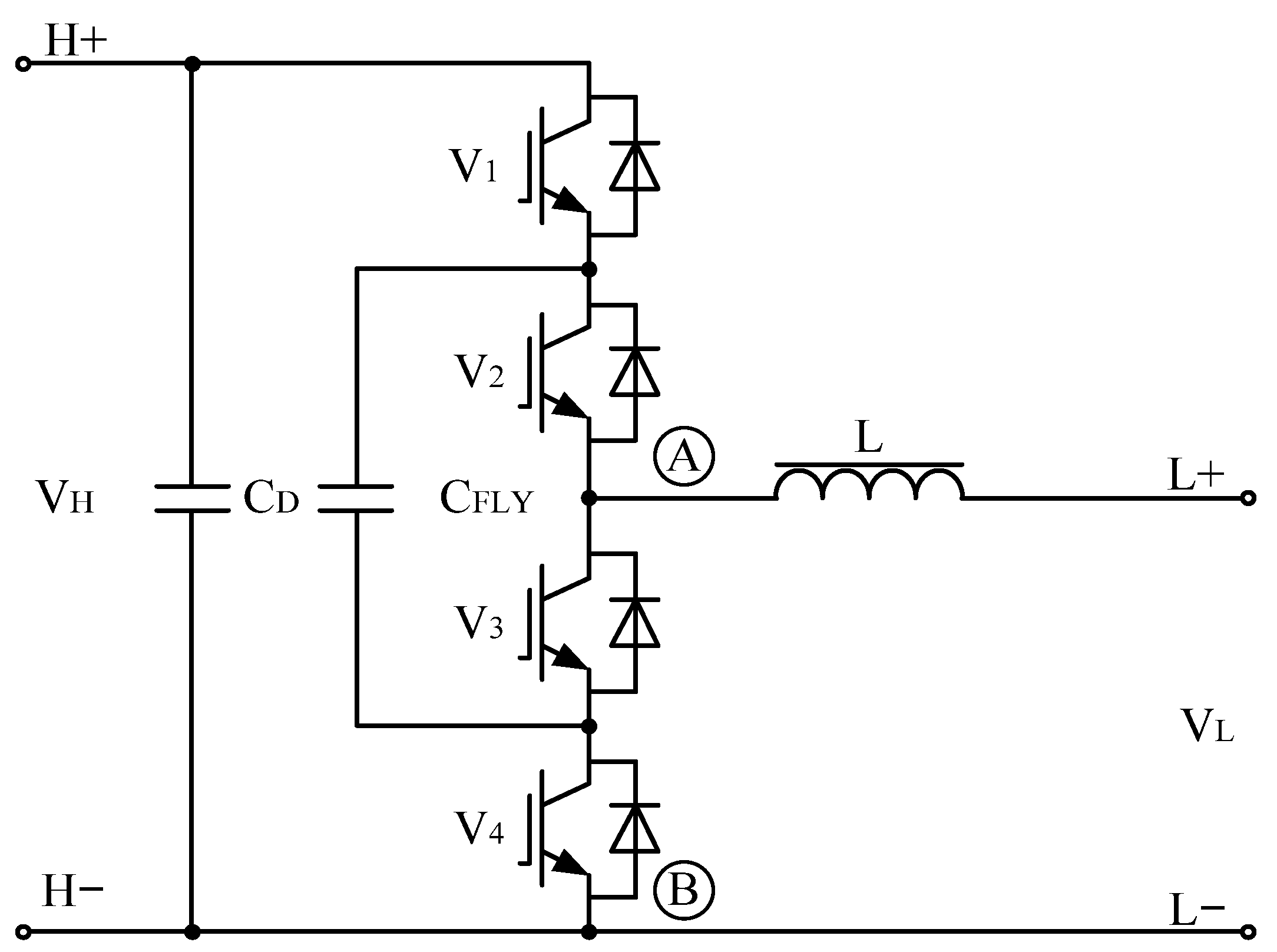
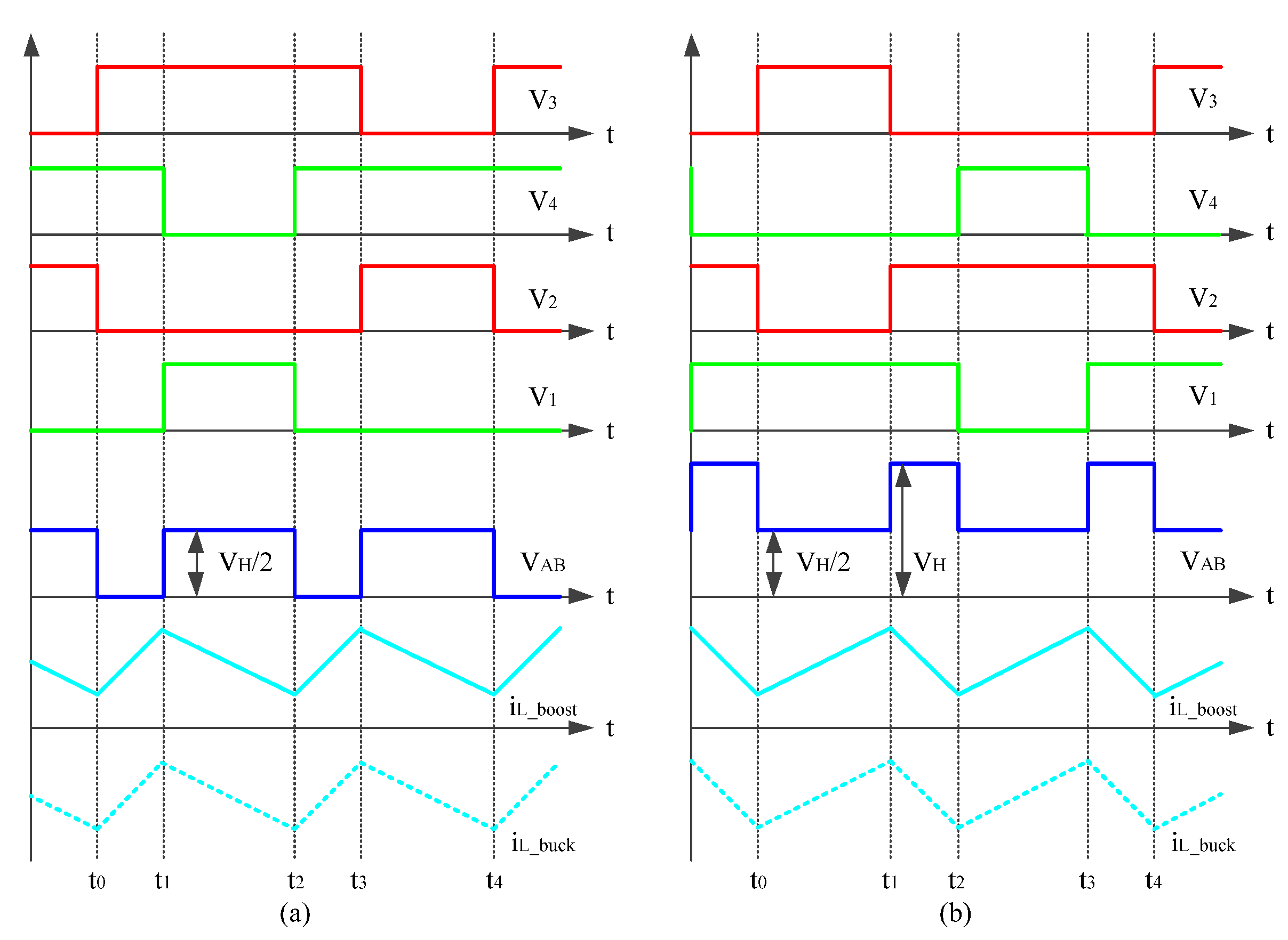
2. Operation Principle of FC-3L-BDC

The topological structure of an FC-3L-BDC is shown in Figure 1. VH is the high side voltage corresponding to the DC bus. VL is the low side voltage corresponding to the energy storage device. CD is the dc-link capacitor. L is the energy storage inductor, and CFLY is the flying capacitor. V1, V2, V3, and V4 are four power semiconductor switches. The drive signals of V1 and V4, V2, and V3 are complementary. The drive signals of V1 and V2, V3, and V4 are alternate, and their carrier shifts 180°.
The FC-3L-BDC can transmit energy in two directions. When the energy flows from VH to VL, it works in buck mode. V1 and V2 are active switches, and V3 and V4 operate in a freewheel state. When the energy flows from VL to VH, it works in boost mode. V3 and V4 are active switches; V1 and V2 operate in a freewheeling state. The only difference between buck and boost modes is that the inductor current is in the opposite direction.
Figure 2 show the key waveforms of an FC-3L-BDC. The voltage conversion ratio of FC-3L-BDC is the same as the two-level buck/boost converter [26].

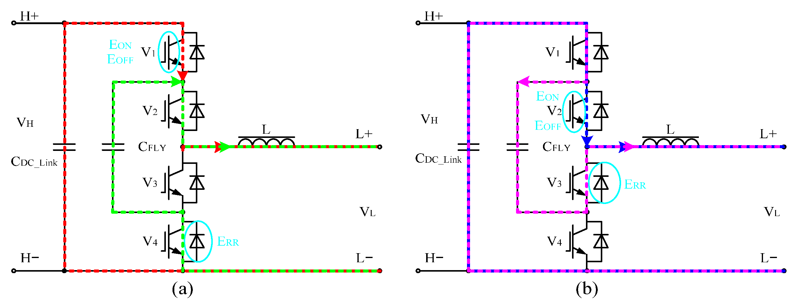
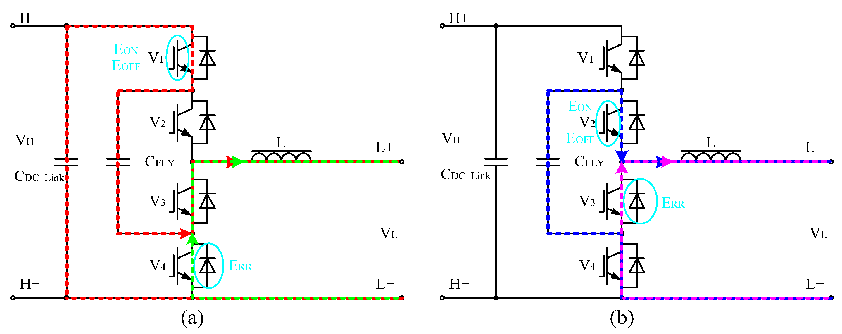
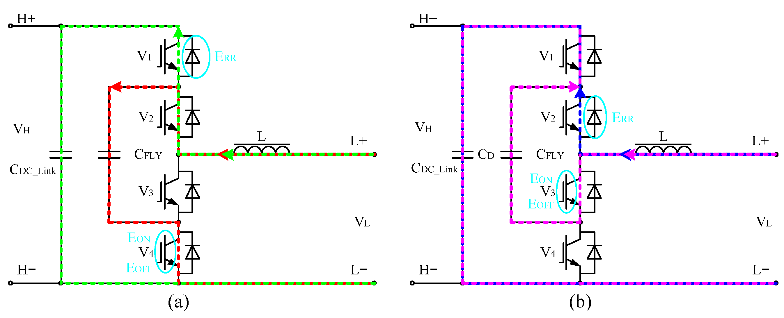
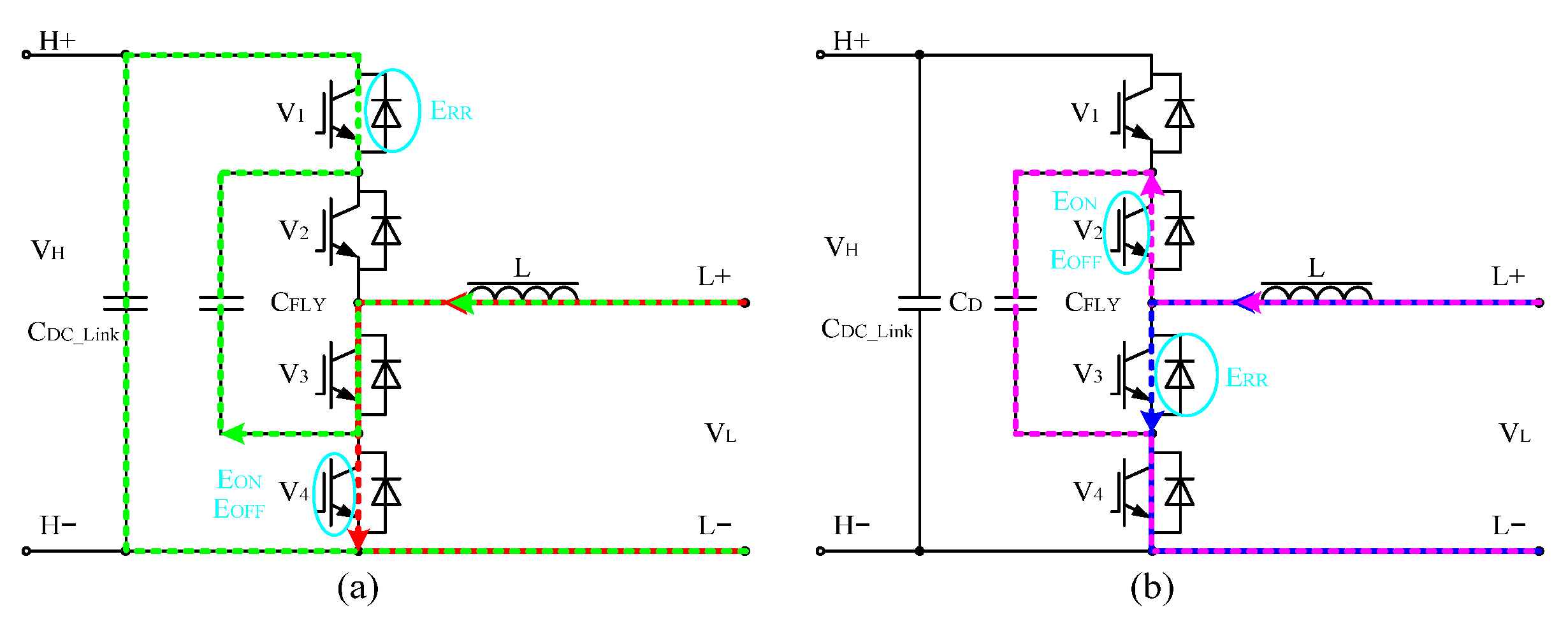
3. Analysis of Commutation Paths of FC-3L-BDC

In the FC-3L-BDC, according to the energy transmit direction and the voltage relationship between the high-voltage side and the low-voltage side, the working modes of the converter can be divided into four different types, as shown in Table 1.

3.1. Commutation Paths

The current paths in different switch statuses in each mode are shown in Figure 3, Figure 4, Figure 5 and Figure 6. In one period, there are three current paths and two commutation paths in each mode. When D < 0.5, the freewheeling current paths are the same for buck and boost modes. When 0.5 < D < 1, the current paths of active switches conducted are the same for buck and boost modes. The current paths of the outer active switches conducted are represented by the red dashed line, and the corresponding freewheeling current paths are represented by the green dashed lines. The loops surrounded by the nonoverlapping paths of the red and green dashed lines are the outer commutation paths in each mode. Similarly, the current paths of the inner active switches conducted are represented by the blue dashed lines, and the corresponding freewheeling current paths are represented by the purple dashed lines. The inner commutation paths are the loops surrounded by the nonoverlapping paths of the blue and purple dashed lines in each mode.
All of the commutation behaviors take place between one IGBT and one FWD. As shown in Figure 3, Figure 4, Figure 5 and Figure 6, the IGBTs and the FWDs, which are marked by a cyan circle, experience turn-on/off losses and reverse recovery losses. Although three devices are involved in the commutation process, only one IGBT experiences turn-on and turn-off, only one FWD experiences reverse recovery, and the remaining IGBT devices continuously conduct current. The active IGBT, the reverse recovery FWD, and commutation paths are shown in Table 2.
As shown in Table 2, there are two different types of commutations with respect to switching loss distribution and stray inductance (Lσ) in each mode. Comparing D < 0.5 and 0.5 < D < 1 for buck mode and boost modes, although the current paths are different as shown in Figure 3, Figure 4, Figure 5 and Figure 6, the switching loss distribution and commutation paths are the same. The current paths and commutation paths in buck mode and D < 0.5 are the same as those in boost mode and 0.5 < D < 1. Similarly, the current paths and commutation paths in buck mode and 0.5 < D < 1 are the same as those in boost mode and D < 0.5.
From the perspective of commutation paths, there are only two paths in all working modes. In Figure 3, Figure 4, Figure 5 and Figure 6, the outer commutation paths are shown by the loops surrounded by red and green dashed lines, and the inner commutation paths are shown by the loops surrounded by blue and purple dashed lines. The Lσ of the outer commutation path (Lσ_O) is always greater than the Lσ of the inner commutation path (Lσ_I) because the length of the outer commutation loop is longer, and both dc-link capacitors and flying capacitors are involved in the commutation process. This paper mainly focuses on the two different types of commutation behavior with respect to Lσ of the commutation path.

3.2. The Influences of Commutation Path Stray Inductance

The switching behavior of IGBTs is always significantly influenced by Lσ.
When the IGBT turns on, a higher Lσ leads to a smaller IGBT collector current slope (diC/dt), a smaller FWD forward current slope (diF/dt), a larger drop in the IGBT collector–emitter voltage when the IGBT collector current sets in, and lower IGBT turn-on losses (Eon). However, the higher the FWD reverse recovery losses (Err) and peak reverse recovery power of FWD, the higher the FWD reverse recovery overvoltage [23].
When the IGBT turns off, a higher Lσ leads to a smaller IGBT collector current gradient (diC/dt), a smaller FWD forward current gradient (diF/dt) before reaching the tail current region, a higher collector–emitter overvoltage, higher IGBT turn-off losses (Eoff), and a less pronounced IGBT collector tail current [23].
Since the inner and outer commutation paths have common paths, the diC/dt of the inner commutation loop during IGBT turning on induces a coupling overvoltage on the IGBT devices of the outer commutation loop, which is in the blocking state, and vice versa. In any case, the voltage of collector–emitter of IGBT devices must not exceed the IGBT blocking voltage.

4. The Design of FC-3L-BDC Phase-Leg PEBB

The FC-3L-BDC phase-leg PEBB was designed for an inductor current of 400 Arms for continuous operating and of 600 Arms for intermittent operating, with a maximum voltage of 1.8 kV on the high-voltage side and 1kV on the low-voltage side. Force-air cooling is used for IGBT heat dissipation of the PEBB. The designed operating temperature range of the PEBB is −30 °C to 50 °C, within which the output power should not be derated up to 2000 m above sea level and the switching frequency of IGBT is up to 2000 Hz. With a single PEBB or several PEBBs, a common DC-link bus and low-voltage side are interleaved parallel, and a 400 kW to MW-grade FC-3L-BDC could be built for light rail vehicle chargers, metro regenerative braking energy recovery, and energy storage converters in DC microgrids. The PEBB design allows the terminals of “H−” or “L−” to connect directly with ground in light rail and metro applications.
The design of a PEBB must satisfy the requirements of isolation voltage, clearance, and creepage distances according to the corresponding standards.

4.1. Selection of IGBT Devices

The new PrimePACK IGBT half-bridge and chopper devices with internal NTC offer a specially optimized concept for integration in modern converters. The most important benefits are improved thermal properties, low stray inductance, and a wide range of operating temperatures, making these devices a preferred choice for a powerful, compact, and modular converter design [27].
The maximum dc-link voltage is 1.8 kV, which leads to a careful consideration of the isolation voltage of all the components in the PEBB in detail. According to [28], for a system voltage of 1.8 kV, the test voltage to verify the dielectric strength is 5 kVrms. The insulation voltage of PrimePACK is 4 kVrms, which cannot directly meet the insulation requirement. In order to meet the insulation requirement, an external insulation strengthening method can be used. In this paper, a floating heat sink is used for improving PEBB isolation to ground. The PEBB is mounted on the cabinet with epoxy structural parts, making the PEBB and heat sink isolated from the system ground. Regarding the selection of the rated voltage of the IGBT device, the DC-link voltage of the converter was mainly considered, and the empirical formula shown in (1) could be used for estimating the blocking voltage of the IGBT device.
V CES = V DC ( 1 + S ) ,
VCES is the collector–emitter voltage of IGBT. VDC is the maximum DC-link voltage. For a three-level topology, VDC is equal to half of the high side voltage. S is the safety margin coefficient. If the stray inductance of commutation paths is small, a safety margin coefficient of 50% should be selected; if the stray inductance of commutation paths is relatively high, a safety margin coefficient of 60% should be selected. The IGBT, whose blocking voltage is above and closest to the calculated value, was finally selected [23]. The designed PEBB operates within a maximum DC-link voltage of 1.8 kV on the high-voltage side. The voltage of the IGBT device in the off state is 900 V, hence the IGBT device with a blocking voltage of 1.7 kV should be used.
The 1.7 kV PrimePACK IGBT devices have three kinds of packages, as shown in Figure 7. The power losses and junction temperature of IGBT devices have been simulated by IPOSIM based on the typical thermal resistance of the force-air cooling and system electrical parameters. Only FF1400R17IP4 with PrimePACK3 package and FF1500R17IP5/FF1800R17IP5 with PrimePACK3+ can meet the application requirements. From the perspective of economy, FF1400R17IP4 with PrimePACK3 package, which is widely used in industry and renewable energy applications, was finally selected.
FF1400R17IP4 can operate with a junction temperature from −40 °C up to 150 °C. The stray inductance of the IGBT package is only 10 nH, covering the path between the upper and lower switch, which is reasonable for two-level converters. In FC-3L-BDC application, two FF1400R17IP4 in series connection constitute an FC-3L-BDC phase leg and directly using the stray inductance given by datasheet underestimates the stray inductance of commutation paths, the reason for which will be analyzed in detail in Section 5.

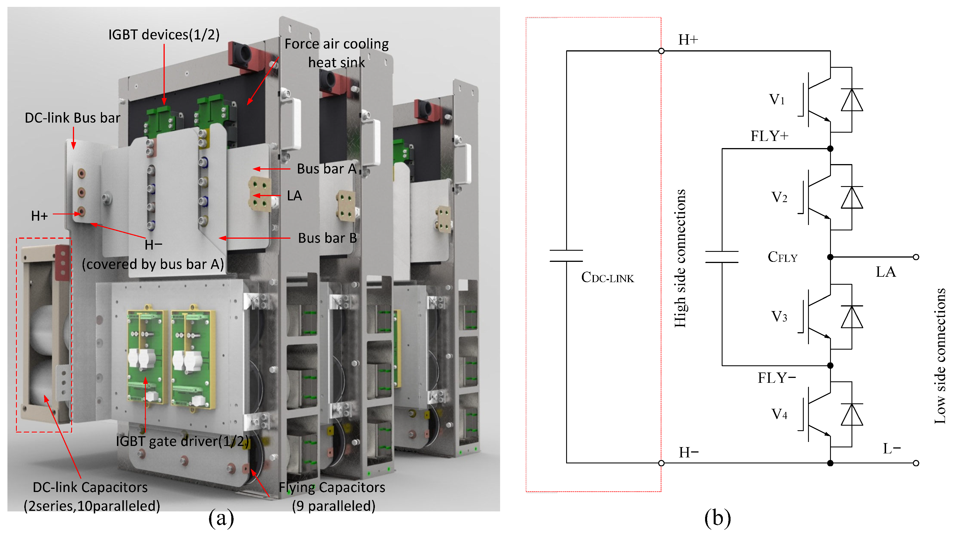
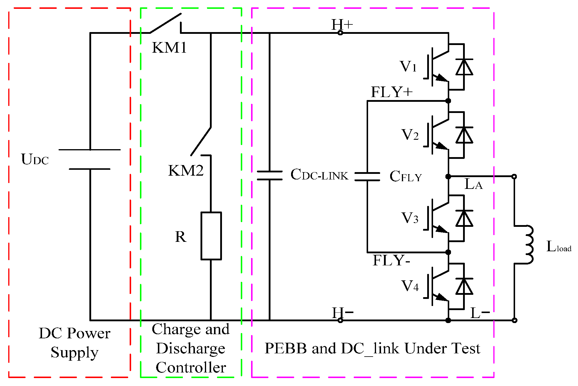
4.2. Description of PEBB

The design of power converters based on the PEBB concept pursues the following three main objectives.
  • Cost effectiveness, by using industry-standardized IGBT devices and metal film capacitors.
  • Production efficiency, by using a laminated bus bar.
  • Maintainability, by using force-air cooling and a single phase-leg configuration. Only the flying capacitors are integrated in the PEBB. The high-voltage-side DC-link capacitors are installed in the converter cabinet. In this approach, the weight of the PEBB can be minimized.
Figure 8a shows the 3D models of the PEBB, the DC-link capacitors, and the DC-link bus bar. The PEBB contains the following elements: IGBT devices, IGBT gate drivers, laminate bus bars, the heat sink, and flying capacitors. Figure 8b shows the simplified electrical scheme of the PEBB, and the capacitors marked by the red dotted box are DC-link capacitors and the DC-link bus bar, both of which are installed in the converter cabinet. The DC-link capacitors are composed of 20 metalized polyethylene capacitors with 0.92 mF, 1100 V, and 90 A for each capacitor, and these capacitors are arranged in a 10p2s configuration (10 capacitors in parallel and 2 capacitors in series).
The entire power interconnections of the PEBB are composed of two laminated bus bars, “A” and “B”. The designed isolation voltage between any layers of bus bar A is 6 kVrms, since the differential voltage between the layers is 1.8 kV in normal operation. The designed isolation voltage between the two layers of bus bar B is 4 kVrms because the differential voltage between the two layers is 0.9 kV in normal operation. The laminated bus bar of B is mounted on top of the laminated bus bar of A. Two rows of copper rings riveted on the laminated bus bar of A are used for connecting the high-voltage side of the PEBB to the common dc-link of the converter. The laminated bus bar of A has an L-shaped terminal, which is used for connecting the PEBB to the filter inductor of the low-voltage side. The laminated bus bars have been manufactured by ROGES CORP. The flying capacitor is composed of six parallel metalized polyethylene capacitors with 0.4 mF, 1100 V, and 60 A for each capacitor. The flying capacitors and two half-bridge IGBT devices are connected by bus bar B.
The stray inductance Lσ of commutation paths is the most important parameter for designing the power interconnection of the PEBB. An excessively high stray inductance can cause an IGBT turn-off and FWD reverse recovery voltage spike to exceed the blocking voltage of the IGBT device and increase the EMI. In the condition of high Lσ, high DC-link voltage, high current, and low junction temperature, the IGBT produces the highest turn-off overvoltage. In the condition of high Lσ, high DC-link voltage, low forward current, and low junction temperature, it is likely that the fast-recovery power diode produces excessive voltage spikes due to snappy recovery. These effects can destroy the IGBT and FWD, which ultimately causes a circuit failure [29]. If a turn-off voltage spike exceeding the blocking voltage or snappy recovery is detected, it requires reducing the IGBT turn-on/off speed or adding snubber circuits. Both measures are not desired in the process of the PEBB design because these measures often induce more power losses in IGBT devices or snubber circuits, which also increase the cost and complexity of the system. Therefore, the PEBB was designed without snubber circuits.
To realize snubberless operation, the stray inductance of each commutation path must be minimized. Decreasing the self-stray inductance of each current path and increasing the mutual inductance among the current paths in which the switching current flows in opposite directions are effective approaches. The copper planar sheets are used as conductors in each layer because the copper planar sheet has less self-stray inductance than wire [30]. In order to further decrease the stray inductance, copper planar sheets with opposite commutation current directions are grouped together, taking advantage of the subtractive mutual inductance reducing the overall stray inductance of commutation paths. The equivalent stray inductance of a set of two coupled conductor layers, “1” and “2”, can be shown as follows [30]:
L σ 12 = L σ 1 + L σ 2 + 2 M σ 12 ,
where Lσ1 and Lσ2 are the self-stray inductance of each conductor layer and Mσ12 is the mutual coupling inductance between layers. If the current in “1” and “2” flows in opposite directions, the mutual coupling inductance is negative. It is clear that the overlap between the conductor layers is the key point to obtaining a laminated bus bar with low overall stray inductance. The following principles are the design reference of how to determine the placement of the IGBT devices.
  • A symmetrical layout should be adopted. Actually, if the placement direction of IGBT devices is consistent and aligned, the symmetry of the layout can be guaranteed.
  • Reduce the difference in stray inductance between the outer and inner commutation paths. Reduce Lσ_O as much as possible.
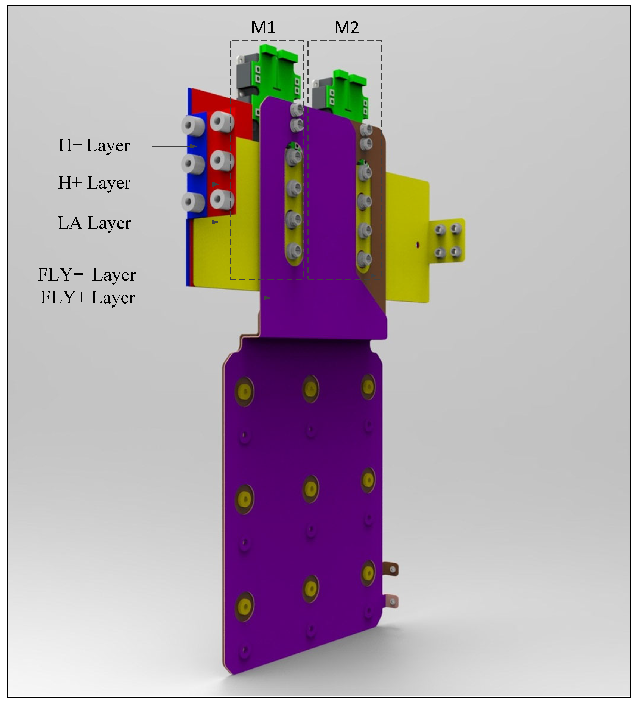
  • Completely overlap the copper planar sheets in each layer.
  • Since the commutation current directions of “H−” and “H+” layers are opposite, the two layers should be arranged next to each other.
  • Since the commutation current directions of “FLY+”, “FLY−”, and “LA” layers are opposite, the three layers should be arranged next to each other.
The final placement of IGBT devices and the polarity placement of the bus bar are shown in Figure 9. The IGBT is denoted as “Mn”, where “n” goes from 1 to 2. The half-bridge IGBT device M1 corresponds to V1 and V2 shown in Figure 8. The half-bridge IGBT device M2 corresponds to V3 and V4 shown in Figure 8.
The three-layer bus bar A is mounted on IGBT devices, and the two-layer bus bar B is overlapping with bus bar A. The five-polarity conductor plates are shown in different colors. The conductor planar sheets, from bottom to top, are “H−” (red), “H+” (blue), “LA” (yellow), “FLY−” (brown), and “FLY+” (purple).
The IGBT devices are mounted on the heat sink. Each IGBT device is controlled by a self-designed IGBT gate driver with a 0.9 Ω turn-on gate resistor, 1.6 Ω turn-off gate resistor, +15 V turn-on gate–emitter voltage, and −15 V of turn-off gate–emitter voltage.

4.3. Clearance and Creepage Distances

The power converter was designed for a nominal voltage of 1.8 kV. According to [28], the minimum value of the required rated insulation voltage is 1.8 kV, and overvoltage category III (OVC III) is applied since the circuits are powered by a contact line but with less harsh overvoltage. The clearance and creepage distances of PEBB must conform to the corresponding standard, the values of which depend on the electrical surge, the protection measures, and the pollution of the installation place. Clearance distances are dimensioned by the rated impulse voltage and pollution degrees. The rated impulse voltage is defined by the rated insulation voltage and overvoltage category. According to [31], for a rated insulation voltage of 1.8 kV and OVC III, the corresponding impulse voltage is 10 kV, and a minimum clearance distance of 11mm is required for equipment up to 2000 m above sea level. Creepage distances are determined by the working voltage, the comparative tracking index (CTI) of insulating materials, and the pollution degree. Creepage distances should be large enough to prevent long-term degradation of the surface of solid insulators. For a system voltage of 1.8 kV and a pollution degree of level 3, a minimum creepage distance of 18 mm is required for material groups III (175 ≤ CTI < 400). For all the customized components present in the PEBB and in the final power converter, a minimum clearance of 11 mm and a minimum creepage distance of 18 mm are required.

5. Stray Inductance Estimation

In this section, to estimate the stray inductances (Lσ) of commutation paths of PEBB, a 3D model was established on the basis of the physical layout. The parasitic parameters of commutation paths were extracted by 3D-FEM software, which is based on a simplification of Maxwell’s equation called the quasistatic approximation. In this way, it is assumed that the size of the underanalysis structure is small compared to the wavelength at the maximum frequency of interest. A general rule of thumb is that the size of the structure should be less than one-tenth of the wavelength. The highest frequency component in the PEBB determines the critical frequency of the system [30]. In this case, this frequency corresponds to the rise time (tr) of the FF1400R17IP4 IGBT device used in PEBB, which, from the manufacturer’s given information, is around 0.13 μS, imposing a critical frequency (fc = 1/(2‧π‧tr)) around 1.22 MHz. One-tenth of the critical component wavelength is 24.5 m, which is far greater than any point-to-point distances within the PEBB and converter. Under the quasistatic approximation, the coupling between magnetic and electric fields can be neglected, and this assumption allows the software to solve very complicated structures in an efficient way. If the structure is larger than one-tenth of the wavelength, a full-wave field solver which considers the two-way coupling between the electric and magnetic fields can be used. In order to extract the inductance corresponding to the actual working frequency, a frequency sweep simulation is performed, and the inductance at the critical frequency of the system is extracted.

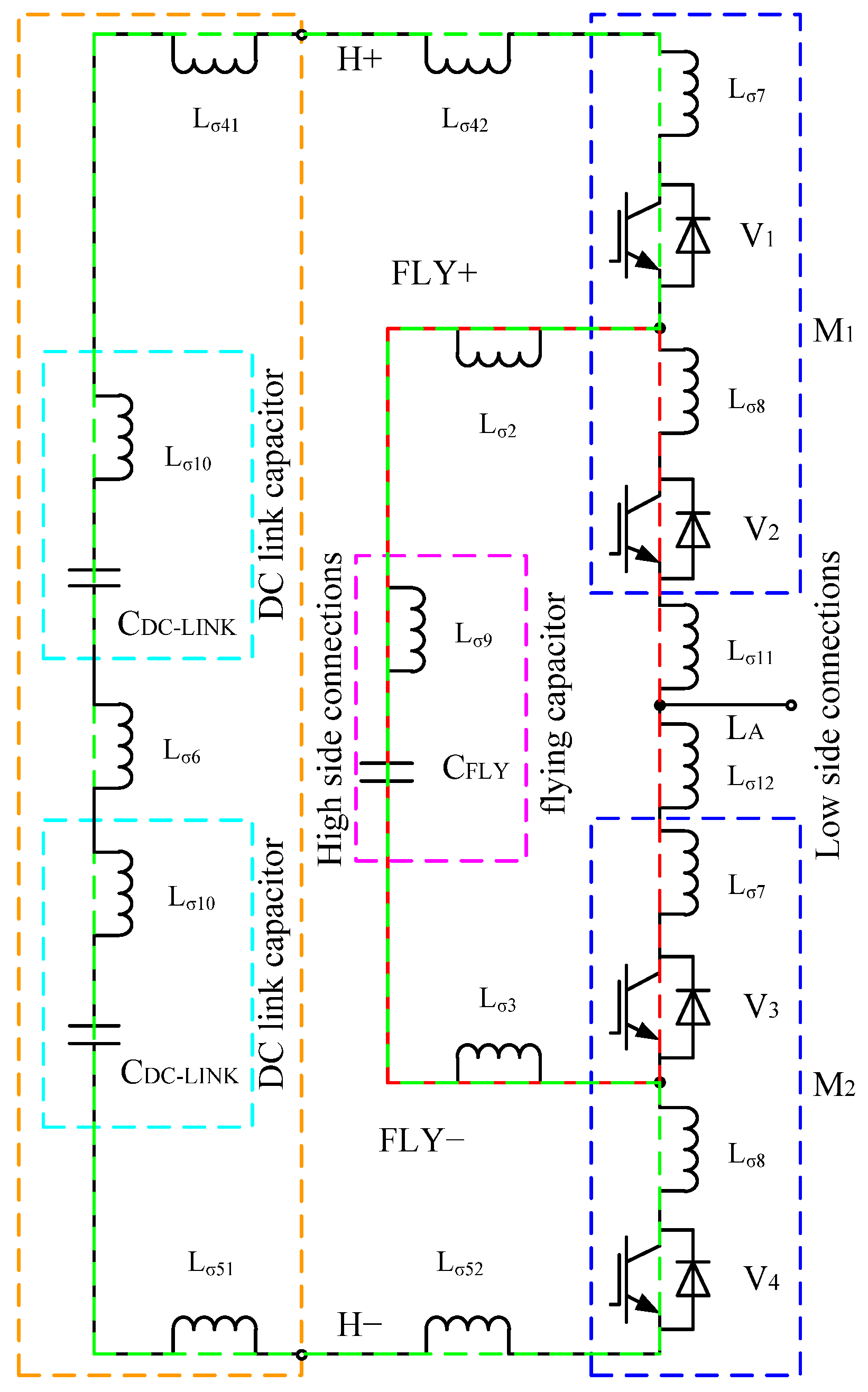
5.1. Lumped Stray Inductance Model of PEBB with Mutual Coupling Consideration

Whether a lumped parameter model or a transmission line model is required to analyze a bus bar stray inductance is determined by the critical frequency in the PEBB. A transmission line model is required when the longest point-to-point current path of a bus bar is larger than a quarter of the critical component wavelength (λc = c/fc) [30]. For a critical frequency of 1.22 MHz, a quarter of the wavelength is 61.5 m; the length is far greater than any point-to-point distance within bus bars, so using the lumped stray inductance model is adequate.
Since the capacitor, bus bar, and IGBT are not ideal electronic devices, they have parasitic resistance, parasitic capacitance, and stray inductance, where the effects of parasitic resistance and parasitic capacitance on the commutation behavior of the IGBT can be neglected and only their stray inductance is considered. According to the electrical scheme of FC-3L-BDC in Figure 8, a lumped stray inductance model can be obtained as shown in Figure 10.
Where Lσ1 (sum of Lσ11 and Lσ12) is the stray inductance of path LA; Lσ2 is the stray inductance of path FLY+; Lσ3 is the stray inductance of path FLY−; Lσ4 (sum of Lσ41 and Lσ42) is the stray inductance of the path H+; Lσ5 (sum of Lσ51 and Lσ52) is the stray inductance of path H−; Lσ6 is the stray inductance of the connection between the series DC-link capacitors (the path is named CC); Lσ7 is the stray inductance of the upper switch of the IGBT device; Lσ8 is the stray inductance of the lower switch of the IGBT device; Lσ9 is the flying capacitor inductance; and Lσ10 is the internal stray inductance of the dual dc-link capacitor. As shown in Figure 10, the inner and outer commutation paths are shown in red and green dashed loops, respectively.
Mσij is the mutual inductance between any two components within the PEBB, which is not shown in Figure 10. i is not equal to j, and i and j are less than six.

5.2. Estimation of Stray Inductance of Laminated Bus Bars

Stray inductances of bus bars in each commutation loop are extracted by 3D-FEA simulations, taking into account the mutual inductance of each polarity layer. Usually, shorting the cooper planar sheets in each commutation path by adding a short-connect conductor with only two terminals open and extracting the stray inductance of the loop from the two open circuit terminals are used to extract the stray inductance of commutation paths. It is obvious that stray self-inductance of the short-connect conductors and the mutual inductance between the short-connect conductors and the cooper planar sheets of bus bars lead to an inaccurate result. In this paper, an inductance matrix extracting method is used; the sink and source for each cooper planar sheet were separately assigned according to the direction of commutation current, and the stray self-inductance and mutual stray inductance matrix between each cooper planar sheet were extracted by simulation. In this way, the structure of bus bars is not changed, so the result is more accurate. Table 3 and Table 4 show the stray self-inductance and mutual inductance matrix of each polarity’s cooper planar sheets of the bus bar of PEBB at the critical frequency. The parameters on the diagonal in the table are the self-inductance of each current path, and the other parameters are the mutual inductance between the current paths.
Similar to (2), the effective stray inductance of bus bars in each commutation path is calculated according to stray self-inductances and stray mutual inductances of copper planar sheets. Effective stray inductances of inner and outer loops of bus bars are shown as follows:
L σ _ I _ B B = i = 1 3 L σ i + 1 i , j 3 , i j M σ i j = 23.87 n H ,
L σ _ O _ B B = i = 2 5 L σ i + 2 i , j 5 , i j M σ i j = 37.67 n H ,

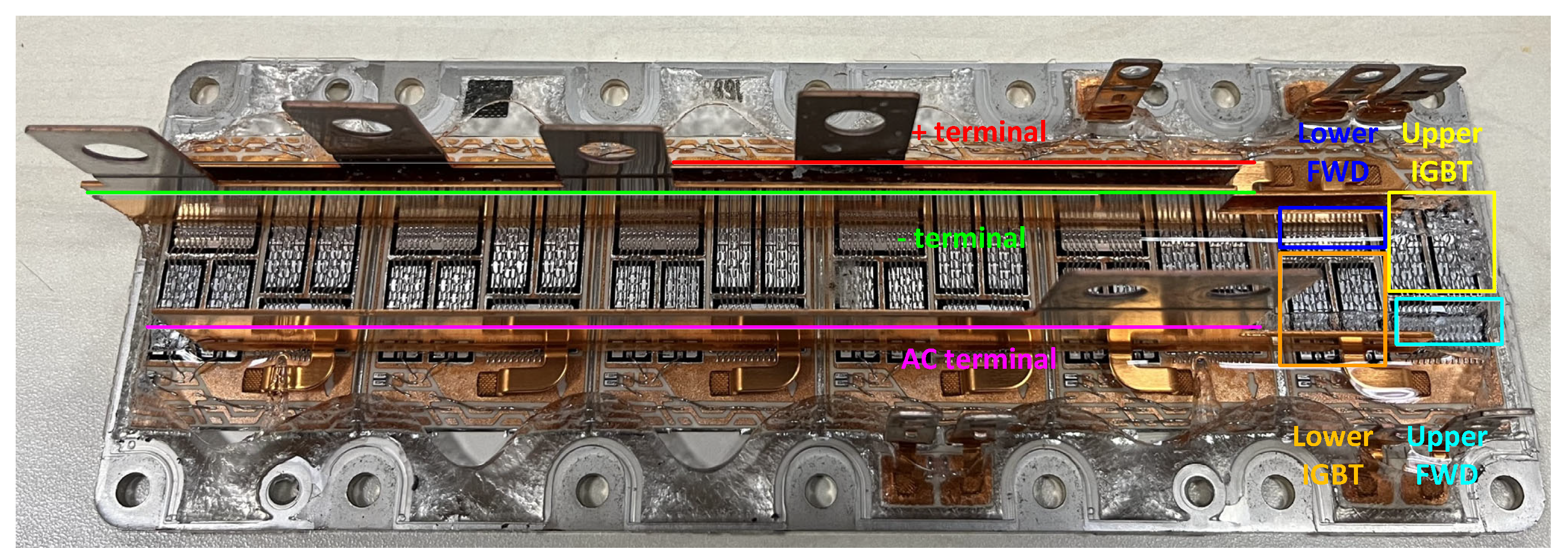
5.3. Stray Inductance of IGBT

The stray inductance of a half-bridge device given by the datasheet covers the full commutation loop between the upper and lower switches. As shown in Figure 11, the chips (IGBT and FWD) of upper and lower switches in PrimePACK3 are arranged as close as possible, and the power connections of “+” and “−” terminals are overlapped, while the distance between the AC, “−”, and “+” terminals is about 20 mm to 23 mm. In two-level converter applications, the commutation path in the IGBT device is from the terminal “+” to “−”, so the stray inductance is extremely low. In the FC-3L-BDC application, the IGBT devices involved in the outer and inner commutation loops are not in the same half-bridge package. Actually, the commutation path in the IGBT devices is from the terminal “+” to terminal “AC” for V1 and V3 and from the terminal “AC” to terminal “−” for V2 and V4, which is different from the test condition of stray inductance given by the datasheet. Therefore, the stray inductance of IGBT devices with a half-bridge package in an FC-3L-BDC application must be retested.
There are two ways to estimate the stray inductance of an IGBT device. The 3D-FEA method is usually used in the design process of an IGBT package. Due to the lack of a precise 3D model, a stray inductance extracting method based on measuring the voltage drop of the diode and the value of diF/dt during the process of diode reverse recovery is used in this paper, as shown in Figure 12.
The stray inductance is extracted during a time interval where the diF/dt is constant and the diode still has not attained its blocking capability, so the voltage drop can only be caused by the stray inductance of the IGBT device. The stray inductance of the IGBT device is calculated according to (5) [32]. Actually, the value of diF/dt is not completely constant during IGBT turn-on and diode reverse recovery transitions, so the result can be influenced by the selection of calculation interval and noise. Taking the integral of the numerator and denominator on the right side of (5) can significantly reduce the influence of calculation interval and noise and obtain more accurate results, so this method could be extended to the measurements of the stray inductance of capacitors, commutation paths, etc.
L I G B T = Δ V C E d i C / d t ,
L I G B T = t 0 t 0 + Δ t Δ V C E d t t 0 t 0 + Δ t ( d i C / d t ) d t = t 0 t 0 + Δ t Δ V C E d t i C ( t 0 + Δ t ) i C ( t 0 ) ,
Voltage and current waveforms during diode reverse recovery are shown in Figure 13. It is important to note that the upper and lower testing switches must be in two separate packages, or the mutual inductance between the terminals “+” and “−” in the half-bridge package leads to underestimated test values.
Stray inductances of the upper switch (Lσ_upper) and the lower switch (Lσ_lower) of FF1400R17IP4 can be obtained as follows:
L σ _ L O W E R = t 0 t 0 + Δ t Δ V C E _ V 2 d t i C _ V 2 ( t 0 + Δ t ) i C _ V 2 ( t 0 ) = 8.934 × 10 6 0.5 ( 503.75 ) = 17.8 n H ,
L σ _ U P P E R = t 0 t 0 + Δ t Δ V C E _ V 3 d t i C _ V 3 ( t 0 + Δ t ) i C _ V 3 ( t 0 ) = 8.928 × 10 6 3.4375 ( 501.25 ) = 17.9 n H ,

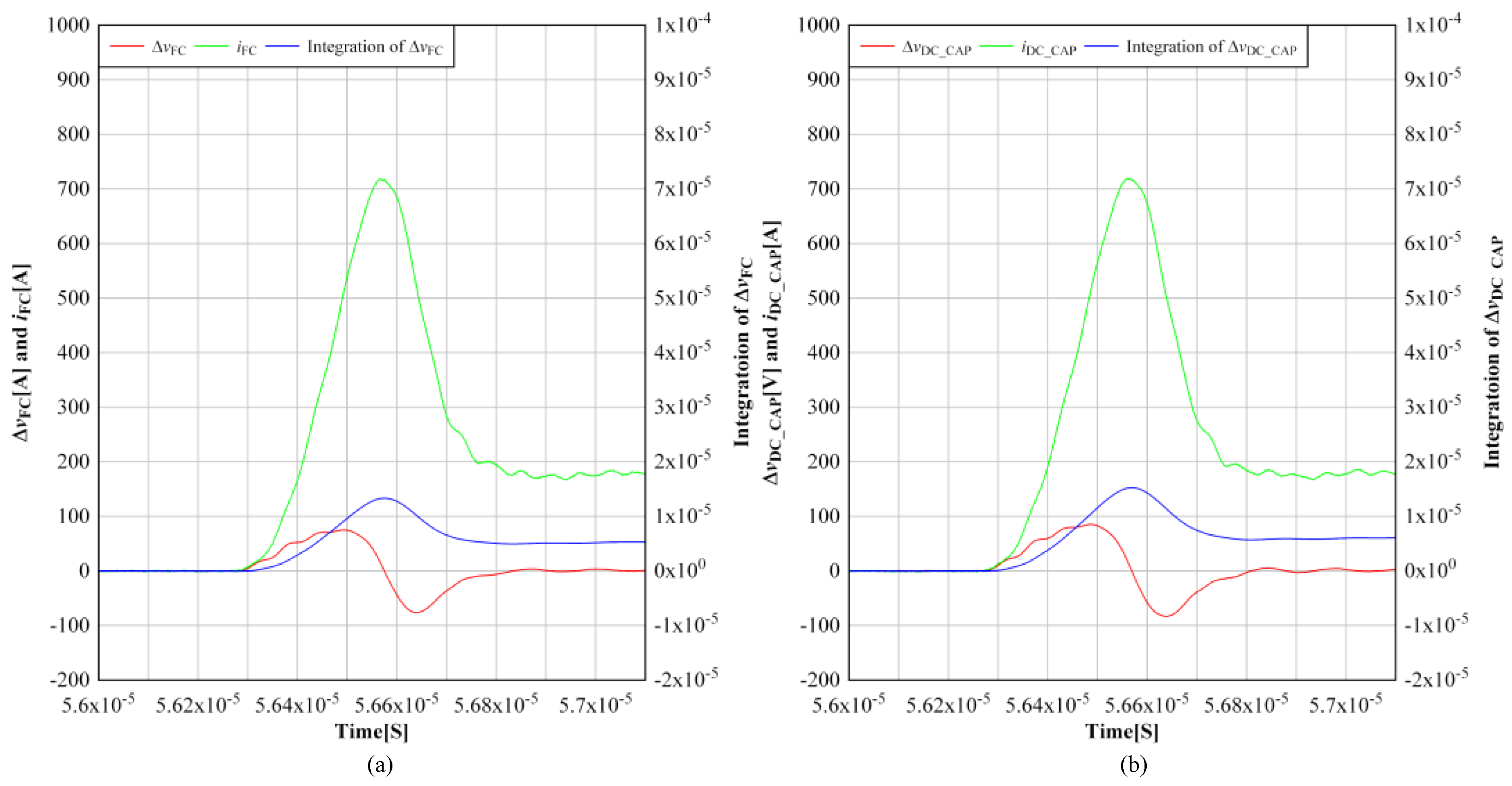
5.4. Stray Inductance of Flying Capacitor and DC-Link Capacitor

Usually, the stray inductance of a capacitor given by the datasheet is based on the resonance frequency measuring method [33]. This stray inductance is the maximum value for the product routine test and can only correctly reflect the characteristic of capacitors near resonance frequency, which is different from the critical frequency of the system corresponding to IGBT switching.
There are also two ways to extract the stray inductance corresponding to the critical frequency of the system. The first method is based on the double-pulse test, measuring the voltage variation and the current slope of the capacitor during IGBT turn-on and calculating the stray inductance base on (9). The second one is based on impedance analysis with a precise impedance analyzer machine. The E4990A fabricated by Keysight is used in this paper. A test fixture was used for flying capacitor and DC-link capacitor measurements, which could execute open and short compensations to eliminate the effects of the test fixture’s residuals for accurate measurements [34]. Both methods are used for extracting and cross-checking the flying capacitor and DC-link capacitor stray inductance.
L σ _ c a p a c i t o r = Δ V c a p a c i t o r d i c a p a c i t o r / d t = t 0 t 0 + Δ t Δ V c a p a c i t o r d t i c a p a c i t o r ( t 0 + Δ t ) i c a p a c i t o r ( t 0 ) ,
As shown in Figure 14, during the IGBT turn-on transition, there are capacitor voltage and current variations. The capacitor voltage is captured by an oscilloscope set on AC coupling for more accurate measurement. Stray inductances of the flying capacitor and DC-link capacitor can be calculated from (10) and (11), and the calculation time interval is selected in an interval with a relatively constant diF/dt.
L σ _ F C = t 0 t 0 + Δ t Δ V F C d t i F C ( t 0 + Δ t ) i F C ( t 0 ) = 5.775 × 10 6 601.64 302.95 = 19.33 n H ,
L σ _ D C _ C A P = t 0 t 0 + Δ t Δ V D C _ C A P d t i D C _ C A P ( t 0 + Δ t ) i D C _ C A P ( t 0 ) = 6.7 × 10 6 605.08 303.78 = 22.24 n H ,
Figure 15 shows the impedance and phase angle of effective stray inductances of the flying capacitor and DC-link capacitor in the frequency range of 100 Hz to 100 MHz.
The effective stray inductance at the critical frequency can be obtained from the impedance curves, and the stray inductance based on the resonance frequency can be derived as follows [33]:
L σ _ c a p a c i t o r = 1 ( 2 π f ) 2 C c a p a c i t o r ,
Stray inductances of the flying capacitor and DC-link capacitor with different measurement methods are listed in Table 5.
It can be seen that the stray inductances extracted by double-pulse tests and impedance analysis at the critical frequency are almost the same, and they are much smaller than the value extracted by the resonance method.

5.5. Effective Stray Inductance of Commutation Loop

For the inner and outer commutation paths of a phase leg of PEBB, the effective stray inductance of bus bars can be calculated from (3) and (4), respectively. Due to the lack of precise 3D models of IGBT and capacitors, 3D-FEA simulations obviate the mutual coupling between capacitors, IGBT devices, and bus bars. Since capacitors and IGBT devices are overlapped by bus bars, the mutual coupling should not be completely neglected. In the case of stray inductance measurement by the double-pulse testing method, the measurement circuit of an IGBT device and capacitors is similar to the real application, so the mutual coupling was taken into account in the stray inductance extracted by double-pulse tests. Taking into account that the stray inductance of several parallel capacitors is equal to the stray inductance of a single capacitor divided by the number of capacitors, the stray inductance can be obtained as the sum of stray inductances of flying capacitors, IGBT devices, and the inner loop bus bars in the inner commutation loop, as shown in (13). Similarly, in the outer commutation loop, the stray inductance can be obtained as the sum of stray inductances of dc link capacitors, flying capacitors, IGBT devices, and the outer loop bus bars, as shown in (14).
L σ _ I = L σ _ I _ B B + L σ _ L O W E R _ I G B T + L σ _ U P P E R _ I G B T + 1 9 L σ _ F C = 61.72 n H ,
L σ _ O = L σ _ O _ B B + L σ _ L O W E R _ I G B T + L σ _ U P P E R _ I G B T + 2 10 L σ _ D C _ C A P + 1 9 L σ _ F C = 79.97 n H ,

6. Experimental Results

In order to verify the commutation behavior and stray inductance analysis, double-pulse tests under three different virtual junction temperatures (Tvj) of −40 °C, 25 °C, and 150 °C were carried out. In addition, short circuit tests of inner and outer commutation paths were performed to prove the robustness of the PEBB design.

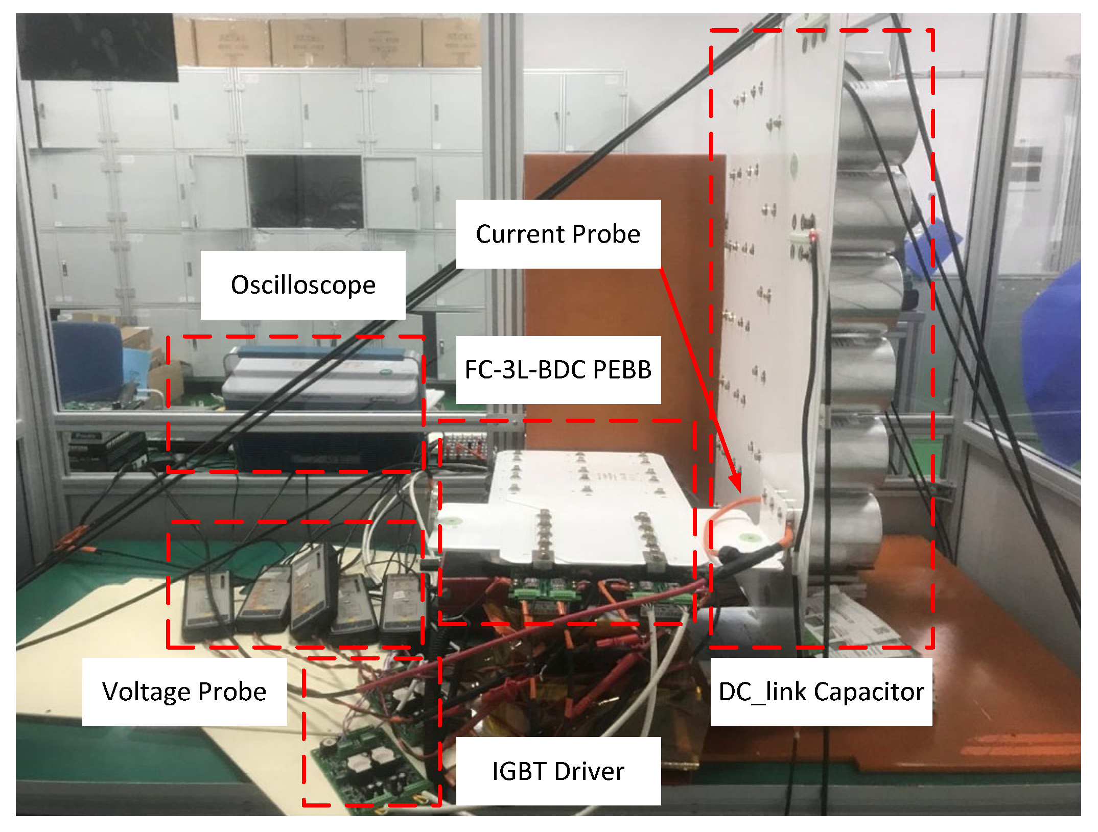
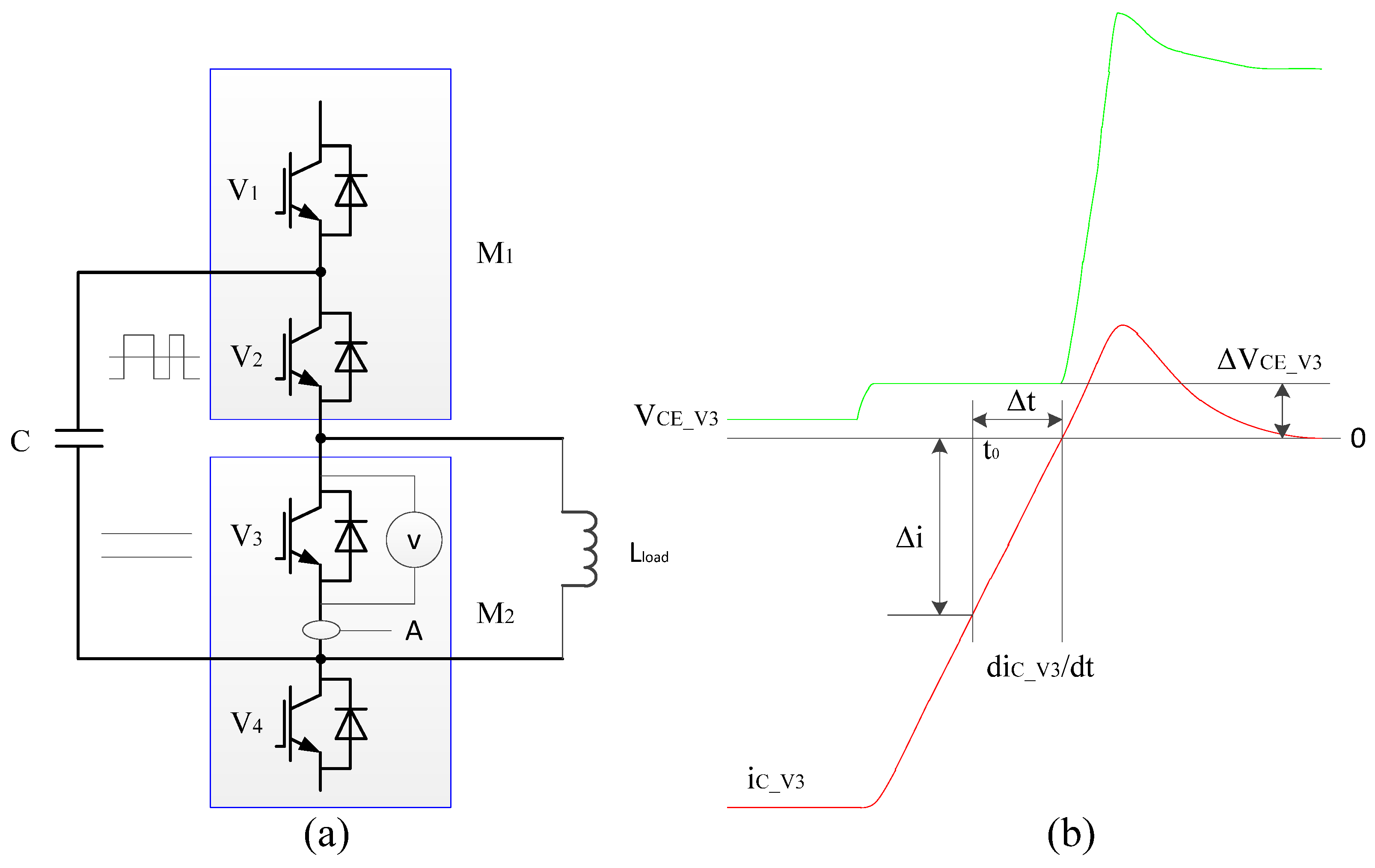
6.1. Test Bench Description

The test bench is composed of a high-voltage DC power supply, heating system, measurement system, inductive load, and other accessories, as shown in Figure 16. The heater is placed under IGBT devices.

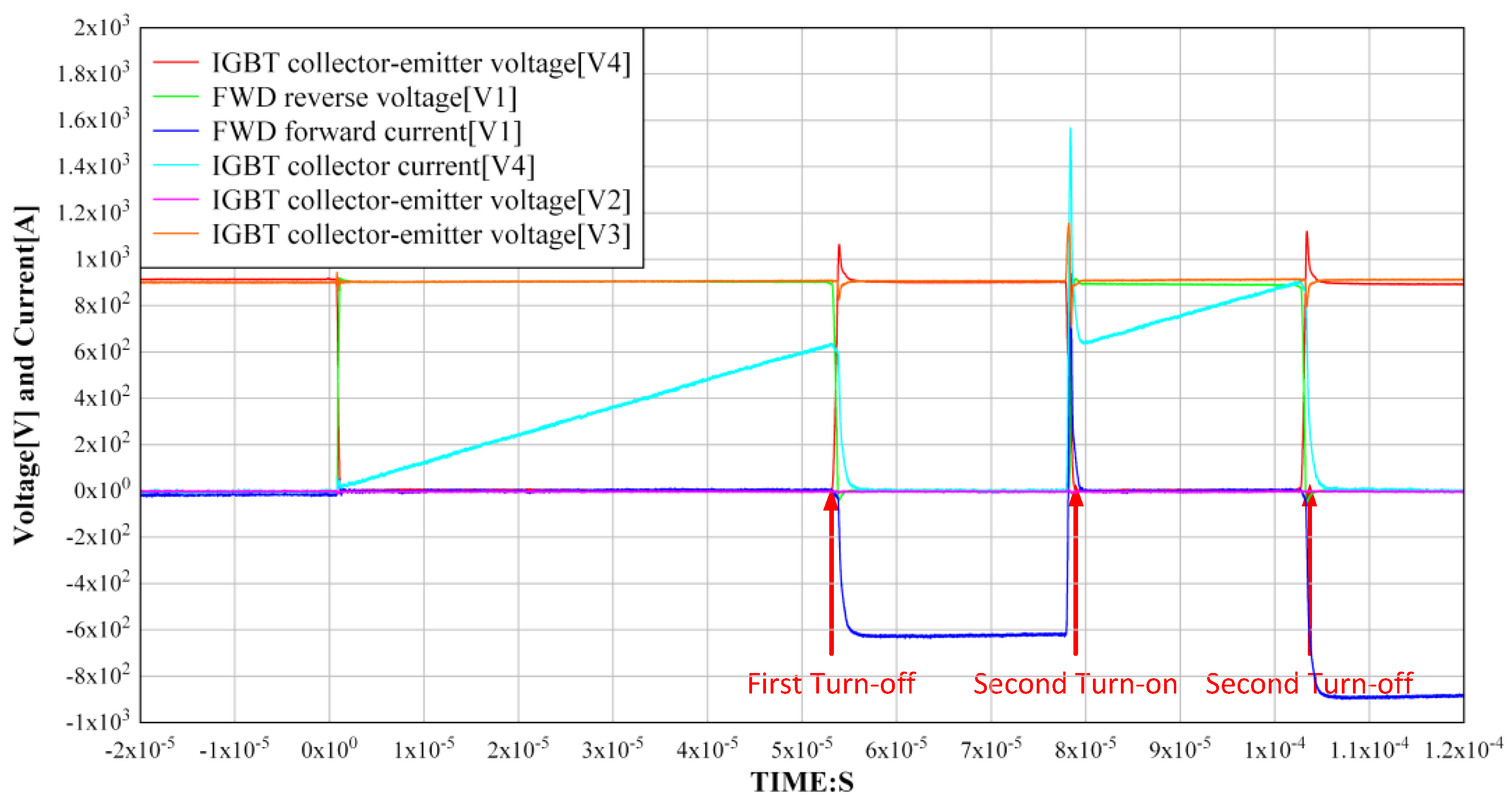
6.2. Double-Pulse Test for the FC-3L-BDC Phase-Leg PEBB

A simplified schematic of the test bench configuration for the double-pulse test in buck mode of FC-3L-BDC is shown in Figure 17.
In a double-pulse test, the first turn-off is used for analyzing the IGBT turn-off behavior, and the second turn-on is used for characterizing the IGBT turn-on and FWD recovery behaviors. Typical waveforms of a double-pulse test are shown in Figure 18.
As discussed in Section 5.2, to correctly measure values of stray inductances, double-pulse tests were performed based on the actual PEBB circuit instead of relying on stray inductance values given by the IGBT modules datasheet. In order to perform double-pulse tests for all commutation paths, the gate signals for the IGBT devices are adjusted, as listed in Table 6. As shown in Figure 17, the inductive load is connected between the terminal LA and the terminal H− for buck mode commutation path characterization. For boost mode commutation path characterization, the inductive load is connected between the terminal LA and the terminal H+.

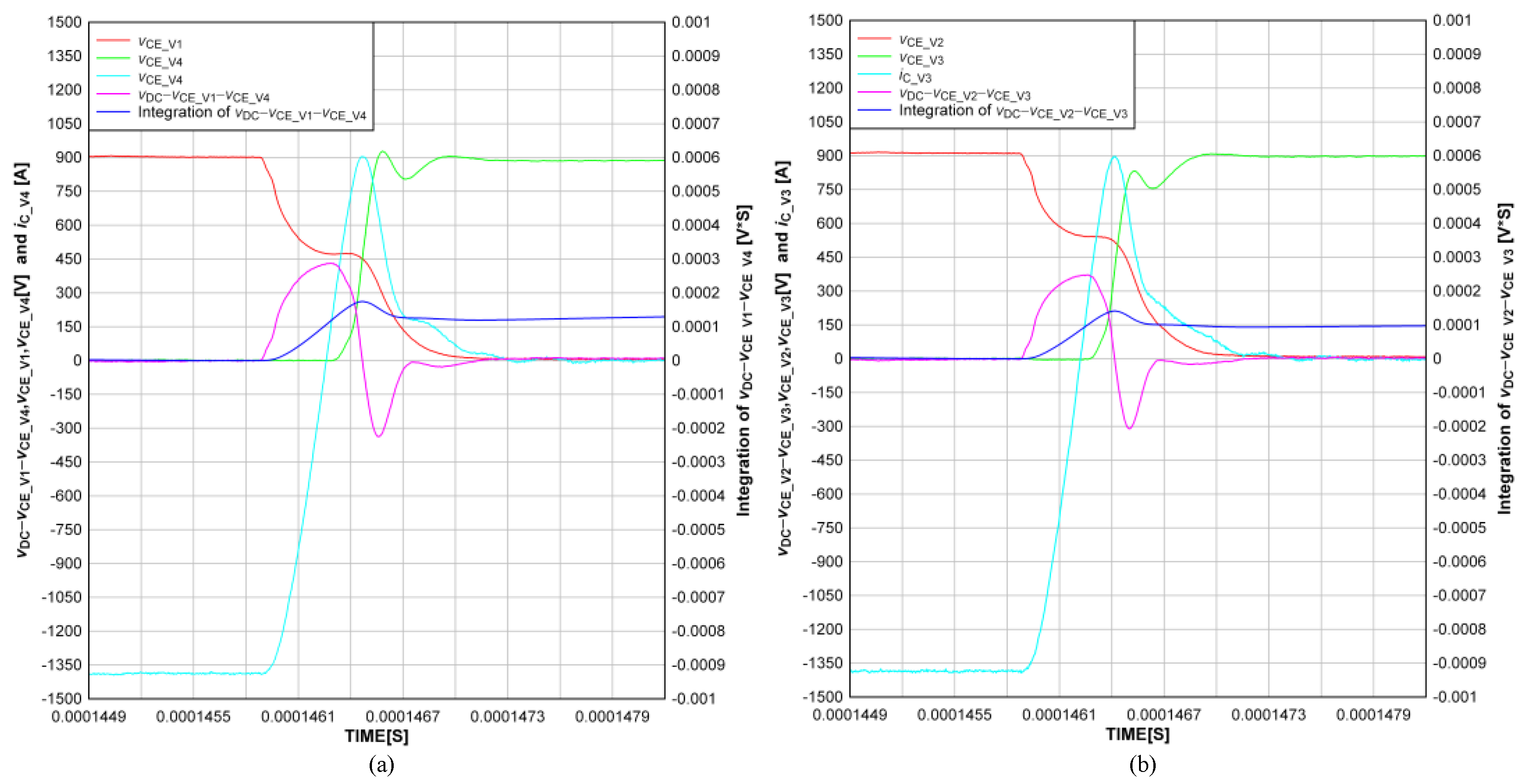
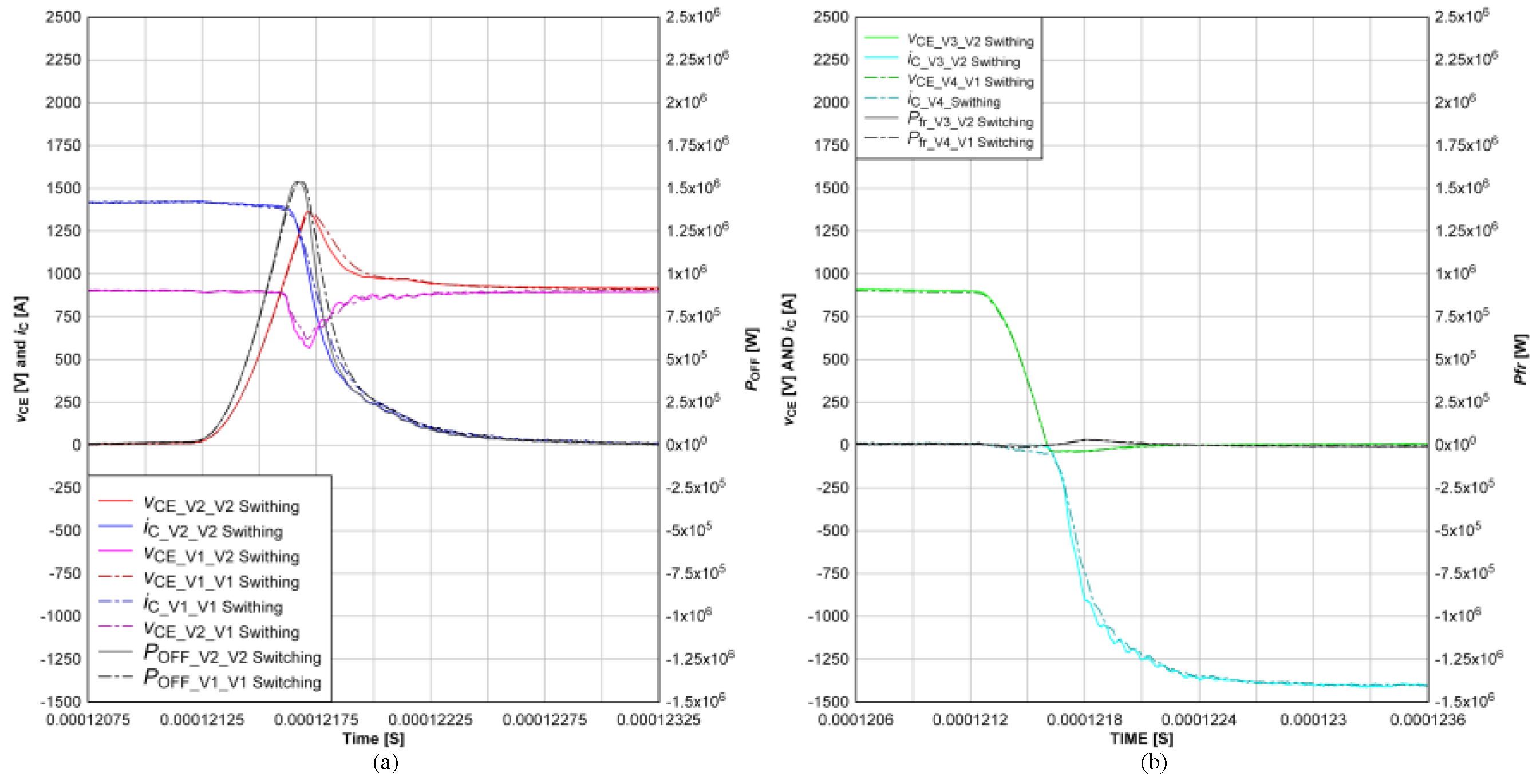
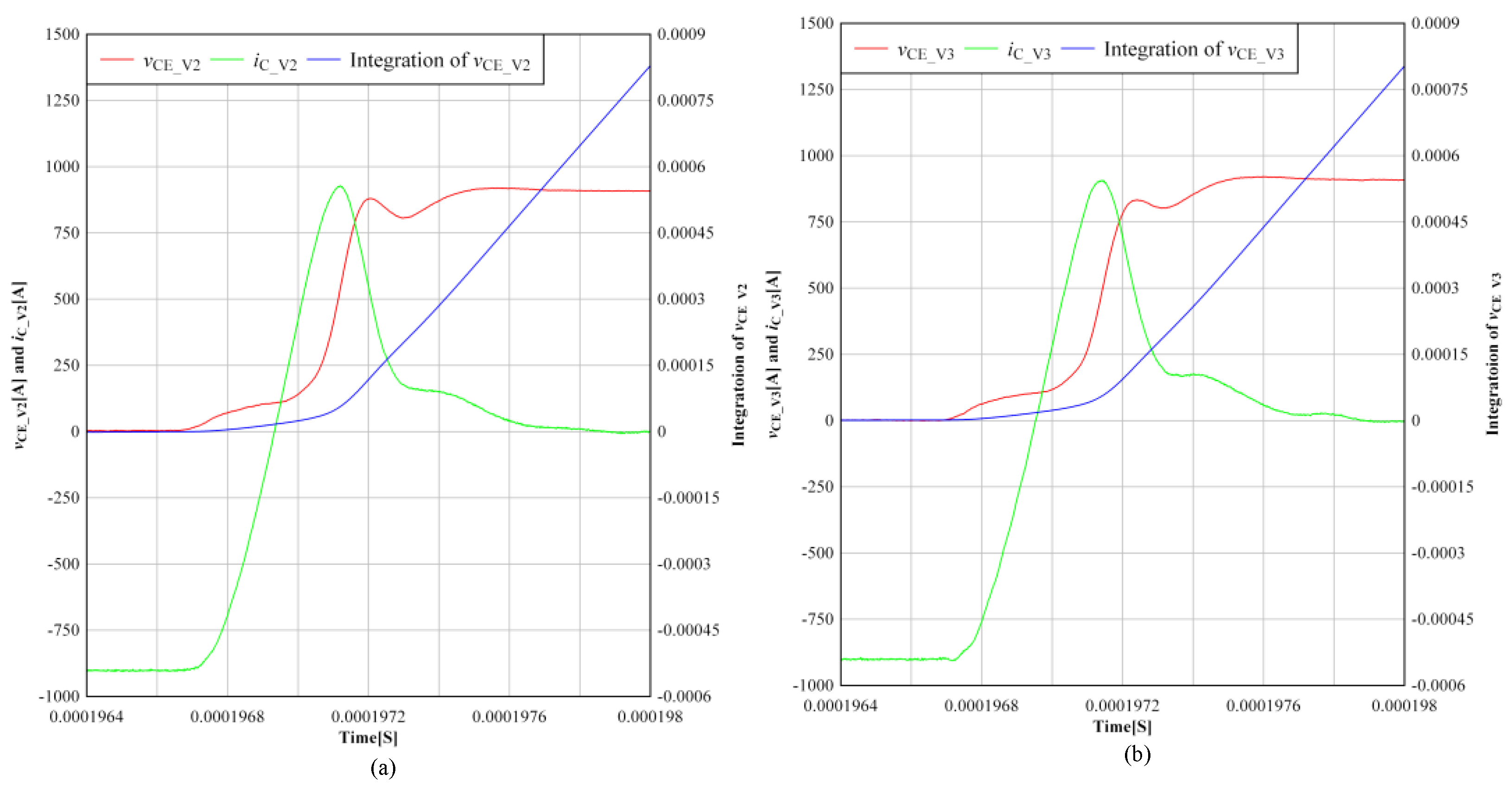
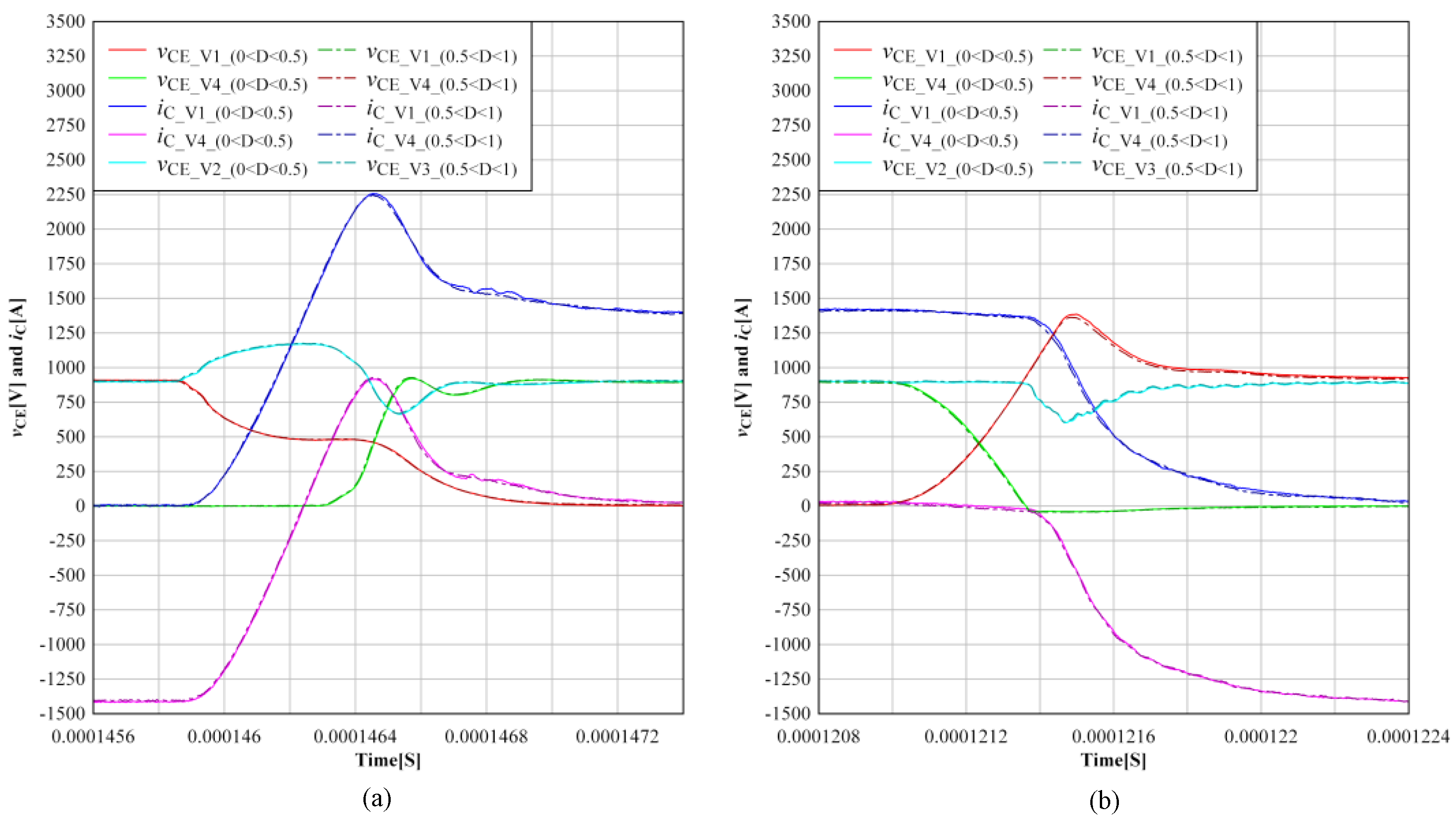
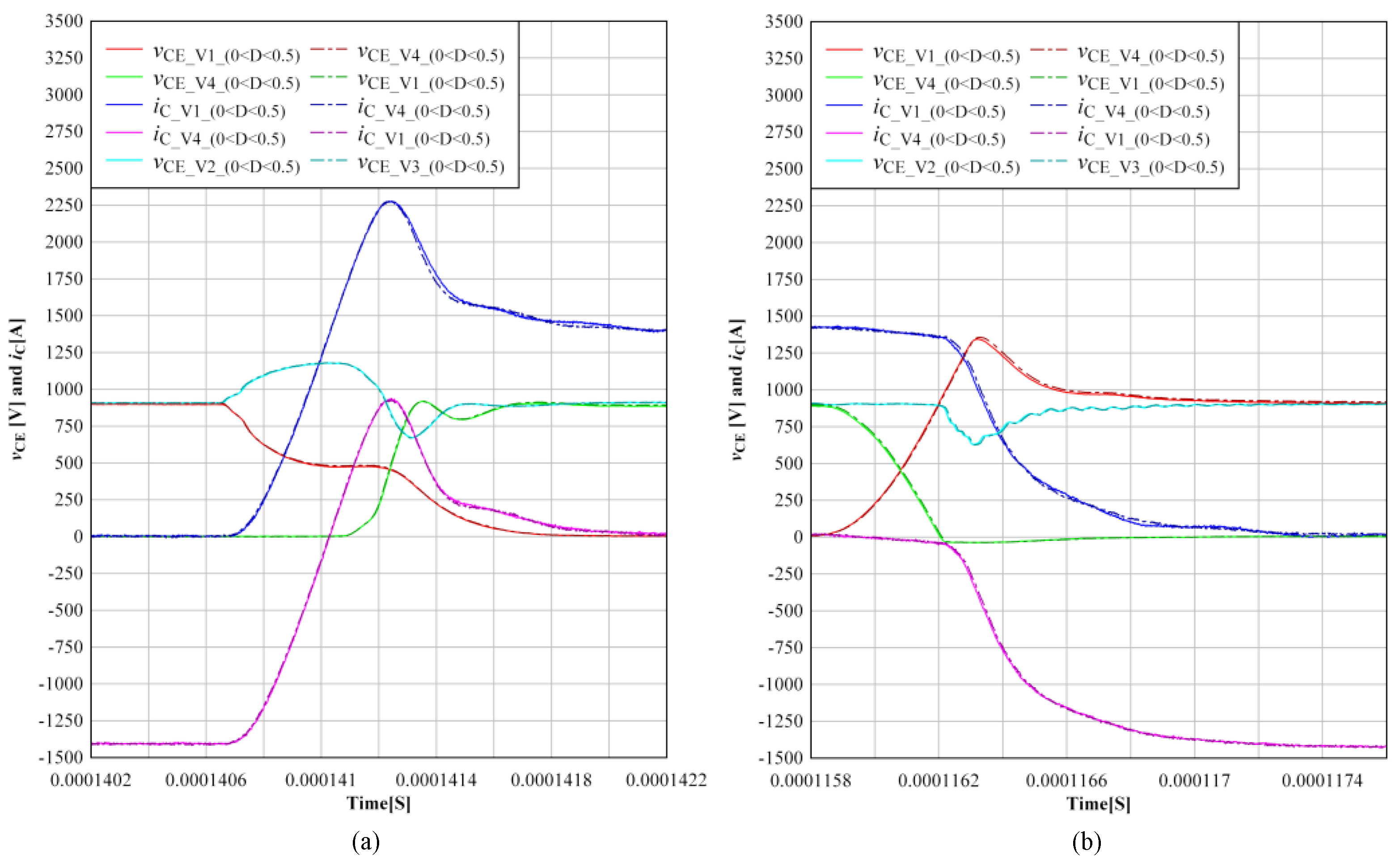
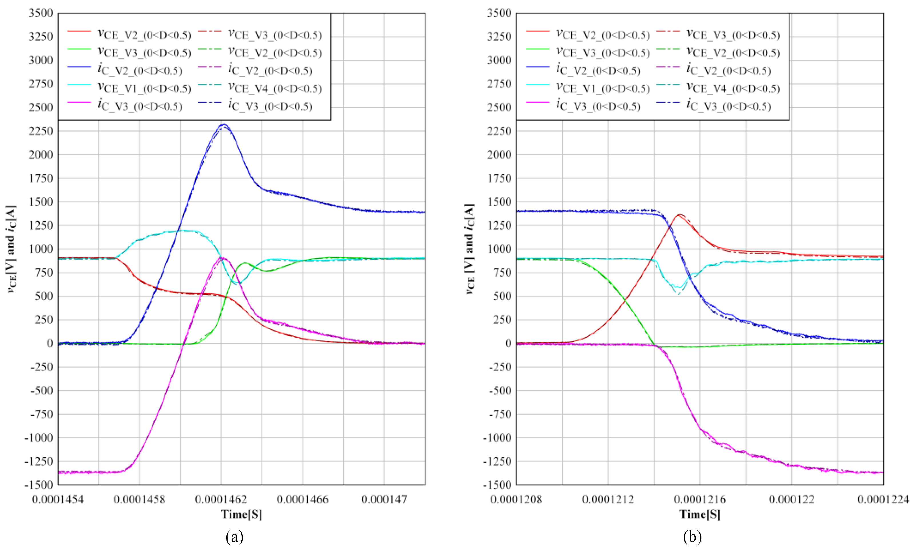
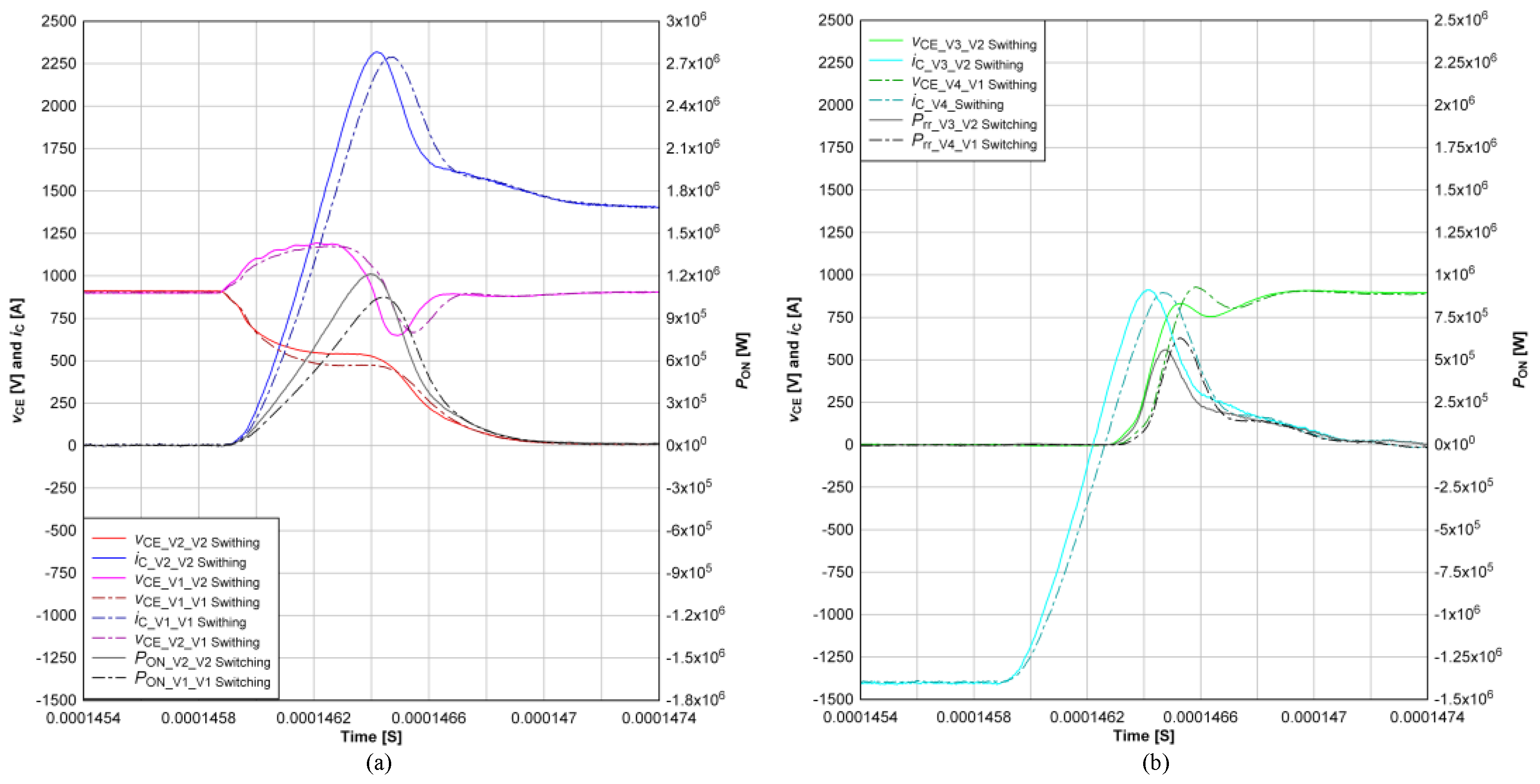
6.3. The Influence of Current Paths on IGBT Switching Characteristics

Double-pulse tests were performed under DC-Link voltages of 1.8 kV and 0.9 kV for the flying capacitor with a 1.4 kA inductive load in buck mode. The definition of IGBT turn-on energy (Eon), IGBT turn-off energy (Eoff), and FWD reverse recovery energy (Err) are referred to in [35,36]. VCE, VR, iC, and iF were sampled and recorded by a digital oscilloscope. Voltages were measured by differential voltage probes (THDP0100 from TEK [37]), with a DC to 100 MHz bandwidth and maximum measurable differential voltage of 6 kV. Currents were measured by a CWT30B Rogowski coil from PEM [38], with a 0.5 Hz to 100 MHz bandwidth and maximum measurable current of 6 kA.
For the FC-3L-BDC phase-leg PEBB, the switching process of the outer loop and the inner loop for different duty cycles (0 < D < 0.5 and 0.5 < D < 1) of active switches were compared in buck mode. The waveforms are shown in Figure 19 and Figure 20, and the parameters are listed in Table 7. It is clear that IGBT switching characteristics are identical for 0 < D < 0.5 and 0.5 < D < 1 in buck mode. Similarly, the result can be obtained in boost mode.

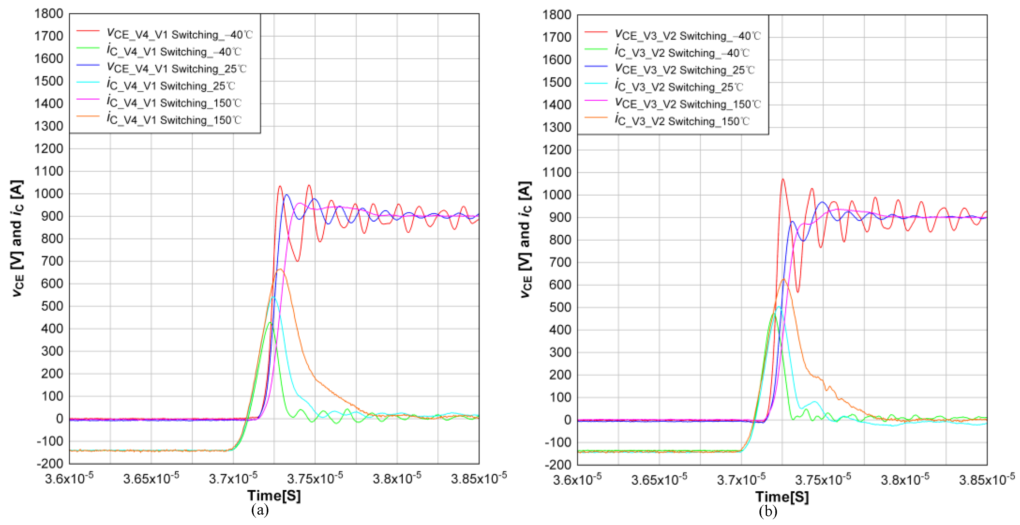
6.4. The Influence of IGBT Position on IGBT Switching Characteristics

According to the analysis in Section 3, the current path in buck mode with 0 < D < 0.5 is the same as that in boost mode with 0.5 < D < 1, and the current path in buck mode with 0.5 < D < 1 is the same with that in boost mode with 0 < D < 0.5, while the active switches and freewheeling diodes are in the opposite position. In this section, for both the inner loop and outer loop, the switching process in buck mode with 0 < D < 0.5 and boost mode with 0.5 < D < 1 are compared. The waveforms are shown in Figure 21 and Figure 22, and the parameters are listed in Table 8. It is clear that the switching characteristics of IGBTs and FWDs are not influenced by the position of active switches.

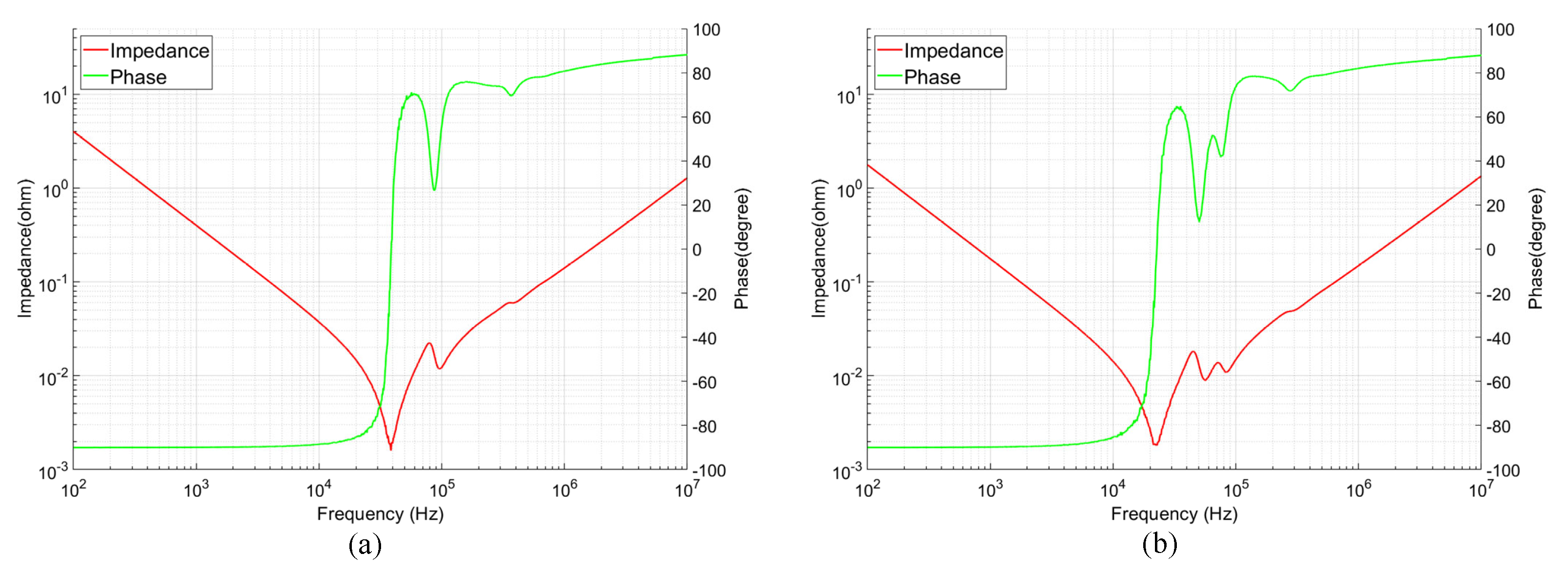
6.5. Stray Inductance Measurements

During IGBT turn-on, the voltage drop between the collector and emitter is only determined by commutation path Lσ, so Lσ can be extracted by measuring the voltage drop of the stray inductance and the value of diF/dt at the moment of the forward current cross zero. FC-3L-BDC has four working modes with eight different kinds of current paths, but there are only two commutation loops. The comparison analyses of switching characteristics in different current paths and working modes verified that the switching characteristics of IGBTs are not influenced by the current paths and the positions of active switches. Consequently, the stray inductance can be extracted in any working mode, and in this paper, the buck mode with 0 < D < 0.5 was selected, as shown in Figure 23. Equations (15) and (16) show the extraction method of Lσ for the inner and outer commutation paths.
L σ _ I = t 0 t 0 + Δ t ( V D C _ F C V C E _ V 2 V C E _ V 3 ) d t i c _ V 3 ( t 0 + Δ t ) i c _ _ V 3 ( t 0 ) = 3.1191 × 10 5 1.17 ( 507.42 ) = 61.33 n H ,
L σ _ O = t 0 t 0 + Δ t ( V D C _ l i n k V D C _ F C V C E _ V 1 V C E _ V 4 ) d t i c _ V 4 ( t 0 + Δ t ) i c _ _ V 4 ( t 0 ) = 3.9813 × 10 5 [ 8.28 ( 508.13 ) ] = 79.65 n H ,
The measured value of Lσ for the outer and inner commutation paths is less than the estimated values in Section 5, but the deviation is around 0.6% for the inner loop and 0.4% for the outer loop. The results demonstrate that the 3D-FEA is an effective method for bus bar stray inductance extraction. For the FC-3L-BDC application, the stray inductance of the IGBT device and capacitor should be remeasured instead of directly adopting the value given by datasheets.

6.6. Comparison of Outer and Inner Commutation Paths

In this section, the outer and inner commutation paths of the phase-leg of FC-3L-BDC are compared during IGBT turn-off and turn-on in buck mode with D < 0.5, as shown in Figure 24 and Figure 25. The tests were performed with 1.8 kV for the high-voltage side, 0.9 kV for the flying capacitor, and 1.4 kA for the inductive load.
As shown in Figure 24a and Figure 25a, in the condition above, for this PEBB, the turn-off overvoltage of the active switch and coupling overvoltage of the other switch caused by the intercoupling of the inner and outer commutation paths are less than 1.7 kV. The overvoltage and peak power of IGBT turn-off of the outer commutation path is almost the same as those of the inner commutation path. The peak power of IGBT turn-on of the outer commutation path is around 14% smaller than that of the inner commutation path. The peak power of FWD reverse recovery of the outer commutation path is 12% higher than that of the inner commutation path.
The double-pulse test at −40 °C and +150 °C of Tvj shows that 1.8 kV for the high-voltage side and 0.9 kV for the flying capacitor are safe operating voltages for the PEBB.

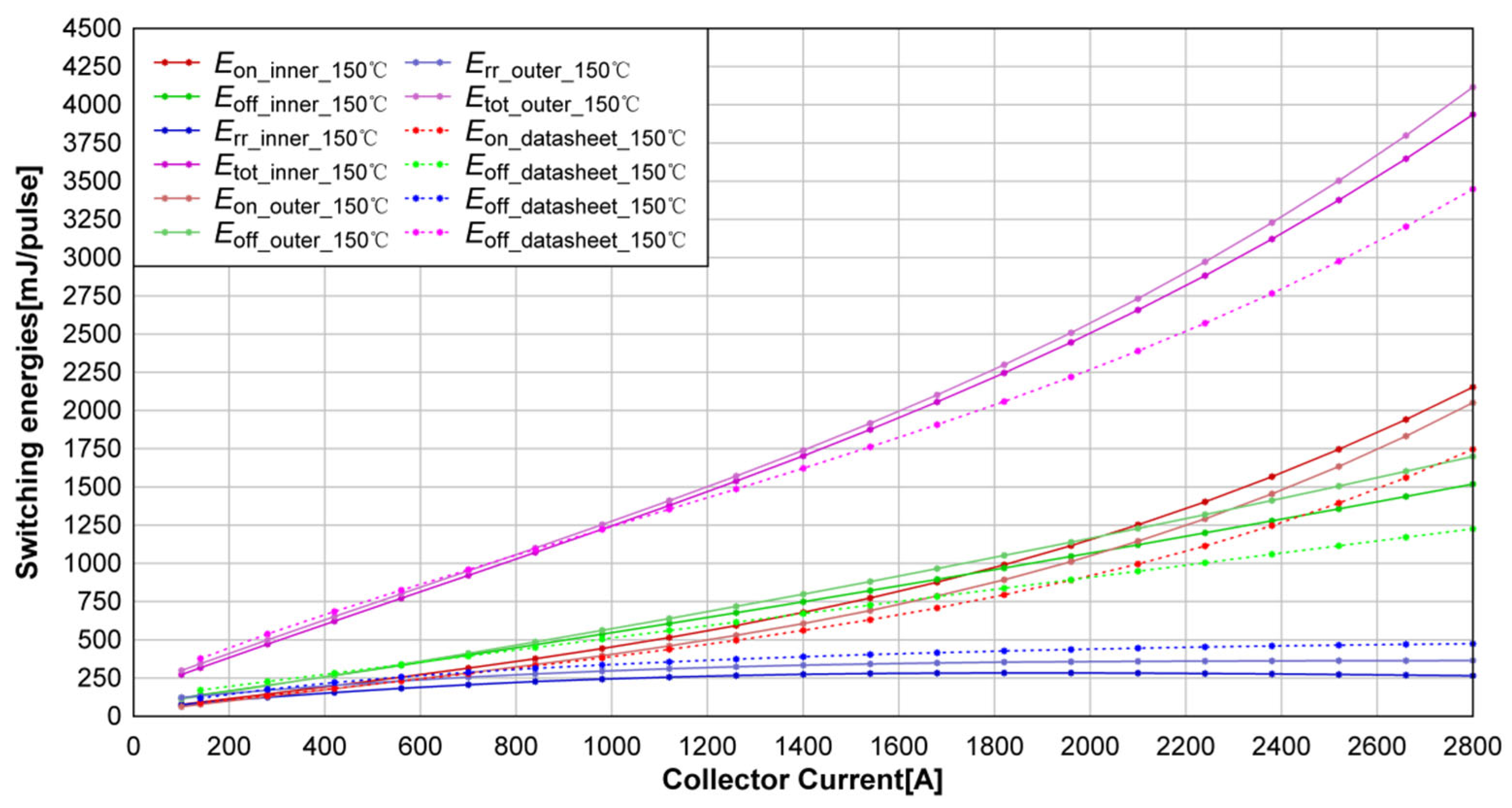
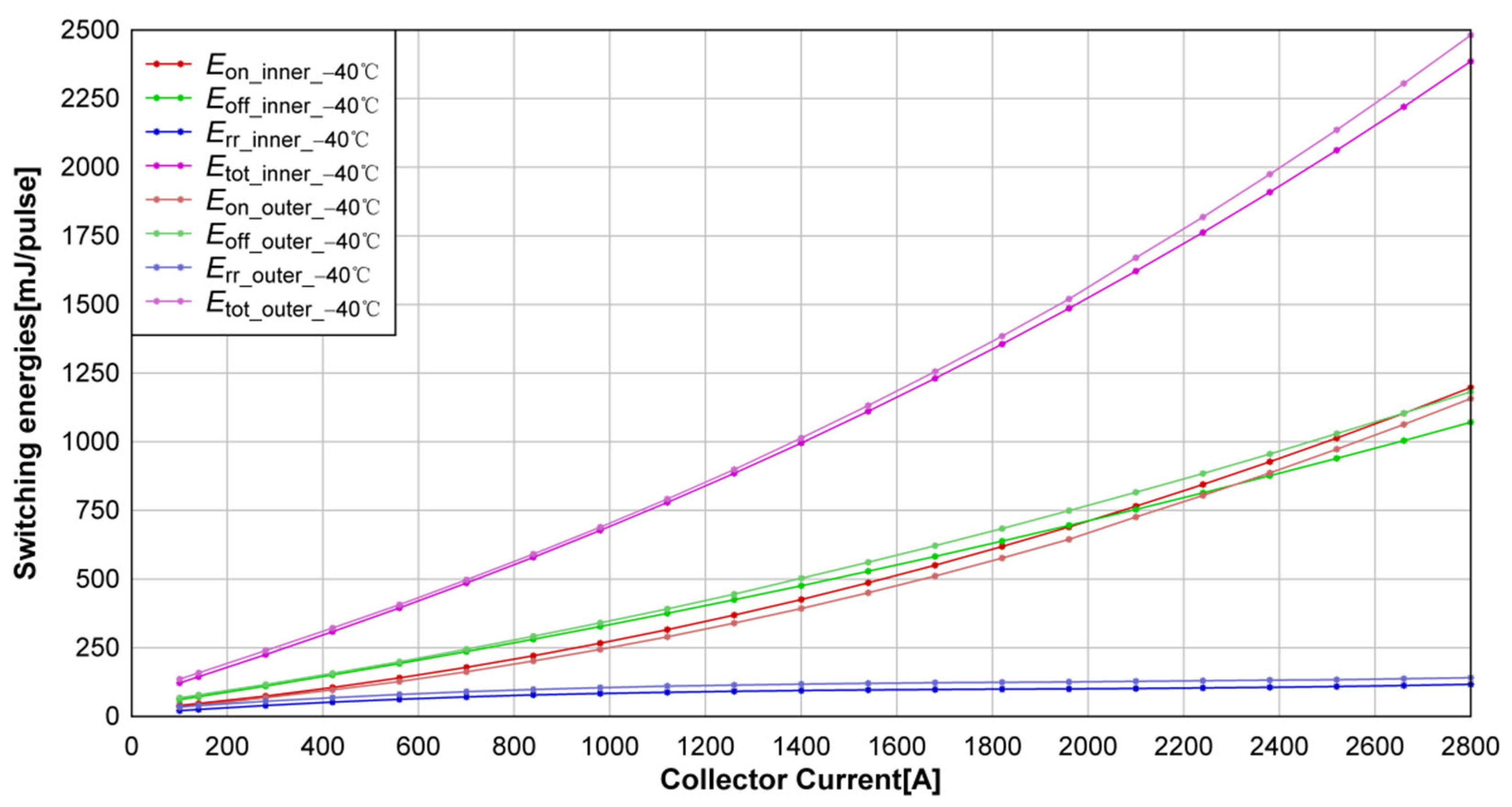
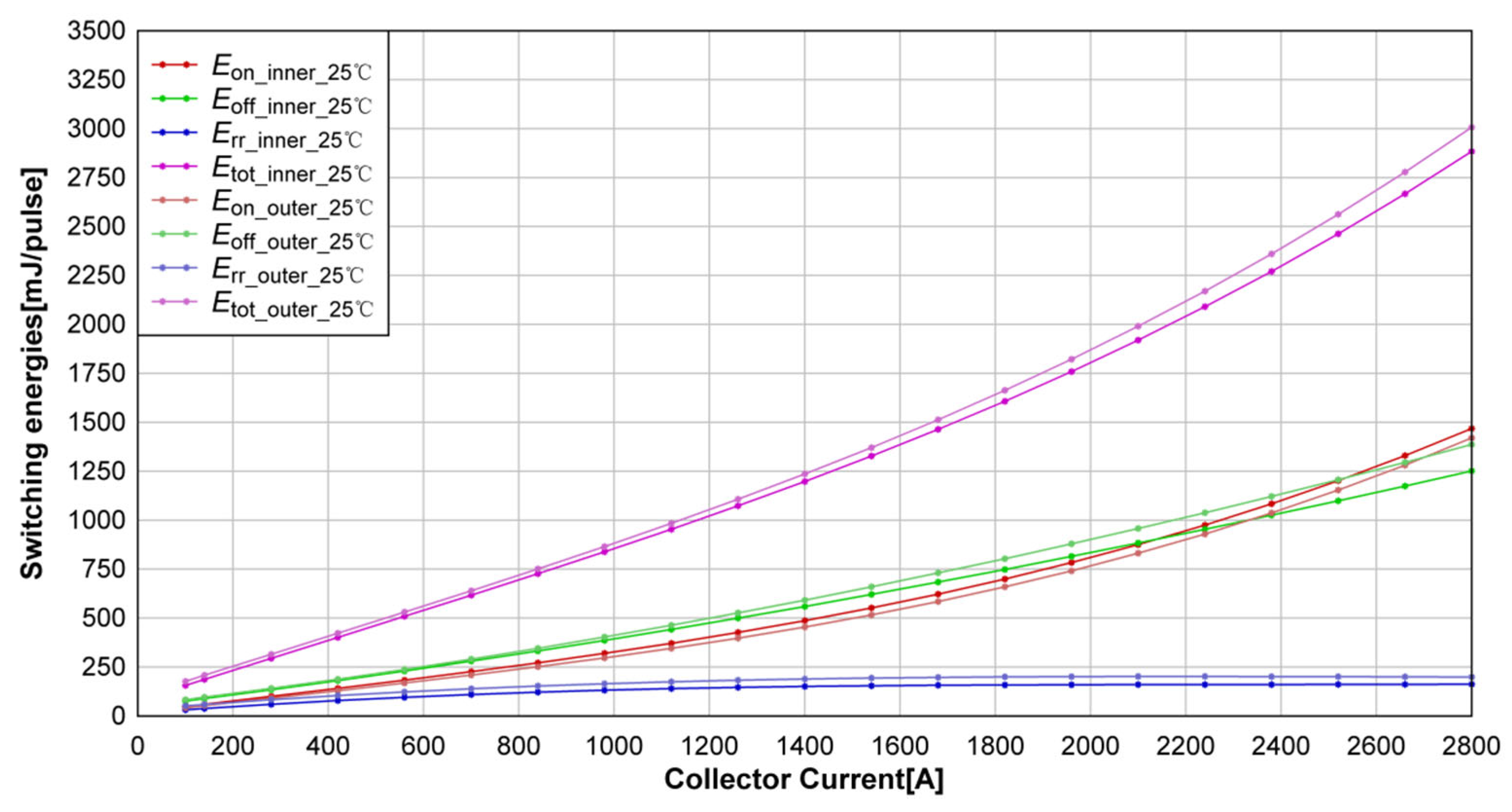
6.7. Switching Energy Loss Measurements

The switching energies of the PEBB at −40 °C and 25 °C with 1.8 kV for the high-voltage side and 0.9 kV for the flying capacitor in buck mode with 0 < D < 0.5 are shown in Figure 26 and Figure 27. The switching energies given by the datasheet and the test results of the PEBB at 150 °C are shown in Figure 28. For the outer commutation path, Eon and Eoff dissipate in V1, and Err dissipates in V4. For the inner commutation path, Eon and Eoff dissipate in V2, and Err dissipates in V3. The switching energies are calculated based on the data from double-pulse tests as in [35,36].
One of the main issues in designing the PEBB is ensuring that the power losses in each working mode are balanced. The total power losses consist of conduction losses and switching losses. The conduction losses are determined by the output characteristic of IGBT and forward characteristic of FWD, and the switching losses are determined by the switching losses of IGBT and FWD. All of the IGBT devices of the PEBB are the same, so the conduction losses are identical for the inner and outer commutation paths, although Eoff, Eon, and Err are affected by Lσ of commutation paths. As shown in Figure 26, Figure 27 and Figure 28, Etot remains almost stable against Lσ variations, and Etot of the outer commutation path is approximately 3% higher than that of the inner commutation path.
The switching losses extracted by the double-pulse test confirmed the anticipations that Eoff and Err would increase and Eon would decrease with the increasing of Lσ of the commutation path. Moreover, the prediction that the switching losses would increase with the junction temperature increasing was exactly confirmed.
The switching losses given by the datasheet are measured for a certain Lσ value of the commutation path, normally around 30nH for the PrimePACK3 IGBT devices. As shown in Figure 28, if the switching losses given by the datasheet are directly used, an underestimated value is obtained in terms of IGBT power losses.

6.8. Verification of Snappy Reverse Recovery in the FWD

As shown in Figure 29, the reverse recovery of FWD was tested with a 1.8 kV high-voltage side, 0.9 kV flying capacitor voltage, and one-tenth of the nominal IGBT collector current, 140 A, for the outer and inner commutation paths of the PEBB.
Inconspicuous strong snappy reverse recovery behavior or voltage spike were detected over any FWD in FF1400R17IP4 of the FC-3L-BDC phase-leg PEBB. As shown in Figure 29, it is demonstrated that a higher commutation path Lσ would induce higher reverse recovery voltage spikes over the corresponding FWD inside IGBT devices. Concerning the reverse recovery behavior of the FWD, enough margins have been confirmed by a double-pulse test within the entire current range of the IGBT device in the condition of 1.8 kV of high-voltage side, 0.9 kV of flying capacitor voltage at −40 °C, 25 °C and +150 °C of Tvj.

7. Conclusions

This paper presents for the first time the design of a high-power FC-3L-BDC phase-leg PEBB from the aspects of commutation path analysis, IGBT device selection, insulation-strengthening design, low-stray-inductance bus bar design, and commutation behavior analysis. This paper proposes a stray inductance matrix simulation method for bus bars based on 3D-FEA, a stray inductance test method for IGBT devices adapted to three-level applications, and a more accurate stray inductance test method for capacitors. Using the stray inductance test method proposed in this paper, the error between the estimated stray inductance and the measured stray inductance of commutation loop is less than 1%. The stray inductance analysis method proposed in this paper can be applied to PEBB stray inductance analysis of other topologies.
Based on the FC-3L-BDC phase-leg PEBB designed in this paper, it is experimentally verified that the switching characteristics of IGBT devices are determined only by the stray inductance of the commutation path and not affected by the current path or the position of the active IGBT device. The PEBB has extremely low commutation stray inductance, which enables snubberless operation. The total switching loss difference between the inner- and outer-loop IGBT devices is less than 3%, which facilitates the construction of BDC with a stable output capability under different working modes. Neither the excessive turn-off overvoltage of IGBTs nor the snappy reverse recovery of FWDs was observed. The PEBB of FC-3L-BDC designed in this paper can meet the requirements of building 400kW to MW bidirectional DC-DC converters for light rail chargers, metro regenerative braking energy recovery, and energy storage in the DC microgrid.

Author Contributions

Conceptualization, H.L. and Z.D.; methodology, H.L., Z.D., Y.Q. and S.X.; software, H.L., F.L. and Y.T.; validation, Z.D., Y.Q. and S.X.; formal analysis, Z.D., Y.Q., and S.X.; investigation, S.X., F.L. and Y.T.; resources, H.L. and Z.D.; data curation, S.X., F.L. and Y.T.; writing—original draft preparation, S.X., F.L. and Y.T.; writing—review and editing, H.L., Z.D., Y.Q. and S.X.; visualization, S.X.; supervision, Y.Q.; project administration, Z.D. All authors have read and agreed to the published version of the manuscript.

Funding

This research received no funding.

Data Availability Statement

The data presented in this study are available on request from the corresponding author. The data are not publicly available due to corporate intellectual property management requirements.

Conflicts of Interest

The authors declare no conflict of interest. The funders had no role in the design of the study; in the collection, analyses, or interpretation of data; in the writing of the manuscript; or in the decision to publish the results.

References

  1. IPCC. 2021: Summary for Policymakers. In Climate Change 2021: The Physical Science Basis. Contribution of Working Group I to the Sixth Assessment Report of the Intergovernmental Panel on Climate Change; Masson-Delmotte, V., Zhai, P., Pirani, A., Connors, S.L., Péan, C., Berger, S., Caud, N., Chen, Y., Goldfarb, L., Gomis, M.I., Eds.; Cambridge University Press: Cambridge, UK; New York, NY, USA, 2021; pp. 3–32. [Google Scholar] [CrossRef]
  2. IPCC. 2022: Summary for Policymakers. In Climate Change 2022: Mitigation of Climate Change. Contribution of Working Group III to the Sixth Assessment Report of the Intergovernmental Panel on Climate Change; Shukla, P.R., Skea, J., Slade, R., Al Khourdajie, A., van Diemen, R., McCollum, D., Pathak, M., Some, S., Vyas, P., Fradera, R., Eds.; Cambridge University Press: Cambridge, UK; New York, NY, USA, 2021. [Google Scholar] [CrossRef]
  3. Bi, K.; Lv, H.; Chen, L.; Li, J.; Zhu, Y.; Huang, W.; Fan, Q. A Model Predictive Controlled Bidirectional Four Quadrant Flying Capacitor DC/DC Converter Applied in Energy Storage System. IEEE Trans. Power Electron. 2022, 37, 7705–7717. [Google Scholar] [CrossRef]
  4. Yagoub, M.A.; Tao, Z. Modelling analysis and simulation of a micro-grid using photovoltaic (PV) & battery based power generation. In Proceedings of the 16th IET International Conference on AC and DC Power Transmission (ACDC 2020), Online, 2–3 July 2020; pp. 1514–1521. [Google Scholar] [CrossRef]
  5. Jayan, V.; Ghias, A.M.Y.M. A Single-Objective Modulated Model Predictive Control for a Multilevel Flying Capacitor Converter in a DC Microgrid. IEEE Trans. Power Electron. 2022, 37, 1560–1569. [Google Scholar] [CrossRef]
  6. Jin, K.; Ruan, X.; Yang, M.; Xu, M. A Hybrid Fuel Cell Power System. IEEE Trans. Ind. Electron. 2008, 56, 1212–1222. [Google Scholar] [CrossRef]
  7. Hasimi, N.; Hinz, H.; Schofield, N. Comparative Analysis of Bidirectional DC-DC Converters for Fuel Cell Hybrid Vehicles. In Proceedings of the 10th International Conference on Power Electronics, Machines and Drives (PEMD 2020), Online, 15–17 December 2020; pp. 68–74. [Google Scholar] [CrossRef]
  8. Qu, X.; Tian, L.; Li, J.; Lou, C.; Jiang, T. Research on Charging and discharging Strategies of Regenerative Braking Energy Recovery System for Metro Flywheel. In Proceedings of the 2021 3rd Asia Energy and Electrical Engineering Symposium (AEEES), Chengdu, China, 26–29 March 2021; pp. 1087–1095. [Google Scholar] [CrossRef]
  9. Lu, Y.; Zhao, Y.; Zhao, X.; Li, G.; Zhang, C. Status analysis of regenerative braking energy utilization equipments in urban rail transit. In Proceedings of the 2017 IEEE Transportation Electrification Conference and Expo, Asia-Pacific (ITEC Asia-Pacific), Harbin, China, 7–10 August 2017; pp. 1–6. [Google Scholar] [CrossRef]
  10. Chen, L.; Huang, K.; Lv, W.; Zhang, D.; Huang, S. Control Strategy of Modularized Ultra-capacitor Energy Storage System for Regenerative Braking Energy in Metro-Transit Systems. In Proceedings of the 2019 22nd International Conference on Electrical Machines and Systems (ICEMS), Harbin, China, 11–14 August 2019; pp. 1–5. [Google Scholar] [CrossRef]
  11. Calderaro, V.; Galdi, V.; Graber, G.; Piccolo, A. Siting and sizing of stationary Super Capacitors in a Metro Network. In Proceedings of the AEIT Annual Conference 2013 (AEIT), Mondello, Palermo, Italy, 3–5 October 2013; pp. 1–5. [Google Scholar] [CrossRef]
  12. Flynn, M.; Mcmullen, P.; Solis, O. Saving energy using flywheels. IEEE Ind. Appl. Mag. 2008, 14, 69–76. [Google Scholar] [CrossRef]
  13. Liang, H.; Dong, L.; Hu, J.; Chen, Y. Energy Management Strategy Based on Dynamic Threshold for Energy Recovery System in Rail Transit. In Proceedings of the 2019 IEEE Vehicle Power and Propulsion Conference (VPPC), Hanoi, Vietnam, 14–17 October 2019; pp. 1–6. [Google Scholar] [CrossRef]
  14. Bhanderi, M.D.; Chavda, J.K. Ultra-capacitor based three level bi-directional isolated DC-DC converter for the regenerative breaking energy recovery system. In Proceedings of the 2017 International Conference on Information, Communication, Instrumentation and Control (ICICIC), Indore, India, 17–19 August 2017; pp. 1–6. [Google Scholar] [CrossRef]
  15. Grbovic, P.J.; Delarue, P.; Le Moigne, P. Interface converters for ultra-capacitor applications in power conversion systems. In Proceedings of the 2012 15th International Power Electronics and Motion Control Conference (EPE/PEMC), Novi Sad, Serbia, 4–6 September 2012; pp. LS7d.1-1–LS7d.1-7. [Google Scholar] [CrossRef]
  16. Ruan, X.; Wei, J.; Xue, Y. Three-level converters with the input and output sharing the ground. In Proceedings of the IEEE 34th Annual Conference on Power Electronics Specialist, 2003. PESC ‘03, Acapulco, Mexico, 15–19 June 2003; Volume 4, pp. 1919–1923. [Google Scholar] [CrossRef]
  17. Jin, K.; Yang, M.; Ruan, X. Three-Level Bi-Directional Converter—A Novel DC-DC Converter Suitable for Fuel Cell Power System. In Proceedings of the 2006 37th IEEE Power Electronics Specialists Conference, Jeju, Korea, 18–22 June 2006; pp. 1–6. [Google Scholar] [CrossRef]
  18. Chen, H.-C.; Lu, C.-Y.; Lien, W.-H. Active capacitor voltage balancing control for three-level flying capacitor boost converter. In Proceedings of the 2018 IEEE Applied Power Electronics Conference and Exposition (APEC), San Antonio, TX, USA, 4–8 March 2018; pp. 127–132. [Google Scholar] [CrossRef]
  19. Kan, Z.; Li, P.; Yuan, R.; Zhang, C. Interleaved three-level bi-directional DC-DC converter and power flow control. In Proceedings of the 2018 3rd International Conference on Intelligent Green Building and Smart Grid (IGBSG), Yilan, Taiwan, 22–25 April 2018; pp. 1–4. [Google Scholar] [CrossRef]
  20. Zhang, D.; Chen, C.; Ou, Y.; Zheng, T.; Tang, W. Model predictive control of three-level bidirectional DC-DC converter based on super capacitor energy storage system. In Proceedings of the 2020 International Conference on Electrical Engineering (ICEE), Bandung, Indonesia, 23–24 September 2020; pp. 1–5. [Google Scholar] [CrossRef]
  21. Mahmoudi, M.A.H.; Ahmadi, R. Modulated model predictive control of three level flying capacitor buck converter. In Proceedings of the 2017 IEEE Power and Energy Conference at Illinois (PECI), Champaign, IL, USA, 23–24 February 2017; pp. 1–5. [Google Scholar] [CrossRef]
  22. Putera, P.; Klumpner, C.; Wheeler, P. A bidirectional three-level interleaved DC-DC converter for an electric vehicle charging station operating in a wide range of battery currents and voltages. In Proceedings of the 11th International Conference on Power Electronics, Machines and Drives (PEMD 2022), Newcastle, UK, 21–23 June 2022; pp. 439–445. [Google Scholar] [CrossRef]
  23. Ying, Z.; Liang, Z.; Weichao, L.; Xiangming, Z.; Bing, L. Commutation behaviour analysis of a 3L-ANPC-VSC phase-leg PEBB using 4.5kV and 3kA press-pack IGBT. In Proceedings of the 16th IET International Conference on AC and DC Power Transmission (ACDC 2020), Online, 2–3 July 2020; pp. 1837–1842. [Google Scholar] [CrossRef]
  24. Volke, A.; Hornkamp, M. IGBT Modules; Technologies, Driver and Application; Infineon Technol. AG: Neubiberg, Germany, 2012. [Google Scholar]
  25. Wintrich, A.; Nicolai, U.; Tursky, W.; Reimann, T. Application Manual Power Semiconductors; Semikron Int. GmbH: Nuremberg, Germany, 2015. [Google Scholar]
  26. Jin, K.; Yang, M.; Ruan, X.; Xu, M. Three-Level Bidirectional Converter for Fuel-Cell/Battery Hybrid Power System. IEEE Trans. Ind. Electron. 2009, 57, 1976–1986. [Google Scholar] [CrossRef]
  27. Infineon. Properties of a New PrimePACK™ IGBT Module Concept for Optimized Electrical and Thermal Interconnection to a Modern Converter Environment. 2015. Available online: https://www.infineon.com/dgdl/Infineon-PCIM_2005_Properties_of_a_New_PrimePACK-ED-v1.0-en.pdf?fileId=db3a304412b407950112b40edb6112a9&da=t (accessed on 18 April 2022).
  28. IEC 61287-1:2014; Railway Applications—Power Converters Installed on Board Rolling Stock—Part 1: Characteristics and Test Methods. International Electrotechnical Commission: Geneva, Switzerland, 2014.
  29. Mayor, A.; Rizo, M.; Monter, A.R.; Bueno, E.J. Commutation Behavior Analysis of a Dual 3L-ANPC-VSC Phase-Leg PEBB Using 4.5-kV and 1.5-kA HV-IGBT Modules. IEEE Trans. Power Electron. 2018, 34, 1125–1141. [Google Scholar] [CrossRef]
  30. Skibinski, G.L.; Divan, D.M. Design methodology and modeling of low inductance planar bus structures. In Proceedings of the 1993 Fifth European Conference on Power Electronics and Applications, Brighton, UK, 13–16 September 1993; Volume 3, pp. 98–105. [Google Scholar]
  31. IEC 62497-1:2010+AMD1:2013; Railway Applications—Insulation Coordination—Part 1: Basic Requirements—Clearances and Creepage Distances for All Electrical and Electronic Equipment. International Electrotechnical Commission: Geneva, Switzerland, 2013.
  32. Engelmann, G.; Quabeck, S.; Gottschlich, J.; De Doncker, R.W. Experimental and simulative investigations on stray capacitances and stray inductances of power modules. In Proceedings of the 2017 19th European Conference on Power Electronics and Applications (EPE’17 ECCE Europe), Warsaw, Poland, 11–14 September 2017; pp. P.1–P.10. [Google Scholar] [CrossRef]
  33. IEC 61071:2017; Capacitors for Power Electronics. International Electrotechnical Commission: Geneva, Switzerland, 2017.
  34. KEYSIGHT. Impedance Measurement Handbook. 2016. Available online: https://www.keysight.com/us/en/assets/7018-06840/application-notes/5950-3000.pdf (accessed on 18 April 2022).
  35. IEC 60747-2:2016; Semiconductor Devices—Part 2: Discrete Devices—Rectifier Diodes. International Electrotechnical Commission: Geneva, Switzerland, 2016.
  36. IEC 60747-9:2019; Semiconductor Devices—Part 9: Discrete Devices—Insulated-Gate Bipolar Transistors (IGBTs). International Electrotechnical Commission: Geneva, Switzerland, 2019.
  37. Tektronix. THDP0100/0200 & TMDP0200 High Voltage Differential Probes Instruction Manual. Available online: https://download.tek.com/manual/THDP0100-0200-TMDP0200-High-Voltage-Differential-Probe-Instruction-Manual-ZH-CN-077054301.pdf (accessed on 18 April 2022).
  38. PEM. Available online: http://www.pemuk.com/Userfiles/CWT/cwt_0318.pdf (accessed on 18 April 2022).
Figure 1. The topological structure of FC-3L-BDC.
Energies 15 09651 g001
Figure 2. Key waveforms. (a) Boost mode (0.5 < D < 1) and buck mode (0 < D < 0.5). (b) Boost mode (0 < D < 0.5) and buck mode (0.5 < D < 1).
Energies 15 09651 g002
Figure 3. Commutation paths of FC-3L-BDC. (a) Buck mode, D < 0.5 (V1 switching). (b) Buck mode, D < 0.5 (V2 switching).
Energies 15 09651 g003
Figure 4. Commutation paths of FC-3L-BDC. (a) Buck mode, 0.5 < D < 1 (V1 switching). (b) Buck mode, 0.5 < D < 1 (V2 switching).
Energies 15 09651 g004
Figure 5. Commutation paths of FC-3L-BDC. (a) Boost mode, D < 0.5 (V4 switching). (b) Boost mode, D < 0.5 (V3 switching).
Energies 15 09651 g005
Figure 6. Commutation paths of FC-3L-BDC. (a) Boost mode, 0.5 < D < 1 (V4 switching). (b) Boost mode, 0.5 < D < 1 (V3 switching).
Energies 15 09651 g006
Figure 7. External appearance of the series of PrimePACK of Infineon. (a) PrimePACK 2. (b) PrimePACK 3. (c) PrimePACK 3+.
Energies 15 09651 g007
Figure 8. Three FC-3L-BDC phase-leg PEBBs and DC_link capacitors. (a) Three-dimensional models. (b) Simplified electrical scheme of single FC-3L-BDC phase-leg PEBB.
Energies 15 09651 g008
Figure 9. The physical placement of IGBT devices and polarity assignment of bus bar for the PEBB of FC-3L-BDC.
Energies 15 09651 g009
Figure 10. A lumped stray inductance model of inner and outer commutation paths for the PEBB of FC-3L-BDC.
Energies 15 09651 g010
Figure 11. The chips layout and power terminal structure of PrimePACK3.
Energies 15 09651 g011
Figure 12. Schematic of stray inductance measurement for IGBT devices. (a) Upper switch stray-inductance-measuring circuit. (b) Typical test waveforms.
Energies 15 09651 g012
Figure 13. Stray inductance measurements of the upper and lower switches for FF1400R17IP4. (a) The lower switch test waveforms. (b) The upper switch test waveforms.
Energies 15 09651 g013
Figure 14. Stray inductance measurements of the DC-link capacitor and flying capacitor. (a) The flying capacitor test waveforms. (b) The DC-link capacitor test waveforms.
Energies 15 09651 g014
Figure 15. Impedance analysis of the DC-link and flying capacitor. (a) The flying capacitor. (b) The DC-ink capacitor.
Energies 15 09651 g015
Figure 16. Photograph of the test bench.
Energies 15 09651 g016
Figure 17. A Simplified schematic of the double-pulse test bench for the FC-3L-BDC phase-leg PEBB in buck mode.
Energies 15 09651 g017
Figure 18. The sequence of double-pulse test.
Energies 15 09651 g018
Figure 19. Influence of the current paths of outer commutation loop in buck mode. (a) Detail waveforms during IGBT turn-on. (b) Detail waveforms during IGBT turn-off.
Energies 15 09651 g019
Figure 20. Influence of the current paths of inner commutation loop in buck mode. (a) Detail waveforms during IGBT turn-on. (b) Detail waveforms during IGBT turn-off.
Energies 15 09651 g020
Figure 21. Influence of active switch position of outer commutation loop. (a) Detail waveforms of IGBT and FWD during IGBT turn-on. (b) Detail waveforms of IGBT and FWD during IGBT turn-off.
Energies 15 09651 g021
Figure 22. Influence of active switch position of inner commutation loop. (a) Detail waveforms of IGBT and FWD during IGBT turn-on. (b) Detail waveforms of IGBT and FWD during IGBT turn-off.
Energies 15 09651 g022
Figure 23. Stray inductance measurements of the PEBB of FC-3L-BDC. (a) The measurement of the outer commutation path. (b) The measurement of the inner commutation path.
Energies 15 09651 g023
Figure 24. Influence of the stray inductance during IGBT turn-off at 0.9 kV and 1.4 kA (Tvj = 25 °C, VGEoff =−15 V, and RGoff = 1.57 Ω). (a) Detail waveforms through IGBT. (b) Detail waveforms through FWD.
Energies 15 09651 g024
Figure 25. Influence of the stray inductance during IGBT turn-on at 0.9 kV and 1.4 kA (Tvj = 25 °C, VGEon = −15 V, and RGon = 0.9 Ω). (a) Detail waveforms through IGBT. (b) Detail waveforms through FWD.
Energies 15 09651 g025
Figure 26. IGBT switching energies between the inner and the outer commutation paths at −40 °C.
Energies 15 09651 g026
Figure 27. IGBT switching energies between the inner and the outer commutation paths at 25 °C.
Energies 15 09651 g027
Figure 28. IGBT switching energies between the inner commutation path, the outer commutation path, and data given by datasheet at 150 °C.
Energies 15 09651 g028
Figure 29. FF1400R17IP4 reverse recovery with 0.9 kV off voltage and 140 A (Tvj = −40 °C, 25 °C, and 150 °C, VGEon = +15 V, RGon = 0.9 Ω). (a) The outer commutation path. (b) The inner commutation path.
Energies 15 09651 g029
Table 1. The working modes of FC-3L-BDC.
Energy Transmit DirectionRelationship of High-Voltage Side and Low-Voltage SideWorking Mode
High-Voltage Side to Low-Voltage SideVL < VH/2Buck, 0 < D < 0.5
High-Voltage Side to Low-Voltage SideVL > VH/2Buck, 0.5 < D < 1
Low-Voltage Side to High-Voltage SideVL < VH/2Boost, 0.5 < D < 1
Low-Voltage Side to High-Voltage SideVL > VH/2Boost, 0 < D < 0.5
Table 2. The switch statuses and commutation paths of different working modes.
Working ModeActive IGBTReverse Recovery FWDCommutation Paths
BUCK, 0 < D < 0.5V1V4CDC_LINK-V1-CFLY-V4
V2V3CFLY-V2-V3
BUCK, 0.5 < D < 1V1V4CDC_LINK-V1-CFLY-V4
V2V3CFLY-V2-V3
BOOST, 0 < D < 0.5V4V1CDC_LINK-V1-CFLY-V4
V3V2CFLY-V2-V3
BOOST, 0.5 < D < 1V4V1CDC_LINK-V1-CFLY-V4
V3V2CFLY-V2-V3
Table 3. The stray self-inductance and mutual inductance matrix of the inner bus bar commutation paths.
LAFLY+FLY−
LA19.00 nH−2.29 nH−9.78 nH
FLY+−2.29 nH46.17 nH−29.95 nH
FLY−−9.78 nH−29.95 nH42.73 nH
Table 4. The stray self-inductance and mutual inductance matrix of the outer bus bar commutation paths.
FLY+FLY−H+CCH−
FLY+44.57 nH−29.13 nH−4.86 nH−0.07 nH−3.78 nH
FLY−−29.13 nH42.82 nH7.11 nH0.04 nH−10.58 nH
H+−4.86 nH7.11 nH83.89 nH−0.09 nH−79.38 nH
CC−0.07 nH0.04 nH−0.09 nH2.32 nH−1.54 nH
H−−3.78 nH−10.58 nH−79.38 nH−1.54 nH108.64 nH
Table 5. The comparison of different stray inductance measuring methods for DC-Link capacitor and flying capacitor.
CapacitorDouble-Pulse Test MethodImpedance Analysis at 1.22 MHzResonance Method
Flying capacitor19.33 nH20.3 nH42.8 nH
DC-link capacitor22.24 nH23.22 nH54.8 nH
Table 6. Gate signals for double-pulse test for the FC-3L-BDC phase-leg PEBB.
Active SwitchGate Signal of V1Gate Signal of V2Gate Signal of V3Gate Signal of V4
FC chargeOnOffOffOn
V1Double pulseOffOffOff
V2OffDouble pulseOffOf
V3OffOffDouble pulseOff
V4OffOffOffDouble pulse
Table 7. The switching parameters’ comparison with different current paths in buck mode.
Device under TestPpk_on
(kW)
Eon
(mJ)
Ppk_off
(kW)
Eoff
(mJ)
Ppk_rr
(kW)
Err
(mJ)
V1 (D < 0.5)10524551540592628189
V1 (0.5 < D < 1)10504571537591631191
V2 (D < 0.5)12154871537560560151
V2 (0.5 < D < 1)12104921543567566157
Table 8. The switching parameters’ comparison with different active switch positions and the same commutation path.
Device under TestPpk_on
(kW)
Eon
(mJ)
Ppk_off
(kW)
Eoff
(mJ)
Ppk_rr
(kW)
Err
(mJ)
V1 (D < 0.5)10524551540592628189
V2 (D < 0.5)12154871537560560151
V3 (D < 0.5)12194831529558556147
V4 (D < 0.5)10484581537590631191
Publisher’s Note: MDPI stays neutral with regard to jurisdictional claims in published maps and institutional affiliations.

