Review

Wide Band Gap Devices and Their Application in Power Electronics

1
Department of Electrical and Electronic Engineering, University of Cagliari, Via Marengo 2, 09123 Cagliari, Italy
2
Centre for Industrial Electronics, University of Southern Denmark, 6400 Sønderborg, Denmark
3
Department of Electrical Engineering, Government College of Technology, Coimbatore 641013, Tamil Nadu, India
4
Department of Environmental Civil Engineering and Architecture, University of Cagliari, Via Marengo 2, 09123 Cagliari, Italy
*
Authors to whom correspondence should be addressed.
Energies 2022, 15(23), 9172; https://doi.org/10.3390/en15239172
Submission received: 25 October 2022 / Revised: 24 November 2022 / Accepted: 1 December 2022 / Published: 3 December 2022
(This article belongs to the Section D: Energy Storage and Application)

Abstract

:
Power electronic systems have a great impact on modern society. Their applications target a more sustainable future by minimizing the negative impacts of industrialization on the environment, such as global warming effects and greenhouse gas emission. Power devices based on wide band gap (WBG) material have the potential to deliver a paradigm shift in regard to energy efficiency and working with respect to the devices based on mature silicon (Si). Gallium nitride (GaN) and silicon carbide (SiC) have been treated as one of the most promising WBG materials that allow the performance limits of matured Si switching devices to be significantly exceeded. WBG-based power devices enable fast switching with lower power losses at higher switching frequency and hence, allow the development of high power density and high efficiency power converters. This paper reviews popular SiC and GaN power devices, discusses the associated merits and challenges, and finally their applications in power electronics.

1. Introduction

An indispensable advancement towards an energy-adequate world lies in the use of innovative materials, such as wide band gap (WBG) semiconductors. The energy consumptions and energy management of buildings mainly depend on the power electronic converters and monitoring in-door conditions [1]. Remarkably, more than 60% of energy utilized for electricity reproduction is lost during the conversion process [2]. A major allocation of generated electricity is used only after a series of transformations that are highly inefficient and are carried out by power electronics converters [3]. Semiconductors are the basis towards development of numerous key technologies such as electronics [4], optoelectronics, communications, computing, and sensing [5,6,7]. The efficiency of power converters are based on the selection of semiconductor devices and switching frequency [8]. In power electronic converter systems, the semiconductor devices considerably contribute to power losses, which can be associated with conducting and switching high currents [9]. The WBG semiconducting materials should operate at high switch frequency to reduce the switching loss and increase the power density of the converters [10]. Therefore, innovations in power electronics become essential to cut-down power losses occurring during the power conversion processes [11]. In such a situation, utilization of WBG semiconductor power devices can allow expanding the electrical energy conversion ability along with extraordinary progress in scope and vigor of power converters [12]. Devices made from WBG materials can reduce power electronics component size and likely cut down system or component-level costs, while bettering their performance and reliability [13].
A decisive property that regulates semiconductor’s electrical and optical properties is the band gap, which is an important physical parameter for designating a WBG semiconductor, and is defined as the energy needed for electrons to transition to the conduction band from the valence band. The magnetic property of the semiconducting materials also plays an important role for choosing of power devices in terms of energy efficiency with hysteresis and eddy current losses [14]. The WBG semiconductor materials exhibit larger band gaps (2–4 eV) than their silicon (1–1.5 eV) counterparts and offer greater power efficiency, lower overall cost, smaller size, lighter weight, and lower energy consumption [15]. WBG-based components in semiconductor devices permit its operation at high temperatures, which can be problematic when using conventional silicon semiconductors with smaller band gaps [16]. The wider the bandgap, the higher the temperature at which the semiconductor power devices can function [17]. By virtue of WBG, electronic devices built with WBG semiconductors can tolerate more heat and radiation without compromising their electrical properties. Furthermore, they display fast switching speed, low specific on-state resistance, and high operating temperature and voltage capabilities [18,19]. The capability of faster switching with lower switching losses directly implies a volume reduction of passive components and heat sinks and hence, higher power density. Overall, WBG semiconductor power devices with their exceptional trait, offer greater working improvements and operation in extreme contexts, where silicon power devices cannot be used. The importance pertaining to WBG semiconductor solutions is also evident in energy storage applications, among them semiconducting materials like ZnO and CuO have the drawback of safety issues at high temperatures [20]. The capabilities of the storage systems can be amply utilized when suitable power converters are employed to manage energy flow in both charging and consuming. Therefore, high-performance semiconductor power electronics is imperative for an effective usage of the stored energy [21].
Previously, semiconductor devices like ZnO, ZnSe have been analyzed for power converter applications. It was noted that ZnO gives better current-voltage (I–V) drain characteristics only at low switching frequency (less than 10 KHz) and low operating voltage [22]. Compared to ZnO and ZnSe, the WBG materials SiC and GaN display high thermomechanical stability at 1200 °C [23].
The review is arranged as follows. WBG power devices and models of WBG devices in terms of performance and efficiency are presented in Section 2 and Section 3 of the paper. In Section 4, WBG semiconductor power devices based on silicon carbide (SiC) and gallium nitride (GaN), and a comparison with Si-based devices, are detailed. Section 5 overviews the merits and challenges of using WBG semiconductor power devices. Finally, Section 6 presents several applications of WBG devices in power electronics.

2. Why WBG Semiconductor Power Devices?

By the virtue of several decades of improvement in fabrication and optimization, a great amount of material supply, an immense manufacturing facility, and an exceptionally low cost, Si remains the most exploited element for production of power semiconductor devices due to the technology availability and materials accessibility [3]. Where there is a requirement for high power density, or high-voltage devices working at high frequencies and temperatures greater than 150 °C, Si-based devices are not able to meet the demand for advanced power electronics [24]. According to the current scenario, WBG-based power devices are used mostly because of their performances and efficiency [2]. In recent years several semiconductor devices, along with GaN and SiC power devices have been advanced and investigated. At present, SiC and GaN are seen as more promising semiconductors materials because of their efficiency, the market availability of basic materials, and the maturity of their technologies. Thus, WBG materials such as SiC and GaN have attracted huge attention as they represent a good alternative to silicon owing to their superior physical and electrical properties. Overall, amongst WBC semiconductor materials, SiC and GaN are the leading ones and are also attractive for high-power electronics, from the device maker perspective [25]. It is valuable to note that WBG power devices show better productivity for power applications and likewise have a capacity of high-temperature resilience [26]. WBG power semiconductor devices show an ordinary expansion in impeding the voltage and transmission current appraisals and works likewise on higher frequencies, power levels, and higher voltages. In the power conversion industry, GaN-based power devices play a key role within smart phones, computers, battery chargers, automotive, lighting systems and photovoltaics [27,28].
In power electronics systems, the usage of WBG power devices can lead to optimized design solutions in terms of passive components, converter topologies, and thermal management. WBG-based power devices play an important role in different applications [29], and because of their properties, these materials have become suitable for reducing the volume, weight, and costs. In order to accommodate the high power and frequencies, several manufacturers are using WBG materials for electric vehicles, and other applications since it outperforms the limits of silicon and guarantees excellent performance in critical operating environments. SiC and GaN are ideal representatives of the WBG semiconductor materials, and are widely used as technology materials to make things simpler, faster, and smaller and have great efficiency in performance.
The first WBG power devices that reached the highest technology readiness levels [30] are n-type SiC power metal oxide semiconductor field effect transistors (MOSFET), SiC-based Schottky-barrier diodes and GaN high electron mobility transistors (HEMT). With the aim to target power electronics applications, these devices have been in high volume production for a few years. For commercial applications, the main advantage of SiC is seen in the applications requiring voltages above 650 V such as electrical vehicle chargers and solar power inverters. At the same time, GaN devices are a preferable choice for replacing Si devices in applications at voltages below 650 V. With the maturing of these new semiconductor technologies, the market for SiC and GaN will only grow further. Significant improvements in future renewable energy distribution can be supported from fabrication of SiC Insulated Gate Bipolar Transistor (IGBT) and super junction (SJ) MOSFET. On the other hand, the potential of GaN power devices can be mainly foreseen for high frequency power electronics [3].

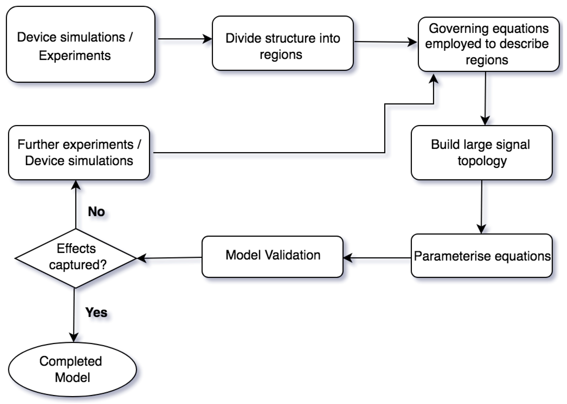
3. Models of Semiconductor Power Devices

Modeling of power semiconductor devices is essential to estimate their impact on cost, efficiency, weight, volume, and reliability, which are important performance indices of power electronic systems. These indices are mutually coupled to each other; for instance, high power densities imply high switching frequencies, which can lead to a reduction in efficiency. Prior to the fabrication of new device structures, they can be accurately investigated by modelling. It is essential to consider several physical effects with high priority for the development of power semiconductor device models, since they dominate the static and dynamic device characteristics [31,32]. In particular, the models for new devices must be able to mimic the device behavior in both static and dynamic conditions. However, if a new device shares certain related characteristics with a prevalent device, then it can be modelled by adjusting the approach of the known device [33].
A compact device modelling approach aims to predict details of the current flow across the device as a function of the applied currents and voltages, physical characteristics (geometry, doping levels), and environmental conditions (temperature and radiation) [34]. These models are based on an equivalent electrical circuit consisting of lumped circuit elements (resistors, inductors, capacitors and controlled current or voltage sources). The approach includes relations of current–voltage (I–V) and charge/capacitance–voltage (Q/C-V) for nonlinear lumped elements defined by closed-form expressions with parameter values that are based on underlying physics or extracted from experimental measurements [35]. It is paramount to achieve a good estimate to the existing association of the electrical variables. Moreover, to achieve fast simulation time, a compromise between computational speed and model accuracy is usually involved that can affect the prediction of dynamic performance of the device. Thus, the simulation time and accuracy become pivotal factors to be examined by device model engineers when considering this accord [34].
In the literature, modeling of power semiconductor devices has been reported to be performed using behavioral, semi-physics, physics-based, semi-numerical, and numerical/analytical models [34]. Behavioral models are used to represent the device behavior rather than the device physics based on functions, and are considered a good trade-off between accuracy and simulation time [36]. Using mathematical techniques and correspondent circuits, a relatively high simulation speed can be achieved by behavioral models, but physics-based understanding into the device behavior is lost [37,38]. Semi-physics models are somewhat based on device physics, wherein standard low voltage device models available from circuit simulation tools (SABER, SPICE) are remodeled to focus on the high-voltage power device design. As a consequence, the physical meaning of a few device model parameters can be lost. On the other hand, physics-based modeling tools are more accurate, but time-consuming and require many fabrication parameters.
The outline of the physics-based model approach is shown in Figure 1. In the first phase, device characterization is performed by experiments and numerical simulations on the model device structure. By analyzing the results, model equations are formulated using physics assumptions of depleted regions, field effects, charge transport, etc. The equations are parameterized using measured data as a basis and a large signal topology is built. The model is then validated by implementing for the target simulator and comparing the measured data with the simulated one. The model is considered completed only if it is able to capture the necessary effects; if not, the model should be improved and the process is repeated again [34].
Semi-numerical models can be seen as in-between physics and numerical models. In this approach, external electrical characteristics, internal physical and electrical information, carrier distribution and junction temperature in various regions of the device can be realized by applying numerical algorithms such as Laplace transformation, Fourier series, difference methods, and internal approximation to solve the ambipolar diffusion equation (ADE). Due to high level injection, the ADE is assumed to be one-dimensional, which is valid for the power semiconductor devices [39]. The numerical models provide very accurate results and can significantly contribute to the development of power devices, but are computationally intensive, complicated, and require exhaustive information on device geometry and material properties. Popular numerical simulation tools available for power devices and circuit simulation are TCAD [40,41], MEDICI [42], SILVACO [43], Sentaurus [44], etc.
Analytical models, on the other hand, are relatively quick for data processing, but have issues with improvement in accuracy. This approach is dedicated primarily for a quick evaluation of switching losses, and is based on datasheet information [38] such as input capacitances, transconductance, switching delay times and rise/fall switching times [45], or empirical formulas derived from measurements [46,47]. Langmaack et al. [48] presented a low calculation time effort approach that incorporated the use of analytical description of loss terms with numerical circuit simulations. This method has been successfully adopted for comparison of different modulation schemes and device technologies of semiconductor devices such as Si IGBT, SiC MOSFET and GaN HEMT. However, developing analytical models for switching power losses that are valid for a wide range of operating points based on datasheets or measurements is not feasible, since these losses highly depend on the parasitics associated with the circuit and package layouts.

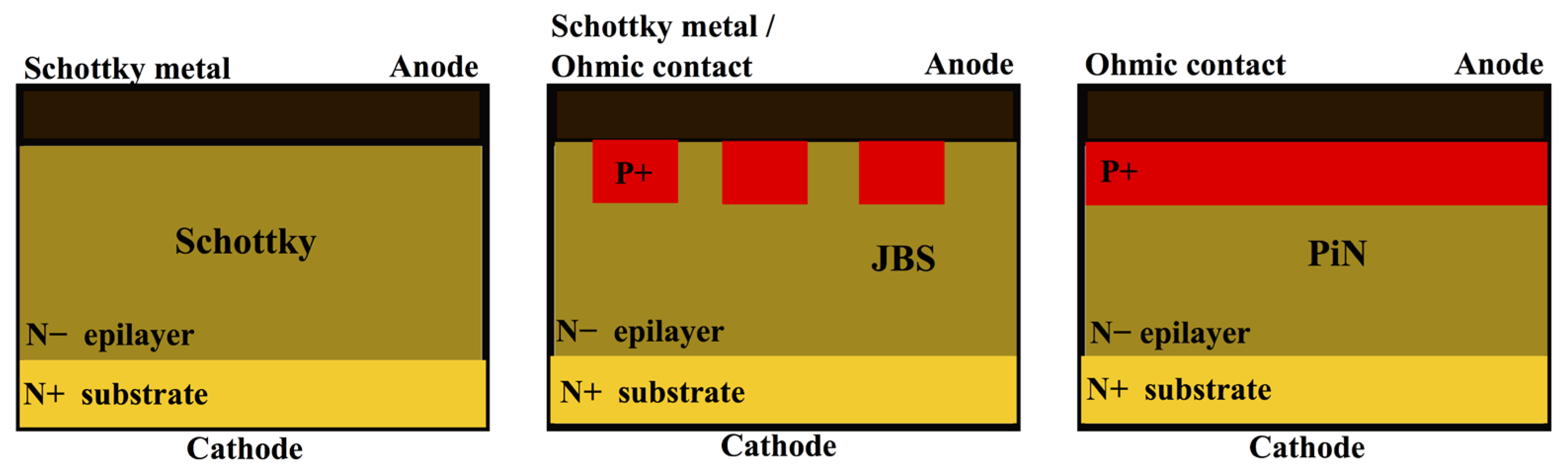
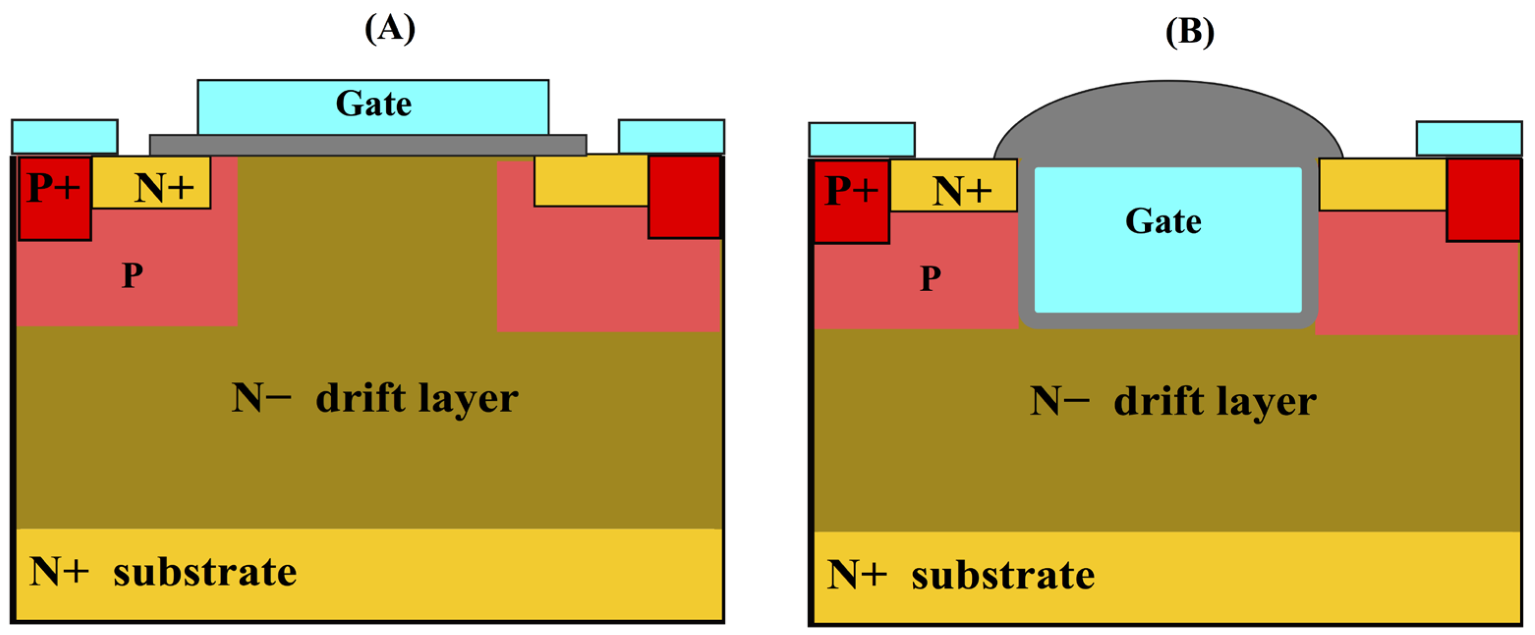
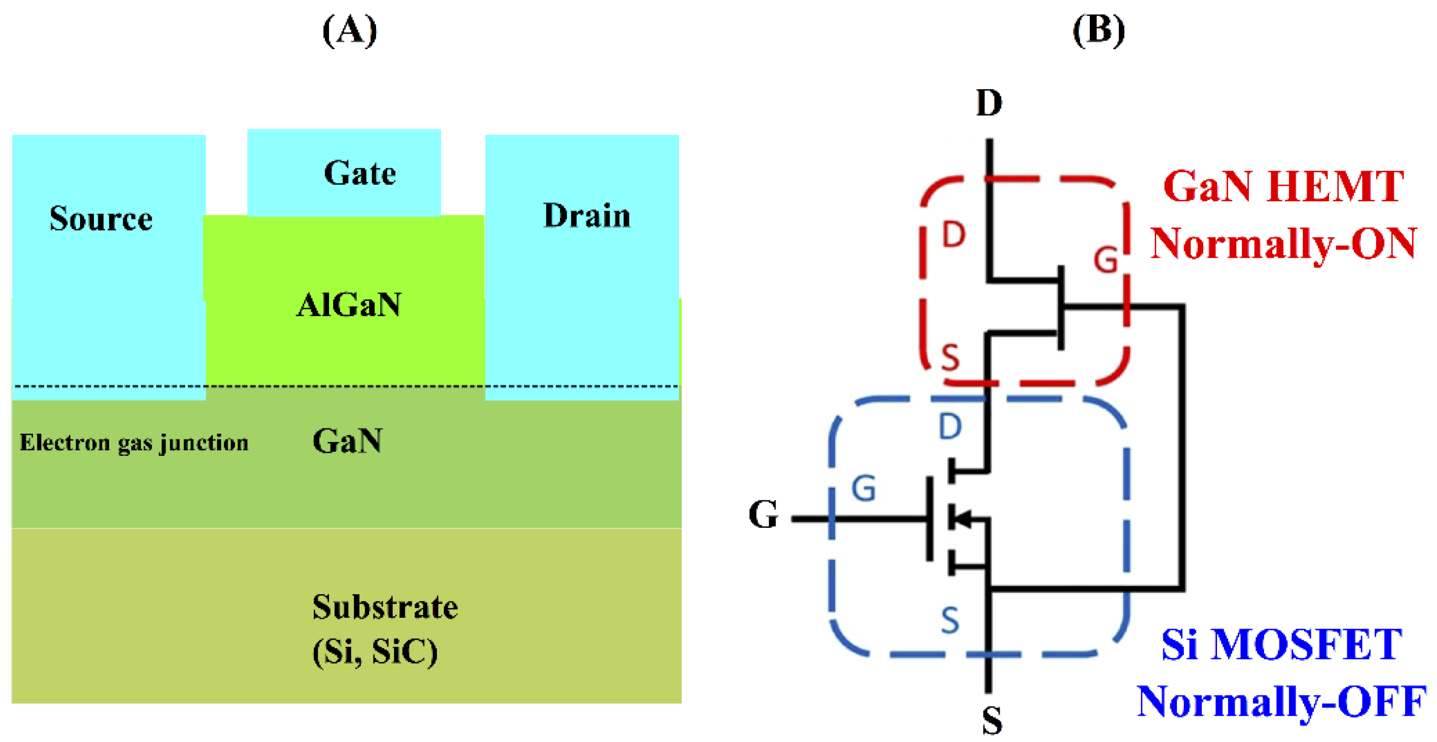
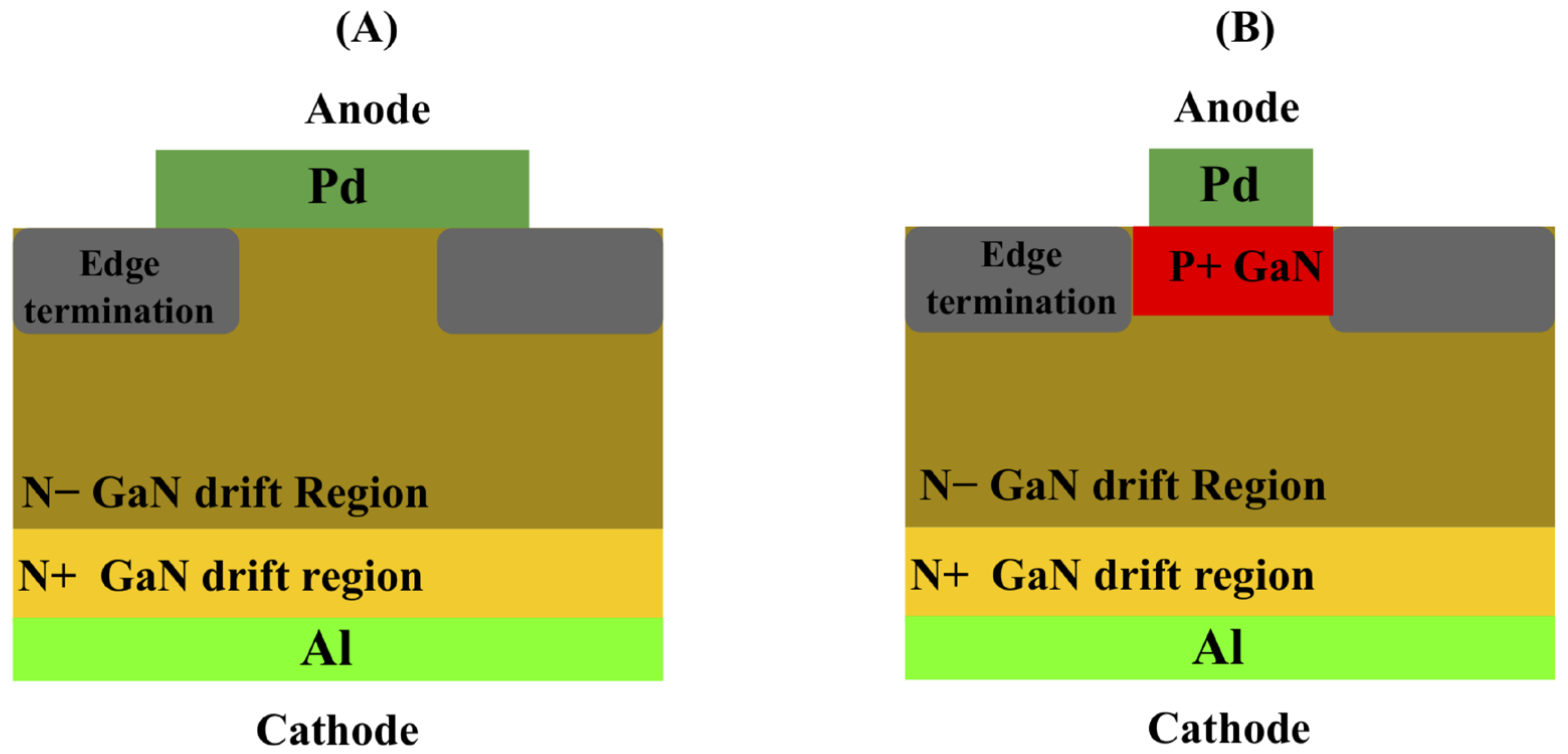
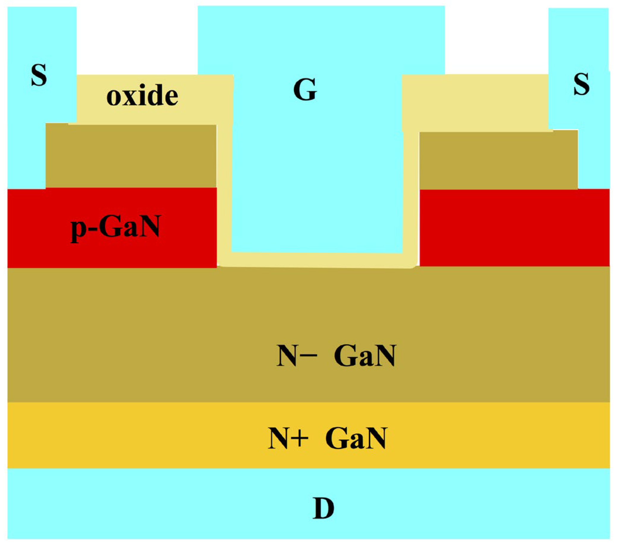
4. SiC and GaN Power Devices

Amongst WBG semiconductor materials, SiC and GaN are more appealing for high-power applications. Some SiC devices like Schottky diodes are now battling with their Si partners. The superior advantage of SiC in contrast with Si diodes permits devices to work at higher current density ratings and minimizes the size of cooling systems. By virtue of wide band gap property, devices assembled with GaN or SiC can sustain to a greater extent heat and radiation and still preserve their electrical properties. SiC has a much wider bandgap than Si and can handle higher voltages, faster switching, and display better efficiency [49]. On the other hand, GaN is especially attractive for high pressure, high temperature, and high voltage applications because of its higher electric field breakdown capability, good thermal conductivity, and high electron mobility [50,51] (Table 1).
The authors in [52] compared the performances between GaN and SiC family of power switching devices, and noted GaN to be modestly superior in providing higher power density for devices [53]. Compared to Si, the high critical field of both SiC and GaN devices is a vital feature that permits them to have reduced currents leakage and function at higher voltages [54].
SiC devices are the most prized and efficient for the next generation. Electron mobility is a feature that describes how quickly electrons can move through the semiconductor material. A significant difference can be noticed between GaN and SiC in their electron mobility (Table 1), which suggests GaN to be more suitable for high-frequency applications [55]. On the flip side, SiC has higher thermal conductivity than GaN, thus theoretically suggesting the SiC devices to operate at higher power densities than GaN. The intrinsic high temperature capabilities of SiC power devices enable better thermal management and a reduction of the volume of heat sinks and cooling systems. The capability of faster switching with lower switching losses directly implies a volume reduction of passive components and heatsinks and hence, higher power density. When high power is a key desirable device feature, SiC semiconductors have an advantage over GaN [50]. Moreover, SiC devices use fewer components and provide extensive WBG with large electric field strength, which makes it possible to achieve higher voltages with extremely low resistance per unit area and reduce the power loss extensively [56].
The focus of this paper is on WBG materials (SiC, GaN), and the material properties of diamond are briefly presented here only for comparison. Diamond has a band gap of 5.5 eV that is significantly larger than that of GaN, and hence it is termed as ultra-wide band gap (UWBG) material. Compared to WBG materials (SiC, GaN), it displays high thermal conductivity and a high breakdown field (Table 1). A comparative case study between WBG materials (SiC, GaN) and diamond for the same applications reported smaller total losses and heat sink volume, and more current density. For example, diamond devices operating at 450 K displayed 28% less losses and heatsink volume compared to 4H-SiC, and 19% lower losses and heatsink volume compared to GaN. In summary, when compared to GaN and 4H-SiC commercial devices’, the superior performance of diamond devices is primarily confined to medium-high frequency (>20 kHz), high junction temperatures (>450 K) and high-voltage (>3 kV). High cost is an obvious challenge for the commercialization of diamond as a semiconductor power device, compared to Si and other WBG material-based devices [57].

Classification of Semiconductor Power Devices

From the structure point of view, semiconductor power devices can be classified as diodes, transistors, and thyristors. For the sake of comparison between Si, SiC and GaN power devices (Table 2), we confine the discussion to diodes and transistors.
Schottky diodes are unipolar devices with low ON-state voltage drop, extremely high switching frequencies, have approximately zero reverse recovery charge and are rated at low breakdown voltage (BV < 100 V, for Si). In comparison, epitaxial Si PiN diodes are rated at BV values between 600–1200 V, and double-diffused PiN diodes at even higher BV > 1000 V [3].
SiC-based Schottky diodes are reported to be exceptionally strong in opposition to leakage current thermal runaway, since the requisite temperature leap for increasing leakage current is well overcompared to the Si PiN diode [58]. SiC power diodes can be classified primarily into three kinds: (i) SiC Schottky diode; (ii) junction barrier Schottky (JBS) diode or SiC merged PN-Schottky diode; and (iii) SiC PiN diode (Figure 2). Schottky barrier diodes (SBDs) are capable of blocking thousands of volts thanks to the larger electric field breakdown value of SiC material (Table 1). JBSdiodes are hybrid devices that integrate the engaging perquisites of high BV of PiN diodes and meager voltage of ON-state of Schottky contact. JBS diode displays Schottky-like ON-state switching characteristics and PiN-like OFF-state simultaneously. Moreover, JBS diode displays an increased surge current capability due to conduction of PiN regions at superior forward voltages. SiC JBS diodes are preferred when the blocking voltages are below 3.3 kV. SiC PiN diode is preferred over bipolar Si PiN diode because of a meager ON-state voltage dip in conditions of high current that results in conductivity modulation [34], which makes it favorable in ultrahigh voltage ranges (10–20 kV) [59].
The first SiC power switch to be marketed was SiC JFET, as its structure is simple and easy to implement. The gate terminal of SiC JFET is not isolated from the device body and there is no reliability problem of the gate oxide as observed in SiC MOSFETs. SiC JFET devices have a primarily vertical structure and, therefore, to increment the blocking voltage, the width of the drift region of the device needs to be expanded. They have normal behavior, and once the conduction channel is established, the current circulates in both directions. To achieve an adequate blocking voltage of 1.2 kV, usually the applied reverse bias gate-source voltage (VGS) ranges from −15 V to −20 V [60], allowing formation of a drain-source potential barrier by depletion of the channel region. The SiC JFET device blocks the applied high drain voltage by depleting the drift region.
The first SiC power double diffusion MOSFET was introduced in 1996 [61]. Thereafter, several SiC MOSFETs devices have been designed, characterized, and studied to improve their performance. The low resistance value between the drain and source (RDS-ON) of SiC-MOSFETs during ON mode, and no tail current during the switch off process allows it to compete with Si-IGBTs in real power applications [62].The blocking voltages reported for SiC MOSFETs are suitable for industrial operation (1200–3300 V), and the highest reported value of 15 kV [63], and display considerably reduced switching losses (over six-times) compared with the Si IGBT. SiC MOSFET structure can be classified as: (i) planar SiC MOSFET; and (ii) trench SiC MOSFET (Figure 3).
The SiC MOSFET displays a ~10-times higher electric field compared to Si MOSFET, thus a major problem is to compromise the gate-oxide reliability for low distinct RDS-ON value. For the planar structure case (Figure 3A), the peak electric field near the oxide is reduced since the gate oxide is protected by the P regions and excellent reliability performance can be achieved [64]. For the SiC MOSFET, the RDS-ON bears three primary features of resistance: (i) channel, (ii) drift region, and (iii) JFET region. The resistance of the substrate is considerable and cannot be ignored for lower voltage devices (<1.2 kV), which can be, however, minimized by using a wafer-thinning technique. For the trench structure, the low channel mobility can be upgraded, since by eliminating the JFET region, it betters the channel density of the SiC MOSFET (Figure 3B), and also the specific ON resistance is decreased.
A larger part of GaN-based power device advancement work was directed towards lateral devices, namely HEMTs (high-electron mobility transistors) (Figure 4A). This is mainly due to technological assistance of GaN HEMTs, which favor simultaneous high current, voltage, high voltage, and low ON-state resistance, thus yielding in high efficiency and high power operation. Moreover, the WBG presents a reliable and robust technology that is capable of operating at high frequency and high temperature [65]. The 2DEG (two-dimensional electron-gas junction) present in the GaN-HEMT forms an inherent channel between the drain and source of the device (Figure 4A).
In general, devices with lateral heterostructures are natively normally ON; that is, even when no gate voltage is applied, the device conducts current. This can bring up safety issues, particularly when malfunctioning of the gate driver occurs, and since the transistor is not naturally switched-off, the device could be damaged due to the uncontrolled flow of current. Moreover, circuit designs of normally ON transistors are relatively more complex due to the requirement of a negative voltage supply. Therefore, a cascode structure has been proposed to realize a normally OFF GaN HEMT, where to control a depletion-mode GaN HEMT a low-power Si MOSFET is employed. The OFF and ON state of GaN HEMT is controlled by the Si MOSFET (Figure 4B). The authors reported the cascode structure to reduce switching power loss under zero voltage switching, and addition of a low-power MOSFET would inevitably sacrifice switching speed [66]. In the lateral GaN devices, the maximum blocking voltage achievable is generally considered to be less than 1200 V, and issues related with their lateral current flow near the overlying dielectric layers and buffer layers have been reported. Moreover, due to limitations for high power applications from their lateral structures, it becomes quite challenging to achieve simultaneously very high voltages and currents for GaN HEMTs. Therefore, due to the shortcomings in performance and reliability of lateral GaN devices and to achieve the true potential of GaN, vertical devices using structures similar to their Si and SiC counterparts have been developed [67].
Novel approaches in both device engineering and materials processing have been developed for vertical GaN power devices [68]. Figure 5 shows schematic drawings of vertical GaN SBDs and PN diodes built for 600 V and 1200 V minimum BV, respectively. SBDs are built by the patterning and deposition of palladium on the epitaxial layer of GaN, and the PN diodes via in-place development of a magnesium-doped epitaxial layer of P+ GaN on top epitaxial drift region of the N-type GaN, followed by patterning and deposition of palladium to connect the P-type GaN. SBD displays a forward knee voltage of about 0.9 V, and the PN diode displays knee voltage of about 3.0 V. The two power diodes have an active area ~0.005 cm2, and are capable of managing pulsed currents in excess of 10 A [67].
Vertical GaN MOSFETs present a favorable operation by providing a normally off solution, thus surmounting an important drawback of any GaN HEMT-based construction. The structure of a vertical GaN MOSFET is shown in Figure 6.
The junction P–Nis formed amidst drain and source by p-base and n-drift regions. The reverse characteristics of the main P–N junction determines the device breakdown voltage. To better the breakdown voltage by removing the open base effect of N–P–N, the junction amidst the p-base and the n+ source region is connected to the source contact. Due to the inversion layer of the MOS structure, the channel is formed (located at the etched sidewall) [69].

5. Merits and Challenges of Using WBG Semiconductor Devices

Along with the silicon-based semiconductor, WBG semiconductors have the capability for compact, robust, and efficient power conversion systems [70]. WBG semiconductor materials in electrical power switching devices enable a transformative influence on a wide range of energy conversion applications. WBG semiconductor-based devices are thinner and display lower on-resistances, which implies lower conduction losses and an overall superior converter efficiency. From a technological point of view, SiC is the most advanced form among the current WBG power device materials. SiC has a clear advantage on higher blocking voltage, better switching speeds, and low conduction loss compared to Si [71]. WBG semiconductors are also thermally stable and their use in power switching devices permit to reduce volume, weight, and life cycle costs [72].
WBG provides many advantages like handling higher voltages and power, faster switching, better efficiency, and higher operating temperatures [73]. Power devices with semiconductor material SiC have less effect on functionality, and continue to work even when the temperature rises up to 600 °C [74]. WBG semiconductor-based power devices are more reliable as with temperature and time only slight fluctuation is noted in its forward and reverse characteristics. WBG power devices are smaller, faster, and more reliable and operate on higher frequencies, power levels, and higher voltages [75]. WBG semiconductor devices have better efficiency and enable high-power density converters, exhibit superior power operating speeds, and an improved efficiency for power conversions [70,76,77].
For high-power applications, SiC MOSFETs display superior switching speed, and thus operate at higher switching frequencies than Si IGBTs [78]. GaN-based HEMTs function at switching frequencies higher than that of Si MOSFETs, considering low-power applications [79,80,81]. The extremely fast switching and the material properties of WBG devices have posed new challenges to their applications. The major challenges include switching frequencies in the hundreds of kHz to MHz range, rapid current and voltage slopes triggering the effects of capacitive couplings and parasitic inductive, and unusual electromagnetic interference (EMI) emission. By virtue of high switching frequency, WBG power devices are more susceptible to EMI, a phenomenon that occurs when an electronic device is exposed to an electromagnetic (EM) field [82,83]. Despite the fact that for applications requiring high-power, the switching frequencies are not as high compared to applications requiring low-power, EMI still remains notable since the amplitude of switching voltages and currents are high. On the contrary, for low-power applications, the magnitude of switching currents and voltages can be smaller than those in high-power, however, since the devices operate at a high frequency EMI’s presence is significant [84]. EMI propagation paths and EMI noise source characteristics are key to compare the EMI performance of Si devices and WBG devices. Tretin et al. [85] compared conductive EMI between matrix converters with Si IGBTs (switching speed 6.6 kV/μs) and SiC MOSFETs (11 kV/μs) at 10 KHz switching frequency. The EMI noise of SiC MOSFET was found to be 20 dB higher compared to Si IGBT from 10–30 MHz [85]. For a 1kW 400 V GaN HEMT device, the conducted EMI measured was found to be 20 dB higher at 500 KHz switching frequency compared to EMI at 50 kHz switching frequency. Thus, the conductive EMI is the most severe when WBG devices function at higher switching frequency and speed compared to Si-devices [86].
To reduce the noise-levels generated by the power converters, most devices contain an EMI passive filter whose use remains a challenge towards enabling high power density [87]. EMI shielding is a process that involves preventing the penetration of the harmful EM radiations into the electronic devices [88]. It is one of the best methods to protect the health of living beings as well as the environment from the negative impacts of EM waves [89]. The passive filter occupies nearly 30% of the power electronics converter system’s volume and its use is inevitable to guarantee compliance with conducted EMI standards. To reduce the submissive EMI filter volume is a big task for the power generator designers [90]. Active EMI filters (AEF) in this context display great promise in minimizing the volume of the passive component (with reductions higher than 50%) in power converters [91,92,93]. In [94], the authors provided an overview of several works in the area of AEFs and their implementations for different power converters in the past three decades. The topology of AEFs [95] are built on rating of sensing and cancellation components and kind of source and load impedances. Other techniques such as using small propagation paths and by using small passive components have also been suggested to reduce the system’s volume [96]. However, the most common EMI problems are power disturbances because of different filters [97], due to which units, circuits, and wires can never contain complete electricity, and EMI shielding currently has a bigger concern. Moreover, an EMI filter’s performance at high frequency is restricted by the filter’s parasitic parameters and the magnetic material, thus making it challenging to reduce high frequency EMI noise [98].

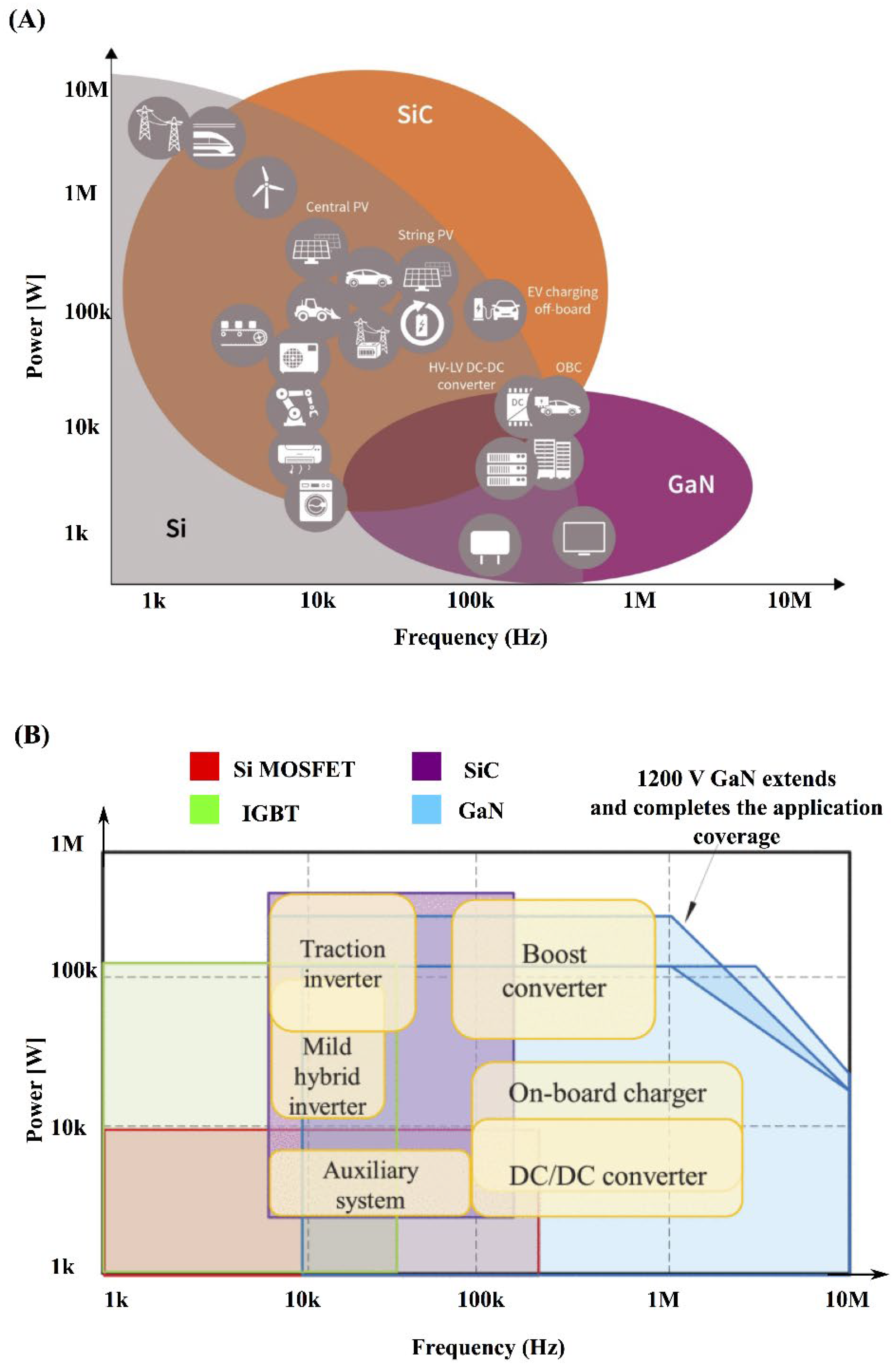
6. Applications of WBG Devices

In this section, four applications of WBG devices are reviewed. In the first application, the Si and the WBG devices are employed at the same time, in a device or in a circuit level, to gain the superior figure of merit (FOM) of the WBG devices, and solve their drawbacks such as higher cost, limited current rating, etc., thanks to the presence of the Si devices. Such a combination of devices with different semiconductor technologies is titled as the hybrid application. Electric vehicles are the second application, where WBG devices can play an important role to promote this developing industry, in accordance with the growing demand and the global politic of replacing conventional combustion engine vehicles with electric ones. As the efficiency and the power density of the power electronics interfaces in the electric vehicles are crucial, WBG devices have a great chance to increase their share in this market. Same as the application of the electric vehicles, the employment of the WBG devices is increasing in the motor drive application. That is also because of this fact, that the voltage/current ratings of the available commercial WBG devices are in the same range of those of motor drive applications. Therefore, the application of a WBG device in the motor drive is studied as the third application in this section. The fourth application is devoted to the renewable energy systems, where because of higher range of voltage/current, the employment of the WBG devices is more challenging, especially in the case of GaN. This is reviewed in the last part of this section.

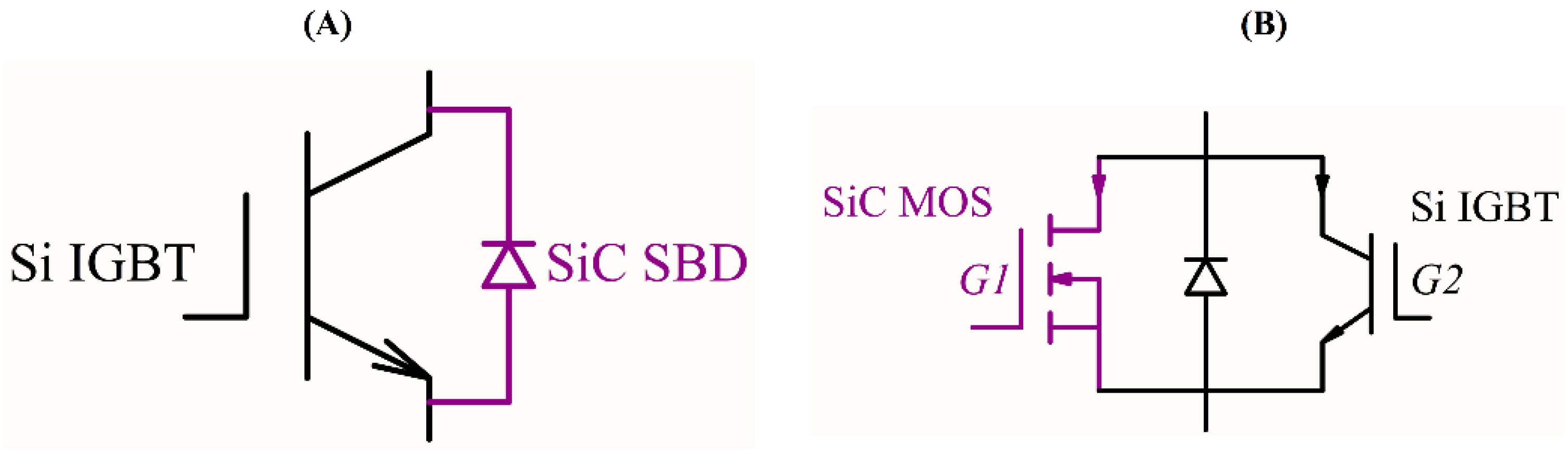
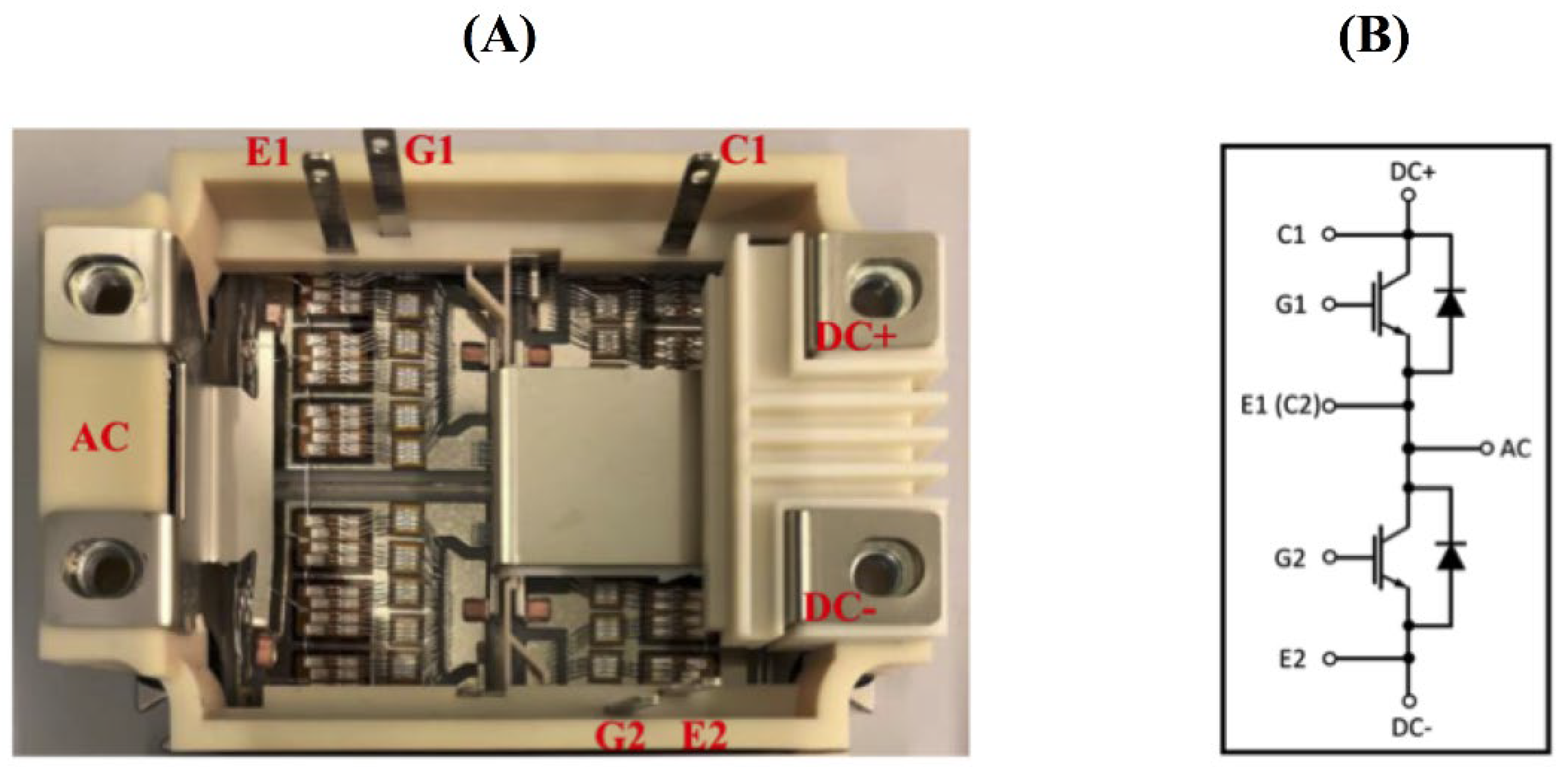
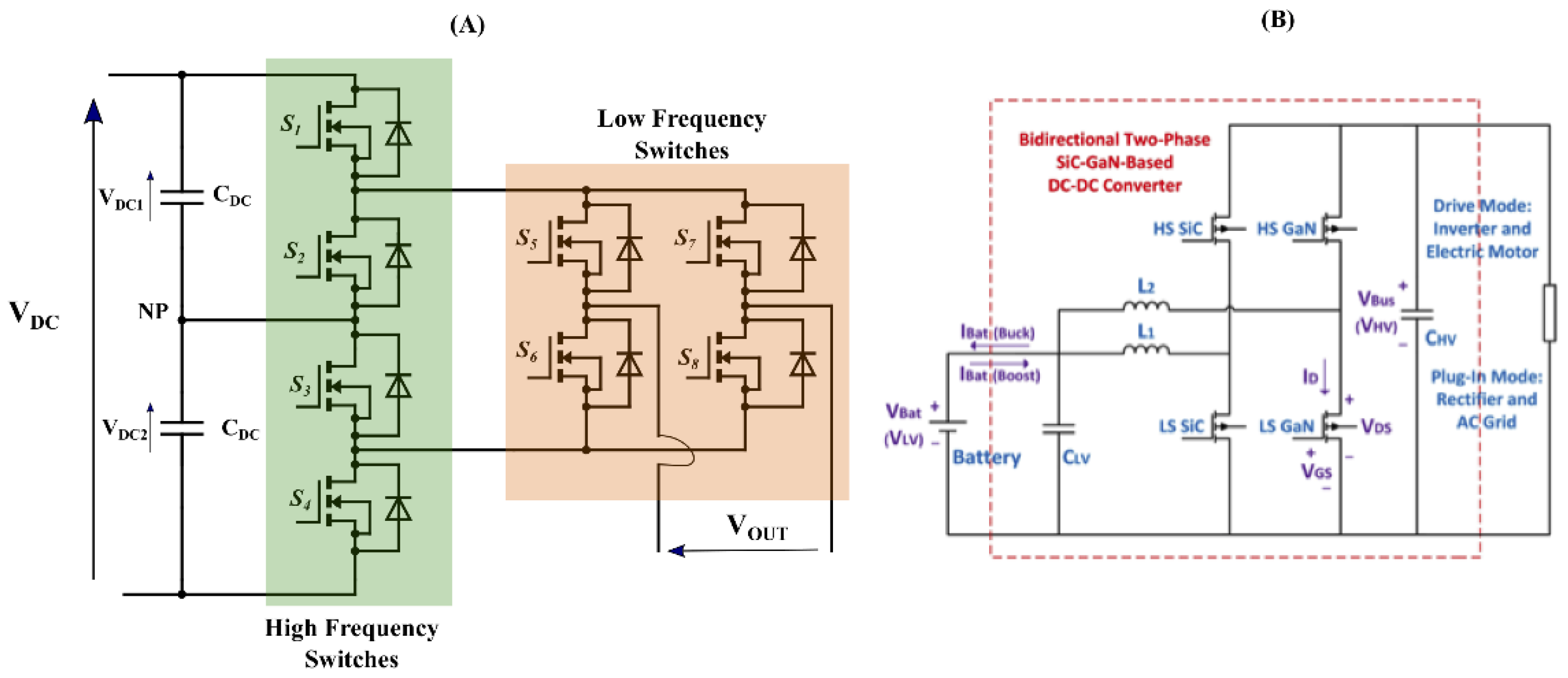
6.1. Hybrid Application of WBG and Si Devices

Figure of merit (FOM) superiority of WBG devices over Si devices results in higher efficiency and higher power density in different applications. Still one of the main drawbacks of current WBG devices in the market is their higher cost with respect to that of Si devices. It arouses the idea of hybrid utilization of WBG and Si devices in device, module, and circuit levels [99].
In device level, there are three examples as follows:
(i)
The use of a SiC Schottky Barrier Diode (SBD) as the anti-parallel diode of a Si IGBT (Figure 7A). It is because of better reverse recovery performance of SBD with respect to that of Si diodes [100].
(ii)
Device paralleling of a Si IGBT and a SiC MOSFET (Figure 7B). In this way, Si IGBT’s low conduction loss characteristics and SiC MOSFET’s low switching loss characteristics are combined in high current application with a compromised cost [101].
(iii)
Similar to the previous example, GaN HEMT can be paralleled to both Si IGBT [102] and Si MOSFET [103]. The achievements (better conduction/switching performance with a reasonable cost) are the same as the previous example as well.
In the module level, WBG and Si devices are manufactured in a module. This results in the module being less sensitive to the junction temperature. Since the SiC SBD removes the temperature-dependency during the turn-ON, there is a significant loss reduction at high temperature [104]. Moreover, hybrid modules have less parasitic packaging inductances, higher power level, and lower power losses compared to Si-based modules. The most common configuration for hybrid modules is the integration of Si IGBT and SiC SBD, as it can be seen in Figure 8 [105].
A commercial example of such a hybrid module is F3L400R10W3S7F by Infineon, where Si IGBTs are integrated with SiC diodes, for high power (950 V 400 A) active three-level neutral point clamping (ANPC) inverter applications. When using SiC MOSFETs instead of Si IGBTs, an important improvement arises from the different forward characteristics. The unipolar structure of the MOSFET gives a linear (ohmic) characteristic, which is beneficial especially for low and partial load conditions [106,107,108].
In the circuit level, there are examples in different applications such as multilevel inverter for motor drive and dc-dc converter for power management in electric vehicles (EVs). In [109], a single-phase five-level ANPC inverter is proposed where Si and SiC MOSFET (Figure 9A) are employed in order to improve both efficiency and power density.
In [110], a hybrid configuration, using SiC MOSFET and GaN FET, is proposed as the power management dc-dc converter of EVs. GaN FET has one of the lowest switching losses among all devices. Therefore, it is the best candidate for hard-switching applications. However, due to the lateral structure of the commercially available GaN devices, their power level is limited to 15 kW. As a large sedan will need a power level of 150 kW, SiC MOSFET and GaN FET can be employed as it is shown in Figure 9B. In this way, for low load, only GaN will conduct, while in high load, both SiC and GaN will share the current unequally.

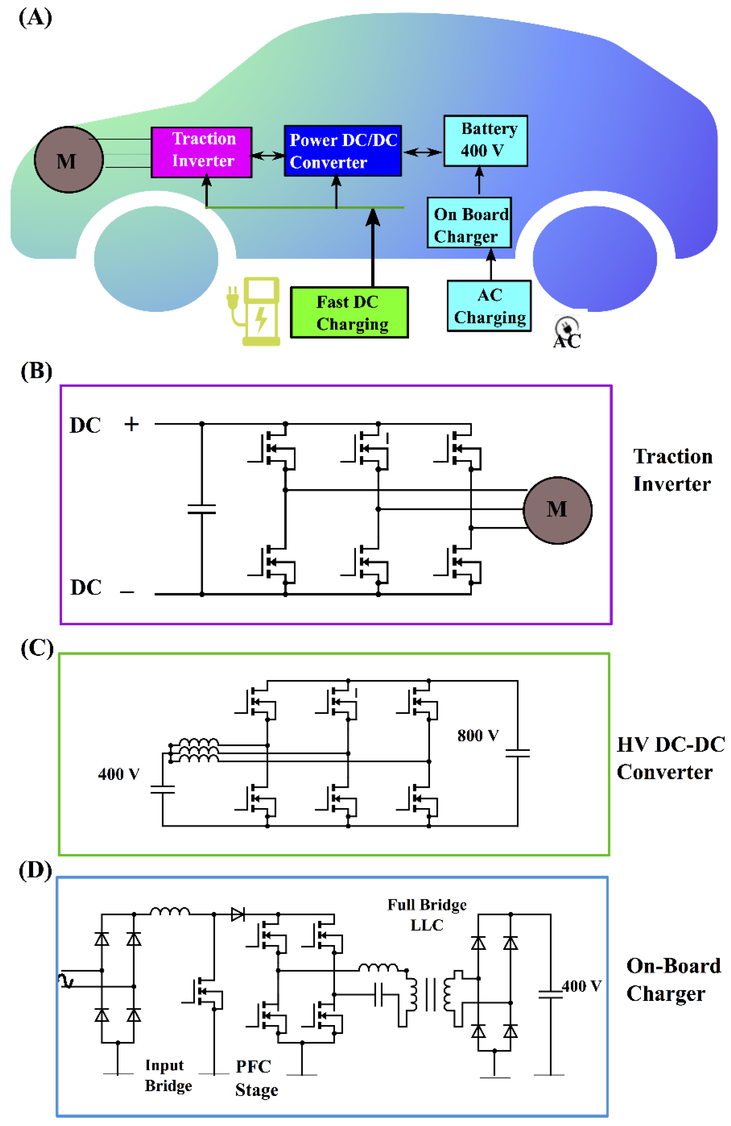
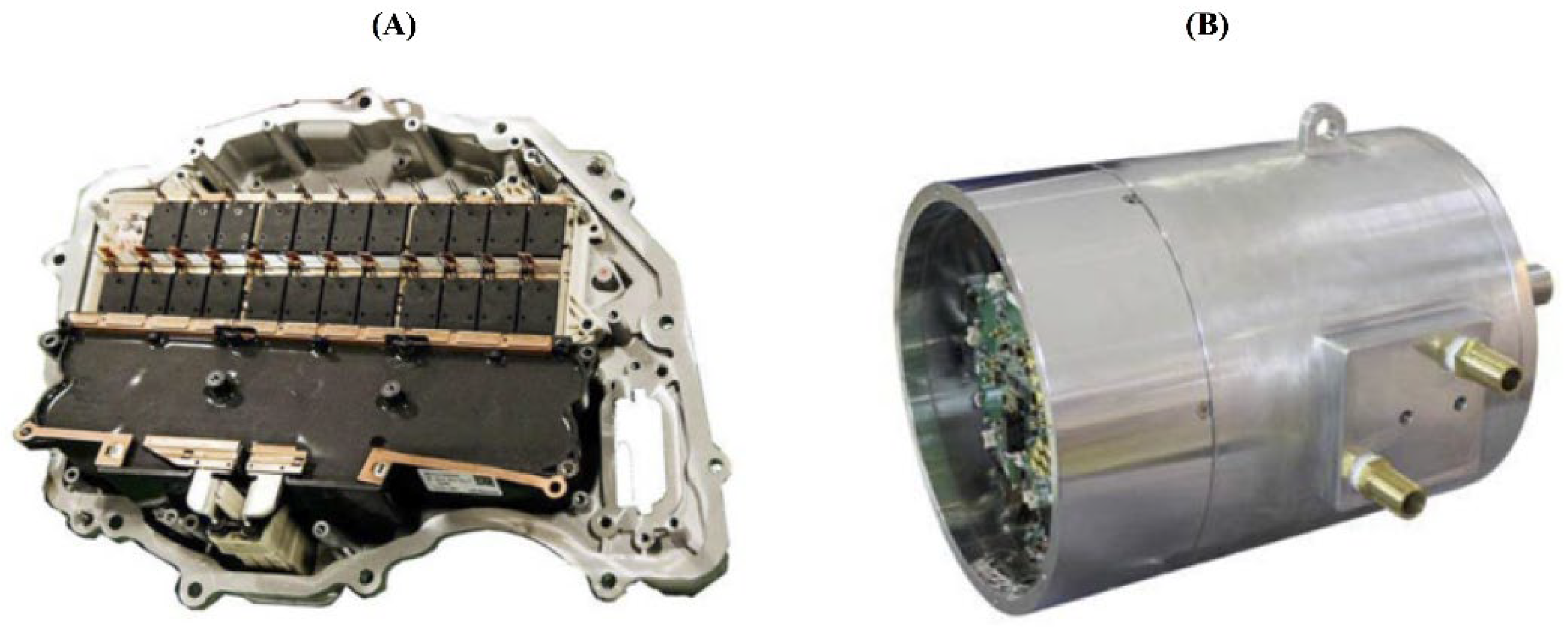
6.2. WBG Devices in Electric Vehicles (EVs)

It is a good idea to study the application of WBG devices in EVs, based on power ratings of different power electronic interfaces in an EV. In Figure 10, it can be seen that SiC competes with Si in a higher range of power, but lower range of frequency, while GaN competes with Si in a lower range of power, but high range of frequency applications [111].
Therefore, if we study the power electronic interfaces in an EV, then we can realize the right place for SiC and GaN there. In Figure 11, an overview of the EV ecosystem with the three main subsystems is shown. The traction drive inverter (Figure 11B) and the power management DC-DC converter (Figure 11C), the interface between the battery package and the inverter, are considered as high-power applications with the power range of 60 to 150 kW depending on the model [112]. For the on-board battery charger (OBC) (Figure 11D), including the dc-dc converter and ac-dc rectifier, the trend of fast charging leads to the designs up to 22 kW [113]. In the case of AC charging, the power level is up to 43.5 kW [114]. The power range of the air conditioner is in the range of 5 kW as well. Both the battery charger and the air conditioner are considered as medium power applications in an EV. In addition, there are auxiliary loads in an EV with a low range of voltage (12 to 40 V) and low range of power (up to 3 kW). It can be concluded that SiC devices are suitable for the traction inverter, the power management DC-DC converter, and the fast-charging OBCs (high power/voltage) and GaN devices are suitable for the low-to-medium charging speed OBCs, the air conditioner, and the auxiliary loads (low-to-medium power/voltage) (Figure 10B).
Thus far, there are some commercial examples of the WBG-based EVs such as: (i) Full-SiC power module in Model 3 by Tesla (Figure 12A) [115]; (ii) SiC-based traction inverter and power management dc-dc converter in Camry by Toyota as a road test prototype in 2015; (iii) an All-GaN inverter buggy vehicle by Nagoya University and Toyota as a road test prototype [116]; and (iv) an integrated SiC EV drive system by Mitsubishi Electric (14.1 L 60 kW) [117], shown in Figure 12B, with thermal resistance improvement between the motor drive system and the cooling system.
In Table 3, a comparison between WBG- and Si-based devices for different EV subsystems is shown [116]. It is evident from the parameters presented in Table 3 that WBG-based devices display superior characteristics compared to Si-based devices in the EV subsystem.

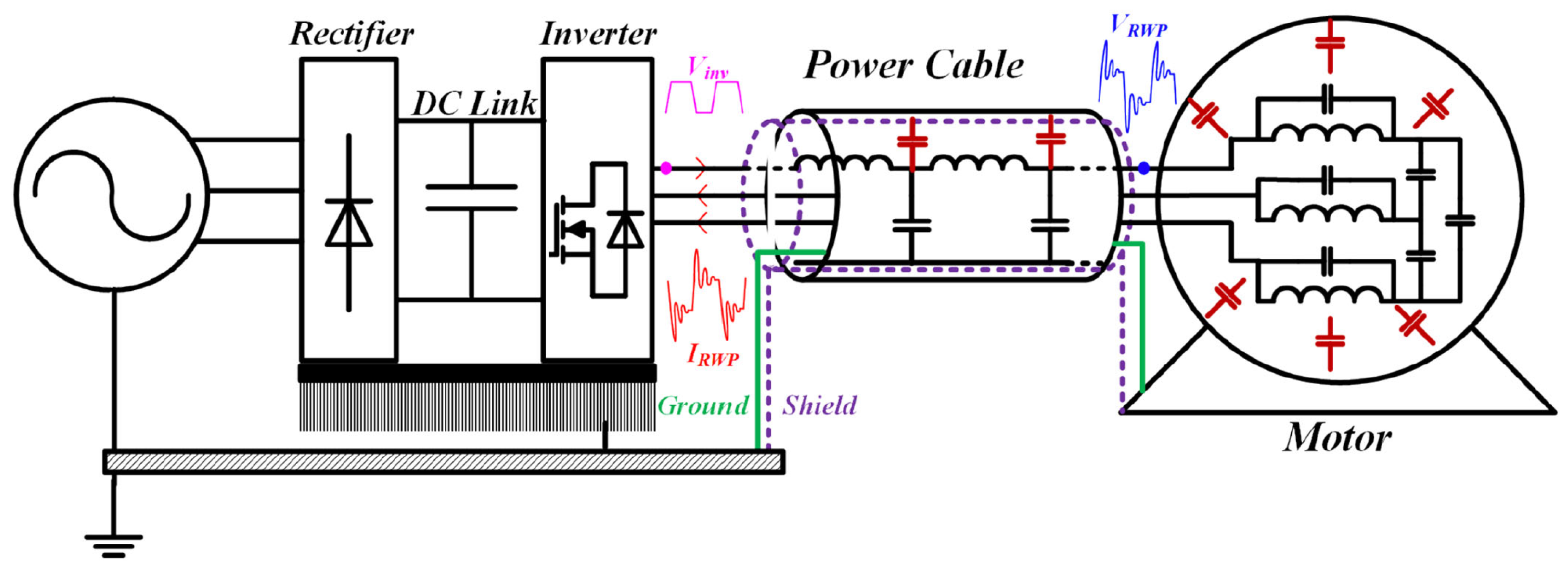
6.3. WBG Devices in Motor Drive Applications

WBG devices provide various improvements in motor drive applications. The primary three advantages are: (i) high switching frequency ability of WBG devices, resulting in low current ripple, which is a requirement for low-inductance machines, (ii) high switching frequency ability of WBG devices, resulting in high fundamental frequency of output current, which is a requirement for high-speed machines, and (iii) high junction temperature capability of WBG devices, resulting in high junction temperature operation, and a reduced-size cooling system, which is a requirement for motor drive systems operating in high ambient temperatures. In Table 4, the three categories, low inductance, high speed, and operation at high ambient temperature, are listed [118].
However, the general advantages of WBG devices are valid also for motor drive systems, which are: (1) higher efficiency, because of lower conduction and switching losses of WBG devices, and (2) higher power density, because of the smaller size of passive components, due to the higher switching frequency capability of WBG devices. One of the main challenges in motor drives is motor terminal overvoltage, caused by reflected wave phenomena (RWP), especially when the motor is fed from the inverter, connected by long cables. The overvoltage appears at motor terminal and damages the motor insulation. The amount of the overvoltage depends on switching time of the invert devices and the cable impedance. The RWP is depicted in Figure 13, where in a typical cable-fed AC drive, the motor terminal voltage VRWP has overvoltage compared to the inverter voltage Vinv. In the case of WBG devices, as the switching time is much faster with respect to that of Si devices, the high dv/dt is more crucial. Therefore, particular care should be considered [119].
As filtering is a bulky and costly solution, a software-based intelligent solution is preferred. For instance, a modified PWM method is proposed in [120] to combat the RWP, caused by high switching speed of SiC-based inverters. In a conventional single-phase PWM inverter, the inverter voltage is modulated only between two level: +VDC and −VDC. In [120], the inverter voltage is also modulated at a third level (Vinv = 0) for a time period called dwell time (td) equal to two times of the propagation time (tp). The propagation time is the time when Vinv travels through the cable and arrives at the motor terminal (VRWP). In this way, the reflected voltage can be counterbalanced, instead of being doubled, at the motor terminal. There are some industrial examples of the application of WBG devices in motor drives. The KSB group introduced an integrated motor drive (IMD) in 2017, which is a 22 kW ultra-compact high-efficiency system, consisting of a synchronous reluctance motor and a SiC-based inverter. In integrated motor drives, the power electronic interface is in the same housing with the motor. As a result, the compactness is the key factor for the design. It is more challenging when it comes to WBG-based drives. An example of a compact high-efficiency SiC-based IMD is a distributed servo drive system by Beckhoff in 2017 [121].
Recently, Langmaack et al. examined the use of wide band gap devices for an electrical turbo compressor unit for fuel cell applications [122]. A detailed analysis in terms of efficiency, frequency, and power density for different circuit topologies and device technologies was performed to identify a high performance drive inverter for a fuel cell turbo compressor [123]. Their analysis suggested that adopting SiC MOSFET power modules with simple topology in inverter design resulted in high power density and good efficiency compared to the silicon-based solution with a complex circuit topology [124].

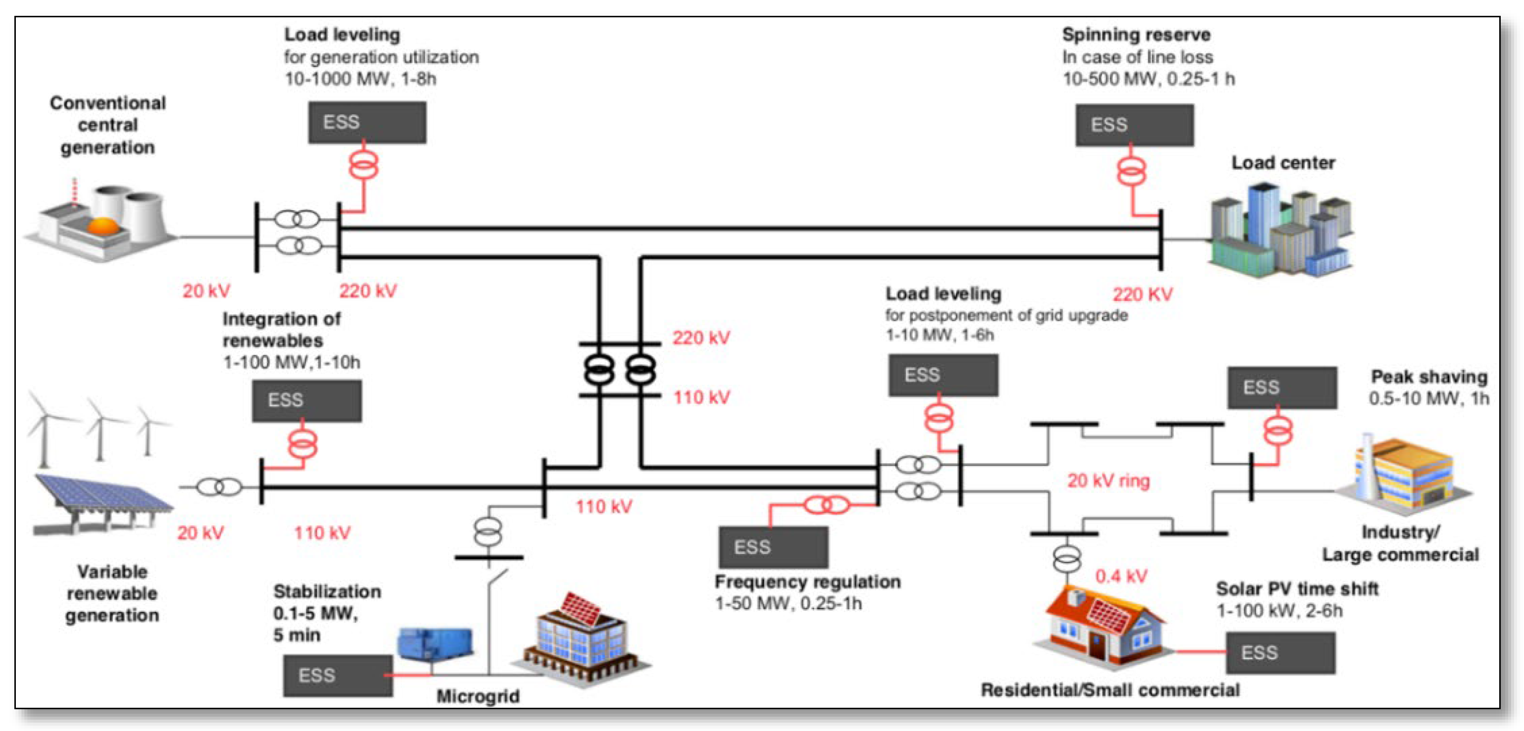
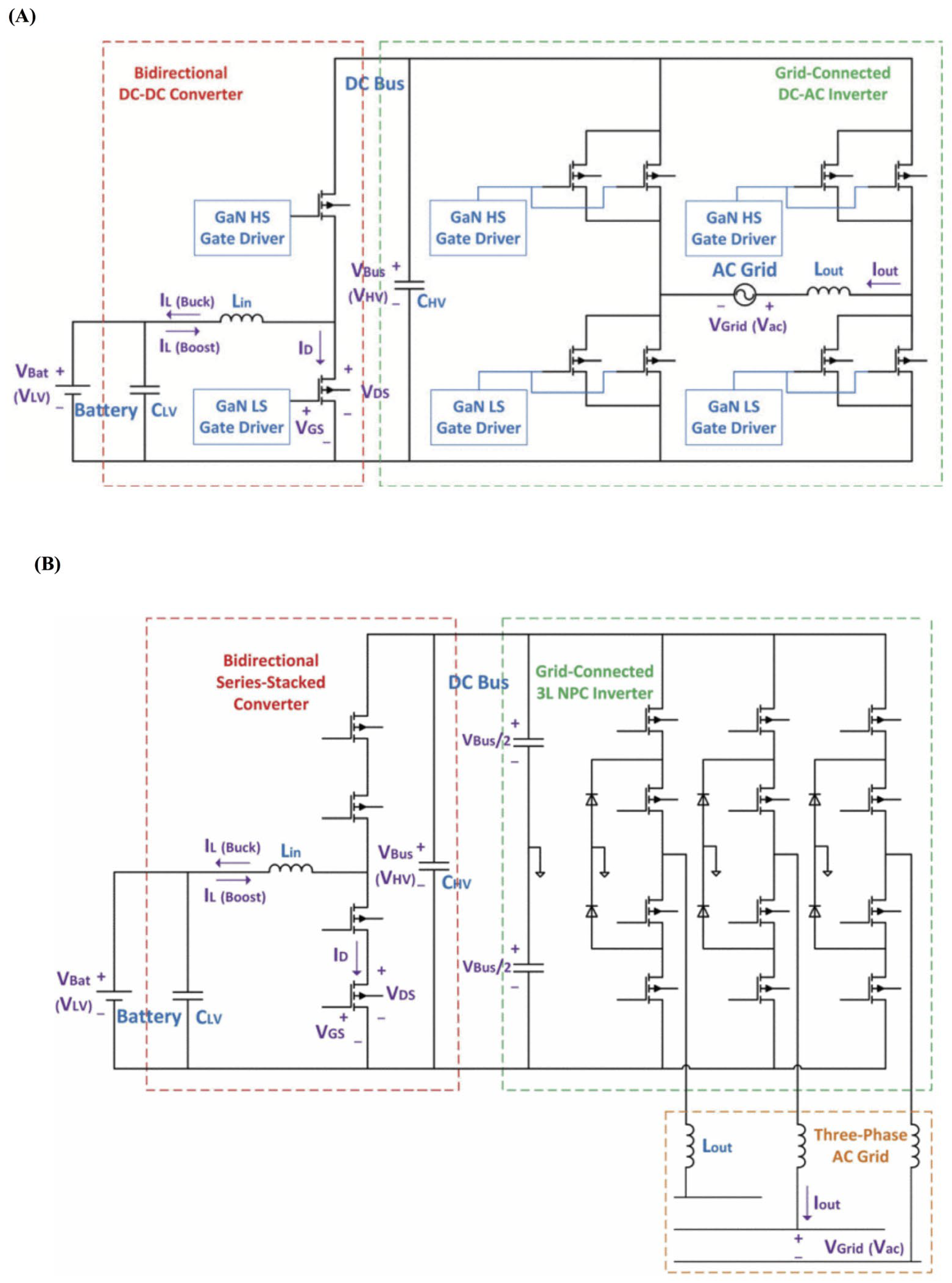
6.4. WBG Devices in Renewable Energy Systems

In photovoltaic (PV) systems [125,126,127], wind turbine systems [128], and battery energy storage systems (BESS), WBG devices can play an advantageous role to increase efficiency and power density. The main challenges, however, are electromagnetic compatibility (EMC) issues, high transient voltage/current (dv/dt and di/dt), and system cost [128]. Another important matter in this context, is the power rating of renewable energy systems (RESs) and corresponding voltage/current rating of WBG devices. PV systems can be classified by their power rating, as is shown in Table 5.
The configuration of BEES (or simply energy storage systems, ESS) is also shown in Figure 14, based on their power rating, by ABB [129]. By studying Figure 14, the potential employment of WBG devices can be investigated, based on their power/voltage ratings. The configuration of BEES (or simply energy storage systems, ESS) is shown in Figure 14, based on their power rating, by ABB [112].
Considering the power rating of RESs and voltage/current rating of WBG devices, the advantage of WBG devices can be obtained more easily in the low-to-medium power range (1 to 100 kW), such as that of the residential/small commercial RES application, that is shown in Figure 14.
In [130], a 50 kW SiC-based inverter is proposed for rooftop PV systems, where a desirable power density of 1 kW/kg is achieved. In [131], 650 V GaN devices are discussed for 400 VDC microgrid BESS. However, there are efforts in order to employ WBG devices for high power applications as well. For example, in [132], an all-SiC boost converter is used in a 1 MW solar inverter, where the inverter itself has a three-level T-type neutral-point-clamped structure, which is Si-based. In [133] also, a SiC device is applied in a BEES with a multi-level converter for a MW power 13.8 kV voltage distribution system. There are also industrial examples of the application of WBG devices for RES. General Electric has installed the first prototype all-SiC 1 MW solar inverter in Berlin [134], already switching solar electricity from DC to AC, and shows the best-in-class efficiency using an air cooled design with simpler topology and controls (Figure 15).
Due to higher switching frequency, the filter size is reduced and the overall megawatt-scale solar inverter system optimization resulted in a lower cost solution [135]. There are solutions in order to deal with the challenges and the limitations of using WBG in RES. In [136], the hybrid use of SiC MOSFET and Si IGBTs is proposed, where a SiC MOSFET is in parallel with three Si IGBTs, all of 100 A/1.2 kV current/voltage ratings, for a 250 kW solar/wind inverter, in order to take advantage of the high efficiency SiC in low to medium loads, and keep the overall cost of the system low, at the same time. GaN devices have the lowest switching losses for the hard-switched applications; however, their current/voltage ratings (100 A/650 V) are even lower than those of SiC. To achieve the high efficiency of GaN devices and cope with their low current/voltage ratings, device paralleling and device series stack structure are proposed in [137,138], for the application of single-phase and three-phase residential BEES, respectively.
Figure 16A shows device paralleling for a single-phase RES application with two power stages: a bidirectional DC-DC converter and a single-phase two-level inverter, where the latest one employs GaN device paralleling. Figure 16B shows a series-stacked structure for a three-phase RES application with two power stages: a bidirectional DC-DC converter and a neutral-point-clamped (NPC) three-phase inverter, where in the first power stage, series-stacked GaN devices are employed.

7. Conclusions

This paper provides a detailed review on the potential of wide band gap semiconductor devices in power electronics. WBG materials such as GaN and SiC have seen an upsurge and are projected to be widely adopted in the semiconductor device market. These materials find their use across many industries depending on their device power ratings. In semiconductor devices rated from 15 V to 650 V, Si remains a strong candidate, while being also reliable and economical. SiC is more suitable for high power applications (e.g., dc-dc converters in electric vehicles), and GaN for low power applications (e.g., mobile device chargers). They are being studied as an alternative to silicon primarily due to their interesting electrical properties, such as three times higher band gap and around ten-fold higher critical electric field compared to that of Si. WBG-based devices are smaller in size by virtue of ten times thinner drift layers compared to Si devices of a specific voltage capability. Moreover, the higher switching frequency of SiC and GaN devices allows reducing the size of passive components that leads to an overall decrease in the size of the system. The reduction in the size would imply requiring fewer materials that will make WBG devices more sustainable. The cost of WBG materials remains a challenge as the devices are 2–3 times more expensive than Si-based devices. Therefore, to make them cost-competitive against Si counterparts, the demand and manufacturing of WBG devices need to start to gather pace. Indeed, the WBG semiconductor devices market size, which is valued at $1.35 billion in 2022, is expected to become around $6.3 billion by 2028. In the near future, WBG devices will continue to make progress into the predominant position of the Si-based devices and unleash innovative solutions for power electronics systems that are unattainable with silicon technology.

Author Contributions

Conceptualization, A.K. and G.G.; formal analysis, A.K., M.L. and R.B.; data curation, A.K. and M.M.; writing—original draft preparation, A.K. and M.M.; writing—review and editing, A.K., M.M., M.L., S.R., W.-T.F., R.B. and G.G.; funding acquisition, W.-T.F. and G.G. All authors have read and agreed to the published version of the manuscript.

Funding

This research was partially funded by Autonomous Regionof Sardinia within the ICTprojects SMART AMP—“Smart Area Marina Protetta Capo Carbonara”. POR FESR Sardegna 2014–2020, CUP: F26C18000520006, to University of Cagliari (Scientific Manager G. Gatto). This research was funded by Interreg Deutschland-Denmark from the European Regional Development Fund via the PE-Region Platform project (ref. 098-1.1-18) to M. Moradpour and W. T. Franke. Further information on www.interreg5a.eu (last accessed on 30 November 2022).

Institutional Review Board Statement

Not applicable.

Informed Consent Statement

Not applicable.

Data Availability Statement

Not applicable.

Acknowledgments

The authors thank Andrea Vincis, Technologist at University of Cagliari for his constant technical and administrative support.

Conflicts of Interest

The authors declare no conflict of interest. The funders had no role in the design of the study; in the collection, analyses, or interpretation of data; in the writing of the manuscript, or in the decision to publish the results.

Correction Statement

This article has been republished with a minor correction to the existing affiliation information. This change does not affect the scientific content of the article.

References

  1. Desogus, G.; Quaquero, E.; Rubiu, G.; Gatto, G.; Perra, C. BIM and IoT Sensors Integration: A Framework for Consumption and Indoor Conditions Data Monitoring of Existing Buildings. Sustainability 2021, 13, 4496. [Google Scholar] [CrossRef]
  2. Roccaforte, F.; Fiorenza, P.; Greco, G.; Lo Nigro, R.; Giannazzo, F.; Iucolano, F.; Saggio, M. Emerging trends in wide band gap semiconductors (SiC and GaN) technology for power devices. Microelectron. Eng. 2018, 187–188, 66–77. [Google Scholar] [CrossRef]
  3. Gachovska, T.K.; Hudgins, J.L. SiC and GaN Power Semiconductor Devices. In Power Electronics Handbook; Butterworth-Heinemann: Woburn, MA, USA, 2018; pp. 95–155. [Google Scholar] [CrossRef]
  4. Cao, Y.; Pomeroy, J.W.; Uren, M.J.; Yang, F.; Kuball, M. Electric field mapping of wide-bandgap semiconductor devices at a submicrometre resolution. Nat. Electron. 2021, 4, 478–485. [Google Scholar] [CrossRef]
  5. Juneja, S.; Pratap, R.; Sharma, R. Semiconductor technologies for 5G implementation at millimeter wave frequencies—Design challenges and current state of work. Eng. Sci. Technol. Int. J. 2021, 24, 205–217. [Google Scholar] [CrossRef]
  6. Ren, A.; Wang, H.; Zhang, W.; Wu, J.; Wang, Z.; Penty, R.V.; White, I.H. Emerging light-emitting diodes for next-generation data communications. Nat. Electron. 2021, 4, 559–572. [Google Scholar] [CrossRef]
  7. García de Arquer, F.P.; Talapin, D.V.; Klimov, V.I.; Arakawa, Y.; Bayer, M.; Sargent, E.H. Semiconductor quantum dots: Technological progress and future challenges. Science 2021, 373, eaaz8541. [Google Scholar] [CrossRef]
  8. Gatto, G.; Marongiu, I.; Perfetto, A.; Serpi, A. Modelling and predictive control of a Buck-Boost DC-DC converter. In Proceedings of the Speedam 2010, Pisa, Italy, 14–16 June 2010; pp. 1430–1435. [Google Scholar]
  9. Stefanik, J.; Zygmanowski, M. Power Loss Analysis of Advanced-Neutral-Point-Clamped Converter with SiC MOSFETs and Si IGBTs. In Proceedings of the 2021 IEEE 19th International Power Electronics and Motion Control Conference (PEMC), Gliwice, Poland, 25–29 April 2021; pp. 161–166. [Google Scholar]
  10. Casula, G.A.; Montisci, G.; Valente, G.; Gatto, G. A Robust Printed Antenna for UHF Wearable Applications. IEEE Trans. Antennas Propag. 2018, 66, 4337–4342. [Google Scholar] [CrossRef]
  11. Mazumder, S.K.; Kulkarni, A.; Sahoo, S.; Blaabjerg, F.; Mantooth, H.A.; Balda, J.C.; Zhao, Y.; Ramos-Ruiz, J.A.; Enjeti, P.N.; Kumar, P.R.; et al. A Review of Current Research Trends in Power-Electronic Innovations in Cyber–Physical Systems. IEEE J. Emerg. Sel. Top. Power Electron. 2021, 9, 5146–5163. [Google Scholar] [CrossRef]
  12. Millan, J.; Godignon, P.; Perpina, X.; Perez-Tomas, A.; Rebollo, J. A Survey of Wide Bandgap Power Semiconductor Devices. IEEE Trans. Power Electron. 2014, 29, 2155–2163. [Google Scholar] [CrossRef]
  13. Castellazzi, A.; Gurpinar, E.; Wang, Z.; Suliman Hussein, A.; Garcia Fernandez, P. Impact of Wide-Bandgap Technology on Renewable Energy and Smart-Grid Power Conversion Applications Including Storage. Energies 2019, 12, 4462. [Google Scholar] [CrossRef]
  14. Lin, Q.-L.; Liang, H.; Zhou, C.-Q.; Qian, Z.-F.; Sun, Y.-L.; Wang, X.-Y.; Wang, R.-H. Defect-induced magnetism in χ3 borophene. Rare Met. 2022, 41, 3486–3494. [Google Scholar] [CrossRef]
  15. Roccaforte, F.; Giannazzo, F.; Iucolano, F.; Eriksson, J.; Weng, M.H.; Raineri, V. Surface and interface issues in wide band gap semiconductor electronics. Appl. Surf. Sci. 2010, 256, 5727–5735. [Google Scholar] [CrossRef]
  16. Kirschman, R.K. High Temperature Electronics; IEEE Press: New York, NY, USA, 1999. [Google Scholar]
  17. Lamichhane, R.R.; Ericsson, N.; Frank, S.; Britton, C.; Marlino, L.; Mantooth, A.; Francis, M.; Shepherd, P.; Glover, M.; Perez, S.; et al. A wide bandgap silicon carbide (SiC) gate driver for high-temperature and high-voltage applications. In Proceedings of the 2014 IEEE 26th International Symposium on Power Semiconductor Devices & IC’s (ISPSD), Waikoloa, HI, USA, 15–19 June 2014; pp. 414–417. [Google Scholar]
  18. Chen, J.; Du, X.; Luo, Q.; Zhang, X.; Sun, P.; Zhou, L. A Review of Switching Oscillations of Wide Bandgap Semiconductor Devices. IEEE Trans. Power Electron. 2020, 35, 13182–13199. [Google Scholar] [CrossRef]
  19. Kumar, A.; Losito, M.; Moradpour, M.; Gatto, G. Current Source Gate Driver for SiC MOSFETs in Power Electronics Applications. In Proceedings of the 2022 International Symposium on Power Electronics, Electrical Drives, Automation and Motion (SPEEDAM), Sorrento, Italy, 22–24 June 2022; pp. 523–527. [Google Scholar]
  20. Nie, Y.; Dai, X.; Wang, J.; Qian, Z.; Wang, Z.; Guo, H.; Yan, G.; Jiang, D.; Wang, R. Facile and scalable fabrication of lithiophilic Cu O enables stable lithium metal anode. J. Energy Chem. 2022, 75, 285–292. [Google Scholar] [CrossRef]
  21. Molina, M.G. Energy Storage and Power Electronics Technologies: A Strong Combination to Empower the Transformation to the Smart Grid. Proc. IEEE 2017, 105, 2191–2219. [Google Scholar] [CrossRef]
  22. Arabshahi, H. Comparison of sic and zno field effect transistors for high power applications. Mod. Phys. Lett. B 2011, 23, 2533–2540. [Google Scholar] [CrossRef]
  23. Farrow, M.R.; Buckeridge, J.; Lazauskas, T.; Mora-Fonz, D.; Scanlon, D.O.; Catlow, C.R.A.; Woodley, S.M.; Sokol, A.A. Heterostructures of GaN with SiC and ZnO enhance carrier stability and separation in framework semiconductors. Phys. Status Solidi 2017, 214, 1600440. [Google Scholar] [CrossRef]
  24. Raynaud, C.; Tournier, D.; Morel, H.; Planson, D. Comparison of high voltage and high temperature performances of wide bandgap semiconductors for vertical power devices. Diamond Relat. Mater. 2010, 19, 1–6. [Google Scholar] [CrossRef]
  25. Pu, T.; Younis, U.; Chiu, H.-C.; Xu, K.; Kuo, H.-C.; Liu, X. Review of Recent Progress on Vertical GaN-Based PN Diodes. Nanoscale Res. Lett. 2021, 16, 101. [Google Scholar] [CrossRef]
  26. Shah, F.M.; Xiao, H.M.; Li, R.; Awais, M.; Zhou, G.; Bitew, G.T. Comparative performance evaluation of temperature dependent characteristics and power converter using GaN, SiC and Si power devices. In Proceedings of the 2018 IEEE 12th International Conference on Compatibility, Power Electronics and Power Engineering (CPE-POWERENG 2018), Doha, Qatar, 10–12 April 2018; pp. 1–7. [Google Scholar]
  27. Amano, H.; Baines, Y.; Beam, E.; Borga, M.; Bouchet, T.; Chalker, P.R.; Charles, M.; Chen, K.J.; Chowdhury, N.; Chu, R.; et al. The 2018 GaN power electronics roadmap. J. Phys. D Appl. Phys. 2018, 51, 163001. [Google Scholar] [CrossRef]
  28. Kaminski, N.; Hilt, O. SiC and GaN devices—Wide bandgap is not all the same. IET Circuits Devices Syst. 2014, 8, 227–236. [Google Scholar] [CrossRef]
  29. Chang, G.A.; Jin, H.; Qin, L.; Zhang, L.; Zeng, X.; Yang, R.; Ma, M.; Arumuga Perumal, S.; Chen, G. Review of wide band-gap semiconductors technology. MATEC Web Conf. 2016, 40, 1006. [Google Scholar] [CrossRef]
  30. Brueniger, R.D.; Andersen, A.; Wulff, J.; Makoschitz, M.; Krischan, K.; Bergmann, P. Wide Band Gap Technology: Efficiency Potential and Application Readiness Map 4E Power Electronic Conversion Technology Annex (PECTA). Available online: https://www.iea-4e.org/wp-content/uploads/publications/2020/05/PECTA_Report_Total-V10final-May-2020.pdf (accessed on 8 August 2022).
  31. Santi, E.; Peng, K.; Mantooth, H.A.; Hudgins, J.L. Modeling of Wide-Bandgap Power Semiconductor Devices—Part II. IEEE Trans. Electron Devices 2015, 62, 434–442. [Google Scholar] [CrossRef]
  32. Kraus, R.; Mattausch, H.J. Status and trends of power semiconductor device models for circuit simulation. IEEE Trans. Power Electron. 1998, 13, 452–465. [Google Scholar] [CrossRef]
  33. Bottaro, E.; Rizzo, S.A.; Salerno, N. Circuit Models of Power MOSFETs Leading the Way of GaN HEMT Modelling—A Review. Energies 2022, 15, 3415. [Google Scholar] [CrossRef]
  34. Mantooth, H.A.; Peng, K.; Santi, E.; Hudgins, J.L. Modeling of Wide Bandgap Power Semiconductor Devices—Part I. IEEE Trans. Electron Devices 2015, 62, 423–433. [Google Scholar] [CrossRef]
  35. Root, D. Future Device Modeling Trends. IEEE Microw. Mag. 2012, 13, 45–59. [Google Scholar] [CrossRef]
  36. Paula, W.J.; Tavares, G.H.M.; Soares, G.M.; Almeida, P.S.; Braga, H.A.C. Switching losses prediction methods oriented to power MOSFETs—A review. IET Power Electron. 2020, 13, 2960–2970. [Google Scholar] [CrossRef]
  37. Ahmed, M.R.; Todd, R.; Forsyth, A.J. Predicting SiC MOSFET Behavior Under Hard-Switching, Soft-Switching, and False Turn-On Conditions. IEEE Trans. Ind. Electron. 2017, 64, 9001–9011. [Google Scholar] [CrossRef]
  38. Xu, Y.; Ho, C.N.M.; Ghosh, A.; Muthumuni, D. A Datasheet-Based Behavioral Model of SiC MOSFET for Power Loss Prediction in Electromagnetic Transient Simulation. In Proceedings of the 2019 IEEE Applied Power Electronics Conference and Exposition (APEC), Anaheim, CA, USA, 17–21 March 2019; pp. 521–526. [Google Scholar]
  39. Santi, E.; Hudgins, J.L.; Mantooth, H.A. Variable Model Levels for Power Semiconductor Devices. In Proceedings of the SCSC07:2007 Summer Computer Simulation Conference, San Diego, CA, USA, 16–19 July 2007; pp. 276–283. [Google Scholar]
  40. Jun-Ha, L.; Hoong-Joo, L. Circuit model parameter generation with TCAD simulation. In Proceedings of the 7th International Conference on Solid-State and Integrated Circuits Technology, Beijing, China, 18–21 October 2004; pp. 1084–1087. [Google Scholar]
  41. Campian, I.; Profirescu, O.G.; Ungureanu, A.; Babarada, F.; Lakatos, E.; Amza, C. MOSFET simulation-TCAD tools/packages. In Proceedings of the 2003 International Semiconductor Conference, CAS 2003 Proceedings (IEEE Cat. No.03TH8676), Sinaia, Romania, 28 September–2 October 2003; pp. 235–238. [Google Scholar]
  42. Liou, J.J.; Ortiz-Conde, A.; Garcia-Sanchez, F. MOSFET simulation using device Simulators. In Analysis and Design of Mosfets; Springer: Boston, MA, USA, 1998; pp. 109–162. [Google Scholar] [CrossRef]
  43. Ammi, S.; Aissat, A.; Wichmann, N.; Bollaert, S. III-V MOSFET Structure (InP/InAs/InGaAs) I-V Characteristics Using Silvaco TCAD Simulator. In Proceedings of the 1st International Conference on Electronic Engineering and Renewable Energy, Saidia, Morocco, 15–17 April 2018; pp. 207–215. [Google Scholar] [CrossRef]
  44. Lophitis, N.; Arvanitopoulos, A.; Perkins, S.; Antoniou, M. TCAD Device Modelling and Simulation of Wide Bandgap Power Semiconductors. In Disruptive Wide Bandgap Semiconductors, Related Technologies, and Their Applications; IntechOpen: Rijeka, Croatia, 2018. [Google Scholar] [CrossRef]
  45. Christen, D.; Biela, J. Analytical Switching Loss Modeling Based on Datasheet Parameters for MOSFETS in a Half-Bridge. IEEE Trans. Power Electron. 2019, 34, 3700–3710. [Google Scholar] [CrossRef]
  46. Moradpour, M.; Lai, A.; Serpi, A.; Gatto, G. Multi-objective optimization of gate driver circuit for GaN HEMT in electric vehicles. In Proceedings of the IECON 2017—43rd Annual Conference of the IEEE Industrial Electronics Society, Beijing, China, 29 October–1 November 2017; pp. 1319–1324. [Google Scholar]
  47. Burkart, R.M.; Kolar, J.W. Comparative η– ρ– σ Pareto Optimization of Si and SiC Multilevel Dual-Active-Bridge Topologies with Wide Input Voltage Range. IEEE Trans. Power Electron. 2017, 32, 5258–5270. [Google Scholar] [CrossRef]
  48. Langmaack, N.; Schobre, T.; Henke, M. Fast and Universal Semiconductor Loss Calculation Method. In Proceedings of the 2019 IEEE 13th International Conference on Power Electronics and Drive Systems (PEDS), Toulouse, France, 9–12 July 2019; pp. 1–4. [Google Scholar]
  49. Rabkowski, J.; Peftitsis, D.; Nee, H. Silicon Carbide Power Transistors: A New Era in Power Electronics Is Initiated. IEEE Ind. Electron. Mag. 2012, 6, 17–26. [Google Scholar] [CrossRef]
  50. Jones, E.A.; Wang, F.F.; Costinett, D. Review of Commercial GaN Power Devices and GaN-Based Converter Design Challenges. IEEE J. Emerg. Sel. Top. Power Electron. 2016, 4, 707–719. [Google Scholar] [CrossRef]
  51. Biswas, S.; Reusch, D.; de Rooij, M. Design of GaN-Based Multilevel Switched Capacitor Converters—Benefits and Challenges. IEEE Trans. Ind. Appl. 2020, 56, 979–988. [Google Scholar] [CrossRef]
  52. Abdelrahman, A.S.; Erdem, Z.; Attia, Y.; Youssef, M.Z. Wide Bandgap Devices in Electric Vehicle Converters: A Performance Survey. Can. J. Electr. Comput. Eng. 2018, 41, 45–54. [Google Scholar] [CrossRef]
  53. Kinzer, D. GaN power IC technology: Past, present, and future. In Proceedings of the 2017 29th International Symposium on Power Semiconductor Devices and IC’s (ISPSD), Sapporo, Japan, May 28–June 1 2017; pp. 19–24. [Google Scholar]
  54. Nouketcha, F.; Lelis, A.; Green, R.; Cui, Y.; Darmody, C.; Goldsman, N. Detailed Study of Breakdown Voltage and Critical Field in Wide Bandgap Semiconductors. In Proceedings of the 2019 IEEE 7th Workshop on Wide Bandgap Power Devices and Applications (WiPDA), Raleigh, NC, USA, 29–31 October 2019; pp. 200–207. [Google Scholar]
  55. Kanamura, M.; Ohki, T.; Kikkawa, T.; Imanishi, K.; Watanabe, K.; Joshin, K. Recent progress in GaN HEMT for high-frequency and high-power applications. In Proceedings of the 2012 IEEE International Symposium on Radio-Frequency Integration Technology (RFIT), Singapore, 21–23 November 2012; pp. 156–158. [Google Scholar]
  56. She, X.; Huang, A.Q.; Lucia, O.; Ozpineci, B. Review of Silicon Carbide Power Devices and Their Applications. IEEE Trans. Ind. Electron. 2017, 64, 8193–8205. [Google Scholar] [CrossRef]
  57. Donato, N.; Rouger, N.; Pernot, J.; Longobardi, G.; Udrea, F. Diamond power devices: State of the art, modelling, figures of merit and future perspective. J. Phys. D Appl. Phys. 2019, 53, 093001. [Google Scholar] [CrossRef]
  58. Bodeker, C.; Vogt, T.; Kaminski, N. Stability of silicon carbide Schottky diodes against leakage current thermal runaway. In Proceedings of the 2015 IEEE 27th International Symposium on Power Semiconductor Devices & IC’s (ISPSD), Hong Kong, China, 10–14 May 2015; pp. 245–248. [Google Scholar]
  59. Kimoto, T. Ultrahigh-voltage SiC devices for future power infrastructure. In Proceedings of the 2013 Proceedings of the European Solid-State Device Research Conference (ESSDERC), Bucharest, Romania, 16–20 September 2013; pp. 22–29.
  60. Bhalla, A. Robustness of SiC JFETs and Cascodes. Available online: https://eepower.com/technical-articles/robustness-of-sic-jfets-and-cascodes/# (accessed on 20 May 2022).
  61. Shenoy, J.N.; Cooper, J.A.; Melloch, M.R. High-voltage double-implanted power MOSFET’s in 6H-SiC. IEEE Electron Device Lett. 1997, 18, 93–95. [Google Scholar] [CrossRef]
  62. Garrido-Diez, D.; Baraia, I. Review of wide bandgap materials and their impact in new power devices. In Proceedings of the 2017 IEEE International Workshop of Electronics, Control, Measurement, Signals and their Application to Mechatronics (ECMSM), San Sebastian, Spain, 24–26 May 2017; pp. 1–6. [Google Scholar]
  63. Pala, V.; Brunt, E.V.; Cheng, L.; O’Loughlin, M.; Richmond, J.; Burk, A.; Allen, S.T.; Grider, D.; Palmour, J.W.; Scozzie, C.J. 10 kV and 15 kV silicon carbide power MOSFETs for next-generation energy conversion and transmission systems. In Proceedings of the 2014 IEEE Energy Conversion Congress and Exposition (ECCE), Pittsburgh, PA, USA, 14–18 September 2014; pp. 449–454. [Google Scholar]
  64. Cheng, L.; Palmour, J.W. Cree’s SiC power MOSFET technology: Present status and future perspective. In Proceedings of the Ninth Annual SiC MOS Workshop, College Park, MD, USA, 14–15 August 2014. [Google Scholar]
  65. Meneghini, M.; De Santi, C.; Abid, I.; Buffolo, M.; Cioni, M.; Khadar, R.A.; Nela, L.; Zagni, N.; Chini, A.; Medjdoub, F.; et al. GaN-based power devices: Physics, reliability, and perspectives. J. Appl. Phys. 2021, 130, 181101. [Google Scholar] [CrossRef]
  66. Huang, X.; Liu, Z.; Li, Q.; Lee, F.C. Evaluation and Application of 600 V GaN HEMT in Cascode Structure. IEEE Trans. Power Electron. 2014, 29, 2453–2461. [Google Scholar] [CrossRef]
  67. Disney, D.; Hui, N.; Edwards, A.; Bour, D.; Shah, H.; Kizilyalli, I.C. Vertical power diodes in bulk GaN. In Proceedings of the 2013 25th International Symposium on Power Semiconductor Devices & IC’s (ISPSD), Kanazawa, Japan, 26–30 May 2013; pp. 59–62. [Google Scholar]
  68. Fu, H.; Fu, K.; Chowdhury, S.; Palacios, T.; Zhao, Y. Vertical GaN Power Devices: Device Principles and Fabrication Technologies—Part I. IEEE Trans. Electron Devices 2021, 68, 3200–3211. [Google Scholar] [CrossRef]
  69. Chowdhury, S.; Ji, D. Vertical GaN Power Devices. In Nitride Semiconductor Technology; Wiley: Weinheim, Germany, 2020; pp. 177–197. [Google Scholar] [CrossRef]
  70. Shenai, K. Future Prospects of Widebandgap (WBG) Semiconductor Power Switching Devices. IEEE Trans. Electron Devices 2015, 62, 248–257. [Google Scholar] [CrossRef]
  71. Zhang, L.; Yuan, X.; Wu, X.; Shi, C.; Zhang, J.; Zhang, Y. Performance Evaluation of High-Power SiC MOSFET Modules in Comparison to Si IGBT Modules. IEEE Trans. Power Electron. 2019, 34, 1181–1196. [Google Scholar] [CrossRef]
  72. Nguyen, N.-K.; Nguyen, T.; Nguyen, T.-K.; Yadav, S.; Dinh, T.; Masud, M.K.; Singha, P.; Do, T.N.; Barton, M.J.; Ta, H.T.; et al. Wide-Band-Gap Semiconductors for Biointegrated Electronics: Recent Advances and Future Directions. ACS Appl. Electron. Mater. 2021, 3, 1959–1981. [Google Scholar] [CrossRef]
  73. Cha, K.-H.; Ju, C.-T.; Kim, R.-Y. Analysis and Evaluation of WBG Power Device in High Frequency Induction Heating Application. Energies 2020, 13, 5351. [Google Scholar] [CrossRef]
  74. Li, Y.; Liang, T.; Lei, C.; Li, Q.; Li, Z.; Ghaffar, A.; Xiong, J. Study on the Stability of the Electrical Connection of High-Temperature Pressure Sensor Based on the Piezoresistive Effect of P-Type SiC. Micromachines 2021, 12, 216. [Google Scholar] [CrossRef]
  75. Sullivan, C.R.; Yao, D.; Gamache, G.; Latham, A.; Qiu, J. (Invited) Passive Component Technologies for Advanced Power Conversion Enabled by Wide-Band-Gap Power Devices. ECS Trans. 2019, 41, 315–330. [Google Scholar] [CrossRef]
  76. Shenai, K. Wide bandgap (WBG) semiconductor power converters for DC microgrid applications. In Proceedings of the 2015 IEEE First International Conference on DC Microgrids (ICDCM), Atlanta, GA, USA, 7–10 June 2015; pp. 263–268. [Google Scholar]
  77. Huang, A.Q. Wide bandgap (WBG) power devices and their impacts on power delivery systems. In Proceedings of the 2016 IEEE International Electron Devices Meeting (IEDM), San Francisco, CA, USA, 3–7 December 2016; pp. 20.21.21–20.21.24. [Google Scholar]
  78. Fuentes, C.D.; Müller, M.; Bernet, S.; Kouro, S. SiC-MOSFET or Si-IGBT: Comparison of Design and Key Characteristics of a 690 V Grid-Tied Industrial Two-Level Voltage Source Converter. Energies 2021, 14, 3054. [Google Scholar] [CrossRef]
  79. Wang, B.; Dong, S.; Jiang, S.; He, C.; Hu, J.; Ye, H.; Ding, X. A Comparative Study on the Switching Performance of GaN and Si Power Devices for Bipolar Complementary Modulated Converter Legs. Energies 2019, 12, 1146. [Google Scholar] [CrossRef]
  80. Zhang, Y.; Wang, S.; Chu, Y. Comparison of Radiated Electromagnetic Interference (EMI) Generated by Power Converters with Silicon MOSFETs and GaN HEMTs. In Proceedings of the 2019 IEEE Applied Power Electronics Conference and Exposition (APEC), Anaheim, CA, USA, 17–21 March 2019; pp. 1375–1382. [Google Scholar]
  81. Han, D.; Morris, C.T.; Lee, W.; Sarlioglu, B. A Case Study on Common Mode Electromagnetic Interference Characteristics of GaN HEMT and Si MOSFET Power Converters for EV/HEVs. IEEE Trans. Transp. Electrif. 2017, 3, 168–179. [Google Scholar] [CrossRef]
  82. Pirino, P.; Losito, M.; Kumar, A.; Gatto, G.; Meo, S.; Frank, W.-T.; Moradpour, M. Multi-Objective Gate Driver Design for a GaN-Based Half-Bridge Converter to Optimize Efficiency and Near-Field EMI. Int. Rev. Electr. Eng. (IREE) 2021, 16, 95. [Google Scholar] [CrossRef]
  83. Mathur, P.; Raman, S. Electromagnetic Interference (EMI): Measurement and Reduction Techniques. J. Electron. Mater. 2020, 49, 2975–2998. [Google Scholar] [CrossRef]
  84. Mortazavizadeh, S.A.; Palazzo, S.; Amendola, A.; De Santis, E.; Di Ruzza, D.; Panariello, G.; Sanseverino, A.; Velardi, F.; Busatto, G. High Frequency, High Efficiency, and High Power Density GaN-Based LLC Resonant Converter: State-of-the-Art and Perspectives. Appl. Sci. 2021, 11, 11350. [Google Scholar] [CrossRef]
  85. Trentin, A.; de Lillo, L.; Empringham, L.; Wheeler, P.; Clare, J. Experimental Comparison of a Direct Matrix Converter Using Si IGBT and SiC MOSFETs. IEEE J. Emerg. Sel. Top. Power Electron. 2015, 3, 542–554. [Google Scholar] [CrossRef]
  86. Middelstaedt, L.; Lindemann, A. Methodology for analysing radiated EMI characteristics using transient time domain measurements. IET Power Electron. 2016, 9, 2013–2018. [Google Scholar] [CrossRef]
  87. Schittler, A.C.; Pappis, D.; Zacharias, P. EMI filter design for high switching speed and frequency grid-connected inverters. In Proceedings of the 2016 18th European Conference on Power Electronics and Applications (EPE’16 ECCE Europe), Karlsruhe, Germany, 5–9 September 2016; pp. 1–8. [Google Scholar]
  88. Ouyang, X.; Huang, W.; Cabrera, E.; Castro, J.; Lee, L.J. Graphene-graphene oxide-graphene hybrid nanopapers with superior mechanical, gas barrier and electrical properties. AIP Adv. 2015, 5, 017135. [Google Scholar] [CrossRef]
  89. Sankaran, S.; Deshmukh, K.; Ahamed, M.B.; Khadheer Pasha, S.K. Recent advances in electromagnetic interference shielding properties of metal and carbon filler reinforced flexible polymer composites: A review. Compos. Part A Appl. Sci. Manuf. 2018, 114, 49–71. [Google Scholar] [CrossRef]
  90. Akagi, H.; Hasegawa, H.; Doumoto, T. Design and Performance of a Passive EMI Filter for Use With a Voltage-Source PWM Inverter Having Sinusoidal Output Voltage and Zero Common-Mode Voltage. IEEE Trans. Power Electron. 2004, 19, 1069–1076. [Google Scholar] [CrossRef]
  91. Lee, K.-H.; Kang, B.-G.; Choi, Y.; Chung, S.-K.; Won, J.-S.; Kim, H.-S. Design and Implementation of an Active EMI Filter for Common-Mode Noise Reduction. J. Power Electron. 2016, 16, 1236–1243. [Google Scholar] [CrossRef]
  92. Biela, J.; Wirthmueller, A.; Waespe, R.; Heldwein, M.L.; Raggl, K.; Kolar, J.W. Passive and Active Hybrid Integrated EMI Filters. IEEE Trans. Power Electron. 2009, 24, 1340–1349. [Google Scholar] [CrossRef]
  93. Ali, M.; Laboure, E.; Costa, F. Integrated Active Filter for Differential-Mode Noise Suppression. IEEE Trans. Power Electron. 2014, 29, 1053–1057. [Google Scholar] [CrossRef]
  94. Narayanasamy, B.; Luo, F. A Survey of Active EMI Filters for Conducted EMI Noise Reduction in Power Electronic Converters. IEEE Trans. Electromagn. Compat. 2019, 61, 2040–2049. [Google Scholar] [CrossRef]
  95. Zhou, Y.; Wang, H.; Chen, W.; Yan, R.; Liu, J.; Zhang, R. The effectiveness comparison of AEF with different sensing method in High Power Converters. In Proceedings of the 2020 IEEE 9th International Power Electronics and Motion Control Conference (IPEMC2020-ECCE Asia), Nanjing, China, 29 November–2 December 2020; pp. 1649–1652. [Google Scholar]
  96. Luo, F.; Dong, D.; Boroyevich, D.; Mattavelli, P.; Wang, S. Improving High-Frequency Performance of an Input Common Mode EMI Filter Using an Impedance-Mismatching Filter. IEEE Trans. Power Electron. 2014, 29, 5111–5115. [Google Scholar] [CrossRef]
  97. Bernacki, K.; Wybrańczyk, D.; Zygmanowski, M.; Latko, A.; Michalak, J.; Rymarski, Z. Disturbance and Signal Filter for Power Line Communication. Electronics 2019, 8, 378. [Google Scholar] [CrossRef]
  98. Wang, S. EMI Modeling and Reduction in Modern Power Electronics Systems. In Proceedings of the 2018 IEEE Symposium on Electromagnetic Compatibility, Signal Integrity and Power Integrity (EMC, SI & PI), Long Beach, CA, USA, July 30–August 3 2018; pp. 1–44. [Google Scholar]
  99. Zhang, L.; Zheng, Z.; Lou, X. A review of WBG and Si devices hybrid applications. Chin. J. Electr. Eng. 2021, 7, 1–20. [Google Scholar] [CrossRef]
  100. Amber, L.; Haddad, K. Hybrid Si IGBT-SiC Schottky diode modules for medium to high power applications. In Proceedings of the 2017 IEEE Applied Power Electronics Conference and Exposition (APEC), Tampa, FL, USA, 26–30 March 2017; pp. 3027–3032. [Google Scholar]
  101. Song, X.; Huang, A.Q.; Lee, M.-C.; Peng, C. High voltage Si/SiC hybrid switch: An ideal next step for SiC. In Proceedings of the 2015 IEEE 27th International Symposium on Power Semiconductor Devices & IC’s (ISPSD), Hong Kong, China, 10–14 May 2015; pp. 289–292. [Google Scholar]
  102. Deshpande, A.; Luo, F. Comprehensive evaluation of a silicon-WBG hybrid switch. In Proceedings of the 2016 IEEE Energy Conversion Congress and Exposition (ECCE), Milwaukee, WI, USA, 18–22 September 2016; pp. 1–8. [Google Scholar]
  103. Liu, G.; Bai, K.H.; McAmmond, M.; Brown, A.; Johnson, P.M.; Lu, J. Critical short-timescale transient processes of a GaN+Si hybrid switching module used in zero-voltage-switching applications. In Proceedings of the 2017 IEEE 5th Workshop on Wide Bandgap Power Devices and Applications (WiPDA), Albuquerque, NM, USA, 30 October–1 November 2017; pp. 93–97. [Google Scholar]
  104. Li, X.; Zeng, Z.; Chen, H.; Shao, W.; Ran, L. Comparative Evaluations and Failure Modes of Wire-Bonding Packaged SiC, Si, and Hybrid Power Modules. In Proceedings of the 2018 1st Workshop on Wide Bandgap Power Devices and Applications in Asia (WiPDA Asia), Xi’an, China, 16–18 May 2018; pp. 16–22. [Google Scholar]
  105. Li, X.; Li, D.; Chang, G.; Gong, W.; Packwood, M.; Pottage, D.; Wang, Y.; Luo, H.; Liu, G. High-Voltage Hybrid IGBT Power Modules for Miniaturization of Rolling Stock Traction Inverters. IEEE Trans. Ind. Electron. 2022, 69, 1266–1275. [Google Scholar] [CrossRef]
  106. Langmaack, N.; Tareilus, G.; Henke, M. Silicon Carbide Power Electronics in Fuel Cell and Battery Electric Vehicle Applications. In Proceedings of the SIA Automotive Power Electronics (APE 2017), Paris, France, 28 April 2017. [Google Scholar]
  107. Langmaack, N.; Tareilus, G.; Henke, M. SiC Drive Inverter using Intelligent Gate Drivers and Embedded Current Sensing. In Proceedings of the SIA Power Train & Electronics (PWTE 2019), Port-Marly, France, 12–13 June 2019. [Google Scholar]
  108. Langmaack, N.; Tareilus, G.; Henke, M. Power Electronic Components based on Silicon Carbide Devices for Future Vehicle Power Systems. In Proceedings of the SIA Power Train & Energy (PWTE 2020), Port-Marly, France, 16–29 November 2020. [Google Scholar]
  109. Najjar, M.; Shahparasti, M.; Kouchaki, A.; Nymand, M. Operation and Efficiency Analysis of a Five-Level Single-Phase Hybrid Si/SiC Active Neutral Point Clamped Converter. IEEE J. Emerg. Sel. Top. Power Electron. 2022, 10, 662–672. [Google Scholar] [CrossRef]
  110. Moradpour, M.; Gatto, G. A New SiC-GaN-Based Two-Phase Interleaved Bidirectional DC-DC Converter for Plug-In Electric Vehicles. In Proceedings of the 2018 International Symposium on Power Electronics, Electrical Drives, Automation and Motion (SPEEDAM), Amalfi, Italy, 20–22 June 2018; pp. 587–592. [Google Scholar]
  111. Keshmiri, N.; Wang, D.; Agrawal, B.; Hou, R.; Emadi, A. Current Status and Future Trends of GaN HEMTs in Electrified Transportation. IEEE Access 2020, 8, 70553–70571. [Google Scholar] [CrossRef]
  112. Kachi, T. GaN devices for automotive application and their challenges in adoption. In Proceedings of the 2018 IEEE International Electron Devices Meeting (IEDM), San Francisco, CA, USA, 1–5 December 2018; pp. 19.15.11–19.15.14. [Google Scholar]
  113. (H)EV On-Board Battery Charger—Hybrid / Electric Vehicle. Available online: https://www.infineon.com/cms/en/applications/automotive/electric-drive-train/onboard-battery-charger/ (accessed on 5 August 2022).
  114. Yuan, J.; Dorn-Gomba, L.; Callegaro, A.D.; Reimers, J.; Emadi, A. A Review of Bidirectional On-Board Chargers for Electric Vehicles. IEEE Access 2021, 9, 51501–51518. [Google Scholar] [CrossRef]
  115. Avron, A. About the SiC MOSFET Modules in Tesla Model 3. Available online: https://www.pntpower.com/tesla-model-3-powered-by-st-microelectronics-sic-mosfets/ (accessed on 20 May 2022).
  116. Van Do, T.; Trovao, J.P.F.; Li, K.; Boulon, L. Wide-Bandgap Power Semiconductors for Electric Vehicle Systems: Challenges and Trends. IEEE Veh. Technol. Mag. 2021, 16, 89–98. [Google Scholar] [CrossRef]
  117. Mitsubishi Electric Corporation. Mitsubishi Electric Develops EV Motor Drive System with Built-In Silicon Carbide Inverter. Available online: http://www.mitsubishielectric.com/news/2014/pdf/0213-d.pdf (accessed on 20 May 2022).
  118. Morya, A.K.; Gardner, M.C.; Anvari, B.; Liu, L.; Yepes, A.G.; Doval-Gandoy, J.; Toliyat, H.A. Wide Bandgap Devices in AC Electric Drives: Opportunities and Challenges. IEEE Trans. Transp. Electrif. 2019, 5, 3–20. [Google Scholar] [CrossRef]
  119. Narayanasamy, B.; Sathyanarayanan, A.S.; Luo, F.; Chen, C. Reflected Wave Phenomenon in SiC Motor Drives: Consequences, Boundaries, and Mitigation. IEEE Trans. Power Electron. 2020, 35, 10629–10642. [Google Scholar] [CrossRef]
  120. Diab, M.S.; Yuan, X. A Quasi-Three-Level PWM Scheme to Combat Motor Overvoltage in SiC-Based Single-Phase Drives. IEEE Trans. Power Electron. 2020, 35, 12639–12645. [Google Scholar] [CrossRef]
  121. Servodrive System Uses Motors with Built-in SiC Devices—Drives and Controls Magazine. Available online: http://drivesncontrols.com/news/fullstory.php/aid/5584/Servodrive_system_uses_motors_with_built-in_SiC_devices.html (accessed on 26 May 2022).
  122. Langmaack, N.; Tareilus, G.; Mallwitz, R. High Performance Drive Inverter for an Electric Turbo Compressor in Fuel Cell Applications. In Proceedings of the 2020 22nd European Conference on Power Electronics and Applications (EPE’20 ECCE Europe), Lyon, France, 7–11 September 2020; pp. 1–10. [Google Scholar]
  123. Langmaack, N.; Balasubramanian, S.; Mallwitz, R.; Henke, M. Comparative Analysis of High Speed Drive Inverter Designs using different Wide-Band-Gap Power Devices. In Proceedings of the 2021 23rd European Conference on Power Electronics and Applications (EPE’21 ECCE Europe), Ghent, Belgium, 6–10 September 2021; pp. 1–10. [Google Scholar]
  124. Langmaack, N.; Lippold, F.; Hu, D.; Mallwitz, R. Analysing Efficiency and Reliability of High Speed Drive Inverters Using Wide Band Gap Power Devices. Machines 2021, 9, 350. [Google Scholar] [CrossRef]
  125. Mura, P.G.; Baccoli, R.; Innamorati, R.; Mariotti, S. Solar Energy System in A Small Town Constituted of A Network of Photovoltaic Collectors to Produce Electricity for Homes and Hydrogen for Transport Services of Municipality. Energy Procedia 2015, 78, 824–829. [Google Scholar] [CrossRef]
  126. Baccoli, R.; Kumar, A.; Frattolillo, A.; Mastino, C.; Ghiani, E.; Gatto, G. Enhancing energy production in a PV collector—Reflector system supervised by an optimization model: Experimental analysis and validation. Energy Convers. Manage. 2021, 229, 113774. [Google Scholar] [CrossRef]
  127. Mura, P.G.; Baccoli, R.; Innamorati, R.; Mariotti, S. An Energy Autonomous House Equipped with a Solar PV Hydrogen Conversion System. Energy Procedia 2015, 78, 1998–2003. [Google Scholar] [CrossRef]
  128. He, J.; Zhao, T.; Jing, X.; Demerdash, N.A.O. Application of wide bandgap devices in renewable energy systems—Benefits and challenges. In Proceedings of the 2014 International Conference on Renewable Energy Research and Application (ICRERA), Milwaukee, WI, USA, 19–22 October 2014; pp. 749–754. [Google Scholar]
  129. Cicio, D. EssPro™—Battery Energy Storage: The Power to Control Energy. Available online: https://new.abb.com/docs/librariesprovider78/eventos/jjtts-2017/presentaciones-peru/(dario-cicio)-bess---battery-energy-storage-system.pdf?sfvrsn=2 (accessed on 30 May 2022).
  130. Mookken, J.A.B.; Liu, J. Efficient and Compact 50kW Gen2 SiC Device Based PV String Inverter. In Proceedings of the PCIM Europe 2014, International Exhibition and Conference for Power Electronics, Intelligent Motion, Renewable Energy and Energy Management, Nurenberg, Germany, 20–22 May 2014; pp. 1–7. [Google Scholar]
  131. Delmonte, N.C.P.; Santoro, D.; Toscani, A.; Buticchi, G. Development of a GaN based triple-active-bridge for DC nanogrid. In Proceedings of the 20th European Conference on Power Electronics and Applications (EPE’18 ECCE Europe), Riga, Latvia, 17–21 September 2018; pp. 1–9. [Google Scholar]
  132. Fujii, K.; Noto, Y.; Oshima, M.; Okuma, Y. 1-MW solar power inverter with boost converter using all SiC power module. In Proceedings of the 2015 17th European Conference on Power Electronics and Applications (EPE’15 ECCE-Europe), Geneva, Switzerland, 8–10 September 2015; pp. 1–10. [Google Scholar]
  133. Umuhoza, J.; Mhiesan, H.; Mordi, K.; Farnell, C.; Mantooth, H.A. A SiC-based power electronics interface for integrating a battery energy storage into the medium (13.8 kV) distribution system. In Proceedings of the 2018 IEEE Applied Power Electronics Conference and Exposition (APEC), San Antonio, TX, USA, 4–8 March 2018; pp. 2387–2392. [Google Scholar]
  134. Inverter—Rise and Shine: This Diamond-like Material Is Helping Solar Power Cast a Bigger Shadow. Available online: https://www.ge.com/news/taxonomy/term/2667 (accessed on 30 May 2022).
  135. Todorovic, M.H.; Carastro, F.; Schuetz, T.; Roesner, R.; Stevanovic, L.; Mandrusiak, G.; Rowden, B.; Tao, F.; Cioffi, P.; Nasadoski, J.; et al. SiC MW PV Inverter. In Proceedings of the PCIM Europe 2016, International Exhibition and Conference for Power Electronics, Intelligent Motion, Renewable Energy and Energy Management, Nuremberg, Germany, 10–12 May 2016; pp. 1–8. [Google Scholar]
  136. Bose, B.K. Power Electronics in Renewable Energy Systems and Smart Grid; Wiley-Blackwell: Hoboke, NJ, USA, 2019. [Google Scholar] [CrossRef]
  137. Moradpour, M.; Ghani, P.; Gatto, G. A GaN-Based Battery Energy Storage System for Residential Application. In Proceedings of the 2019 International Conference on Clean Electrical Power (ICCEP), Otranto, Italy, 2–4 July 2019; pp. 427–432. [Google Scholar]
  138. Moradpour, M.; Ghani, P.; Pirino, P.; Gatto, G. A GaN-Based Battery Energy Storage System for Three-Phase Residential Application with Series-Stacked Devices and Three-Level Neutral Point Clamped Topology. In Proceedings of the 2019 1st International Conference on Energy Transition in the Mediterranean Area (SyNERGY MED), Cagliari, Italy, 28–30 May 2019; pp. 1–6. [Google Scholar]
Figure 1. Physics-based model approach.
Energies 15 09172 g001
Figure 2. Depiction of three basic SiC diode structures.
Energies 15 09172 g002
Figure 3. SiC MOSFET structures. (A) Planar, and (B) trench.
Energies 15 09172 g003
Figure 4. (A) GaN-HEMT basic structure representation, and the dashed line shows a two-dimensional electron gas junction. (B) Cascode configuration with a low-voltage Si MOSFET connected in series with high-voltage normally ON GaN HEMT (adapted with permission from reference [65], Year 2021, AIP publishing).
Energies 15 09172 g004
Figure 5. Schematic representation of vertical GaN power diodes: (A) Schottky (B) PN junction.
Energies 15 09172 g005
Figure 6. Schematic representation of vertical GaN-MOSFET.
Energies 15 09172 g006
Figure 7. (A) Configuration of Si IGBT + SiC SBD; (B) configuration of Si IGBT + SiC MOSFET (adapted from Ref. [99]).
Energies 15 09172 g007
Figure 8. Layouts of a hybrid power module (3.3-kV/450 A). (A) Overview of the module, and in (B) circuit diagram (Reproduced with permission from Ref. [105], Year 2022, IEEE).
Energies 15 09172 g008
Figure 9. Hybrid circuit configuration (A) Si-SiC and (B) SiC-GaN-based DC-DC converter.
Energies 15 09172 g009
Figure 10. (A) Power-frequency plane of Si, SiC, and GaN for different application, and (B) power-frequency plane of Si MOSFET, IGBT, SiC, and GaN for different power electronic interfaces in EVs (reproduced from Ref. [111]).
Energies 15 09172 g010
Figure 11. (A) Overview of hybrid electric vehicle ecosystem. The three main subsystems: (B) traction inverter, (C) DC-DC converter, and (D) on-board charger. (Adapted from STMicroelectronics).
Energies 15 09172 g011
Figure 12. SiC-based inverter. (A) Tesla model 3 (Source: Munro Assoc.) and (B) Mitsubishi model.
Energies 15 09172 g012
Figure 13. Typical cable-fed AC motor drive.
Energies 15 09172 g013
Figure 14. Configuration of ESS in the power system by ABB.
Energies 15 09172 g014
Figure 15. GE 1 MW solar inverter installed in Berlin (Image credit GE reports).
Energies 15 09172 g015
Figure 16. GaN device in BEES residential application. (A) parallel topology in single-phase configuration; (B) series-stacked structure in three-phase configuration.
Energies 15 09172 g016
Table 1. Comparison of wide bandgap materials properties with Si [12].
PropertiesSi6H-SiC4H-SiCGaNDiamond
Thermal conductivity (W/cm K)1.54.94.91.322
Band gap (eV)1.123.033.263.455.5
Breakdown field (MV/cm)0.32.52.23.320
Dielectric constant11.99.669.78.5–10.45.5
Electron mobility (cm2/Vs)150040080020001060
Drift velocity (107 cm/s)1.022.02.02.22.5
Intrinsic carrier concentration (cm−3)0.110−910−610−1010−27
Table 2. WBG semiconductor power devices, comparison with Si [3].
Power DevicesSiSiCGaN
DiodesSchottkySchottkySchottky
EpitaxialEpitaxialEpitaxial
Double diffusion
TransistorsBJT (npn, pnp)BJTHEMT
MOSFETMOSFETMOSFET
IGBTIGBT-
-JFETJFET
Table 3. Comparison in EV subsystems between Si-based and WBG-based devices [116].
DevicesPower Density
(kW/L)
Efficiency
(%)
Switching Frequency
(kHz)
SiWBGSiWBGSiWBG
Motor Drive3.45–11.112.1–3493–96.497–9910–2010–20
Onboard converter3.9–622–4291–9894–98.510–20100–240
Charger2–3.93.3–10.593–96.596–9840–100100–500
Table 4. WBG-based device applications in motor drives [118].
WBG DevicesLow InductanceHigh SpeedHigh Ambient Temperature
ApplicationsMotors with large effective airgap;
Slotless motors;
Low leakage induction machines for high traction
High power density motors fueled by electrification of vehicle;
High pole count high speed motors with high torque density;
Megawatts level high speed motor
Integrated motor drives;
Hybrid electric vehicle;
Sub-sea and downhole applications;
NASA probes and landers for space exploration
RequirementsPulse width modulation switching frequency of 50–100 kHzFundamental frequency of multiple kHzHigh junction temperature operations and low losses to reduce cooling requirement
Table 5. PV systems classification by power rating [128].
Inverter Power RatingsGrid Connection TypeApplicationDC Bus Voltage
<10 kWSingle-phaseResidential200–400 VDC
10–100 kWThree-phase 208 VACSmall commercial300–600 VDC
100–250 kWThree-phase 480/600 VACLarge commercial600 VDC
250 kW–1 MWThree-phase 300–600 VACUtility1000 VDC
Publisher’s Note: MDPI stays neutral with regard to jurisdictional claims in published maps and institutional affiliations.

