Article

Hysteresis Based Quasi Fixed Frequency Current Control of Single Phase Full Bridge Grid Integrated Voltage Source Inverter

by
Lakshmi Syamala
1,*,†,
Deepa Sankar
2,†,
Suhara Ekkarakkudy Makkar
3,†,
Bos Mathew Jos
4,† and
Mathew Kallarackal
1,†
1
Department of Electronics and Communication Engineering, Mar Athanasius College of Engineering, Kothamangalam 686666, India
2
Department of Electrical and Electronics Engineering, Adi Shankara Institute of Engineering and Technology, Kalady 683574, India
3
Department of Electrical Engineering, Government Engineering College, Thrissur 680009, India
4
Department of Electrical and Electronics Engineering, Mar Athanasius College of Engineering, Kothamangalam 686666, India
*
Author to whom correspondence should be addressed.
These authors contributed equally to this work.
Energies 2022, 15(21), 8112; https://doi.org/10.3390/en15218112
Submission received: 21 September 2022 / Revised: 21 October 2022 / Accepted: 25 October 2022 / Published: 31 October 2022

Abstract

:
The traditional Fixed Band Hysteresis Current Control (FB-HCC) though being widely used for the current control of grid integrated voltage source inverter (GI-VSI), has the drawback of variable switching frequency. To overcome this drawback, Complex Programmable Logic Device (CPLD) based switching scheme is proposed in this paper. The proposed method calls for a single reference wave and the control concept is to terminate the rising and falling inductor current ( i L ) either by the comparator or by the CPLD, based on the nature of its slope. Termination of the i L with steeper slope by the comparator ensures lower current ripple, whereas the CPLD ensures constant switching frequency ( f s w ). However, the i L obtained with the proposed logic has a DC offset, which is corrected by modifying the reference. The basic concept, switching logic, and reference correction are thoroughly detailed. MATLAB/Simulink results are included to verify the proposed concept. The constant frequency operation of the proposed method is also validated in a 2 kW, 230 V, 50 Hz GI-VSI prototype.

1. Introduction

Even as the economy sunk under the COVID-19 lock downs in 2020, renewable energy sources (RES) especially solar, continued to flourish and has been recognised as the most promising among the various RES [1]. Due to the volatility and incompatibility of the solar photovoltaic (SPV) power, additional circuits are necessary for its effective interface to the utility grid. Thus, an inverter plays a key role in interfacing as well as inverting the SPV power. The inverter can be of current source or voltage source. Voltage Source Inverter (VSI) is preferred to Current Source Inverter (CSI) in grid connection as the size, weight and cost of dc link capacitor are lower compared to the dc link inductor of comparable rating [2]. The VSI can be line-commutated or self-commutated. However, self-commutated switches are preferred in high frequency and grid applications, as the gate terminal has the complete control of the switch [3]. To ensure the stability and quality requirements of the power system, it is necessary to have the proper control of the inverter which can be voltage/current mode [4]. Current mode control is preferred in grid connection as it exhibits better transient response and results in improved power factor with simple control circuit [5]. The current control techniques can be linear or nonlinear; however, the nonlinear controllers based on natural reference frame outperforms the linear controllers under dynamic conditions [6,7,8]. Furthermore, the pulse width modulators are not necessary for their operation. There are several nonlinear current controllers such as Sliding Mode Controller (SMC), Model Predictive contoller (MPC) and Fixed Band Hysteresis Current Controller (FB-HCC) developed in the past few decades. Reference [9] presents an SMC scheme for a single phase grid connected VSI, which exhibits excellent performance in terms of dynamic response, robustness and low THD. The proposed scheme reduces the wide variation in switching frequency, though it does not guarantee the constant switching frequency. An SMC with double band hysteresis scheme is proposed in [10], for a cascaded two-level inverter (CTLI) based grid connected/stand-alone photovoltaic (PV) system. Reference [11] proposes a digitally implemented SMC that runs at a fixed switching frequency. Here a hysteresis comparator realises the SMC, and the outer control loop regulates the switching frequency by modifying the hysteresis bandwidth. Model Predictive Control (MPC) is another control strategy proposed in [12] which uses a model-based system to predict the future behaviour of the variables over a time horizon. This method possesses features like fast dynamic response and easy inclusion of system constraints and nonlinearities [13]. However, it has drawbacks, such as variable switching frequency and high computational burden. A simplified Finite Control Set Model Predictive Controller (FCS-MPC) algorithm is proposed in [14] for power converters to reduce the computation time while maintaining the control performance. Additionally, another nonlinear current controller called Fixed Band Hysteresis Current Control (FB-HCC) is found in the literature because of its simplicity and easy implementation [15,16]. It also gives a fast response and has a natural peak current limiting capability [17]. However this controller exhibits uneven switching within a fundamental period and may result in device damage due to the excessive switching of the power devices. The filter design is also challenging as the harmonics are distributed throughout the fundamental period and these drawbacks reduce the acceptance of FB-HCC [18]. A control strategy which combines the benefits of HCC and SVPWM is proposed in [19]. The switching frequency is significantly reduced with this method, making it suitable for high power application.
Extensive work has been conducted by many researchers to overcome the drawback of variable switching frequency of a FB-HCC and one of the approaches is by using variable hysteresis band [20,21,22,23,24,25]. Reference [20] proposes an HCC with a modulated band to maintain the constant switching frequency. The implementation complexity of this method is high, as the hysteresis band width needs to be calculated for every switching cycle. A Phase Locked Loop (PLL) based programmable HCC is suggested in [21] to restrict the inverter switching at a fixed frequency; however, the transient performance of this controller is poor. In [22], a Sinusoidal Band-HCC is proposed in which the average and maximum switching frequencies are higher compared to traditional FB-HCC. Here a lockout circuit is mentioned to limit the switching frequency at the expense of increased current ripple and harmonic factor. An analog prediction of hysteresis band along with PLL control is proposed in [23] to ensure constant switching frequency. Reference [24] presents a computationally intensive approach in which the hysteresis band is calculated in real time for every switching period from the system state variables. Another notable work is the analog controlled constant switching frequency HCC of grid connected VSI without hysteresis band [25]. The analog controllers discussed in [20,21,22,23,24,25] have a fast transient response but have limitations such as (i) increased component count (ii) hardware complexity and (iii) need of circuit modification in case of controller reconfiguration [26]. Also, the constant switching frequency operation of the inverter is not guaranteed in [20], when it is working under the influence of noise and disturbance [27].
A Digital HCC (DHCC) with constant switching frequency is proposed in [28] where the sampling period is adjusted online. The digital controllers outperform the analog controllers in the real time implementation of the advanced control algorithms. However, the performance of the digital controllers depend greatly on the sampling/switching frequency and it requires high speed microcontroller for the realization [29]. The digital controllers with low sampling frequency will have low switching frequency, resulting in higher current ripple and Total Harmonic Distortion (THD). The problem of higher THD while using digital controllers can be resolved by using advanced controllers such as Field Programmable Gate Array (FPGA)/Complex Programmable Logic Devices (CPLD) with a higher sampling frequency [30,31,32,33,34]. Table 1 compares the proposed method with advanced control strategies like SMC and MPC. [13].
This paper proposes a CPLD based control strategy for the Quasi Fixed Frequency Hysteresis Current Control (QFFHCC) of a single phase full bridge GI-VSI.The proposed method does not compute switching time; instead, it uses event-based switching. The digital controller can eliminate the noise caused by analogue implementation [30,35]. The unique feature of the proposed control method is its single reference wave without any hysteresis band. Here the fixed switching frequency operation is achieved by partially relaxing the upper/lower bounds of the FB-HCC.
Following this section, the principle of operation, switching logic and the flowchart are described in Section 2, along with the reference correction. Section 3 discusses the simulation results, while the experimental verification of the proposed method is discussed in Section 4. Finally, Section 5 summarizes the result drawn.

2. Principle of Operation

Figure 1 shows the schematic of GI-VSI, where the CPLD dictates the switching scheme based on the half cycle information (P) and the comparator output (C).
The conventional FB-HCC has two physical bands to limit the i L , whereas the proposed method uses only a single reference wave ( i L * ) without any hysteresis band. The phase-locked loop ( P L L ) implemented using the microcontroller, senses the grid voltage ( v g ) and generates the synchronized i L * and the P. The control concept is to terminate the rising and falling i L either by the comparator or by the CPLD, based on the nature of its slope. In either half cycle, the comparator terminates the i L with a steeper slope, whereas the CPLD controls the other. The switching states S + and S during the positive half cycle (P = 1) of v g are given in Figure 2a,b, respectively. The state S + refers to the ON state of S 1 , S 4 and the OFF state of S 2 , S 3 . Similarly, the OFF state of S 1 , S 4 and the ON state of S 2 , S 3 is referred as S .
The slope of i L during the S + state can be expressed as
d i L d t r i s e = V d c v g L
whereas the slope of i L in the S state is given by
d i L d t f a l l = V d c + v g L
where V d c is the supply voltage and L is the inductance.
From (1) and (2), it is clear that the slope of i L is relatively steep during the S state compared to the S + state in the positive half cycle. During the negative half cycle ( P = 0 ) , the nature of the i L slope is different, wherein it is steeper during the S + state compared to the S state, as v g is negative.

2.1. Switching Logic

Figure 3 illustrates the nature of i L over a switching cycle with the proposed logic.

2.1.1. Positive Half Cycle

Figure 3a demonstrates the nature of i L for the S + and S states during positive half cycle. As the slope of i L is comparatively steeper during the S state, it is regulated by the comparator. The CPLD regulates the S + state by ensuring a time period of 50 μ s between two consecutive S states. The termination of the i L with a steeper slope by the comparator offers lower current ripple, whereas the CPLD ensures constant switching frequency ( f s w ) of 20 kHz. The peak to peak inductor current ripple ( Δ i L p p ) during the positive half cycle is calculated using the instant t 2 , where the difference between i L and i L * is maximum over a switching cycle.
Hence at t 2 ,
Δ i L p p = i L ( t 2 ) i L *
However,
i L ( t 2 ) = i L ( t 1 ) + V d c v g L t o n ( n )
Also, i L = i L * at t 1 .
By substituting (4) in (3) and rearranging, the Δ i L p p during the state S + can be obtained as
Δ i L p p = V d c v g L t o n ( n )
Similarly, the Δ i L p p in the S state can be expressed as
Δ i L p p = V d c + v g L t o f f ( n )
By combining (5) and (6), the expression for the Δ i L p p over a switching period during the positive half cycle can be obtained as
Δ i L p p = V d c 2 v g 2 2 f s w L V d c
where f s w = 1 / T s w

2.1.2. Negative Half Cycle

Figure 3b depicts the activation logic of S + and S states in the negative half cycle, wherein the state is changed to S on a negative edge at the comparator output and the CPLD activates the state S + . Here the 50 μ s period separates the two adjacent S + states with the i L * acting as the upper boundary. The expression for the peak to peak i L in the negative half cycle remains the same as that of the positive half cycle.
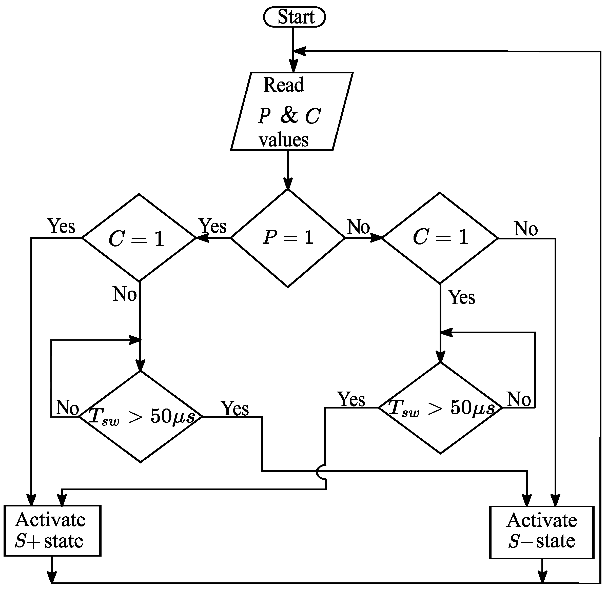
Figure 4 depicts the flow chart of the proposed logic, where the f s w is limited to 20 kHz.

2.2. Reference Correction

The current injected into the grid must be sinusoidal and should be in phase with v g to ensure unity power factor. To achieve this, the i L must be distributed evenly on either side of the i L * . It is observed in Figure 3a that the i L lies above the i L * during the positive half cycle with its lower peaks touching the i L * and thus resulting a positive DC offset. During the negative half cycle, the i L is below the i L * , with the upper peaks of the i L touching the i L * and thereby leading to a negative DC offset. These DC offsets in either half cycle cause distortion in the i L as shown in Figure 5.
To correct this DC offset in either half cycle, the i L * is corrected by (8) and (9).
i L n e w * + = i L * k
i L n e w * = i L * + k
where i L n e w * + and i L n e w * represent the positive and negative half cycles of the corrected reference ( i L n e w * ) and k is the offset correction factor.
Figure 6 demonstrates the DC offset correction over a switching cycle by correcting the reference as i L n e w * . It is seen that the i L is evenly dispersed on either side of the i L * , after the correction. Figure 7a depicts the distorted current obtained with the sinusoidal reference shown in Figure 7a. The corrected reference and the sinusoidal current thus obtained are shown in Figure 7b, respectively.
The amplitude of Δ i L p p obtained by (7) is not the same throughout the line cycle, but varies with v g as shown in Figure 8, where it is highest at zero-crossing of v g and the lowest at v g peak.
Hence, the k needed to correct the offset also varies and is half the current ripple at that instant k = Δ i L p p 2 .
From (7), the expression for the maximum amplitude of Δ i L p p is
Δ i L p p m a x = V d c 2 f s w L
The correction factor (k) corresponding to the maximum current ripple is
Δ i L p p m a x 2 = V d c 4 f s w L
The i L * is modified by (12) and (13), for the fixed offset correction of maximum current ripple as,
i L n e w * + = i L * Δ i L p p m a x 2
i L n e w * = i L * + Δ i L p p m a x 2
Figure 9 shows the i L * and the reference corrected ( i L n e w * ) by (12) and (13). The i L waveform over a line cycle with the reference corrected by a fixed offset is given in Figure 10.
The DC offset is corrected at the zero crossing while it is over-corrected at other points in the waveform. Hence, to remove the DC offset completely and to improve the i L waveform further, the i L * is modified by a variable offset given by Equations (14) and (15).
i L n e w * + = i L * Δ i L p p 2
i L n e w * = i L * + Δ i L p p 2
where Δ i L p p 2 = V d c 2 v g 2 4 f s w L V d c , is the DC offset correction factor used for variable offset correction.
The sinusoidal i L * and the reference corrected by (14) and (15) is given in Figure 11, while Figure 12 shows the i L waveform obtained with the variable offset corrected reference. As observed in Figure 12, the i L is distributed on either side of the i L * , and thus the DC offset is corrected completely.

3. Simulation Results

Table 2 lists the system parameters used in the MATLAB simulation for the implementation of the proposed logic.
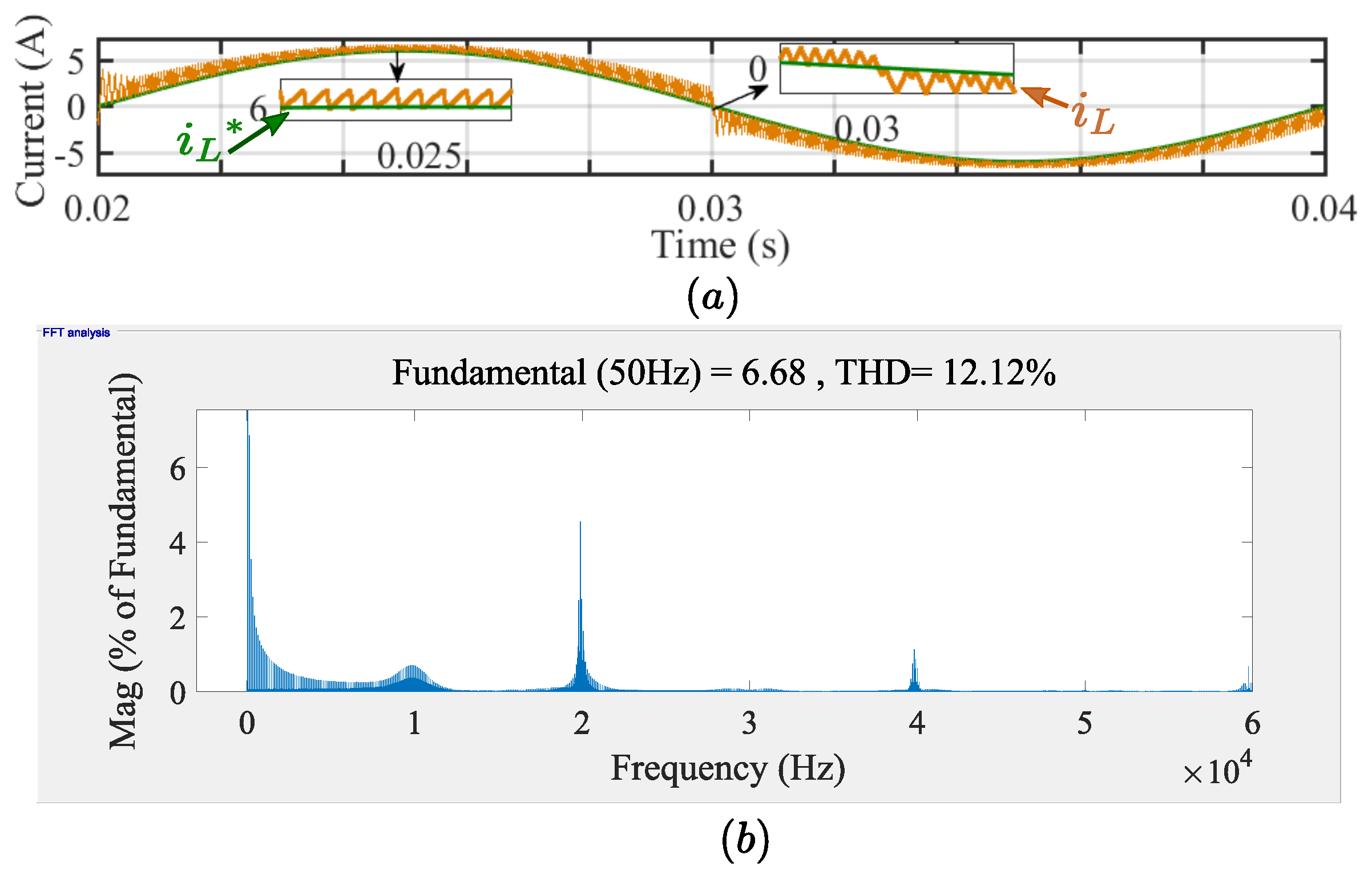
Figure 13a shows the i L waveform obtained with sinusoidal i L * , where the i L tracks the i L * well. However there is a DC offset as discussed in Section 2.2. The THD is 12.12% as shown in Figure 13b, which is more than the permissible limit of 5% as per IEEE 519, IEEE 1547, and IEC 61727 [36,37,38,39]. The following section discusses the methods to correct the DC offset and improve the THD.

3.1. Methods to Correct the DC Offset and Curb the THD

3.1.1. Modifying the Reference Current

The i L * is modified by various offset correction factors (k) as given below.
  • Fixed offset
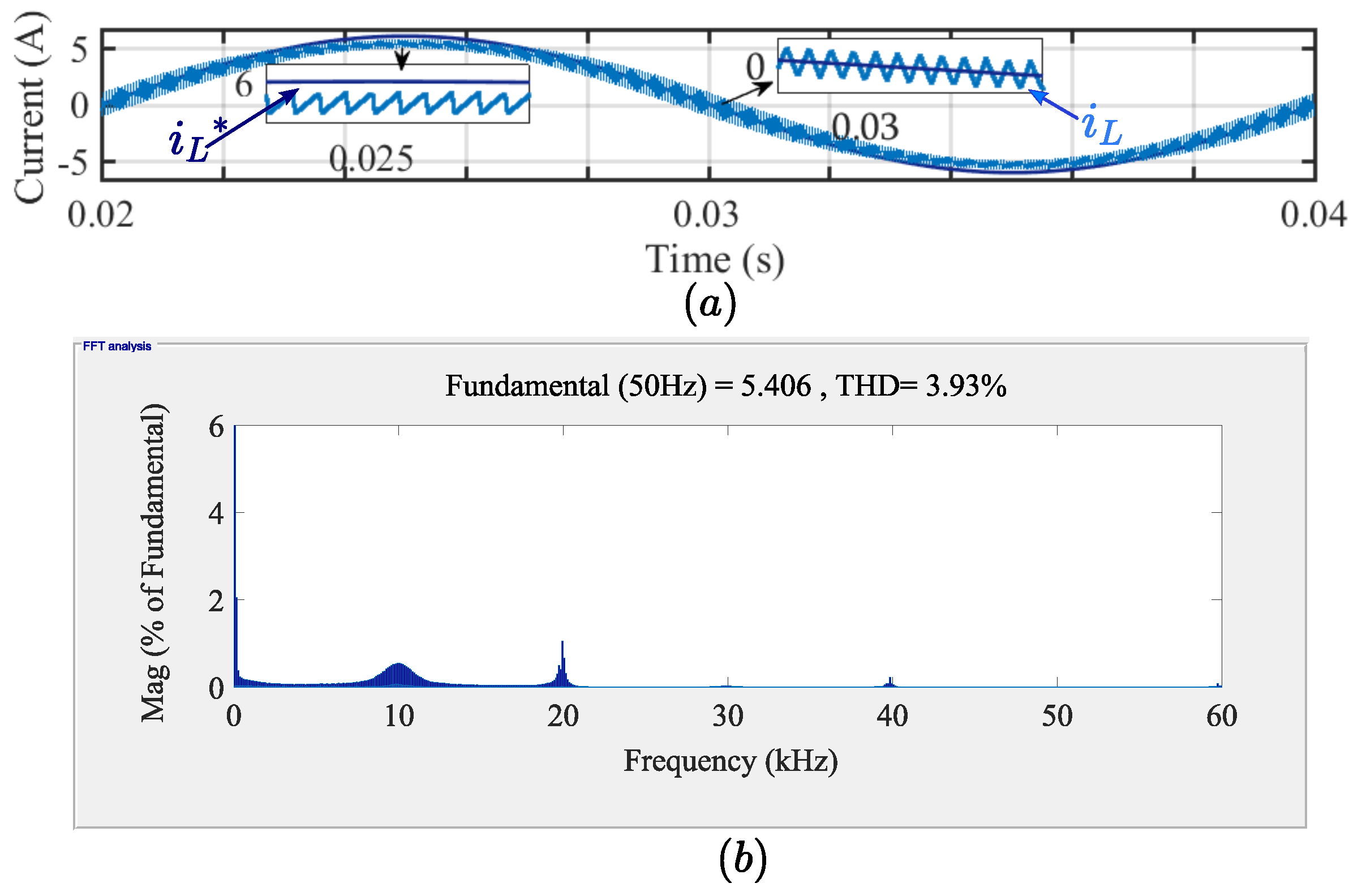
    The i L * is modified by the k, equivalent to half the maximum amplitude of inductor current ripple Δ i L p p m a x 2 given by (11) and the resulting waveform is in Figure 14a. Here the distortion at the zero-crossing is corrected completely, while the rest of the quarter-wave is over-corrected as observed in the zoomed view of the positive peak shown in Figure 14a. The THD is within the limit as shown in Figure 14b. To remove the DC offset error completely, a variable offset correction is suggested.
  • Variable Offset
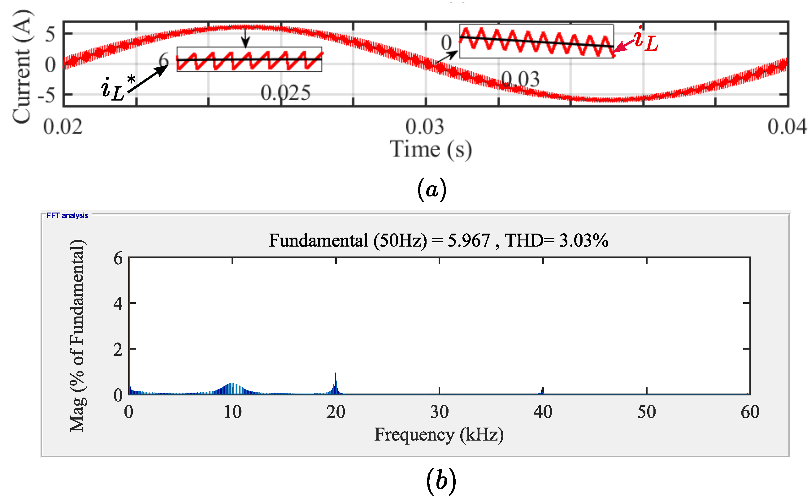
    For a given condition, the Δ i L p p in (7) varies with the instantaneous values of v g while the other parameters are kept constant. Hence, the k needed to correct the offset also varies and is half the current ripple at any instant (k = Δ i L p p / 2 ). Figure 15a shows the i L waveform corrected by the variable offset, and its frequency spectrum is given in Figure 15b. It shows that the DC offset error is corrected completely and the THD is improved even further.

3.1.2. Increasing the Inductance

Alternatively, the THD can be improved by increasing the inductance (L) without modifying the reference. Figure 16 shows the plot of THD vs L obtained by simulating the proposed logic with the sinusoidal i L * for various L values. It shows that the THD of 12.12% with the sinusoidal i L * is reduced to 5% by increasing the L from 5 mH to 13 mH at the expense of increased size and cost of the inductor.

3.2. Sensitivity Analysis

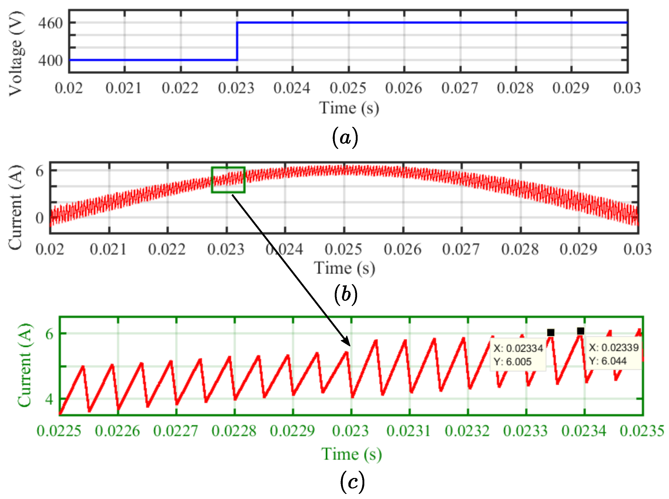
Variation in the amplitude of Δ i L p p with the supply voltage is analyzed here. Figure 17a shows the step rise in the V d c from 400 to 460 V at 0.023 s. The response of inductor current is shown in Figure 17b while its zoomed view is given in Figure 17c. It is observed that the amplitude of Δ i L p p rises instantaneously with the step rise in supply voltage; however, the switching frequency remains unchanged as indicated by the cursor values shown in Figure 17c.

3.3. Switching Frequency Analysis

To compare the switching frequency variation in the case of FB-HCC and QFFHCC, both are simulated using the parameters given in Table 2. The QFFHCC method used the variable offset corrected i L * and the hysteresis band used in the FB-HCC is equivalent to the average current ripple. Figure 18 shows the switching frequency variation in either case; where it varies between 17.8 kHz and 22.2 kHz in the FB-HCC, while the QFFHCC maintains the switching frequency constant at 20 kHz.

3.4. Transient Behavior

The FB-HCC and the QFFHCC are simulated using the parameters given in the Table 2, to analyse the transient response. A step change of 1A is given to the i L * to compare the transient response of QFFHCC with the FB-HCC, where the proposed system used the i L * modified with the variable offset. As depicted in Figure 19, the transient response of QFFHCC is equally good as that of the FB-HCC.

3.5. Comparison with a Similar Control Scheme

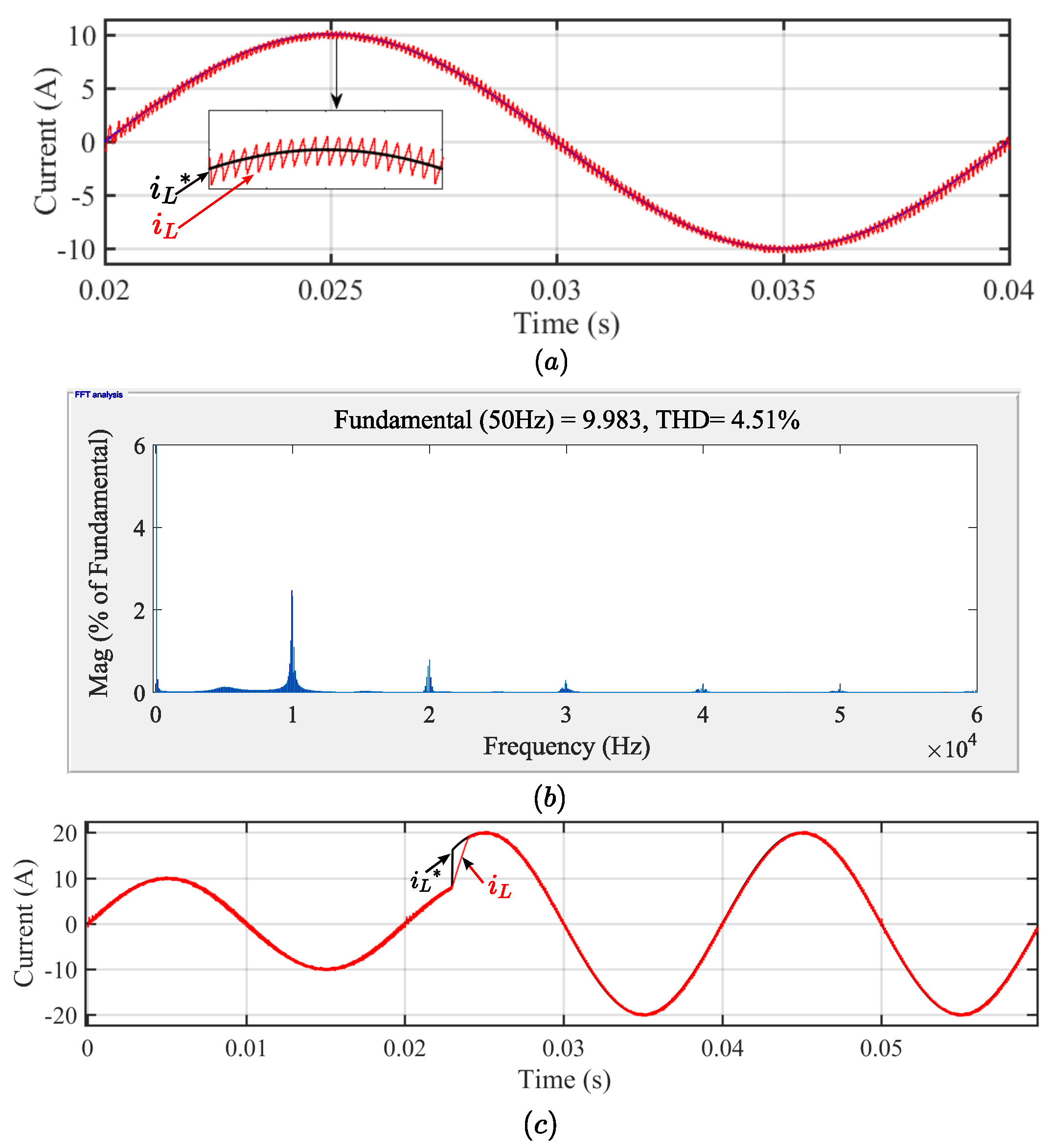
To check the superiority of the proposed method, it is compared with a similar work mentioned in [28] that implements the hysteresis current control without band and with constant switching frequency. The simulation parameters used to simulate the proposed system are the same as that given in [28] and below are the results. The Figure 20a shows the steady state inductor current waveform where the inductor current tracks the reference well. The frequency spectrum is shown in Figure 20b, where the spectrum is concentrated around 10 kHz. The constant switching frequency operation is thus guaranteed. Further, the THD observed is 4.51% which is within limits. The dynamic performance of the proposed method is analyzed by stepping the reference current from 10 A to 20 A, as in [28] and the result in Figure 20c shows that the proposed method exhibits excellent dynamic behaviour.

4. Experimental Verification

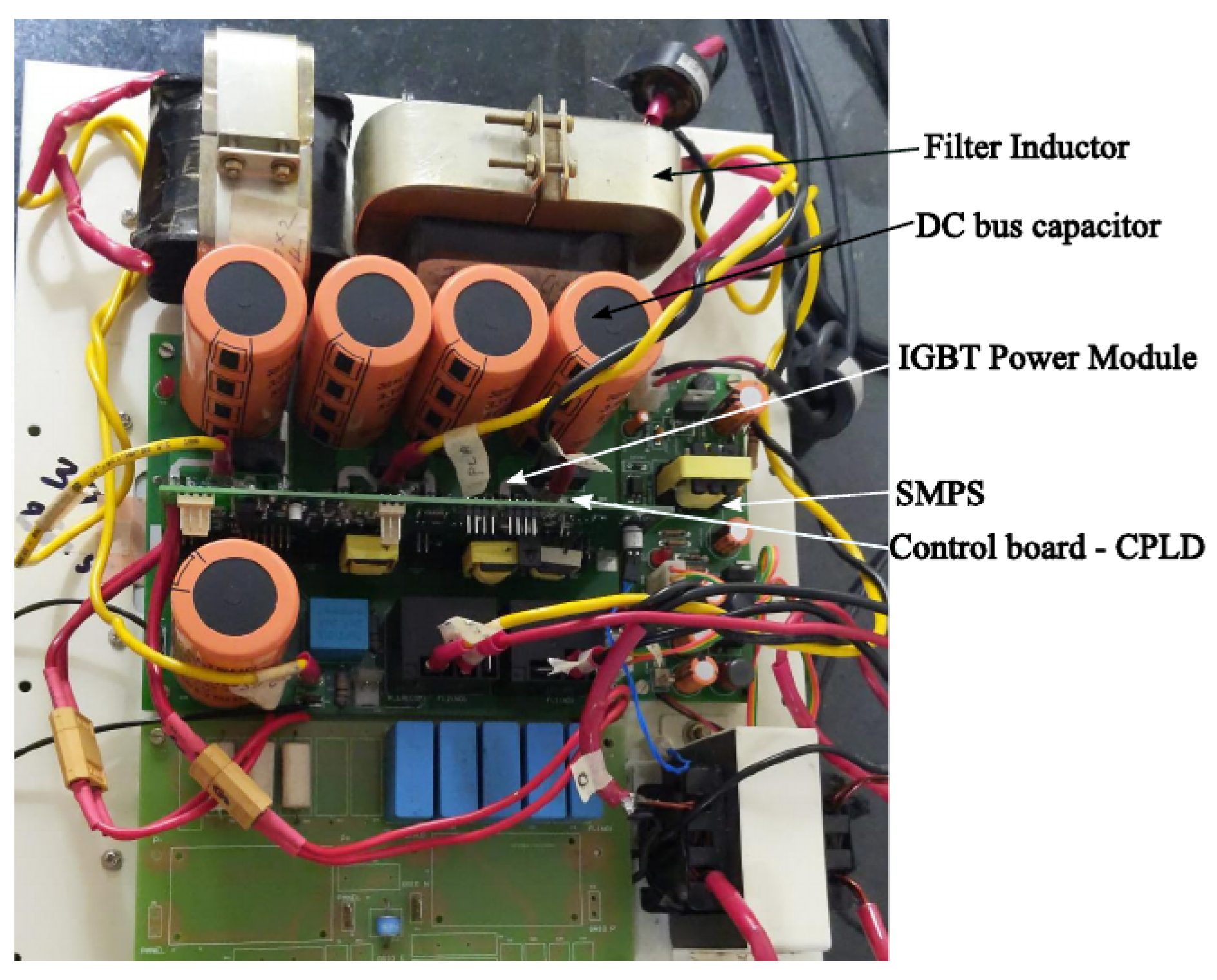
Figure 21 shows the experimental set up for validating the proposed control logic implemented in a 2 kW GI-VSI. The system parameters used for the experimental purpose are the same as that used in the MATLAB simulation. The PCB of the power circuit is designed using Altium Designer 17. It comprises four Field Stop (FS) Trench IGBTs (FGH60T65SQD) driven by optically isolated gate driver. The FS IGBT offers superior performance in switching applications with low on state voltage drop ( V C E ( s a t ) = 1.6 V) and minimal switching loss ( E t s = 327 μ J). A high precision, galvanically isolated current sensor (SI8920AC–IP) is used to feedback the i L and an external comparator is used to compare the i L * and i L . The proposed control logic is implemented on a XC9536 CPLD with advanced CMOS 5 V Fast FLASH technology. The XC9536 is a high-performance CPLD providing advanced in-system programming and test capabilities for general purpose logic integration. It comprises eight 36V18 Function Blocks, providing 800 usable gates with propagation delays of 5 ns. The CPLD dictates the switching scheme based on the nature of the i L slope.
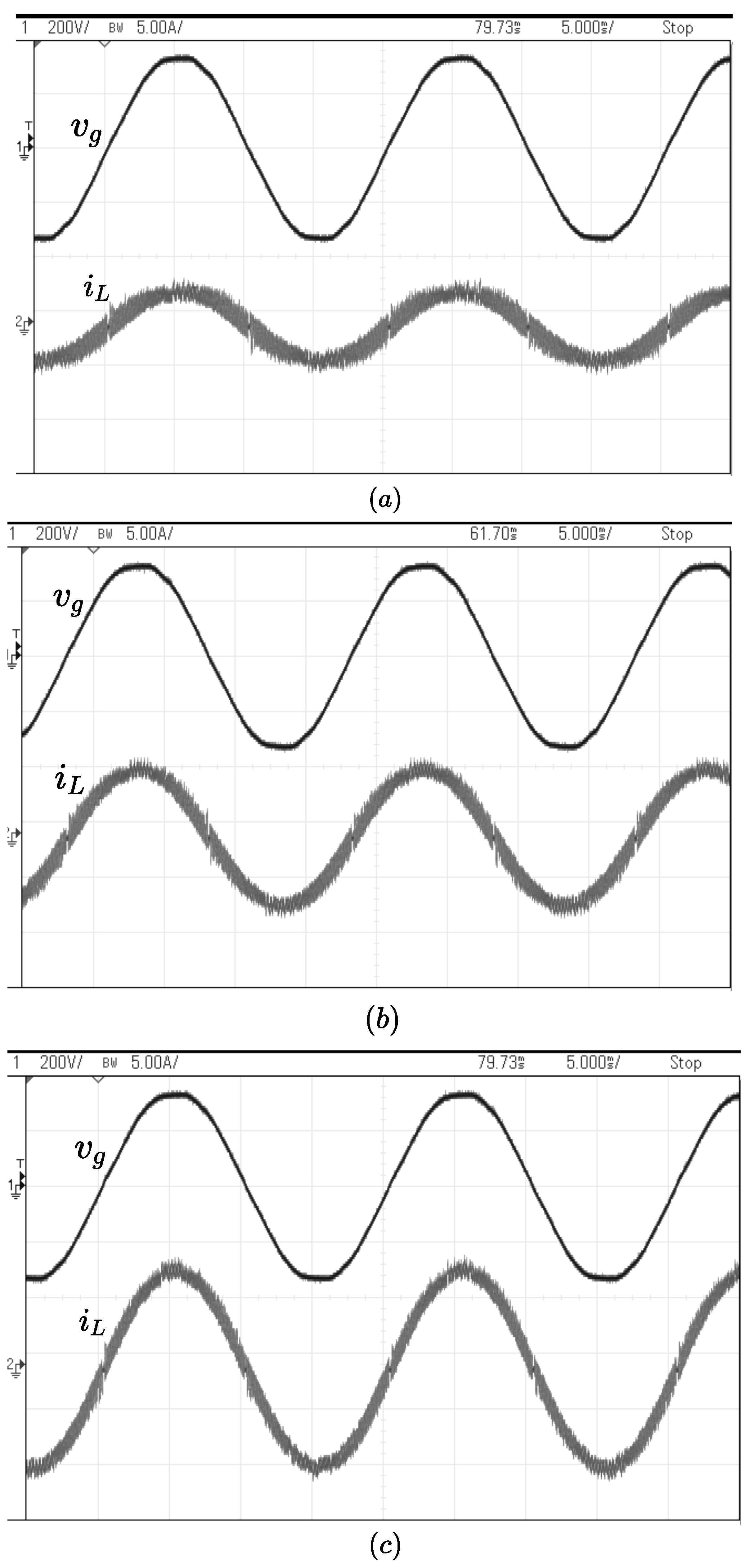
Figure 22a depicts the i L waveform for a sinusoidal i L * . The waveform has a DC offset throughout the line cycle as observed in Figure 13a. Figure 22b shows the i L waveform obtained when the i L * is modified by a correction factor which is more than the required value. To improve the i L waveform obtained in Figure 22a,b, the i L * is modified by the fixed offset of Δ i L p p m a x 2 as discussed in the Section 2.2 and the result is furnished in Figure 23. It shows that the DC offset error is corrected and the sinusoidal i L waveform, in phase with the v g , is delivered to the grid at 0.5 kW, 1 kW and 1.5 kW of power as shown in Figure 23a–c respectively.
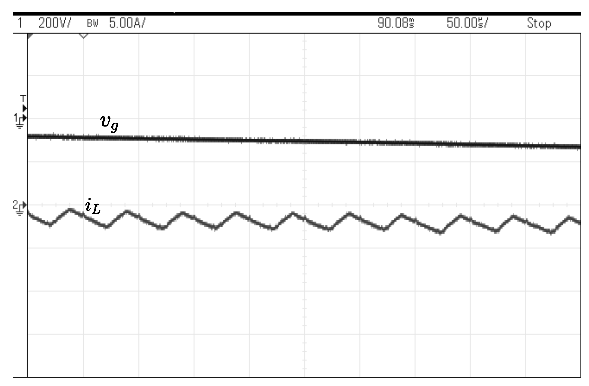
Figure 24 shows the zoomed view of Figure 23b over a switching cycle scale, where the i L maintains the T s w of 50 μ s, ensuring a constant f s w of 20 kHz. Figure 25 shows a THD of 4.04% for the i L waveform corresponding to the Figure 23b, which is acceptable as per the standards.

5. Conclusions

This paper proposes a fixed switching frequency current control strategy for a single phase full bridge GI-VSI. The proposed method ensures fixed switching frequency while retaining the benefits of conventional FB-HCC. The proposed QFFHCC method is analysed in MATLAB/Simulink. Further, its switching frequency and transient responses are compared with the conventional FB-HCC to prove its effectiveness. A 2 kW, 230 V, 50 Hz GI-VSI prototype is used for the experimental validation. The transient response of QFFHCC is similar to that of the FB-HCC, with a response time of 50 μ s. A fixed offset correction yields an experimental THD of 4.04%, which can be further enhanced using a variable offset correction. Future scope of the proposed work is to implement the QFFHCC in a three phase grid connected system and analyse its response to the grid faults.

Author Contributions

Conceptualization, M.K. and L.S.; methodology, M.K., S.E.M. and L.S.; software, D.S. and L.S.; validation, M.K., L.S. and S.E.M.; formal analysis, L.S.; investigation, L.S., S.E.M. and D.S.; resources, M.K., L.S. and B.M.J.; writing—original draft preparation, L.S.; writing—review and editing, M.K., L.S. and D.S.; visualization, M.K. and L.S.; supervision, M.K. and B.M.J.; project administration, L.S. and D.S. All authors have read and agreed to the published version of the manuscript.

Funding

This research received no external funding.

Data Availability Statement

Not applicable.

Conflicts of Interest

The authors declare no conflict of interest.

References

  1. Newell, R.; Raimi, D.; Villanueva, S.; Prest, B.; Prest, B. Global energy outlook 2021: Pathways from Paris. Resources for the Future. 2021. Available online: https://media.rff.org/documents/RFF_GEO_2021_Report_1.pdf (accessed on 1 September 2022).
  2. Eltawil, M.A.; Zhao, Z. Grid-connected photovoltaic power systems: Technical and potential problems—A review. Renew. Sustain. Energy Rev. 2010, 14, 112–129. [Google Scholar] [CrossRef]
  3. Ali Khan, M.Y.; Liu, H.; Yang, Z.; Yuan, X. A comprehensive review on grid connected photovoltaic inverters, their modulation techniques, and control strategies. Energies 2020, 13, 4185. [Google Scholar] [CrossRef]
  4. Bose, B.K.; Bose, B.K. Power Electronics and Variable Frequency Drives: Technology and Applications; IEEE Press: Piscataway, NJ, USA, 1997; Volume 996. [Google Scholar]
  5. Carrasco, J.M.; Franquelo, L.G.; Bialasiewicz, J.T.; Galván, E.; PortilloGuisado, R.C.; Prats, M.M.; León, J.I.; Moreno-Alfonso, N. Power-electronic systems for the grid integration of renewable energy sources: A survey. IEEE Trans. Ind. Electron. 2006, 53, 1002–1016. [Google Scholar] [CrossRef]
  6. Kazmierkowski, M.; Dzieniakowski, M. Review of current regulation methods for VS-PWM inverters. In Proceedings of the ISIE’93-Budapest: IEEE International Symposium on Industrial Electronics Conference Proceedings, Budapest, Hungary, 1–3 June 1993; IEEE: Piscataway, NJ, USA, 1993; pp. 448–456. [Google Scholar]
  7. Timbus, A.; Liserre, M.; Teodorescu, R.; Rodriguez, P.; Blaabjerg, F. Evaluation of current controllers for distributed power generation systems. IEEE Trans. Power Electron. 2009, 24, 654–664. [Google Scholar] [CrossRef]
  8. Kazmierkowski, M.P.; Malesani, L. Current control techniques for three-phase voltage-source PWM converters: A survey. IEEE Trans. Ind. Electron. 1998, 45, 691–703. [Google Scholar] [CrossRef]
  9. Komurcugil, H.; Ozdemir, S.; Sefa, I.; Altin, N.; Kukrer, O. Sliding-Mode Control for Single-Phase Grid-Connected LCL-Filtered VSI With Double-Band Hysteresis Scheme. IEEE Trans. Ind. Electron. 2015, 63, 864–873. [Google Scholar] [CrossRef]
  10. Kumar, N.; Saha, T.K.; Dey, J. Design and analysis of a double band hysteresis SMC for cascaded inverter-based PV system. In Proceedings of the 2016 IEEE Region 10 Conference (TENCON), Singapore, 22–25 November 2016; IEEE: Piscataway, NJ, USA, 2016; pp. 898–902. [Google Scholar]
  11. Repecho, V.; Biel, D.; Olm, J.M. A Simple Switching-Frequency-Regulated Sliding-Mode Controller for a VSI With a Full Digital Implementation. IEEE J. Emerg. Sel. Top. Power Electron. 2020, 9, 569–579. [Google Scholar] [CrossRef]
  12. Camacho, E.F.; Alba, C.B. Model Predictive Control; Springer Science & Business Media: Berlin/Heidelberg, Germany, 2013. [Google Scholar]
  13. Kouro, S.; Perez, M.A.; Rodriguez, J.; Llor, A.M.; Young, H.A. Model Predictive Control: MPC’s Role in the Evolution of Power Electronics. IEEE Ind. Electron. Mag. 2015, 9, 8–21. [Google Scholar] [CrossRef]
  14. Xia, C.; Liu, T.; Shi, T.; Song, Z. A Simplified Finite-Control-Set Model-Predictive Control for Power Converters. IEEE Trans. Ind. Inform. 2014, 10, 991–1002. [Google Scholar] [CrossRef]
  15. Le-Huy, H.; Dessaint, L.A. An adaptive current controller for PWM inverters. In Proceedings of the 1986 17th Annual IEEE Power Electronics Specialists Conference, Vancouver, BC, Canada, 23–27 June 1986; IEEE: Piscataway, NJ, USA, 1986; pp. 610–616. [Google Scholar]
  16. Rahman, K.; Khan, M.R.; Choudhury, M.; Rahman, M. Variable-band hysteresis current controllers for PWM voltage-source inverters. IEEE Trans. Power Electron. 1997, 12, 964–970. [Google Scholar] [CrossRef]
  17. Parvez, M.; Elias, M.; Rahim, N.; Osman, N. Current control techniques for three-phase grid interconnection of renewable power generation systems: A review. Sol. Energy 2016, 135, 29–42. [Google Scholar] [CrossRef]
  18. Buso, S.; Fasolo, S.; Malesani, L.; Mattavelli, P. A dead-beat adaptive hysteresis current control. IEEE Trans. Ind. Appl. 2000, 36, 1174–1180. [Google Scholar] [CrossRef]
  19. Li, Y.; Zhao, H. A Space Vector Switching Pattern Hysteresis Control Strategy in VIENNA Rectifier. IEEE Access 2020, 8, 60142–60151. [Google Scholar] [CrossRef]
  20. Bose, B.K. An adaptive hysteresis-band current control technique of a voltage-fed PWM inverter for machine drive system. IEEE Trans. Ind. Electron. 1990, 37, 402–408. [Google Scholar] [CrossRef]
  21. Malesani, L.; Tenti, P. A novel hysteresis control method for current-controlled voltage-source PWM inverters with constant modulation frequency. IEEE Trans. Ind. Appl. 1990, 26, 88–92. [Google Scholar] [CrossRef]
  22. Tripathi, A.; Sen, P.C. Comparative analysis of fixed and sinusoidal band hysteresis current controllers for voltage source inverters. IEEE Trans. Ind. Electron. 1992, 39, 63–73. [Google Scholar] [CrossRef]
  23. Malesani, L.; Mattavelli, P.; Tomasin, P. Improved constant-frequency hysteresis current control of VSI inverters with simple feedforward bandwidth prediction. IEEE Trans. Ind. Appl. 1997, 33, 1194–1202. [Google Scholar] [CrossRef] [Green Version]
  24. Tekwani, P.; Kanchan, R.; Gopakumar, K. Novel current error space phasor based hysteresis controller using parabolic bands for control of switching frequency variations. IEEE Trans. Ind. Electron. 2007, 54, 2648–2656. [Google Scholar] [CrossRef] [Green Version]
  25. Ho, C.N.M.; Cheung, V.S.; Chung, H.S.H. Constant-frequency hysteresis current control of grid-connected VSI without bandwidth control. IEEE Trans. Power Electron. 2009, 24, 2484–2495. [Google Scholar] [CrossRef]
  26. Buccella, C.; Cecati, C.; Latafat, H. Digital control of power converters—A survey. IEEE Trans. Ind. Inform. 2012, 8, 437–447. [Google Scholar] [CrossRef]
  27. Nguyen-Van, T.; Abe, R.; Tanaka, K. A digital hysteresis current control for half-bridge inverters with constrained switching frequency. Energies 2017, 10, 1610. [Google Scholar] [CrossRef] [Green Version]
  28. Wu, F.; Feng, F.; Luo, L.; Duan, J.; Sun, L. Sampling period online adjusting-based hysteresis current control without band with constant switching frequency. IEEE Trans. Ind. Electron. 2014, 62, 270–277. [Google Scholar] [CrossRef]
  29. Blaabjerg, F.; Teodorescu, R.; Liserre, M.; Timbus, A.V. Overview of control and grid synchronization for distributed power generation systems. IEEE Trans. Ind. Electron. 2006, 53, 1398–1409. [Google Scholar] [CrossRef] [Green Version]
  30. Chettibi, N.; Mellit, A. FPGA-based real time simulation and control of grid-connected photovoltaic systems. Simul. Model. Pract. Theory 2014, 43, 34–53. [Google Scholar] [CrossRef]
  31. Buso, S.; Caldognetto, T. A nonlinear wide-bandwidth digital current controller for DC–DC and DC–AC converters. IEEE Trans. Ind. Electron. 2015, 62, 7687–7695. [Google Scholar] [CrossRef]
  32. Kumar, M.; Gupta, R. Sampled-time-domain analysis of a digitally implemented current controlled inverter. IEEE Trans. Ind. Electron. 2016, 64, 217–227. [Google Scholar] [CrossRef]
  33. Al-Safi, A.; Al-Khayyat, A.; Manati, A.M.; Alhafadhi, L. Advances in fpga based pwm generation for power electronics applications: Literature review. In Proceedings of the 2020 11th IEEE Annual Information Technology, Electronics and Mobile Communication Conference (IEMCON), Online, 4–7 November 2020; IEEE: Piscataway, NJ, USA, 2020; pp. 252–259. [Google Scholar]
  34. Sankar, D.; Syamala, L.; Chembathu Ayyappan, B.; Kallarackal, M. FPGA-Based Cost-Effective and Resource Optimized Solution of Predictive Direct Current Control for Power Converters. Energies 2021, 14, 7669. [Google Scholar] [CrossRef]
  35. Nguyen, V.T.; Dam, M.T.; So, J.; Lee, J.G. Immunity Characterization of FPGA I/Os for Fault-Tolerant Circuit Designs against EMI. Adv. Electr. Comput. Eng. 2019, 19, 37–44. [Google Scholar] [CrossRef]
  36. Dartawan, K.; Najafabadi, A.M. Case study: Applying IEEE Std. 519-2014 for harmonic distortion analysis of a 180 MW solar farm. In Proceedings of the 2017 IEEE Power & Energy Society General Meeting, Chicago, IL, USA, 16–20 July 2017; IEEE: Piscataway, NJ, USA, 2017; pp. 1–5. [Google Scholar]
  37. Photovoltaics, D.G.; Storage, E. IEEE 1547–2018—IEEE Standard for Interconnection and Interoperability of Distributed Energy Resources with Associated Electric Power Systems Interfaces—Redline. 2018. Available online: https://ieeexplore.ieee.org/document/8365917547–2018 (accessed on 1 September 2022).
  38. International Electrotechnical Commission. IEC 61727-2004 Photovoltaic (PV) Systems: Characteristics of the U-tility Interface. 2007. Available online: https://global.ihs.com/doc_detail.cfm?item_s_key=00285429#referenced-documents (accessed on 1 September 2022).
  39. Arranz-Gimon, A.; Zorita-Lamadrid, A.; Morinigo-Sotelo, D.; Duque-Perez, O. A review of total harmonic distortion factors for the measurement of harmonic and interharmonic pollution in modern power systems. Energies 2021, 14, 6467. [Google Scholar] [CrossRef]
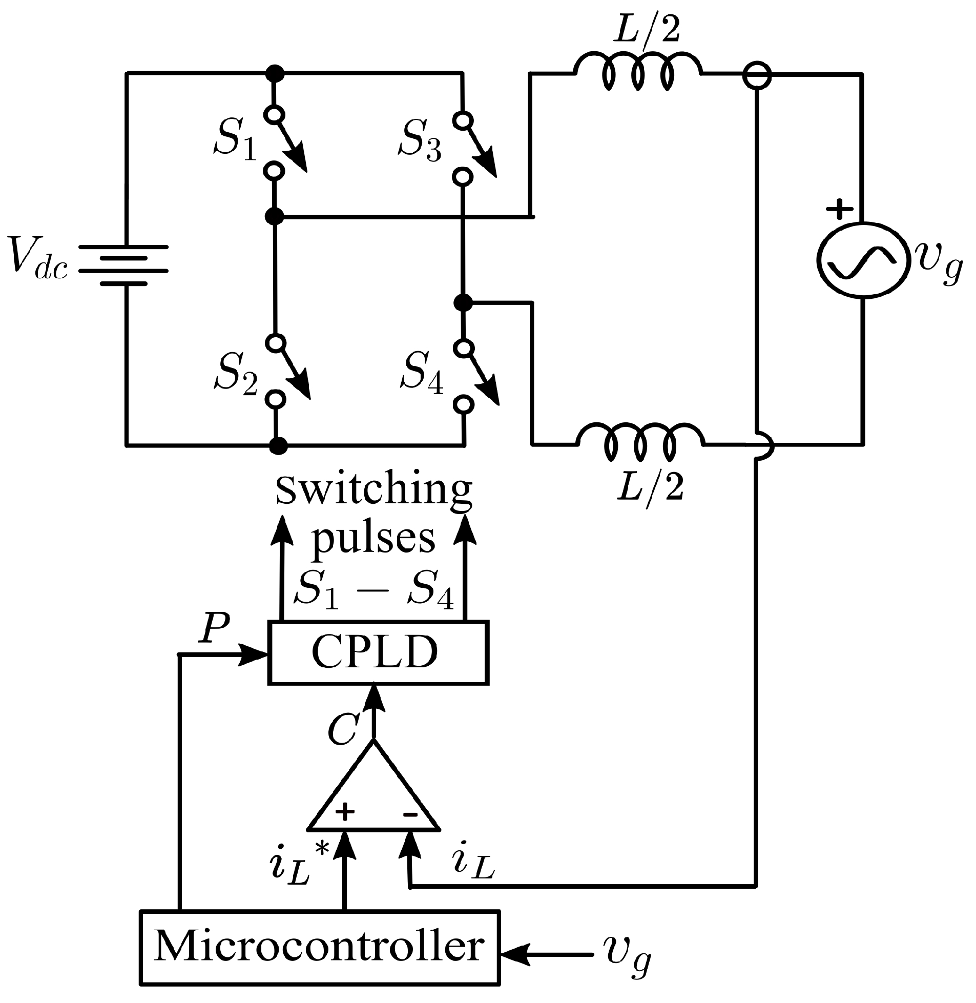
Figure 1. Schematic of the single phase full bridge grid integrated inverter with the proposed logic.
Energies 15 08112 g001
Figure 2. The switching states (a) S + and (b) S during the positive half cycle.
Energies 15 08112 g002
Figure 3. Sketch of inductor current over a switching cycle (a) Positive Half Cycle. (b) Negative Half Cycle.
Energies 15 08112 g003
Figure 4. Flowchart of the proposed logic implemented in CPLD.
Energies 15 08112 g004
Figure 5. Sketch of inductor current over a line cycle with the sinusoidal reference current.
Energies 15 08112 g005
Figure 6. Pictorial representation of reference correction over a switching cycle (a) Positive half cycle. (b) Negative half cycle.
Energies 15 08112 g006
Figure 7. Sketch of inductor current over a line cycle with (a) Sinusoidal reference. (b) Corrected reference.
Energies 15 08112 g007
Figure 8. Variation in the amplitude of the inductor current ripple with the grid voltage.
Energies 15 08112 g008
Figure 9. Sinusoidal reference and the reference corrected by fixed offset.
Energies 15 08112 g009
Figure 10. Inductor current obtained with the fixed offset corrected reference.
Energies 15 08112 g010
Figure 11. Sketch of sinusoidal reference and the reference corrected by variable offset.
Energies 15 08112 g011
Figure 12. Sketch of Inductor current obtained with the variable offset corrected reference.
Energies 15 08112 g012
Figure 13. (a) Inductor current waveform obtained with the Sinusoidal reference. (b) Frequency spectrum of inductor current obtained with the Sinusoidal reference.
Energies 15 08112 g013
Figure 14. (a) Inductor current waveform obtained with fixed offset correction (k = Δ i L p p m a x 2 ). (b) Frequency spectrum of inductor current obtained with fixed offset correction.
Energies 15 08112 g014
Figure 15. (a) Inductor current waveform obtained with variable offset correction (k = Δ i L p p 2 ). (b) Frequency spectrum of inductor current obtained with variable offset correction.
Energies 15 08112 g015
Figure 16. THD vs. Inductance plot.
Energies 15 08112 g016
Figure 17. (a) Step rise in the supply voltage. (b) Inductor current waveform over a half cycle. (c) Inductor current waveform zoomed around the step change.
Energies 15 08112 g017
Figure 18. Comparison of switching frequencies in the case of FB-HCC and the QFFHCC.
Energies 15 08112 g018
Figure 19. Comparison of transient response in the case of FB-HCC and the QFFHCC.
Energies 15 08112 g019
Figure 20. Waveforms obtained by simulating the proposed method with the parameters in [28]. (a) Steady state performance of the proposed method. (b) Frequency spectrum. (c) Dynamic response.
Energies 15 08112 g020
Figure 21. Experimental set up: 2 kW GI-VSI prototype.
Energies 15 08112 g021
Figure 22. Inductor current obtained with (a) Sinusoidal i L * (b) Over-corrected i L * .
Energies 15 08112 g022
Figure 23. Synchronised operation of single phase GI-VSI delivering (a) 0.5 kW (b) 1 kW (c) 1.5 kW.
Energies 15 08112 g023
Figure 24. Zoomed view of inductor current.
Energies 15 08112 g024
Figure 25. Harmonic spectrum of inductor current for the proposed method.
Energies 15 08112 g025
Table 1. Comparison of advanced control strategies with the proposed method.
MPCSMCQFFHCC
(1) Non-linear controller
(2) No modulation needed
(3) Handle system constraints
in an intuitive way
(4) Can include non-conventional
control objectives
(1) Robustness to parameter
variations
(2) Fast transient response
(3) Reduction in system order
(1) Non-linear controller
(2) Easy to implement
(3) No modulators are used
(4) Very fast transient response
(5) Robust
(6) Offers fixed switching
frequency
(7) Works well with advanced
controllers like
FPGA/CPLD
(1) Variable switching
frequency
(2) High computational burden
(1) Chattering effect
(2) Variable switching
frequency
(1) Performance depends on the
controller used
(2) Current feedback is needed
Table 2. System Parameters.
ParameterValue
V d c 400 V
f o 50 Hz
v g r m s 230 V
f s w 20 kHz
L5 mH
i L * p e a k 6 A
Publisher’s Note: MDPI stays neutral with regard to jurisdictional claims in published maps and institutional affiliations.