Article

Analysis of Surface Texturing of Silicon with Surface Regular Microstructure Using C Method

by
Hamid Reza Dehghanpour
1,
Parviz Parvin
2,*,
Seyedeh Zahra Mortazavi
3,
Ali Reyhani
3,
Amin Chegenizadeh
2 and
Mohammadreza Aghaei
4,5,*
1
Department of Physics, Tafresh University, Tafresh 39518-79611, Iran
2
Energy Engineering and Physics Department, Amirkabir University of Technology, Tehran 15119-43943, Iran
3
Department of Physics, Imam Khomeini International University, Qazvin 34149-16818, Iran
4
Department of Ocean Operations and Civil Engineering, Norwegian University of Science and Technology (NTNU), 6009 Alesund, Norway
5
Department of Sustainable Systems Engineering (INATECH), University of Freiburg, 79110 Freiburg, Germany
*
Authors to whom correspondence should be addressed.
Energies 2022, 15(20), 7540; https://doi.org/10.3390/en15207540
Submission received: 6 September 2022 / Revised: 4 October 2022 / Accepted: 10 October 2022 / Published: 13 October 2022
(This article belongs to the Section D3: Nanoenergy)

Abstract

:
Silicon, as the most abundant element in the earth’s crust and the most common material used in electronic and optical equipment, has attracted the attention of many individuals to change the properties of this material, improving its electronic and optical properties. One of these efforts relies on the reduction of surface reflection by making use of different methods. However, among them, the use of lasers in creating surface microstructures has been of special importance because there is no need for masks and other additional materials. In this work, a theoretical method is utilized to analyze these textures with the theorem of diffraction grating on a micrometer scale. The surface reflection of the microstructure created by excimer laser exposure on a silicon surface is simulated. The theoretical Coordinate transformation method (C method) gives out notable results against the experimental records by approximating triangular and trapezoidal microstructures. The model is useful for predicting the reflective response of the modified microstructural morphology. One of the main applications is the texturing of the solar cell front faces to enhance their efficiency, mainly due to photon trapping.

1. Introduction

The exponential growth of the human population elevates the need for energy. The limitation of non-renewable energy sources, such as fossil fuels, increases the global demand for the use of renewable and accessible energy sources. Solar energy is one of the freely renewable sources that is available throughout the planet and its surroundings, i.e., the space around the earth and outside its atmosphere. Due to the novelty of the field of solar equipment, modernity does not mean the number of years of presence of this equipment in human life and industry, but rather the efficiency of equipment that the values obtained for their efficiency is still far from the desired values. The need to increase the efficiency of these solar panels is obviously seen, and a 0.1% increase in the efficiency of a particular type of solar cell is very significant and commendable. Among solar cells, silicon cells are of great importance in order to increase their efficiency due to their age, reasonable price and low efficiency. Among the light losses for a flat silicon cell is the reflection of 30% of the incoming light, which results in a loss of a fraction of the convertible optical power to the useful electrical energy. However, unlike some losses for a solar cell that are unavoidable and irreparable, there are ways to reduce surface reflection. One of the methods relies on the reduction of spectral reflection of the Si cell surface by making use of anti-reflective coatings or inducing microstructuring on the Si surface. However, most of these methods are effective for a certain spectral range and do not cover the entire optical spectrum. Another method that reduces reflection over a wide range of wavelengths is to create regular, alternating structures on the surface of silicon or any other material. This increases the number of collisions of incident light to the surface, as in each collision, a fraction of the incident light is reflected. In terms of comparison with a flat surface, consider that 30% of the reflected light hits the surface again. This absorbs another 21% of this 30%, leading to a final reflection of 9%. There are many methods for creating alternating structures on the surface, among which the method of creating microstructures using laser shots owns its own advantages against the other methods because it does not require additional materials and complicated processes. Recently, surface texturing using laser radiation has become a common and well-known method [1,2,3]. The laser irradiation creates some regular self-organizing microstructures on the surface, indicating significant optical/electrical properties. One of the useful optical properties of the microstructures is the reduction of the surface reflection for a large spectral range [4,5,6,7,8].
Observations of laser light with different wavelengths on the surface of materials in different gaseous environments have been reported repeatedly in previous works [9,10,11,12,13]. The microstructures with dimensions of several tens of micrometers are created by excimer laser light with nanoseconds duration, which reduces the surface reflection to less than 10% over a spectral range of 200–3000 nm. It is worth noting that silicon whose surface is modified is known as black silicon because of its absorption over a wide range of wavelengths and the spectral reflections of 10%.
The reflectance of these microstructures has been measured, and the numerical methods used to predict the spectral reflectance of periodic structures using the grating theory. The approximation of surface microstructures to 2D alternating triangular structures has been studied [14]. The reflection of the microstructures is obtained using method C. Moreover, the creation of regular microstructures by the ArF excimer laser on the polymer surface of the solar cell attests to a decrease in spectral reflection alongside the flattening of the spectral reflection. This causes to enhance the efficiency of the solar cell by ~1% [15,16,17,18,19]. Moreover, the ZnO nanowires contribute to enhancing solar cell efficiencies due to UV-blue spectral downshifting [20,21].
To the best of our knowledge, there is no similar report on the modeling of the microstructures, such as trapezoidal/triangular skin morphology and the alternating microstructures obtained from laser irradiation, analyzing them with numerical methods. In this work, the presence of ripples on the surface of conical structures caused by UV laser exposure has been investigated for the first time. Needle structures whose dimensions of the periodicity are in the range of several tens of nanometers and whose height is ~30 times larger than their periodicity have also been reported here.

2. Materials and Methods

In order to study microstructures approximately equal to the wavelength of the incident light, it is necessary to use the diffraction gratings model. The diffraction grating is an arrangement of optical elements that, when placed next to each other, act to diffract the descending electromagnetic waves [22]. The grating elements diffract light of a specific wavelength into discrete order, each of which corresponds to a different direction that travels outside the grating. Our goal is to examine a diffraction grating in which light transmits in addition to its reflection.
Transmission gratings are a type of grating showing periodic texturing in two non-aligned directions [23]. Since 1970, transmission diffraction grating has found many applications, such as solar absorbers, beam splitters, non-reflective surfaces, and optical filters, and it is a vital element in optical spectrometers. Many precise numerical methods are available for implementing the transmission grating response, including the differential method [24,25,26], integral method [27], iterative method [28,29], C method [12,30,31], Fourier modal method (FMM) [32,33,34], Fourier-Ryleigh method [35,36] and border changing method [37,38] and other similar methods have been developed so far. All the methods above are time-consuming that require a lot of memory to run. In precision theories, the cost of calculations is proportional to the third power of the number of unknowns. Full details of the experimental work leading to the creation of the regular microstructure simulated in this work are provided in Ref. [9], and the theoretical analysis is given in Ref. [10]. We have specifically simulated one of the regular microstructures created on the silicon surface by excimer laser irradiation. In the experimental part, according to Ref. [9], we used a Lambda Physik LPX200 ArF excimer laser at 193 nm to create the skin microstructures on silicon (single crystal n-type <111> wafers, resistivity of 0.01 Ω cm, Virginia Semiconductor Inc. Frederickburg, VA, USA) and a Phillips SEM model XL30 to study the surface morphology. The method used to study the microstructures obtained from the experimental results [9,10] is the C method which is described in detail in the continuation of this work.

2.1. Method C

The C method was born in the 1980s due to the need to accurately solve diffraction problems on surfaces with periodic pores [39,40,41]. Recently, this method has been used as a powerful modeling tool for three-dimensional photonic structures [42], complex geometries of diffraction gratings [43] and error calibration [44]. The main difficulty of such issues was the adaptation of border conditions. It is clear that any method for solving Maxwell equations is the most efficient where it can fit the geometry of the problem [45,46].
In this work, we refer to two articles [19,39] that analyze textured surfaces using the C method. To explain this method carefully, a periodic porous surface is presumed, without any change in the z direction, which separates a couple of homogeneous environments with similar properties and as shown in Figure 1a [39]. The periodicity and depth of the grating are represented by d and h. The grating surface function, a (x), is a general function as long as it is a continuous and single value. The incident angle θ and the incident wave vector are assumed in the xoy plane. For simplicity, only the TM polarization mode is considered. In order to determine the results for TE polarization, it is sufficient to exchange E↔H, ε 0 μ 0 , ε μ . In this method, only one coordinate system, i.e., the Cartesian coordinate system, is used, and the time dependence is adopted as exp (−iωt).
To express the grating problem mathematically, a little preparation is needed. Figure 1b depicts 2 dashed lines representing the maximum and minimum values of the function a (x). These lines divide the space into 3 parts: D1, D0 and D2. In addition, these areas are marked using the 2 halves of the upper and lower spaces, y = a (x). Starting from Maxwell equations, we can easily write the following wave equation [35]:
( 2 x 2 + 2 y 2 + k 0 2 μ ε ) F = 0
The field can be expressed in terms of Ryleigh expansion [36], which is the sum of flat waves with different directions created by the periodicity of the grating in regions D1 and D2. These flat waves are named diffraction orders [18]:
F 1 ( x , y ) = exp [ j ( α 0 x + β 0 ( 1 ) y ) ] + m A m ( 1 ) exp [ j ( α m x β m ( 1 ) y ) ] , in D 1
F 2 ( x , y ) = m A m ( 2 ) exp [ j ( α m x + β m ( 2 ) y ) ] , in D 2
When F is an electric or magnetic field, and the subscripts 1 and 2 correspond to the regions in which this answer is valid. The first part of the expansion is related to the incident wave, whose amplitude is assumed to be unified. The flat waves within the sigma sign propagate around the surface of the diffraction grating. The amount of propagation constants is also calculated from the following equations [18]:
α m = n 1 k 0 sin θ + m 2 π D
β m ( p ) = ( n p 2 k 0 2 α m 2 ) 1 / 2 ,   I m ( β m ( p ) ) > 0 ,   p = 1 ,   5
Only a small number of propagation constants β m ( p ) related to the reflected waves are real numbers, and the flat waves corresponding to these constants propagate without attenuation, in which case the propagation angle θ m is determined from the following relation [18]:
sin θ m = sin θ + m 2 π D n 1 k 0
The other residual β m ( p ) constants are complex, and the waves corresponding to these constants are attenuated in the positive direction of the y-axis. These waves are unstable and are not found in the field away from the grating, and do not participate in the reflected power. If n2 is complex, all the flat waves propagating into the insulation, transmitted orders, will be unstable. Otherwise, a limited number of orders will participate in the long-distance transmitted field as the reflected field [18]. The zero-order part (m = 0) is propagated in both media based on what the laws of reflection and Snell refraction specify for smooth surfaces. The conditions in which the reflection orders participate in the far field due to the reflection for the zero angle of incidence (θ = 0) are given as follows [18]:
n 1 k 0 2 α m 2 > 0   m 2 π D < n 1 k 0 m < n 1 D λ
Therefore, the larger the grating period, the greater the number of reflection orders. For wavelengths larger than the grating period, there is only zero-order, propagating in a direction proportional to the smooth surface. In order to determine the diffraction amplitudes A m ( p ) , the continuity of tangential fields along the surface must be considered. Therefore, it is necessary to connect the provided fields in D1 and D2. However, the accuracy of Ryleigh expansion, Equations (2) and (3), is limited to areas where the refractive index is constant [36]. That is why the poor convergence of methods takes place based on the generalization of the equation to Ryleigh expansion in the D0 region. In fact, the convergence of such methods can be achieved in favor of shallow gratings [36,40]. Because the scattered field at y = ± ∞ must be finite and outgoing, then A m ( 2 ) + = 0 is zero for all m and A m ( 1 ) = 0 in favor of m ≠ 0. For simplicity, A 0 ( 1 ) = 1 , equivalent to unity is the amplitude of the incident wave in solving the problem by the Ryleigh method, where A m ( 1 ) + = A m ( 1 ) and A m ( 2 ) = A m ( 2 ) are considered. Then, in order to determine the value of these unknown coefficients, the regions D1 and D2 must be connected to each other. However, according to previous explanations, Ryleigh expansion in the D0 area is generally invalid. Thus, the grating problem involves the solution of the Helmholtz equation in D1 and D2 regions under boundary conditions at infinity and along y = a (x) [39].
The references [18,39] have stated the mathematical basis and modeling for the surface reflection of the regular structure with general geometries based on the theory of gratings, while this work benefits the provided tool for the specific morphology of the microstructure created by laser on the silicon surface. The models of the isosceles triangle, trapezoid and hybrid schemes are proposed based on the direct investigation of the surface morphology of textured silicon and are exclusively dedicated to these experimental results. Using the mathematical model and the results predicted by this model are compared with those experimental results that lucidly attest to a good agreement as another success.

2.2. MATLAB Programming

Because we have an eigenvalue problem and the use of matrix in the C method, MATLAB software with a great ability to solve matrix problems is chosen for coding. During the coding, in order to reduce the calculation time, changes are made in some parts of the programming code to optimize the calculation time so that, finally, the optimal code is prepared. The way to run the programmed code is that the whole code is executed once for each wavelength, and all the calculations are done. Then the result for each wavelength is stored in a matrix. After completing the calculations for all the selected wavelengths, the result is drawn as the amount of reflection (in percent) by wavelength in a graph.
The convergence and consumption time of this code depends on the type of grating surface function. So for sinusoidal grating, the result is reached with less time and fewer approximations. However, for triangular/trapezoidal grating, more approximations and more time are needed. In this method, the more the number of matrix approximations, the closer the solution is to the real value, and more time is required for the result.
The ray optics method is also coded using Fresnel’s relations and other mathematical relations connected to them. The results of this coding are also used.

2.3. Simulation of Periodic Microstructures

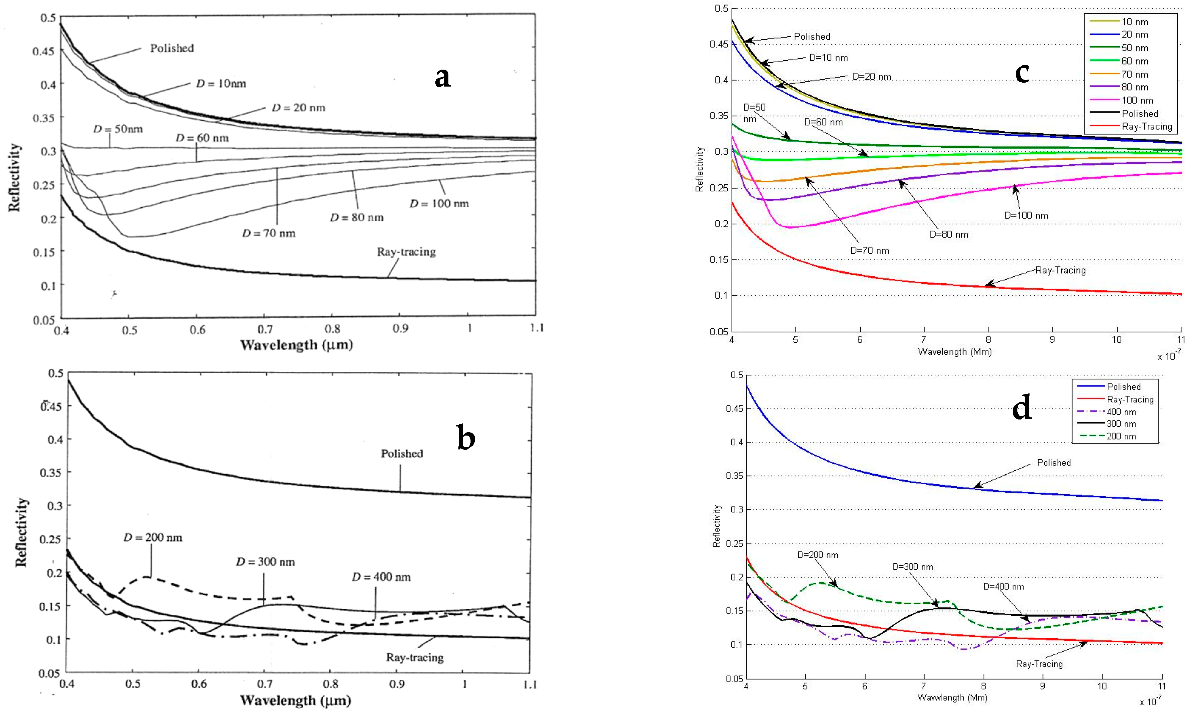
Due to the eigenvalue problem and the use of matrices in the C method, MATLAB software is selected to code this model, which benefits a great ability to solve matrix problems. The operation of the programmed code is carried out for each wavelength, and all calculations are performed, then the result is stored in a matrix for each wavelength. After completing the calculations for all selected wavelengths, the result is plotted as a reflection rate (in percent) in terms of wavelength. The convergence and execution time of this code depends on the type of grating surface function, such that for a sinusoidal grating with less time and a number of approximations, the result is well obtained. However, the triangular grating requires more approximations and certainly takes more time. In this method, the greater the number of matrix approximations, the closer the answer to the actual value. Using Fresnel relations and precise mathematical calculations, the ray optics are coded, and the results of this coding have been recorded accordingly. After fulfilling the previous step, when the C method is converted to MATLAB programming, it is essential to check the validation of the code. To do this task, some numerical examples that are available in the references [18,39].
According to Figure 2a–d, the accuracy of the programming code is fully verified. According to these figures, our code is well in agreement with those of reference [18] by making use of the C method.
After successfully implementing the C method and also checking the accuracy of this code, then an attempt was made to simulate the structures discussed by the references [9,10]. In the following discussion, we will fully describe the characteristics of this grating-like structure from references [9,10]. Microstructures with an average height of 100 μm and a base (periodicity) of 14 μm are considered for the simulation.

3. Results and Discussion

3.1. Triangular Model

After estimating the size of microstructures using [9,10] considering the average height of 100 μm and the divergence of the C method in the deep gratings, it is forced to simulate the aspect ratio of these textures. In such a way, we set the aspect ratios of these microstructures in the simulation such that the ratio is equal to 100/14, where the C method does not diverge, and the amount of reflection is obtained. According to the mentioned explanations, the following results give out as follows.
Three of the available average heights are selected with values of 64, 70 and 100 μm with a fixed base of 14 μm as an exemplary run. For all three samples for simulation, the base of 14 nm and the aspect ratios of 64/14, 70/14 and 100/14 are chosen, as shown in Figure 3a. Figure 3b illustrates the output of the simulation using MATLAB. Despite the results given in this figure being somewhat acceptable, however, it is not close to real texturing. The expected results are close to the experimental graphs. Therefore, efforts were made to simulate surface rippling that is similar in size to the real microstructures in order to obtain better results, some of which are mentioned below.
The size distribution of the structures, as well as the variability of the separation distance between them, are taken into account as major parameters to induce these structures to be placed next to each other in such a way as to form a structure similar to Figure 4a. This prompted us to perform the simulation based on Figure 4b in order to get as close as possible to the properties of the real structures. Figure 4c displays the spectral response in favor of triangular microstructures with a periodicity of 30 μm and a height several times smaller than the experimental structures. This corresponds to the experimental graphs in terms of the reflection diagram, which provides a completely flat profile for a wide spectral range. For further investigation, assuming that the coefficient of y1 and y2 equations, as shown in Figure 4b, take a value of two, which increases the height of the microstructures in the case where the period of the structure invariant and the simulation runs for the some texturing given in Figure 4c. The results are shown in Figure 5a. The reflectance decreases in terms of the height of the microstructures, and the spectral reflection is less than 10%, ranging from wavelengths of 200–3000 nm. To better compare, Figure 5b depicts two states of 25 and 30 μm of these two structures in a single frame. The structures introduced in Figure 4a,b exhibit a significant number according to the SEM images of the experimental structure, demonstrating a behavior very close to the experimental findings. This structure can play a role in the final surface reflection diagram, emphasizing a combination of the microstructures of interest that gives out an optimal condition.
The surfaces related to triangular structures are not smooth, and ripples are observed on their surface. The effect of these ripples is further investigated by assuming the surface of triangular structures to be uneven. According to Figure 6, for a sample with 20 ripples of 200 nm height, the surface is less reflective than the structure with a smooth surface. However, for a sample with a surface of seven ripples with 100 nm height, then the reflection rate is almost equal to that of the original sample. Hence, the unevenness of the morphology formed by excimer laser irradiation affects the spectral reflection and the larger the number of ripples, the lower the surface spectral reflectance.
According to the experimental diagram that shows the height distribution of texturing formed on the silicon surface [9], the triangular microstructures with height distribution, as shown in Figure 7a, are also simulated to investigate the effect of this phenomenon. Figure 7a plots the general microstructure for the simulation. According to Figure 7b, the simulation results of the size distribution and height of conical structures due to excimer laser radiation elevate the microstructure’s surface reflection of variable size compared to an integrated texturing of the same size. In Figure 7b, two microstructures with a base of 2900 nm and heights of 2510 and 7260 nm are selected as integrated microstructures, and two series of 11 triangles together are considered to study the effect of height distribution.
To investigate the effect of the height elevation with a fixed periodicity, several microstructures with a periodicity of 100 nm and variable heights have been examined, and acceptable results were obtained. In fact, those are isosceles triangles with leg angles ranging from 30° to 87°. It is worth noting that the experimental structures obtained after the excimer laser exposure, assuming periodicity 14 μm and 100 μm in height, are proportional to the isosceles triangles with a leg angle of approximately 86°. The study of these structures is useful in the prediction of the behavior of real microstructures.
According to Figure 8, the spectral reflection for a given microstructure with a leg angle of 30°–87° and a period of 100 nm does not exceed 10%. This corresponds to the experimental spectral reflection [9], and the diagrams are almost much smoother for a wide range of wavelengths.

3.2. Trapezoid Model

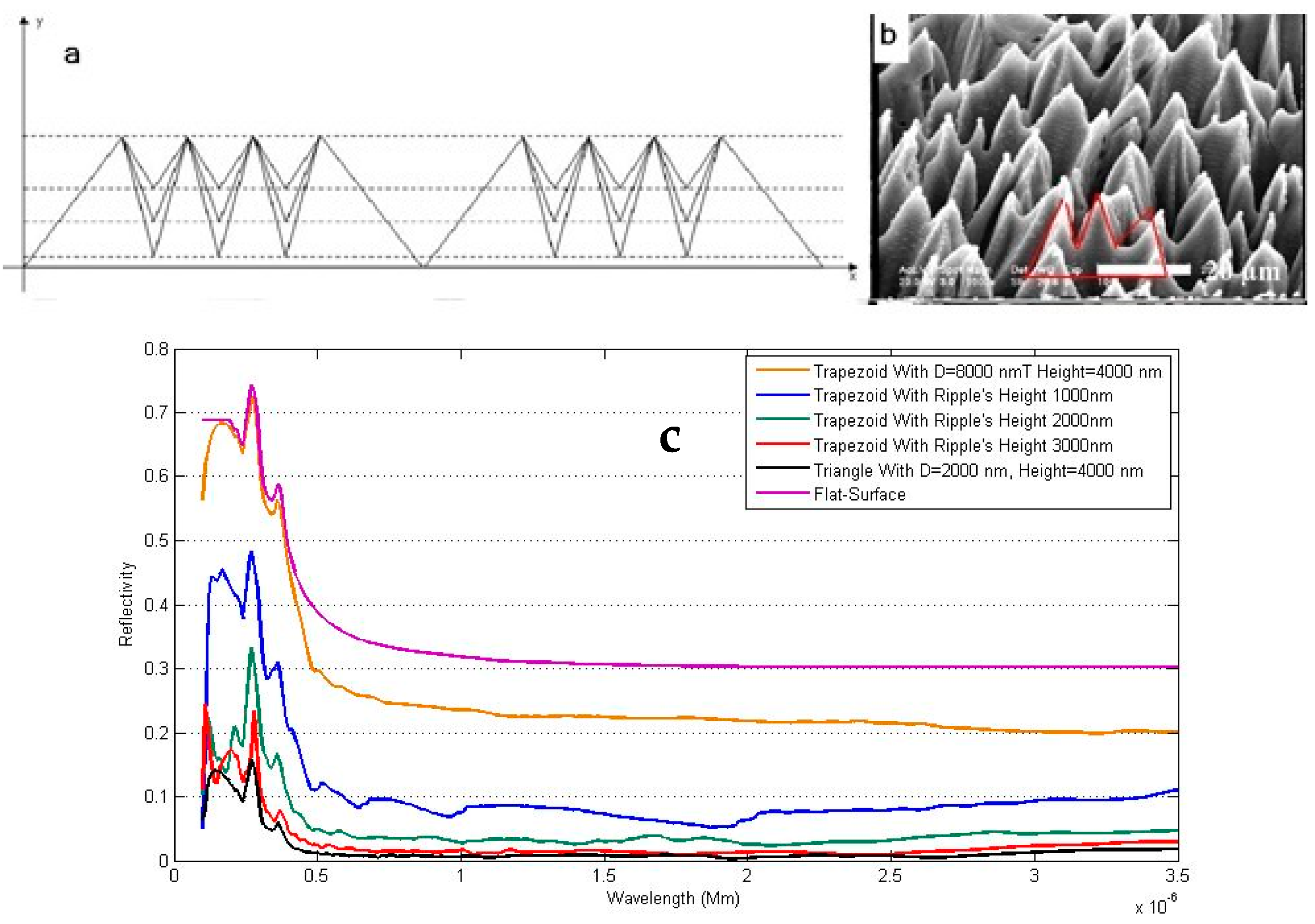
Figure 9a depicts the structural trapezoid scheme that appears in the SEM images, as shown in Figure 9b. In the following, these microstructures are examined. Figure 9c plots the spectral reflectance diagrams of the texturing surfaces similar to Figure 9a. The spectral reflection begins to flatten for wavelengths longer than ~500 nm. Contrary to the results of the structures in Figure 4, showing lower reflectance for wavelengths shorter than 500 nm for larger wavelengths. These microstructures benefit from higher reflectance for wavelengths shorter than 500 nm for larger wavelengths. This suggests these different structures are combined randomly. The final spectral reflectance would be smoother for a wide spectral range.

3.3. Hybrid Model

Finally, due to the existence of all the structures described above, in the structures formed by excimer laser radiation, the final spectral reflectance in favor of the microstructures of interest must be the resultant of all the profiles given above. Due to the effect of some texturing at shorter and longer wavelengths, the final profile will be much smoother for a wide range of wavelengths.
The spectral reflectance of needle-type microstructures characterizes a very small periodicity and a very large height. The results were significant for the wavelength range over 400–1100 nm. These textures exhibit a height ~30 times larger than the periodicity, as shown in Figure 10. Samples with a periodicity greater than 40 nm show a reflectance of less than 1%, which can be introduced as structures with very low reflection addressing many potential applications.
The microcones created by excimer laser radiation consist of a distributed combination of trapezoidal and triangular structures over rippling morphology. At first, their behavior at different wavelengths is assessed by modeling with triangular structures. However, the results obtained approximating these structures with triangular structures do not meet the experimental structure behavior. Upon further examination of the SEM images presented in [9], it was observed that in some cases, the juxtaposition of these microcones causes the formation of other microstructures, as shown in Figure 4 and Figure 9. After studying the behavior of these textures at different wavelengths, it is observed that each of them reduces the surface reflection at a certain range of wavelengths. Indeed, the spectral reflectance is significantly reduced and simultaneously flattened over the visible spectral range [19]. Subsequently, the trapping of light in the small pores notably increases the rate of electron-hole production so that the efficiency of the solar cell is elevated accordingly. Finally, the plausible conclusion is reached by juxtaposing these two different microstructures intermittently and sporadically, and the result obtained for the whole structure is very close to the experimental results in favor of the hybrid model.

4. Conclusions

This investigation improves our vision regarding the surface texturing of silicon in solar cell assembly for the purpose of efficiency enhancement. In general, the skin rippling results in the reflectance reduction against the non-rippling textures. The triangular morphology in the form of the equilateral altering triangles with different periodicities emphasizes the reduction of the surface reflectance over 400–1500 nm. Particularly, these structures notably reduce the surface spectral reflection ranging from 200 to 500 nm. Furthermore, the trapezoidal structures are examined with periodic surface ripples that attest to spectral smoothing alongside the surface reflectance reduction for wavelengths longer than 500 nm. The profiles of the spectral reflectance for both triangular and trapezoidal structures with different heights and fixed periodicity indicate that the larger height gives rise to the further reduction of the spectral reflectance. Note that the trapezoid scheme undergoes much smaller spectral reflectance longer than ~500 nm against those of the triangular model. On the other hand, ray optics emphasizes that the number of collisions of incident light with lateral walls of microstructures notably enhances mainly due to more efficient photon trapping events. The trapping of light in the small pores notably increases the rate of electron-hole generation so that the harvesting of solar cells is effectively elevated. Moreover, the enlargement of periodicity broadens the spectral range in which the reflectance profile becomes smoother. In fact, at shorter periodicity, the reflectance levels down in favor of shorter wavelengths, and it starts elevating for the longer wavelengths. This mainly arises from the fact when the wavelength of the incident light becomes closer, the texturing dimensions and the optimal condition takes place, leading to more efficiency of the treated solar panels. The hybrid triangular/trapezoidal architecture is shown to simulate the actual excimer laser-induced texturing on the silicon surface in agreement with the experimental results regarding spectral reflectance.

Author Contributions

Conceptualization, P.P. and H.R.D.; methodology, H.R.D.; software, A.C.; validation, H.R.D., P.P. and A.C.; formal analysis, H.R.D.; investigation, P.P., S.Z.M., A.R. and M.A.; resources, S.Z.M. and A.R.; data curation, S.Z.M., A.R. and M.A.; writing—original draft preparation, H.R.D.; writing—review and editing, P.P., H.R.D. and M.A.; visualization, H.R.D.; supervision, P.P. and H.R.D.; project administration, P.P., H.R.D. and M.A.; Funding acquisition, P.P., and M.A. All authors have read and agreed to the published version of the manuscript.

Funding

This research received no external funding.

Data Availability Statement

Not applicable.

Conflicts of Interest

The authors declare no conflict of interest.

References

  1. Kumar, V.; Verma, R.; Kango, S.; Sharma, V. Recent progresses and applications in Laser-based surface texturing. Systems. Mater. Today Commun. 2021, 26, 101736. [Google Scholar] [CrossRef]
  2. Wang, Z.; Song, J.; Wang, T.; Wang, H.; Wang, Q. Laser Texturing for Superwetting Titanium Alloy and Investigation of Its Erosion Resistance. Coatings 2021, 11, 1547. [Google Scholar] [CrossRef]
  3. Mao, B.; Siddaiah, A.; Liao, Y.; Menezes, P.L. Laser surface texturing and related techniques for enhancing tribological performance of engineering materials: A review. J. Manuf. Process. 2020, 53, 153–173. [Google Scholar] [CrossRef]
  4. Yaddadenea, C.; Djemaaa, A.; Belaroussib, Y.; Kerdjab, T.; Gabouzea, N.; Keffousa, A.; Guerbousc, L. Optical properties of silicon microcolumn grown by nanosecond pulsed laser irradiation. Opt. Commun. 2011, 284, 3308–3310. [Google Scholar] [CrossRef]
  5. Wu, C.; Crouch, C.H.; Zhao, L.; Carey, J.; Younkin, E.R.; Levinson, J.A.; Mazur, E.; Farrell, R.M.; Gothoskar, P.; Karger, A. Near-unity below-band-gap absorption by microstructured silicon. Appl. Phys. Lett. 2001, 78, 1850. [Google Scholar] [CrossRef]
  6. Lowndes, D.H.; Fowlkes, J.D.; Pedraza, A.J. Early stages of pulsed-laser growth of silicon microcolumns and microcones in air and SF6. Appl. Surf. Sci. 2000, 154–155, 647–658. [Google Scholar] [CrossRef] [Green Version]
  7. Available online: http://www.mazur.harvard.edu/ (accessed on 2 September 2004).
  8. Her, T.H.; Finlay, R.J.; Wu, C.; Mazur, E. Femtosecond laser-induced formation of spikes on silicon. Appl. Phys. A 2000, 70, 383. [Google Scholar] [CrossRef]
  9. Bassam, M.A.; Parvin, P.; Sajad, B.; Moghimi, A.; Coster, H. Measurement of optical and electrical properties of silicon microstructuring induced by ArF excimer laser at SF6 atmosphere. Appl. Surf. Sci. 2008, 254, 2621–2628. [Google Scholar] [CrossRef]
  10. Dehghanpour, H.R.; Parvin, P.; Sajad, B.; Nour-Azar, S.S. Dose and pressure dependence of silicon microstructure in SF6 gas due to excimer laser irradiation. Appl. Surf. Sci. 2009, 255, 4664–4669. [Google Scholar] [CrossRef]
  11. Dehghanpour, H.R.; Parvin, P. Fluorine penetration into amorphous SiO2 glass at SF6 atmosphere using Q-switched Nd: YAG and excimer laser irradiations. Jpn. J. Appl. Phys. 2010, 49, 075803. [Google Scholar] [CrossRef]
  12. Dehghanpour, H.R.; Parvin, P. Glass surface modification using Nd: YAG laser in SF6 atmospheres. J. Theor. Appl. Phys. 2015, 9, 135–140. [Google Scholar] [CrossRef] [Green Version]
  13. Dehghanpour, H.R.; Parvin, P.; Abdolahi, S. Performance enhancement of solar panel by surface texturing using ArF excimer laser. Optik 2015, 126, 5496–5498. [Google Scholar] [CrossRef]
  14. Llopis, F.; Tobías, I. Influence of texture feature size on the optical performance of silicon solar cells. Prog. Photovol. 2005, 15, 27–36. [Google Scholar] [CrossRef]
  15. Refahizadeh, M.; Parvin, P.; Silakhori, K.; Mortazavi, S.Z.; Reyhani, A.; Abolhosseini, S.; Hojati Rad, H.; Majdabadi, A. Formation of ArF laser-induced self-assembled macrostructures on poly methyl methacrylate and CR-39 polymers. J. Laser Appl. 2017, 29, 022008. [Google Scholar] [CrossRef]
  16. Refahizadeh, M.; Parvin, P.; Silakhori, K.; Mortazavi, S.Z.; Mehdilo, A. Fabrication of self-ruled micro grating on CR-39 using ArF laser-induced rippling. Laser Phys. 2017, 27, 066101. [Google Scholar] [CrossRef]
  17. Refahizadeh, M.; Majdabadi, A.; Parvin, P.; Silakhori, K.; Mortazavi, S.Z.; Mehdilo, A.; Aghaii, P. Angular dependence of ArF laser induced self-aligning microstructures on CR39. Opt. Mater. Exp. 2015, 5, 1543–1549. [Google Scholar] [CrossRef]
  18. Parvin, P.; Refahizadeh, M.; Mortazavi, S.Z.; Silakhori, K.; Mahdiloo, A.; Aghaii, P. Regular self-microstructuring on CR39 using high UV laser dose. Appl. Surf. Sci. 2014, 292, 247–255. [Google Scholar] [CrossRef]
  19. Parvin, P.; Reyhani, A.; Mehrabi, M.; Refahizadeh, M.; Mortazavi, S.Z.; Ranjbar, A. Efficiency enhancement using ArF laser induced micro/nanostructures on the polymeric layer of solar cell. Opt. Laser Tech. 2017, 88, 242–249. [Google Scholar] [CrossRef]
  20. Gholizadeh, A.; Reyhani, A.; Parvin, P.; Mortazavi, S.Z.; Mehrabi, M. Enhancement of Si solar cell efficiency using ZnO nanowires with various diameters. Mater. Res. Exp. 2018, 5, 015040. [Google Scholar] [CrossRef]
  21. Gholizadeh, A.; Reyhani, A.; Parvin, P.; Mortazavi, S.Z. Efficiency enhancement of ZnO nanostructure assisted Si solar cell based on fill factor enlargement and UV-blue spectral down-shifting. J. Phys. D Appl. Phys. 2017, 50, 185501. [Google Scholar] [CrossRef]
  22. Smith, M.S.D. Application of the Differential Method to Diffraction Gratings That Utilize Total Internal Reflection Facets. Ph.D. Thesis, University of Manitoba, Winnipeg, MB, Canada, 1998. [Google Scholar]
  23. Bai, B.; Li, L. Improving the Fourier modal method for crossed gratings with C3 symmetry by using a group-theoretic approach. Proc. SPIE 2005, 5636, 1–11. [Google Scholar]
  24. Vincent, P. A finite-difference method for dielectric and conducting crossed gratings. Opt. Commun. 1978, 26, 293–296. [Google Scholar] [CrossRef]
  25. Maystre, D.; Nevière, M. Electromagnetic theory of crossed gratings. J. Opt. 1978, 9, 301–306. [Google Scholar] [CrossRef]
  26. Han, S.T.; Tsao, Y.L.; Walser, R.M.; Becker, M.F. Electromagnetic scattering of two-dimensional surfacerelief dielectric gratings. Appl. Opt. 1992, 31, 2343–2352. [Google Scholar] [CrossRef]
  27. Dobson, D.C.; Cox, J.A. An integral equation method for biperiodic diffraction structures. In International Conference on the Application and Theory of Periodic Structures; Lerner, J.M., McKinney, M.R., Eds.; 1991; Volume 1545, pp. 106–113. Available online: https://www.spiedigitallibrary.org/conference-proceedings-of-SPIE/1545.toc (accessed on 10 September 2022).
  28. Derrick, G.H.; McPhedran, R.C.; Maystre, D.; Nevière, M. Crossed gratings: A theory and its applications. Appl. Phys. 1979, 18, 39–52. [Google Scholar] [CrossRef]
  29. McPhedran, R.C.; Derrick, G.H.; Nevière, M.; Maystre, D. Metallic crossed gratings. J. Opt. 1982, 13, 209–218. [Google Scholar] [CrossRef]
  30. Harris, J.B.; Preist, T.W.; Sambles, J.R.; Thorpe, R.N.; Watts, R.A. Optical response of bigratings. J. Opt. Soc. Am. A 1996, 13, 2041–2049. [Google Scholar] [CrossRef]
  31. Granet, G. Analysis of diffraction by surface-relief crossed gratings with use of the Chandezon method: Application to multilayer crossed gratings. J. Opt. Soc. Am. A 1998, 15, 1121–1131. [Google Scholar]
  32. Bräuer, R.; Bryngdahl, O. Electromagnetic diffraction analysis of two-dimensional gratings. Opt. Commun. 1993, 100, 1–5. [Google Scholar] [CrossRef]
  33. Noponen, E.; Turunen, J. Eigenmode method for electromagnetic synthesis of diffractive elements with threedimensional profiles. J. Opt. Soc. Am. A 1994, 11, 2494–2502. [Google Scholar]
  34. Li, L. New formulation of the Fourier modal method for crossed surface-relief gratings. J. Opt. Soc. Am. A 1997, 14, 2758–2767. [Google Scholar] [CrossRef]
  35. Greffet, J.J.; Baylard, C.; Versaevel, P. Diffraction of electromagnetic waves by crossed gratings: A series solution. Opt. Lett. 1992, 17, 1740–1742. [Google Scholar] [CrossRef] [PubMed]
  36. Bagnoud, V.; Mainguy, S. Diffraction of electromagnetic waves by dielectric crossed gratings: A three-dimensional Rayleigh-Fourier solution. J. Opt. Soc. Am. A 1999, 16, 1277–1285. [Google Scholar] [CrossRef]
  37. Bruno, O.P.; Reitich, F. Numerical solution of diffraction problems: A method of variation of boundaries. III. Doubly periodic gratings. J. Opt. Soc. Am. A 1993, 10, 2551–2562. [Google Scholar] [CrossRef]
  38. Bruno, O.P.; Reitich, F. Calculation of electromagnetic scattering via boundary variations and analytic continuation. Appl. Computat. Electromagn. Soc. J. 1996, 11, 17–31. [Google Scholar]
  39. Li, L.; Chandezon, J.; Granet, G.; Plumey, J.P. Rigorous and efficient grating-analysis method made easy for optical engineers. Appl. Opt. 1999, 38, 304–313. [Google Scholar] [CrossRef]
  40. Chandezon, J.; Maystre, D.; Raoult, G. A new theoretical method for diffraction gratings and its numerical application. J. Opt. 1980, 11, 235–241. [Google Scholar] [CrossRef] [Green Version]
  41. Chandezon, J.; Dupuis, M.T.; Cornet, G.; Maystre, D. Multicoated gratings: A differential formalism applicable in the entire optical region. J. Opt. Soc. Am. 1982, 72, 839–846. [Google Scholar] [CrossRef]
  42. Liu, H. Coordinate transformation method for modeling three-dimensional photonic structures with curved boundaries. Opt. Exp. 2021, 29, 1516–1531. [Google Scholar] [CrossRef]
  43. Ming, X.; Sun, L. Simple reformulation of the coordinate transformation method for gratings with a vertical facet or overhanging profile. Appl. Opt. 2021, 60, 4305–4314. [Google Scholar] [CrossRef]
  44. Yue, L.; Cheng, D.; Qiao, Y.; Zhao, J. Error Calibration for Full Tensor Magnetic Gradiometer Probe Based on Coordinate Transformation Method. IEEE Trans. Instrum. Meas. 2022, 71, 1–11. [Google Scholar] [CrossRef]
  45. Petit, R. (Ed.) Electromagnetic Theory of Gratings; Springer-Verlag: Berlin-Heidelberg, Germany; New York, NY, USA, 1980. [Google Scholar]
  46. Popov, E. Gratings: Theory and Numeric Application; Institut Fresnel: Marseille, France, 2014. [Google Scholar]
Figure 1. (a) Notation and Cartesian coordinate system for a typical grating, triangular morphology (blue) and trapezoidal scheme (red). (b) Definition of the spatial domains D+, D, D1 and D2.
Energies 15 07540 g001
Figure 2. Spectral reflectance of a triangular simulation with (a) several different periodicities and (b) three different periodicities taken from reference [18], (c) and (d) the outputs of our code for the examples given in (a) and (b), respectively.
Energies 15 07540 g002
Figure 3. (a) Selective periodic texturing with three aspect ratios (64/14, 70/14 and 100/14) for simulation, (b) surface spectral reflectance for three triangular microstructures of interest with a base of 14 nm and the aspect ratio of 64/14, 70/14 and 100/14. Note that the green curve addresses a reflectance of less than 10%.
Energies 15 07540 g003
Figure 4. (a) Experimental triangular microstructures on Si surface [9], (b) Schemes of the microstructure of interest for simulation with programming code, (c) Simulation result for microstructures with a periodicity of 11, 21, 25 and 30 μm. The height of the structures for a typical sample with a periodicity of 30 μm is set to be ~13 μm.
Energies 15 07540 g004aEnergies 15 07540 g004b
Figure 5. (a) Spectral reflection using simulation of the texturing with different coefficients of y1 and y2 equations and periodicities of 11, 21, 25 having 30 μm. The height of the structure for the period of 30 μm is set to be 15 μm, (b) comparison of two microstructures with periods of 25 and 30 μm. Note that the larger the number of ripples, the lower the skin’s spectral reflectance.
Energies 15 07540 g005
Figure 6. Spectral reflection of triangular surface rippling of triangular microstructures.
Energies 15 07540 g006
Figure 7. (a) Schemes of height distribution of triangular microstructure, (b) Spectral reflection based on the base size and height of triangular microstructures.
Energies 15 07540 g007
Figure 8. Simulation results for spectral reflection of surfaces with different microstructures by changing the leg angle. D stands for degree.
Energies 15 07540 g008
Figure 9. (a) Trapezoid-like structures selected for simulation. (b) Real trapezoidal structures observed in SEM image of the surface texturing [9], (c) Simulation results for the microstructures with periodicity and height of 8 and 4 μm, respectively. Note that the trapezoidal scheme undergoes smaller spectral reflectance for wavelengths longer than ~500 nm with respect to those of the triangular model.
Energies 15 07540 g009
Figure 10. Spectral reflectance of the needle-like microstructures according to the height and periodicity mentioned in the legend.
Energies 15 07540 g010
Publisher’s Note: MDPI stays neutral with regard to jurisdictional claims in published maps and institutional affiliations.