Abstract
This paper presents a triple-mode average current control (TACC) strategy to achieve unity power factor and reduce the current stress for a boost PFC converter. The controller switches among different modes in each half-line cycle, and smooth transition is ensured by mapping of the operation region. By adaptive mode shifting, it reduces the current stress and current distortion caused by non-linear effects. With valley current shaping and comparisons, the TACC controller accordingly incorporates three control laws to adapt different modes. In discontinuous conduction mode (DCM), a variable on-time is calculated while the modulation is equivalent to PWM. In critical conduction mode (CRM), a constant on-time is derived, while the switching cycle is modified to regulate the current average value. For both DCM and CRM, the switching cycle is slightly extended to realize valley switching. Furthermore, with valley current shaping, the proposed controller reuses the CRM calculation to form continuous conduction mode (CCM) control law. To make the control laws compatible, normalized mapping and design rules are provided with respect to mode boundaries. This allows the TACC controller to automatically switch among different modes. Finally, experimental results prove the effectiveness of the controller in reducing the current stress and enlarging the preferable power range.
Keywords:
boost; CCM; CRM; current mode control; current stress; DCM; harmonic distortion; power factor 1. Introduction
Boost PFC converters are widely used in industrial applications, such as LED drivers [1,2], uninterruptible power supplies (UPS) [3,4] and on-board chargers [5,6], etc. In order to meet industrial standards (such as IEC 61000-3-2 and IEEE Std 519), some consistent pursuits are to improve the power factor, improve the efficiency and reduce the current harmonics. With respect to continuity of inductor current, the converter can operate in discontinuous conduction mode (DCM), critical conduction mode (CRM) or continuous conduction mode (CCM). Since the operation modes suit different power levels, a great challenge is to carry out the optimizations over a wide operation range.
When a boost PFC converter operates in DCM, it has the advantages of constant switching frequency, reduced reverse recovery of diode, and zero inductor current lag [7,8]. Variable on-time (VoT) controls are proposed to regulate the input current as sinusoid, which greatly improves the power factor under DCM [9]. Furthermore, by discretely fitting VoT, digital pulse train controls can simplify the realization and reduce the hardware cost [10]. However, DCM operation can induce high current stress and conduction loss. This issue can be alleviated by artificially introducing harmonics into the input current, which slightly compromises the power factor [8,11]. For CRM operation, it is conventionally controlled with constant on-time (CoT) [12,13]. The advantage lies in its potential to achieve valley switching, which improves the light load efficiency. However, considerable zero-crossing distortion can be induced by negative current and other nonlinear effects when the on-time is short. To offset the negative current effect caused by parasitic oscillation, variable on-time controls are proposed to lengthen the on-time when the line voltage is low [14,15,16,17,18]. CCM operation is preferable in reducing the current stress and conduction loss. However, the inductor current lag complicates the controller design and power factor correction. This issue can be addressed by current mode controls with accurate reference current tracking, such as predictive digital current mode control [19,20], pulse train current mode control [21], etc. Average current mode control (ACMC) and one-cycle control (OCC) operating in CCM can achieve great performance with certain loads [22]. However, as the converter is forced into DCM under light load and near zero-crossing, an erroneous CCM control law can lead to considerable zero-crossing distortion. To ensure consistent CCM operation, the switching frequency should increase dramatically near zero-crossing and under light load, which leads to high switching loss [23,24].
Furthermore, control strategies are proposed to achieve mixed DCM/CCM operation to combine their advantages. However, the operation modes have different dynamic models that induce contradictory control laws. In [25,26], an adaptive digital controller achieves both DCM and CCM in each half-line cycle. Based on zero current events, a digital DCM detection method is used to select linear compensators for the loop. In [27], digital peak current mode control for mixed DCM/CCM operation is proposed. It adopts a finite-state machine and a look-up-table for selecting the operation mode and switching frequency. To reduce toggling during mode transition, valley estimation and ripple comparison methods are used for mode detection [28]. In simplifying digital realization, [29] presents an average current mode control for a bridgeless boost PFC converter to achieve mixed DCM/CCM operation. It adopts a Taylor series fitted-duty ratio, which effectively reduces digital calculations.
Other studies focus on control strategies to achieve mixed DCM/CRM operation. These two operations also induce different dynamic models and contradictory control laws. To address this issue, load-dependent operation-mode selection strategy is proposed to achieve either DCM or CRM in a half-line cycle [30]. With an analog circuit, [31] proposes a controller to achieve constant on-time under CRM and constant duty ratio under DCM. When mixing DCM and CRM in a single half-line cycle, an important issue lies in the current distortion caused by switching node resonance, which should be compensated to improve the THD [32].
Owing to the contradictory control laws, the existing mixed-mode controls focus on either mixed DCM/CCM or mixed DCM/CRM operations. Comparatively, mixed DCM/CCM operation usually loses valley switching, which harms the light load efficiency. Mixed DCM/CRM operation suffers high current stress at high power, which limits the power range.
Aiming at improving comprehensive performance over a wide operating range, the TACC control is proposed in this paper. The controller can switch among DCM/CRM/CCM operations in each half-line cycle, and smooth transition is ensured by mapping of the operation region and power level. When the instant power is low, the controller achieves DCM operation, which limits the switching frequency and reduces negative current effect. The switching cycle is constant while the on-time is modulated to regulate the input current. As the instant power increases, the controller automatically switches to CRM operation to improve efficiency, which adopts a constant on-time to regulate the input current as the shape of input voltage. For both DCM and CRM, the switching cycle is slightly extended to realize either valley switching or zero voltage switching. When the instant power is high enough, the controller levels up the valley current to achieve CCM operation, which is realized by a valley current shaping module. The partial CCM operation reduces the current ripple and stress at high voltage and heavy load. Both on-time and switching cycle are modulated to regulate the input current as sinusoid. Furthermore, normalized analyses and simulations are provided to evaluate the power range and current stress. With integrated control laws and valley current shaping, the TACC controller enlarges the preferable voltage and power range and improves the comprehensive performance over a wide operating range, effects that are verified by the experimental results.
This paper is organized as follows. Section 2 provides conventional control strategies for boost PFC converter operating in single DCM and CRM. In Section 3, the proposed TACC control strategy is introduced, including the control algorithm, design rules, operation region analyses and performance evaluations. Simulations and experimental results are provided in Section 4 and Section 5, respectively. Finally, a brief conclusion is given in Section 6.
2. Conventional Control Strategies for a Boost PFC Converter Operating in Single DCM or CRM
A scheme of a basic boost PFC converter is given in Figure 1. The front-end input filter is used to reduce the EMI and voltage ripple. With full bridge and Cg, the line voltage is regulated as a smooth line voltage of vg = |vin|. Furthermore, the boost stage regulates the voltage as vout. Unity power factor is achieved when iin is regulated as the shape of vin. When the phase shift of the input filter is small, this can be achieved by regulating iL,av (denoting average value of iL) as the shape of vg. Therefore, the boost stage should be controlled as a resistive load while boosting vg to vout. Depending on the continuity of the inductor current, the boost stage can operate in DCM, CRM or CCM.
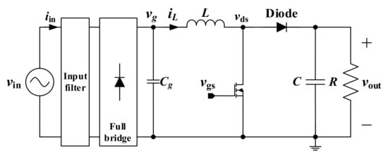
Figure 1.
Boost PFC converter scheme.
With the use of conventional PWM to achieve DCM, a variable on-time can regulate iL,av as the shape of vg. However, the instant power is always limited by the DCM boundary. Detailed control strategy and the maximum instant power are analyzed in Section 2.1. When operating in single CRM, iL,av is proportional to the product of on-time and vg. Therefore, constant on-time can regulate iL,av as the shape of vg. However, depending on power and voltage levels, CRM operation leads to a high dynamic switching frequency. This challenges the input filter design, ripple reduction and speed of power switches, which will be analyzed in Section 2.2.
2.1. Variable On-Time Control to Achieve DCM Operation
To improve the power factor under DCM, variable on-time is required to achieve sinusoid iL,av, as shown in Figure 2.
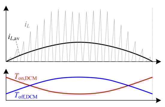
Figure 2.
Variable on-time for PWM to achieve sinusoid iL,av.
The boost stage should regulate iL,av as the shape of vg. When operating in DCM, iL,av is given by:
where Ton,DCM denotes the on-time to achieve DCM. Assuming iL,av = Irefvg/Vg (Vg is magnitude of vg, while Iref is magnitude reference for iL,av), the required Ton,DCM is:
This variable on-time can achieve near unity power factor under PWM, whereas the instant power is limited by DCM boundary. With the boundary condition Ton,DCM < (vout − vg) T/vout, the instant input power (denoted as Pin,inst) is limited by:
Although increasing T/L can alleviate this issue, a high T/L can increase the current ripple and stress on power devices.
2.2. Constant On-Time Control to Achieve CRM Operation
Comparatively, CRM does not suffer the boundary issue, while it reduces the current stress. To regulate the input current, a constant on-time is usually adopted, as shown in Figure 3.
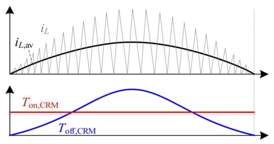
Figure 3.
Constant on-time to achieve CRM operation and sinusoid iL,av.
When a boost PFC converter operates in CRM, iL,av is half of the inductor current peak value:
where Ton,CRM denotes the on-time to achieve CRM. Based on (4), a constant Ton,CRM will regulate iL,av as the shape of vg. However, with different input and power levels, the required Ton,CRM could change dramatically. Assuming magnitude of iL,av is regulated as Iref, the required Ton,CRM is:
Furthermore, based on voltage-second balancing, Toff,CRM is given by:
With Ton,CRM and Toff,CRM, the achieved switching cycle is given by:
With varying vg and Pin,inst, the achieved switching cycle could change dramatically.
2.3. Current Stress and the Current Distortion Caused by Negative Current and Non-Linear Effects
The strategies mentioned above have issues in current stress and current distortion, since they are in single DCM or single CRM operations. Considering switching transients and current stress, the inductor currents under different modes are given by Figure 4.
Figure 4.
Inductor currents under different operation modes considering switching transients and current stresses.
For DCM and CRM operations, the inductor current peak values are given by (8).
Since T > Ton,DCM+Toff,DCM, the current stresses are always higher than 2iL,av, which is not beneficial to power devices. Furthermore, non-linear effects can induce considerable distortion to iL,av. This is especially true for CRM near the zero-crossing point, where the negative current effect is evident. This is because CRM has lower positive current part in each switching cycle. Compared with DCM and CRM operations, CCM operation can effectively reduce the current stress under the same iL,av. Moreover, it eliminates the negative current effect. However, when iL,av is very low, the required switching frequency is too high to be operational. For CRM and CCM operations, either the negative current effect or the high switching frequency can induce considerable zero-crossing distortion, since iL,av is very low near the zero-crossing point.
In conclusion, CCM operation is preferable to reduce the current stress, since it reduces the inductor current peak value below 2iL,av. Thus, it can improve the power level under the same current stress. To avoid current distortion near the zero-crossing point, DCM operation is preferable, since the current average value is less affected by the negative current effect. To address the above-mentioned issues simultaneously, the TACC control strategy is proposed in the followings.
3. Triple-Mode Average Current Control to Achieve Mixed DCM/CRM/CCM Operation
Overall scheme of TACC control strategy is given by Figure 5, while the typical waveforms are in Figure 6. Compared with control strategies in Section 2, TACC incorporates three control laws to adapt different operation modes. Moreover, it incorporates feedforward actions to perform valley current shaping and on-time calculations. The line voltage (vg) is sampled for calculations of iv,ref, Ton,CRM&CCM and Ton,DCM. With valley current shaping and simple comparisons, the converter can automatically switch among DCM/CRM/CCM operations.
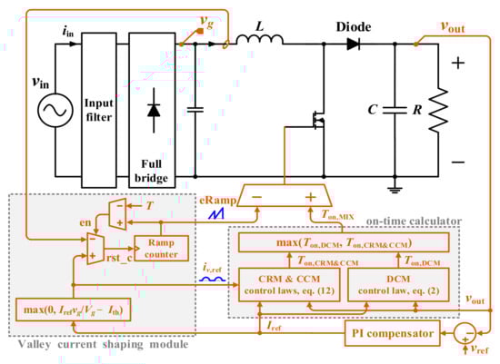
Figure 5.
Boost PFC converter and the TACC control scheme to achieve mixed DCM/CRM/CCM operation.
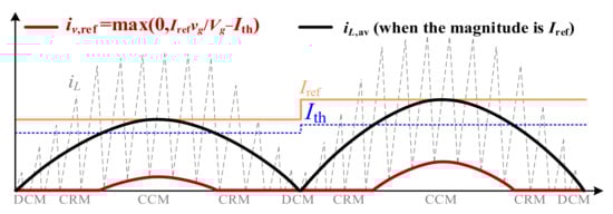
Figure 6.
Mixed DCM/CRM/CCM operation with TACC control.
The proposed TACC controller includes an on-time calculator that incorporates DCM/CRM/CCM control laws, a PI compensator to generate the reference current (Iref), and a valley current shaping (VCS) module to regulate the inductor current valley value under CCM. The VCS module generates two outputs: a reference to regulate the inductor current valley value (iv,ref) and an extended ramp signal (eRAMP). When eRAMP is higher than T while the inductor current is lower than iv,ref, a new switching cycle is initiated by resetting eRAMP. Magnitude of iv,ref is adjusted by (9), so as to suit different operation modes.
where Ith is a threshold to trigger CCM operation (updated every half-line cycle). When Irefvg/Vg ≤ Ith, the calculated iv,ref is clamped as zero, and the converter achieves DCM or CRM operations. When Irefvg/Vg > Ith, the calculated iv,ref is positive, and the converter achieves CCM operation.
For DCM operation, iL ≤ iv,ref is immediately detected once eRAMP is higher than T; thus, the achieved switching cycle is T. For CRM and CCM operations, the VCS module dynamically alters the turn-on point of each switching cycle, resulting in a higher switching cycle. In this way, the TACC controller incorporates three control laws to suit DCM/CRM/CCM operations. A small delay (td) is artificially added in transmitting rst_c, so as to achieve either valley switching or zero voltage switching under DCM and CRM. This helps to improve the overall efficiency, especially at light load. To achieve valley switching, td should be set as 1/4 of the parasitic resonant cycle, i.e., , where Coss is the output capacitance of power switch and Cj is the junction capacitance of the diode.
Algorithms and design rules of the TACC controller are given in Section 3.1. Normalized conditions and operation regions under TACC control are analyzed in Section 3.2, while a comprehensive evaluation for the proposed control is given in Section 3.3.
3.1. Algorithms and Design Rules of TACC Control
For all operation modes, the magnitude of iL,av should be regulated as Iref, i.e., the output of the PI compensator. To regulate iL,av, a variable on-time calculator is used to calculate Ton,MIX of each switching cycle:
where Ton,DCM is the same as (2), and Ton,CRM&CCM is the on-time for CRM and CCM operations. Assuming that valley value of iL is regulated as iv,ref, then iv,av is given by (11) under CRM and CCM operations.
Furthermore, substituting iL,av = Irefvg/Vg into (11) gives the required Ton,CRM&CCM to achieve the unity power factor:
With (10), the finally calculated on-time is the higher value of Ton,DCM and Ton,CRM&CCM. However, the relationship between Ton,DCM and Ton,CRM&CCM could change dynamically in a half-line cycle. Potential operation modes within a half-line cycle are given in Figure 7a. iv,ref is consistent zero, which disables CCM operation. Depending on the relationship between Ton,DCM and Ton,CRM&CCM, the converter achieves mixed DCM/CRM, single DCM or single CRM operations. In Figure 7b, iv,ref becomes positive at the middle of the half-line cycle, which enables CCM operation. The converter achieves CCM operation only when Ton,DCM < Ton,CRM&CCM and iv,ref > 0.
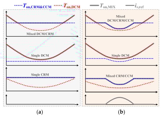
Figure 7.
Potential operation modes with different iv,ref, Ton,DCM and Ton,CRM&CCM. (a) Operations with iv,ref = 0; (b) operations with dynamic changing iv,ref.
When Ton,DCM > Ton,CRM&CCM and iv,ref > 0, erroneous operation occurs, which must be prevented by an appropriate Ith. In this situation, a positive iv,ref intends to achieve CCM operation, whereas the on-time calculator sets Ton,MIX = Ton,DCM. The error will deviate the inductor current under CCM, since the required on-time is smaller than the calculated result. To prevent this, a suitable Ith should guarantee Ton,CRM&CCM ≥ Ton,DCM when iv,ref is positive, i.e.:
Substituting into (13) derives:
According to (14), erroneous operations can be effectively prevented by selecting a high Ith. However, as a threshold to trigger CCM operation, Ith determines the portion of CCM operation and magnitude of iv,ref. When Ith is too high, inadequate CCM operation cannot effectively suppress the current ripple and current stress. Therefore, an appropriate strategy is to set Ith exactly as:
Modulating Ith directly with (15) requires extensive calculations, since vg changes every switching cycle. Nevertheless, (15) reaches its maximum value when vg = 2vout/3. Therefore, substituting vg = 2vout/3 into (15) gives a sufficient condition to prevent erroneous operations:
Compared with (15), this result is simplified to a considerable extent. Moreover, both Iref and Vg change every half-line cycle, while variation of vout within a half-line cycle is usually small. Therefore, the calculation only needs to be updated every half-line cycle.
3.2. Operation Regions under TACC Control
With TACC control, the converter will automatically switch among DCM/CRM/CCM operations while regulating the input current as sinusoid. The achieved operation mode depends on Iref, vout, vg and Vg. Since the on-time and iv,ref are calculated by (10) and (9), the conditions to achieve DCM/CRM/CCM operations are summarized as:
Furthermore, to facilitate universal analysis, normalizing the conditions with F1 and F2:
where F1 is the normalized line voltage and F2 is the normalized ratio between Iref and Vg. Substituting (2), (12), (16) and (18) into (17) gives:
For any positive variable x, maximum value of x2(1 − x) is exactly 4/27 (when x = 2/3). Therefore, is consistently valid, while
is necessarily valid when . Furthermore, (19) is simplified as:
Based on (20), mapping of operation regions under TACC control is plotted in Figure 8.
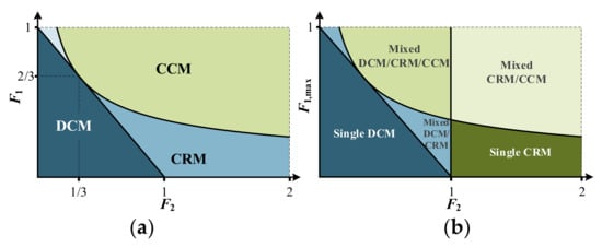
Figure 8.
Mapping of operation regions under TACC control. (a) Instant operation modes with F1 and F2; (b) mode mixing in a half-line cycle with F1,max and F2.
The instant operation mode is directly determined by F1 and F2, as shown in Figure 8a. For F2 = 2LIref/(VgT), it is a constant value in each half-line cycle (both Iref and Vg are updated every half-line cycle). Therefore, smooth transition among different modes is ensured, as long as F1 = vg/vout changes smoothly without local oscillations. This can be easily guaranteed by the input filter and Cg.
In each half-line cycle, F2 is constant, while F1 changes between zero and F1,max (i.e., Vg/vout). Therefore, mode mixing in a half-line cycle is determined by F1,max and F2, as shown in Figure 8b. When F2 < 1, it achieves single DCM, mixed DCM/CRM or mixed DCM/CRM/CCM operations in a half-line cycle. When F2 > 1, it achieves single CRM or mixed CRM/CCM operations.
3.3. Comprehensive Evaluations for the Proposed TACC Control Strategy
Comprehensive evaluations for the proposed TACC control are given in aspects of the input power, on/off times, switching cycle and current stress. The TACC controller regulates magnitude of iL,av as Iref. Therefore, with F1 and F2 defined by (18), the instantaneous input power of boost stage is given by:
With unity power factor, the average input power is:
The final on-time Ton,MIX is determined by (2), (10) and (12), and the normalized value is given by:
The achieved switching cycle is either T or determined by the VCS module. Under DCM operation, the achieved switching cycle is nearly T, since rst_c (in Figure 5) becomes valid as soon as eRAMP reaches T. Under CRM and CCM operations, the achieved switching cycle is determined by iv,ref and voltage-second balancing of inductor. As a result, the final switching cycle under TACC control is given by:
In the aspect of current stress, based on Ton,MIX and iv,ref, the achieved inductor current peak value is given by:
As a conclusion to Section 3, this part proposes a TACC control strategy that achieves mixed DCM/CRM/CCM operation. Detailed analyses are provided with respect to the control scheme, design rules, operation regions and performance evaluations. The mode mixing can extend the power range through reducing the current stress, variation of on/off times and switching cycle. These are verified by simulations and experiments in the following section.
4. Simulations
Simulations were carried out in Matlab to verify the effectiveness of the proposed TACC control strategy. the detailed simulations included the achieved current stress and practical operation region with different controls. The main specifications of the power stage were the same as those in Table 1 (in Section 5).
4.1. Current Stress with Different Controls
Compared with conventional CoT control in the achievement of CRM, the proposed TACC controller reduces the inductor current peak value through CCM operation. With different controls, the normalized iL,pk values are plotted in Figure 9.
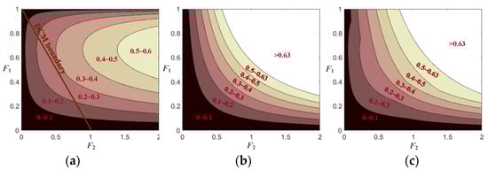
Figure 9.
Normalized inductor current peak value (i.e., iL,pk/(voutT/L)) with different controls. (a) VoT control to achieve DCM; (b) CoT control to achieve CRM; (c) TACC control to achieve mixed DCM/CRM/CCM.
For VoT control in the achievement of DCM, the normalized iL,pk is given by Figure 9a. Although the normalized current stress was low, the DCM boundary (F1 < 1-F2) strongly limited the power range. Reducing L could increase the power range, but this also increased the de-normalized iL,pk. For CoT control in achieving CRM, the normalized iL,pk was F1F2, which is plotted in Figure 9b. With the specifications presented in Table 1 (i.e., vout = 400 V, T = 10 μs, L = 350 μH), the de-normalized iL,pk was 7.2A when F1F2 = 0.63. Furthermore, considering current stress on power switches, the operation region was limited by F1F2 ≤ 0.63. For TACC control in the achievement of mixed-mode operation, the inductor current is given by (25). When , it achieved CCM operation, which reduced the inductor current peak value. Therefore, the non-operational region (F1F2 > 0.63, i.e., iL,pk > 7.2A) was smaller than that under CoT control.
4.2. Input Powers and Practical Operational Regions with Consideration of Current Stress and Minimum On-/Off-Times
The proposed TACC controller has a small current stress and reduced variation of on/off times. Therefore, compared with conventional CoT and VoT controls, it achieved a larger operational region. Practical operation regions with different controls are plotted in Figure 10. Considering power devices and non-linear effects, both the minimum on-/off-times were set as 0.05 (de-normalized as 0.05T = 0.5 μs) in the simulations. The maximum iL,pk was set as 0.63 (normalized to voutT/L) to reduce the current stress, which can be denormalized as iL,pk = 0.63voutT/L = 7.2 A.
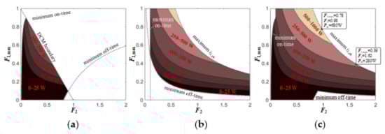
Figure 10.
Input power with consideration of minimum on/off times and current stress. (a) VoT control to achieve DCM; (b) CoT control to achieve CRM; (c) TACC control to achieve mixed DCM/CRM/CCM.
For VoT control to achieve DCM, the operational region is mainly limited by the DCM boundary and the minimum on-time. For CoT control to achieve CRM, the operation region is limited by the minimum on-/off-times and the maximum iL,pk. Moreover, the low power region is not operational owing to the minimum off-time. This leads to considerable zero-crossing distortion, since F1 necessarily changes from zero to F1,max in each half-line cycle. For the TACC controller to achieve mixed-mode operation, the operation region covers approximately ¾3/4 of the simulated area. Owing to the mixed-mode operation, the practical operation region is larger than the collection of the previous two controllers.
5. Experiments
An experimental prototype was built to verify effectiveness of the proposed TACC control strategy, as shown in Figure 11. To meet practical application requirements, the prototype was designed to adapt grid power supply instead of ideal AC source. The grid voltage has considerable noise, and can be affected by other grid connected devices. In this sense, an input filter is necessary to suppress exogenous noise and meet EMI requirements, which is specified in Appendix B. Furthermore, the control loop of the prototype was carefully designed for stability and dynamic response. The bode diagram of voltage control loop is provided in Appendix C.
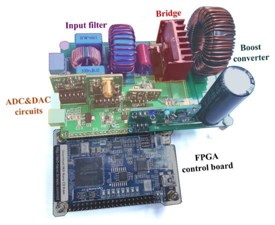
Figure 11.
Experimental prototype.
The main specifications of the power stage are given in Table 1, and the detailed specifications of the prototype components are given in Table 2. Two ADC modules (LTC2314-14 from ADI) were used for voltage samplings. The line voltage is divided by the resistor network, converted by ADC, and then sent to the FPGA for feedforward calculations. The valley current shaping relies on detection of the iv,ref crossing, which is carried out by a DAC (TLV5616 from TI, Dallas, TX, USA), an inductor current sensor (40 mΩ sensing resistor, Shenzhen, China) and an analog comparator (TLV3501 from TI, Texas, USA). The DAC converts iv,ref to analog value, and the comparator detects the iv,ref crossing point to initiate a new switching cycle. All digital signals are processed by a FPGA board (Cyclone IV from ALTERA, San Jose, CA, USA). The power stage consists of an input filter, a full bridge and a boost converter. The boost converter adopts a 180 μF capacitor (450LXW180MEFR18X45) as the output capacitor. The core material of main inductor is FeSiAl (77083A7 from MAGNETICS, Phoenix, AZ, USA). The main power switch is GS66508T (650 V E-mode GaN HEMT) from GAN SYSTEMS, Ottawa, Canada and the power diode is STPSC8H065 (650V SiC Schottky diode) from ST Microelectronics, Geneva, Switzerland.

Table 2.
Detailed specifications of components.
Table 1.
Main specifications of the prototype.
Table 1.
Main specifications of the prototype.
| Input voltage vin | 85–265 VAC |
| Output voltage vout | 400 VDC |
| Maximum power Pin | 280 W @ 110 VAC, 680 W @ 220 VAC |
| Output capacitor C | 180 μF |
| Boost inductor L | 350 μH |
| Fundamental switching cycle T | 10 μs |
| Input filter inductance Lf | 100 μH |
| Input filter capacitance Cf | 470 nF |
| Cg | 1 μF |
In the following, mode mixing is verified at different powers. Comparisons of different controls are given in the aspects of power range, current stress, power factor, THD and efficiency.
5.1. Mode Mixing with TACC Control at Full Power
With TACC control to achieve mixed-mode operation, the converter automatically switches among three operation modes in a half-line cycle. With 110 VAC/280 W and 220 VAC/680 W, the measured results are given by Figure 12a and Figure 12b, respectively.
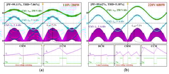
Figure 12.
Mode Mixing with TACC control. (a) 110 V/280 W; (b) 220 V/680 W.
According to (20), the mode mixing is dependent on F1,max = Vg/vout and F2 = 2LIref/(VgT) = 4LPin/(Vg2T). With 110 VAC/280 W, they were calculated as F1,max = 0.39 and F2 = 1.62. With the calculated values, the converter was expected to achieve mixed CRM/CCM operation, as indicated by Figure 12b. The measured results matched the expectation: the inductor current was CRM when the line voltage is low, and became CCM when the line voltage was high. With 220 VAC/680 W, F1,max and F2 were given by F1,max = 0.78 and F2 = 0.98; thus, the converter would be expected to achieve mixed DCM/CRM/CCM operation. The measured result also matches with the expectation, where the inductor current switches among three modes in a half-line cycle. The PF and THD were measured as [PF = 99.11%, THD = 7.06%] under 110 VAC/280 W, and as [PF = 99.62%, THD = 5.18%] under 220 VAC/680 the.
It is noted that the input current waveforms in Figure 12 have some zero-crossing distortion (a.k.a. cusp distortion). For different control strategies, the distortion is conventionally caused by <1> erroneous CCM control law when the converter is forced to operate in DCM, <2> negative current effect near zero-crossing, <3> modulation error under narrow switching pulse, or <4> line capacitor and full-bridge. For TACC control, issues <1–3> are well-addressed, owing to the integration of DCM control law and the clamped frequency near zero-crossing. However, it still suffers from issue <4>, because it requires a relatively high line capacitor to provide smooth line voltage. This does not indicate that TACC is inferior to other control strategies in reducing zero-crossing distortion. For comparison: conventional CCM control (based on PWM) usually suffers from issue <1>, while conventional CRM control necessarily suffers from issues <2–4>, owing to the high current ripple and high switching frequency near zero-crossing, and conventional DCM control also suffers from issue <4>, owing to the high current ripple that increases the line capacitor.
5.2. Measured Waveforms with TACC Control at Different Voltages and Powers
With TACC control to regulate the inductor current average value, the waveforms were measured at different voltages and powers. Specifically, the operation points were set at typical low power (110 V/40 W & 220 V/80 W) and half power (110 V/140 W & 220 V/340 W). According to the analyses in Section 3.2, the mode mixing was determined by F1,max and F2.
At typical low power, the measured results are given by Figure 13. For 110 VAC/40 W, F1,max and F2 were calculated by 0.39 and 0.23, respectively. With 220 VAC/80 W, F1,max and F2 were calculated by 0.78 and 0.12, respectively. For both conditions, since F1,max < 1-F2, the TACC controller achieved single DCM operation, which matched with the results in Figure 13. However, the input current was a little distorted, as shown in Figure 13b. The reason for this was the delay (in VCS module) in resetting eRAMP. As a result, the PF and THD were measured as [PF = 98.76%, THD = 5.39%] and [PF = 95.58%, THD = 8.22%], respectively.
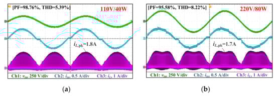
Figure 13.
Waveforms at low power. (a) 110 V/40 W; (b) 220 V/80 W.
The measured results at half power are given by Figure 14. For 110 VAC/140 W, F1,max and F2 were calculated by 0.39 and 0.81, respectively. Since , the TACC controller achieved mixed DCM/CRM operation. For 220 VAC/340 W, F1,max and F2 were calculated by 0.78 and 0.49, respectively. Since and F2 < 1, the TACC controller achieved mixed DCM/CRM/CCM operation.
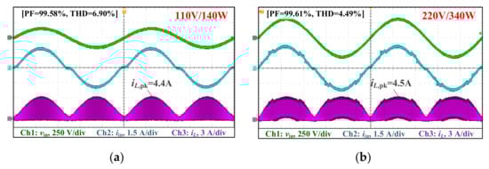
Figure 14.
Waveforms at half power. (a) 110 V/140 W; (b) 220 V/340 W.
The results in Figure 14 matched with the expectation, where partial CCM occurred at 220 V/340 W. The DCM operation was located near the zero-crossing point of input voltage. This alleviated the zero-crossing distortion by reducing variations of on/off times and switching cycle. Finally, for these operation points, the PF and THD were measured as [PF = 99.58%, THD = 6.90%] and [PF = 99.61%, THD = 4.49%], respectively.
5.3. Dynamic Response and Harmonic Analysis
With TACC control to regulate the inductor current average value, the dynamic responses were measured and are presented in Figure 15. During the positive load step (200 W to 400 W), the output voltage changed with an undershoot of 10.1% and recovered in 60 ms. During the negative load step (400 W to 200 W), an overshoot of 10.6% occurred and the recovery time was 100 ms.
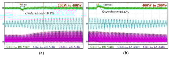
Figure 15.
Dynamic responses under load steps (a) from 200 W to 400 W; (b) from 400 W to 200 W.
To determine whether the converter with TACC control complied with the standard harmonic specifications, Figure 16 provides the harmonic comparisons with the IEC 61000-3-2 standard over a wide operating range (40–280 W under 110 V, 80–680 W under 220 V). All harmonic components of the input current were well below IEC 61000-3-2 standard, which indicates that the TACC control can adapt a wide operating range.
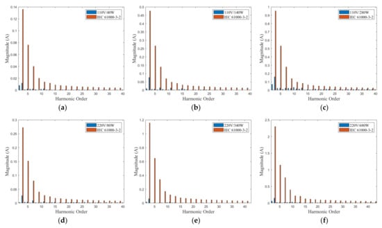
Figure 16.
Harmonic spectrums of input current compared with IEC 61000-3-2 standard. (a) 110 VAC/40 W; (b) 110 VAC/140 W; (c) 110 VAC/280 W; (d) 220 VAC/80 W; (e) 220 VAC/340 W; (f) 220 VAC/680 W.
5.4. Comprehensive Comparisons with Other Controls
Comprehensive comparisons with other controls were carried out in the aspects of current stress, power factor, THD and efficiency.
5.4.1. Current Stress
Compared with the single CRM operation, the mixed-mode control effectively reduced the maximum current stress by driving PFC converter into CCM at high line voltage and heavy load. The maximum iL,pk in a half-line cycle is measured in Figure 17. With CoT in the achievement of CRM, the maximum iL,pk changed heavily with the input power. With TACC control, variation of the maximum iL,pk was reduced. This matched with the previous analysis (Section 3.3) and simulations (Section 4.1). The reduced current stress allowed the converter to deliver higher power. Compared with CoT control, the TACC controller enlarged the maximum power with identical current stress. It enlarged the maximum power from 240 W to 280 W under 110VAC, and enlarged the power from 500 W to 680 W under 220 VAC.
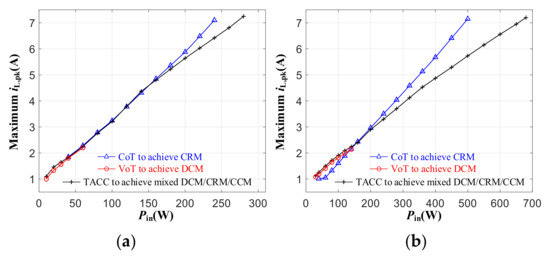
Figure 17.
Maximum iL,pk in a half-line cycle. (a) vin = 110 VAC; (b) vin = 220 VAC.
5.4.2. PF and THD
With different input voltage and power levels, the measured PF and THD are summarized in Figure 18 and Figure 19.
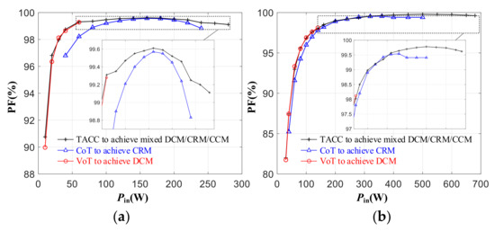
Figure 18.
Measured power factors. (a) vin = 110 VAC; (b) vin = 220 VAC.
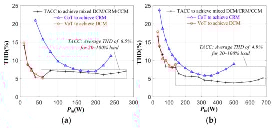
Figure 19.
Measured THDs. (a) vin = 110 VAC; (b) vin = 220 VAC.
For CoT to achieve CRM operation, the achieved PF and THD were degraded at both light and heavy loads. The degradation was evident when Pin was low, which was mainly caused by zero-crossing distortion. When Pin was high, the controller had enlarged switching cycle and current ripple, which also distorted the input current. For VoT to achieve DCM, the maximum input power was limited by the DCM boundary. For TACC control to achieve mixed-mode operation, it not only enlarged the power range, but also improved the PF and THD in the whole power range. When Pin changed from 20% to 100% of the maximum power, the achieved PF was always higher than 99.11% with 110 VAC, and higher than 98.02% with 220 VAC. In the range, the average PF was 99.45% with 110 VAC and 99.50% with 220 VAC. When Pin changed from 20% to 100% of the maximum power, the average THD was 6.5% with 110 VAC and 4.9% with 220 VAC.
5.4.3. Efficiency
The measured efficiencies with different controls are plotted in Figure 20. When the power level was low, the TACC controller had the highest efficiency. Compared with VoT in achieving DCM, it achieved valley switching, which reduced the switching losses of power switch and diode. Compared with CoT in achieving CRM, it reduced the switching frequency, which also reduced the switching loss. When the power level was high, the efficiency with CoT fell faster than that with TACC control. The reason mainly lay in the high current ripple and current stress, which greatly increased the conduction loss at high power.
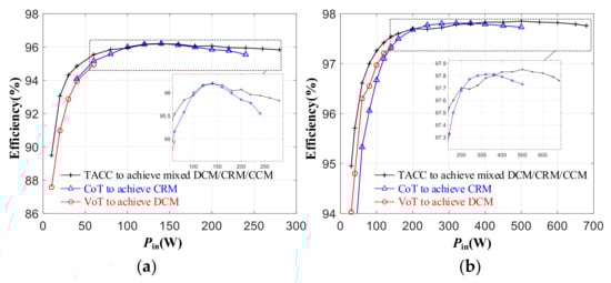
Figure 20.
Measured efficiencies (a) with 110 VAC input; (b) with 220 VAC input.
With 220 VAC input, the loss breakdowns with different controls were carried out under 80 W and 500 W, respectively. Equations for the loss breakdown are provided in Appendix A. As shown in Figure 21, the TACC control had the lowest total loss under 80 W, since it effectively reduced the GaN HEMT switching loss and the diode loss. Under 500 W, the TACC also reduced the total loss, since it lowered the inductor and rectifier bridge losses. This was achieved by partial CCM operation, which reduced the current ripple and current stress.
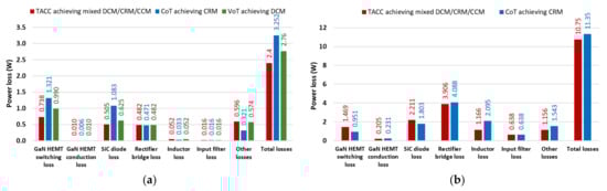
Figure 21.
Loss breakdown with 220 VAC input (a) under 80 W; (b) under 500 W.
Finally, Table 3 compares the performance of the proposed TACC control with other literature. Through mixed DCM/CRM/CCM operation and valley switching, the proposed TACC controller extended the preferable power range (efficiency > 95%, PF > 97%, THD < 10%). It suits PFC applications with wide input voltage and power ranges.
Table 3.
Comparisons with other controls.
Since multi-mode is universal for switching power converters, the proposed method has the potential to be extended to other topologies, such as half-bridge doubler boost [33], to broaden the operating range and improve the comprehensive performance.
6. Conclusions
This paper proposes a TACC control strategy to achieve mixed DCM/CRM/CCM operation for a boost PFC converter. The mixed-mode operation effectively extends the power range, since it reduces the current stress and variations of on/off times with input power. The proposed strategy accordingly incorporates DCM/CRM/CCM control algorithms to regulate the inductor current average value, which is realized with simple comparisons and valley current shaping. To make the algorithms compatible, design rules and normalized analyses are provided with respect to the operation regions and DCM/CRM/CCM boundaries. According to the simulation and experimental results, the inductor current peak value with TACC control is greatly reduced, which enables a higher operation range. Furthermore, owing to the reduced variations of on/off times and switching cycle, it improves the PF and THD within the whole power range.
Author Contributions
Conceptualization, Q.Z., R.M. and Q.T.; methodology, R.M. and L.L.; validation, L.L., G.S., H.X., J.Y. and N.L.; investigation, R.M. and Q.T.; writing—original draft preparation, L.L., G.S. and R.M.; writing—review and editing, H.X.; supervision, Q.Z. and Q.T. All authors have read and agreed to the published version of the manuscript.
Funding
This research was funded by the National Natural Science Foundation of China under Grant 62074067 and supported by the Ministry of Industry and Information Technology of the People’s Republic of China.
Acknowledgments
The authors would like to thank all the anonymous reviewers for their valuable suggestions to improve this work.
Conflicts of Interest
The authors declare no conflict of interest. The funders had no role in the design of the study; in the collection, analyses, or interpretation of data; in the writing of the manuscript, or in the decision to publish the results.
Appendix A
For boost PFC converter, the dominating power losses are listed in Table A1.
Table A1.
Dominating power losses in the converter.
Table A1.
Dominating power losses in the converter.
| Switching loss of power switch | |
| Conduction loss of power switch | |
| Switching losses of the diode | |
| Conduction loss of the boost diode | |
| Conduction loss of inductor | |
| Conduction loss of the full-bridge | |
| Conduction loss of the input filter |
For each aspect of the losses, equations for loss breakdown are given by (A1).
Relevant control variables are determined by the control strategies, and they are summarized in Table A2.
Table A2.
Variables with different controls.
Table A2.
Variables with different controls.
| TACC to Achieve Mixed DCM/CRM/CCM Operation | CoT to Achieve CRM | VoT to Achieve DCM | |||
|---|---|---|---|---|---|
| CCM | CRM | DCM | |||
| 0 | 0 | 0 | 0 | ||
In (A1), fs is the switching frequency, tR is the switch voltage rising time of the power switch, tF is the switch voltage falling time of the power switch, Tline is the line cycle, vsw,on is the switching node voltage when it is turned on, iL,valley and iL,peak are the valley and peak values of inductor current, Rds,on is the on resistance of the power switch, RF and VF are the forward resistance and voltage of the diode, RL is the equivalent series resistor of the inductor, RF,FB and VF,FB are the forward resistance and voltage of the bridge diode and RL,filter is the equivalent series resistor of the input filter.
Appendix B
In order to suppress exogenous noise and meet EMI requirements, an input LC filter is incorporated between the grid voltage and boost PFC converter. A schematic of the input LC filter is provided in Figure A1 consisting of a common mode (CM) filter and a differential mode (DM) filter. The CM filter is two coils wound on a core with the same winding direction to choke the CM current. The DM filter is a Π-type LC network to filter out the high frequency noise in differential mode. In addition to the LC filter, a capacitor (Cg) is added after the full bridge to reduce the voltage ripple of line voltage.

Figure A1.
The schematic of input LC filter.
Compared with single DCM and CRM operations, the proposed TACC control can reduce the requirements of the input filter. The reason lies in the reduced current ripple at high line voltage and heavy load, which is achieved by partial CCM operation.
Appendix C
In the prototype, the voltage loop is feedback from a PI compensator. In order to provide a constant Iref during the half-line period, the PI output is sampled and held every half-line cycle, which can be modeled as a zero-order holder function in frequency domain. Furthermore, the open loop transfer function, considering the PI compensator, sample gain and zero-order holder is
where ksample in the experiment prototype is 0.008, and Tzoh is half of the line cycle (i.e., 0.01 s). Furthermore, with tradeoff between response speed and stability, the PI parameters are tuned as kP = 3.18 and kI = 66.3. Finally, the simulated bode plot is given by Figure A2.

Figure A2.
Bode plot of the voltage loop.
The achieved phase margin is 74.4 degrees, which is high enough for stability. The cross-over frequency is 54.3 rad/s, which is consistent with the response time in Figure 15.
References
- Liu, X.; Li, X.; Zhou, Q.; Xu, J. Flicker-Free Single-Switch Quadratic Boost LED Driver Compatible with Electronic Transformers. IEEE Trans. Ind. Electron. 2019, 66, 3458–3467. [Google Scholar] [CrossRef]
- Tayar, T.; Abramovitz, A.; Shmilovitz, D. DCM Boost PFC for High Brightness LED Driver Applications. Energies 2021, 14, 5486. [Google Scholar] [CrossRef]
- Aamir, M.; Ullah Tareen, W.; Ahmed Kalwar, K.; Ahmed Memon, M.; Mekhilef, S. A High-Frequency Isolated Online Uninterruptible Power Supply (UPS) System with Small Battery Bank for Low Power Applications. Energies 2017, 10, 418. [Google Scholar] [CrossRef]
- Maciel, R.S.; de Freitas, L.C.; Coelho, E.A.A.; Vieira, J.B.; de Freitas, L.C.G. Front-End Converter with Integrated PFC and DC–DC Functions for a Fuel Cell UPS with DSP-Based Control. IEEE Trans. Power Electron. 2015, 30, 4175–4188. [Google Scholar] [CrossRef]
- Baek, J.; Park, M.-H.; Kim, T.; Youn, H.-S. Modified Power Factor Correction (PFC) Control and Printed Circuit Board (PCB) Design for High-Efficiency and High-Power Density On-Board Charger. Energies 2021, 14, 605. [Google Scholar] [CrossRef]
- Meher, S.R.; Banerjee, S.; Vankayalapati, B.T.; Singh, R.K. A Reconfigurable On-Board Power Converter for Electric Vehicle with Reduced Switch Count. IEEE Trans. Veh. Technol. 2020, 69, 3760–3772. [Google Scholar] [CrossRef]
- Yao, K.; Hu, W.; Li, Q.; Lyu, J. A Novel Control Scheme of DCM Boost PFC Converter. IEEE Trans. Power Electron. 2015, 30, 5605–5615. [Google Scholar] [CrossRef]
- Yao, K.; Li, L.; Tang, H.; Mao, C.; Chen, K. Optimum Boundary Inductance Control Concerning Limited PF for a DCM Boost PFC Converter. IEEE Trans. Power Electron. 2020, 35, 443–454. [Google Scholar] [CrossRef]
- Li, L.; Zhang, Q.; Min, R.; Liu, K.; Tong, Q.; Lyu, D. A Current Reshaping Strategy to Reduce Parasitics-Induced Current Distortion in Discontinuous Conduction Mode Boost Power Factor Correction Converter. IEEE Trans. Ind. Electron. 2021, 68, 2215–2224. [Google Scholar] [CrossRef]
- Luo, H.; Xu, J.; Luo, Y.; Sha, J. A Digital Pulse Train Controlled High Power Factor DCM Boost PFC Converter Over a Universal Input Voltage Range. IEEE Trans. Ind. Electron. 2019, 66, 2814–2824. [Google Scholar] [CrossRef]
- Yao, K.; Meng, Q.; Bo, Y.; Hu, W. Three-Phase Single-Switch DCM Boost PFC Converter with Optimum Utilization Control of Switching Cycles. IEEE Trans. Ind. Electron. 2016, 63, 60–70. [Google Scholar] [CrossRef]
- Gritti, G. Improvement of constant-on-time control for transition mode PFC Boost pre-regulators. In Proceedings of the 2020 IEEE Applied Power Electronics Conference and Exposition (APEC), New Orleans, LA, USA, 15–19 March 2020; pp. 1268–1272. [Google Scholar]
- Liu, X.; Zhang, D.; Wang, W.; Zhang, F.; Yuan, J.; Liu, N. Adaptive Charge-Compensation-Based Variable On-Time Control to Improve Input Current Distortion for CRM Boost PFC Converter. Energies 2022, 15, 4021. [Google Scholar] [CrossRef]
- Ren, X.; Guo, Z.; Wu, Y.; Zhang, Z.; Chen, Q. Adaptive LUT-Based Variable On-Time Control for CRM Boost PFC Converters. IEEE Trans. Power Electron. 2018, 33, 8123–8136. [Google Scholar] [CrossRef]
- Ren, X.; Wu, Y.; Guo, Z.; Zhang, Z.; Chen, Q. An Online Monitoring Method of Circuit Parameters for Variable On-Time Control in CRM Boost PFC Converters. IEEE Trans. Power Electron. 2019, 34, 1786–1797. [Google Scholar] [CrossRef]
- Ren, X.; Wu, Y.; Zhang, Z.; Chen, Q. Accurate Operation Analysis Based Variable On-time Control for 360–800 Hz CRM Boost PFC Converters. IEEE Trans. Ind. Electron. 2020, 67, 6845–6853. [Google Scholar] [CrossRef]
- Ren, X.; Zhou, Y.; Guo, Z.; Wu, Y.; Zhang, Z.; Chen, Q. Analysis and Improvement of Capacitance Effects in 360–800 Hz Variable On-Time Controlled CRM Boost PFC Converters. IEEE Trans. Power Electron. 2020, 35, 7480–7491. [Google Scholar] [CrossRef]
- Wu, Y.; Ren, X.; Zhou, Y.; Chen, Q.; Zhang, Z. Dynamic AC Line Frequency Response Method for LUT-Based Variable On-Time Control in 360–800 Hz CRM Boost PFC Converter. IEEE Trans. Power Electron. 2021, 36, 6208–6212. [Google Scholar] [CrossRef]
- Nair, H.S.; Lakshminarasamma, N. A Computationally Simple Predictive CCM Average Current Controller with Nearly Zero Tracking Error for Boost PFC Converter. IEEE Trans. Ind. Appl. 2020, 56, 5083–5094. [Google Scholar] [CrossRef]
- Wang, W.; Shen, G.; Min, R.; Tong, Q.; Zhang, Q.; Liu, Z. State Switched Discrete-Time Model and Digital Predictive Voltage Programmed Control for Buck Converters. Energies 2020, 13, 3451. [Google Scholar] [CrossRef]
- Luo, H.; Xu, J.; He, D.; Sha, J. Pulse Train Control Strategy for CCM Boost PFC Converter with Improved Dynamic Response and Unity Power Factor. IEEE Trans. Ind. Electron. 2020, 67, 10377–10387. [Google Scholar] [CrossRef]
- Franco de Souza, A.; Ribeiro, E.R.; Vicente, E.M.; Tofoli, F.L. Experimental evaluation of active power factor correction techniques in a single-phase AC-DC boost converter. Int. J. Circuit Theory Appl. 2019, 47, 1529–1553. [Google Scholar] [CrossRef]
- Ren, X.; Zhou, Y.; Guo, Z.; Wu, Y.; Zhang, Z.; Chen, Q. Simple Analog-Based Accurate Variable On-Time Control for Critical Conduction Mode Boost Power Factor Correction Converters. IEEE J. Emerg. Sel. Top. Power Electron. 2020, 8, 4025–4036. [Google Scholar] [CrossRef]
- Zhang, Y.; Yao, C.; Zhang, X.; Chen, H.; Li, H.; Wang, J. Power Loss Model for GaN-Based MHz Critical Conduction Mode Power Factor Correction Circuits. IEEE J. Emerg. Sel. Top. Power Electron. 2020, 8, 141–151. [Google Scholar] [CrossRef]
- Clark, C.; Eberle, W.; Musavi, F. An Adaptive Digital Controller for the Mixed Conduction Mode Boost Power Factor Correction Converter. In Proceedings of the 2013 Twenty-Eighth Annual IEEE Applied Power Electronics Conference and Exposition (APEC), Long Beach, CA, USA, 17–21 March 2013; pp. 2712–2719. [Google Scholar]
- Clark, C.W.; Musavi, F.; Eberle, W. Digital DCM Detection and Mixed Conduction Mode Control for Boost PFC Converters. IEEE Trans. Power Electron. 2014, 29, 347–355. [Google Scholar] [CrossRef]
- Fernandes, R.; Trescases, O. A Multimode 1-MHz PFC Front End with Digital Peak Current Modulation. IEEE Trans. Power Electron. 2016, 31, 5694–5708. [Google Scholar] [CrossRef]
- Nair, H.S.; Narasamma, N.L. An Improved Digital Algorithm for Boost PFC Converter Operating in Mixed Conduction Mode. IEEE J. Emerg. Sel. Top. Power Electron. 2020, 8, 4235–4245. [Google Scholar] [CrossRef]
- Chen, Z.; Xu, J.; Davari, P.; Wang, H. A Mixed Conduction Mode-Controlled Bridgeless Boost PFC Converter and Its Mission Profile-Based Reliability Analysis. IEEE Trans. Power Electron. 2022, 37, 9674–9686. [Google Scholar] [CrossRef]
- Tripathi, R.K.; Das, S.P.; Dubey, G.K. Mixed-mode operation of boost switch-mode rectifier for wide range of load variations. IEEE Trans. Power Electron. 2002, 17, 999–1009. [Google Scholar] [CrossRef]
- Yao, K.; Wu, C.; Chen, J.; Yang, J.; Li, J.; Jin, Z.; Wang, S.; Yang, R.; Liu, L.; Gao, Y.; et al. A Scheme to Improve Power Factor and Dynamic Response Performance for CRM/DCM Buck-Buck/Boost PFC Converter. IEEE Trans. Power Electron. 2020, 36, 1828–1843. [Google Scholar] [CrossRef]
- Chen, Y.; Chen, Y. Line Current Distortion Compensation for DCM/CRM Boost PFC Converters. IEEE Trans. Power Electron. 2016, 31, 2026–2038. [Google Scholar] [CrossRef]
- Neto, R.M.F.; Tofoli, F.L.; de Freitas, L.C. A High-Power-Factor Half-Bridge Doubler Boost Converter without Commutation Losses. IEEE Trans. Ind. Electron. 2005, 52, 1278–1285. [Google Scholar] [CrossRef]
Publisher’s Note: MDPI stays neutral with regard to jurisdictional claims in published maps and institutional affiliations. |
© 2022 by the authors. Licensee MDPI, Basel, Switzerland. This article is an open access article distributed under the terms and conditions of the Creative Commons Attribution (CC BY) license (https://creativecommons.org/licenses/by/4.0/).