
ULP Super Regenerative Transmitter with Digital Quenching Signal Controller


Abstract
:
1. Introduction
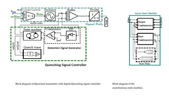
2. Proposed Regenerative Transmitter Block Diagram
3. Signal Path Circuit Design
3.1. Bias Current Control
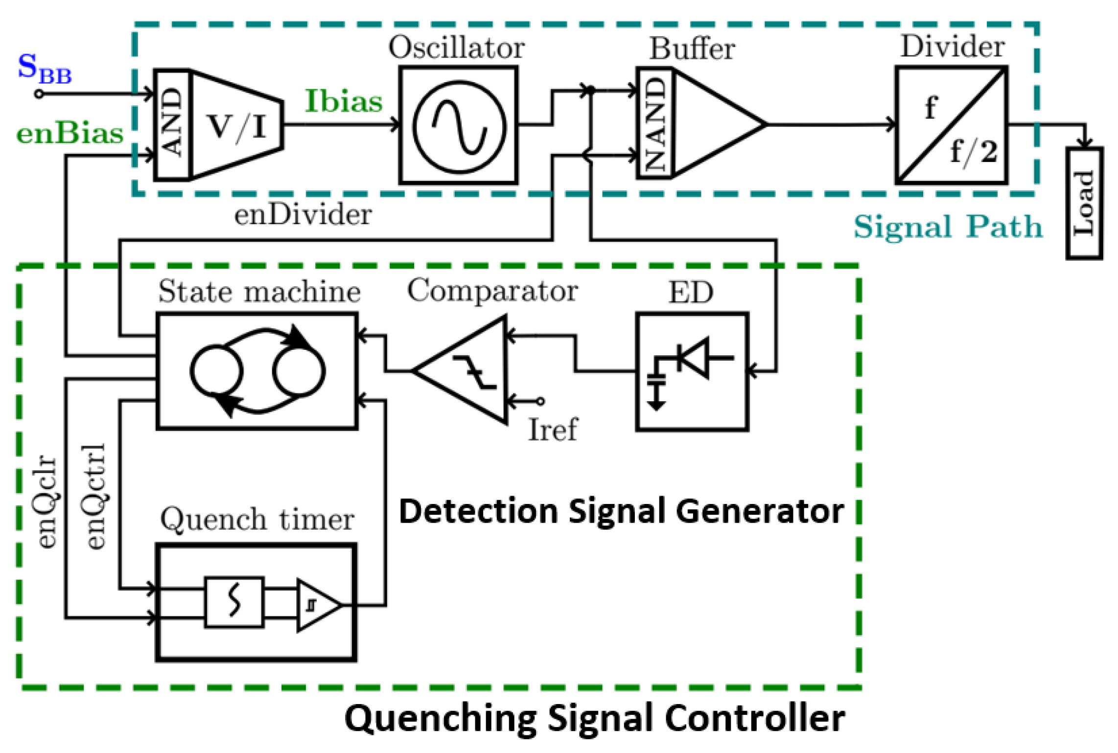
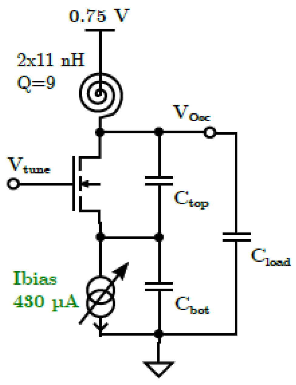
3.2. Oscillator
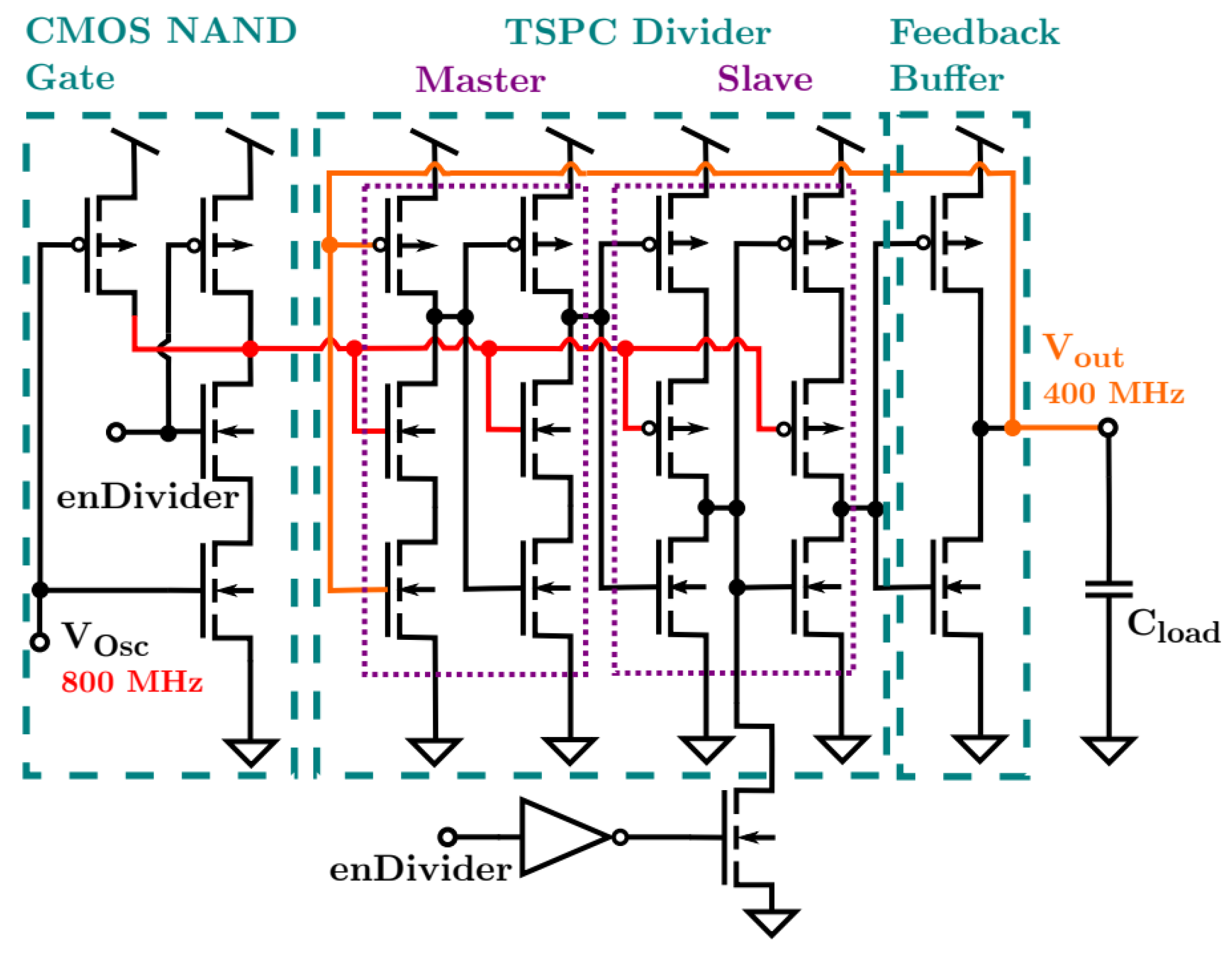
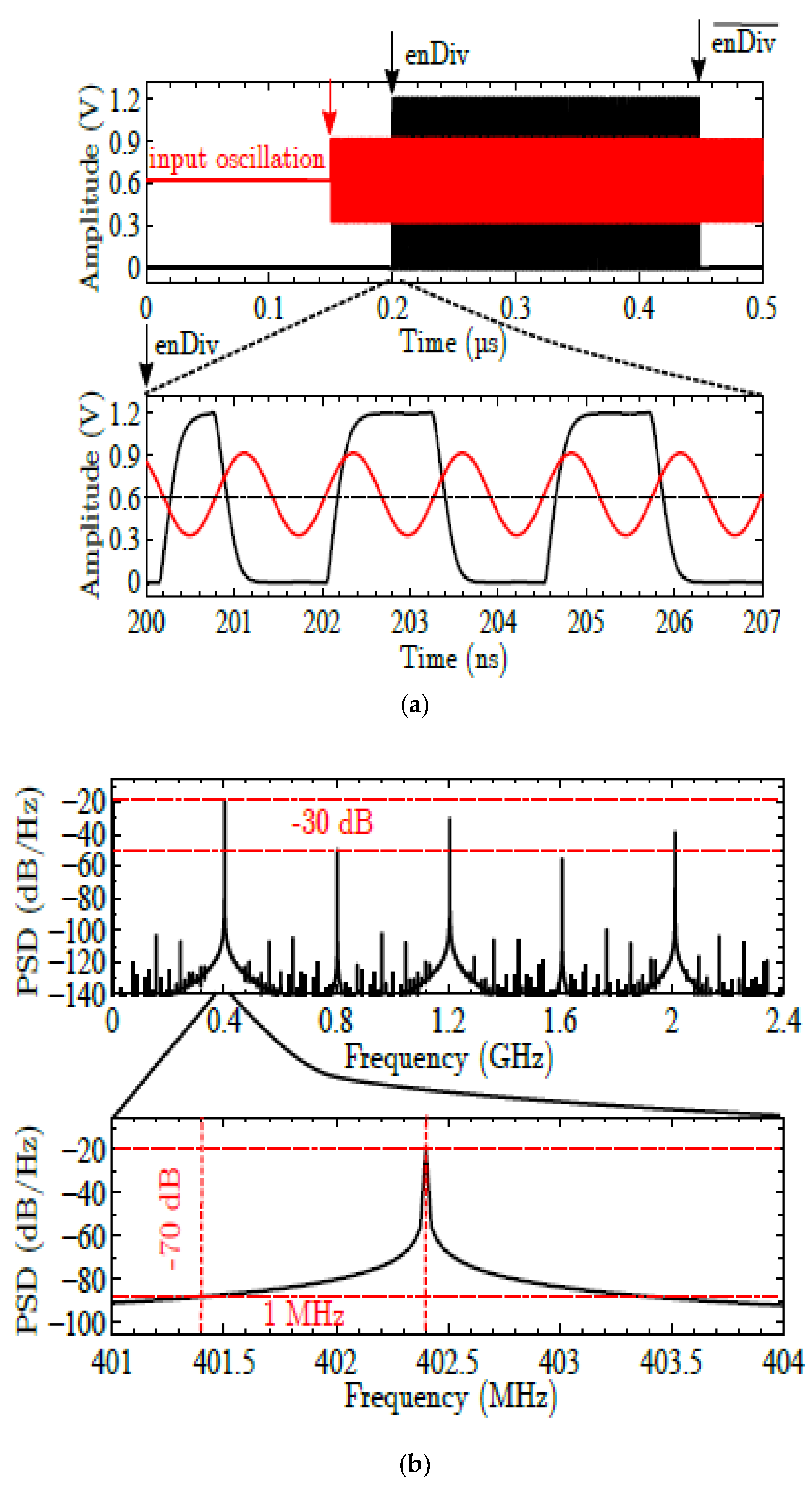
3.3. Frequency Divider
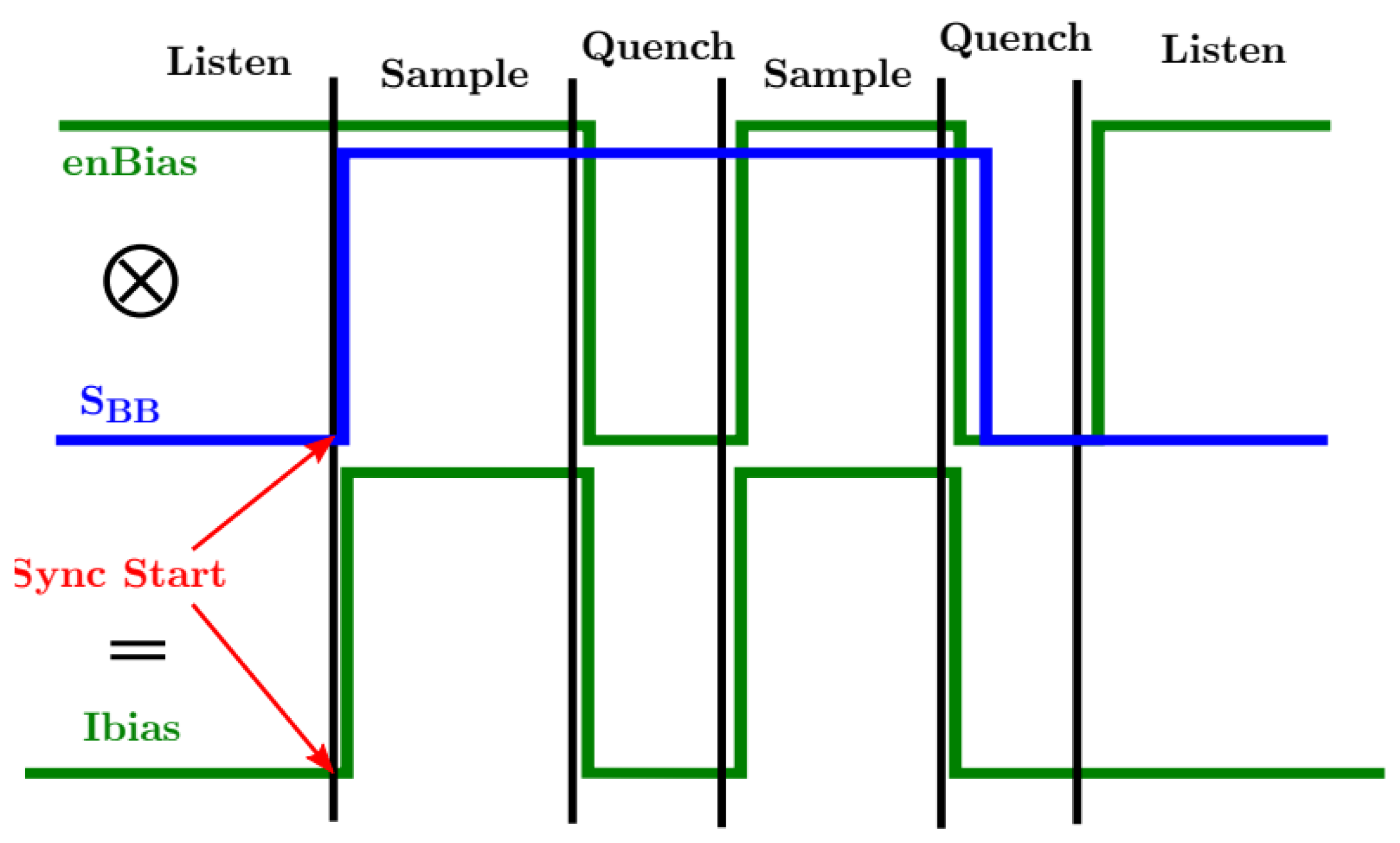
4. Quenching Signal Controller
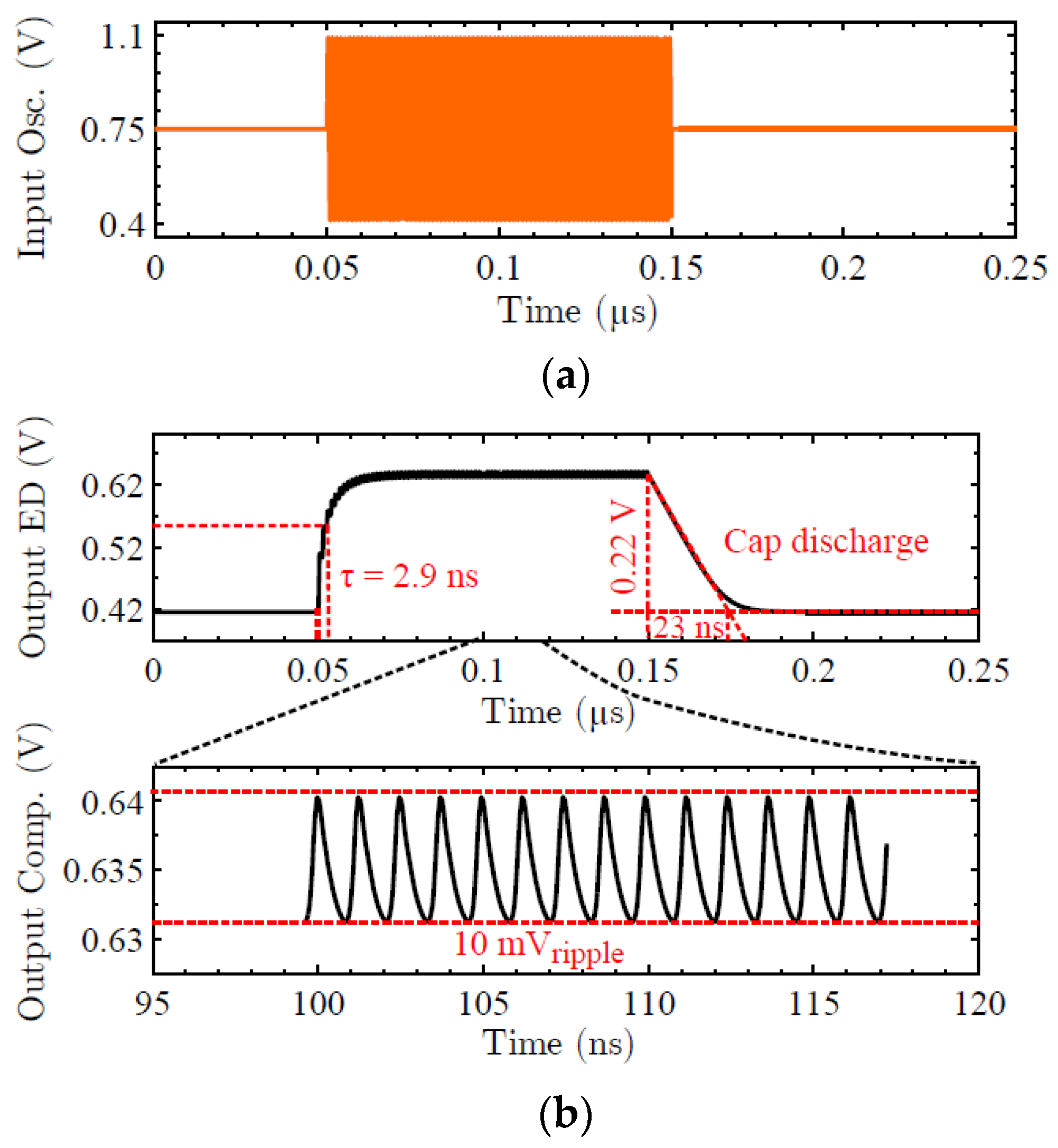
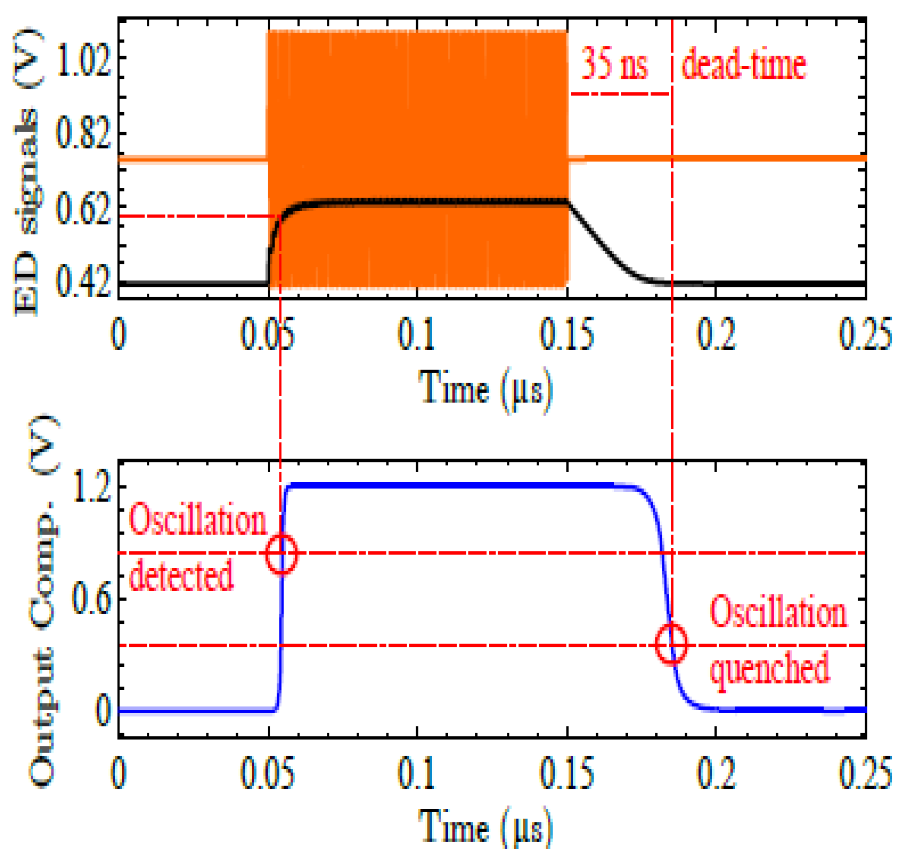
4.1. Envelope Detector
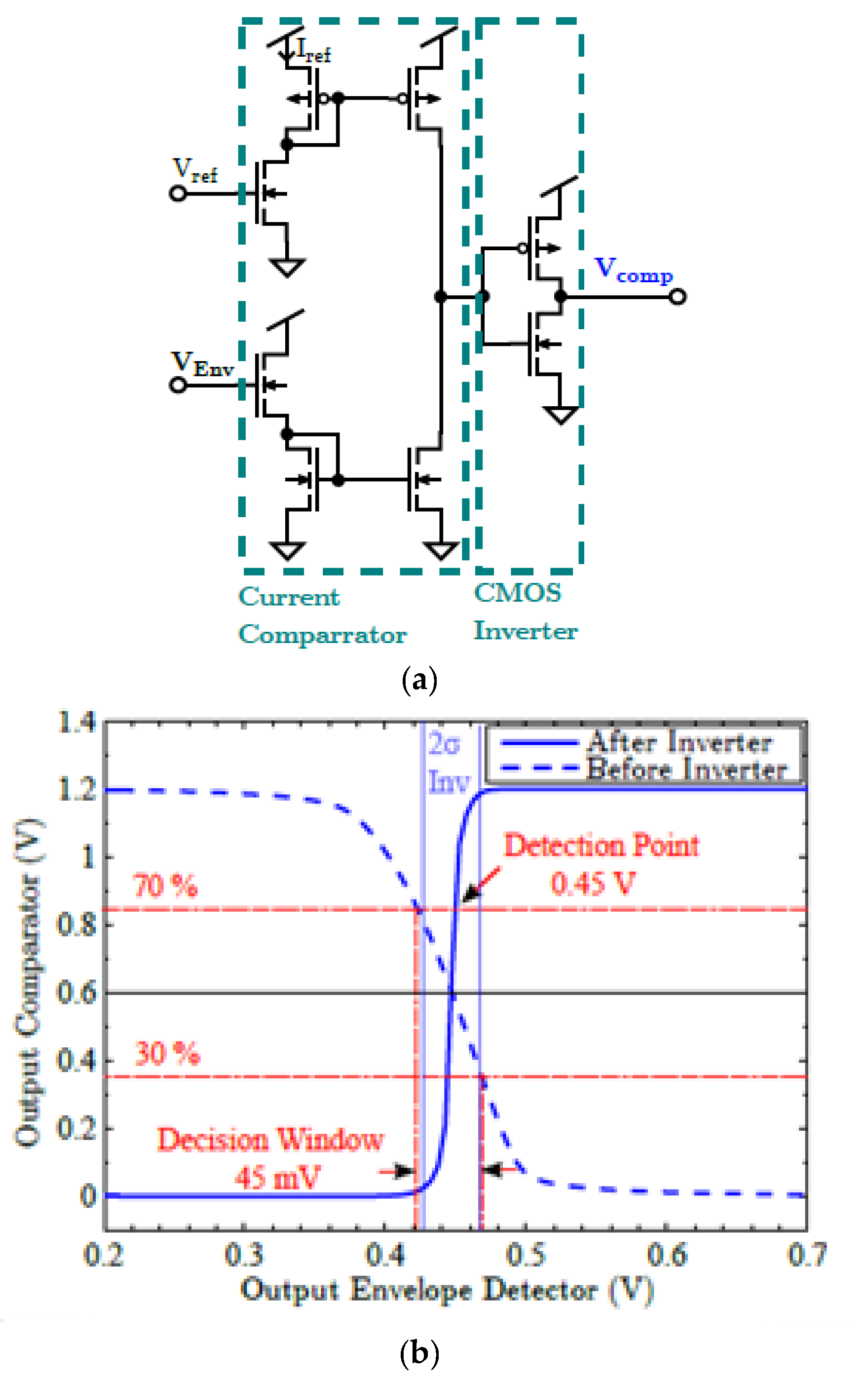
4.2. Comparator
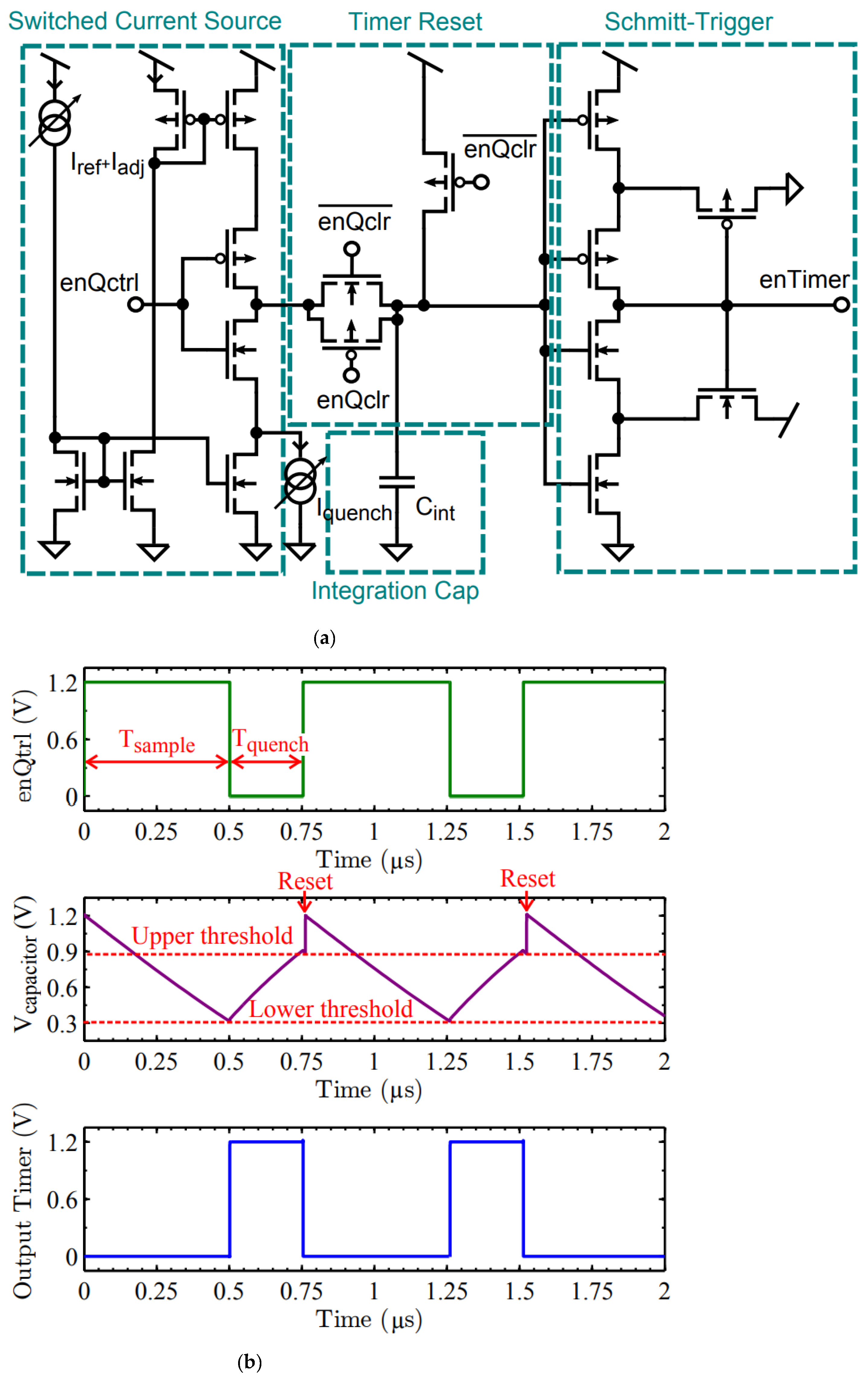
4.3. Quench Timer
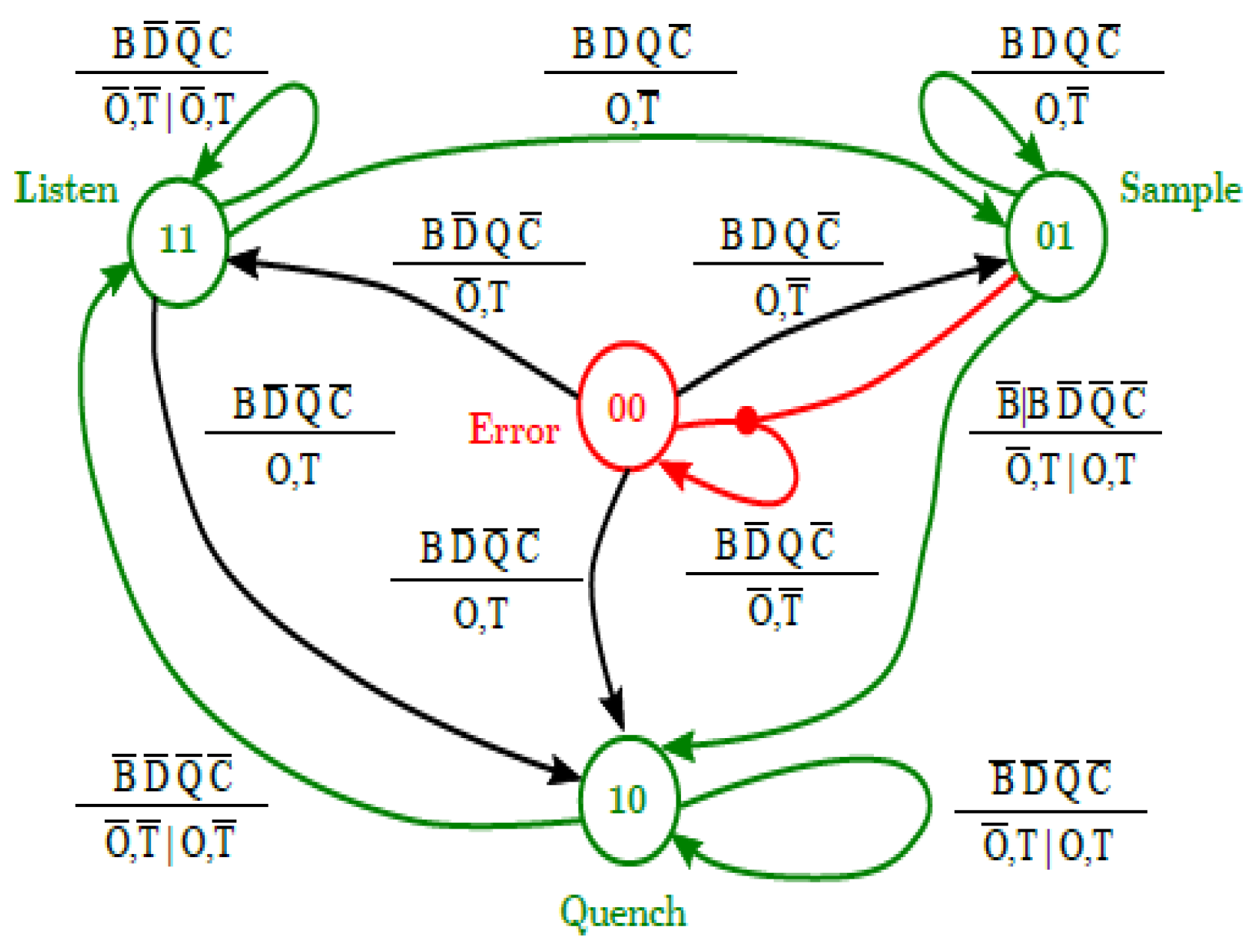
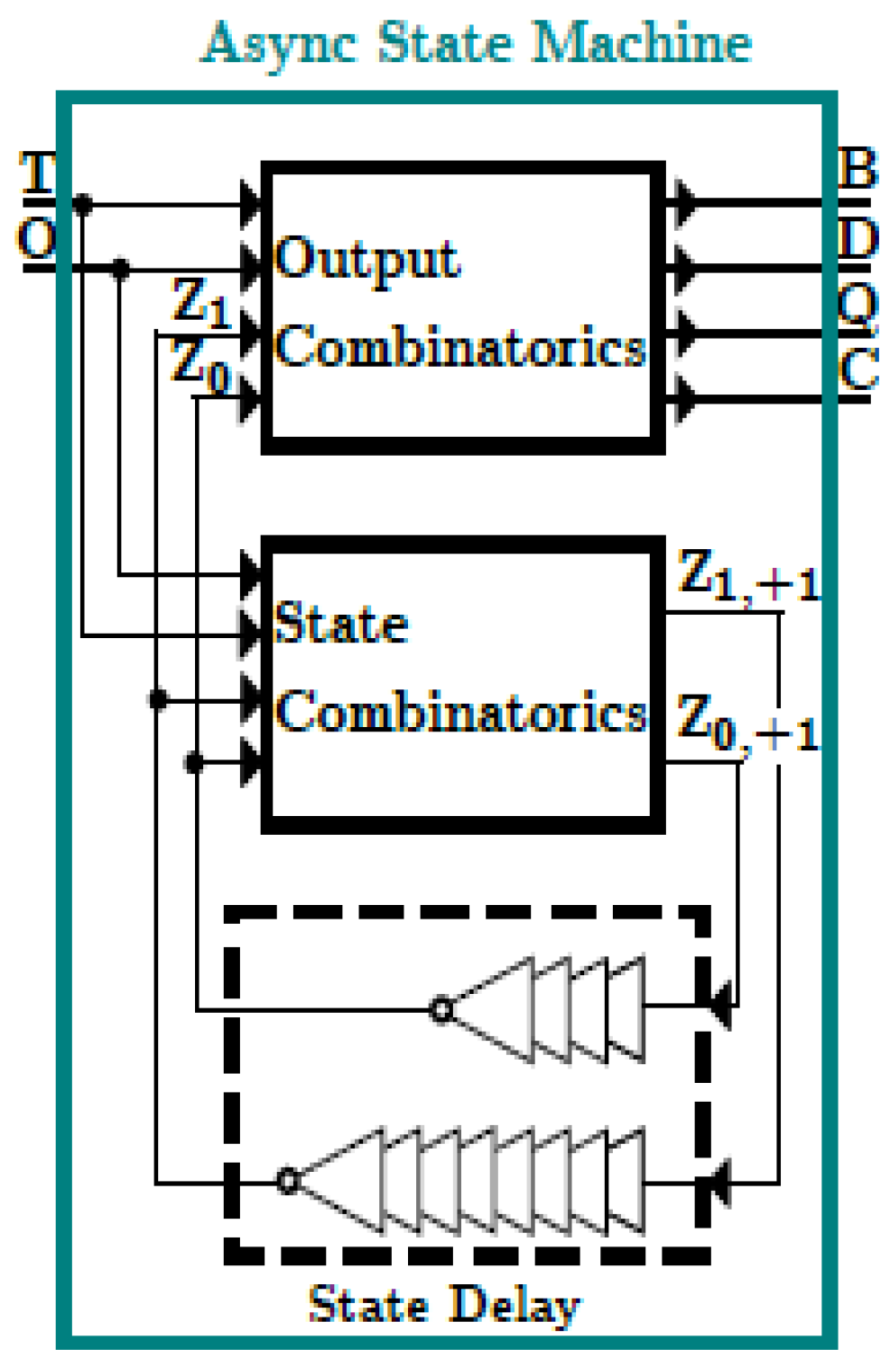
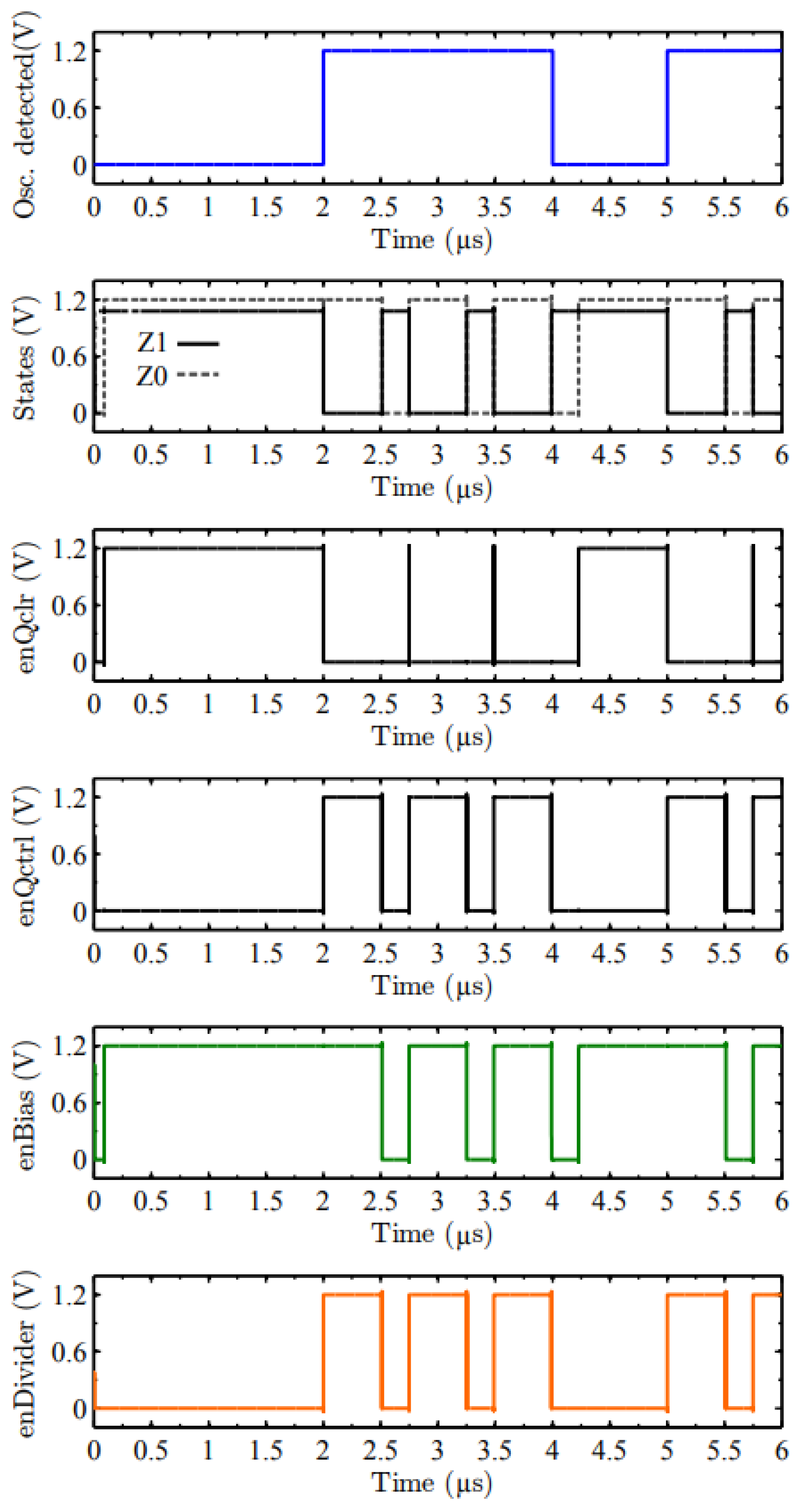
4.4. State Machine
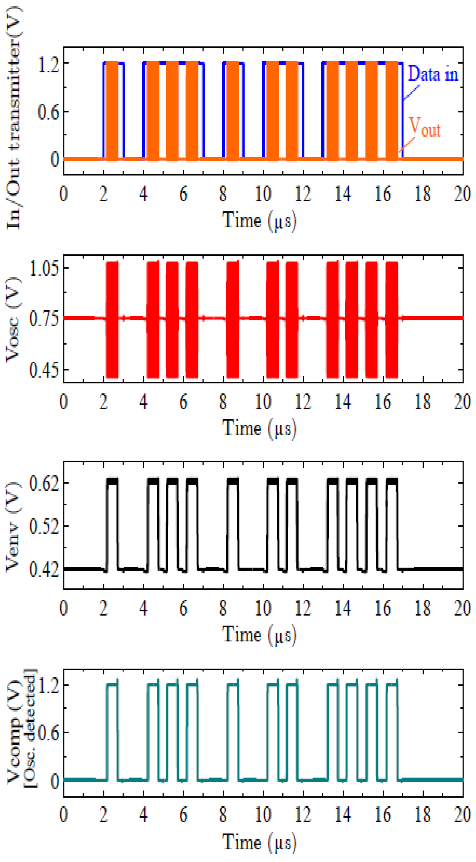
5. System Performance
6. Conclusions
Author Contributions
Funding
Conflicts of Interest
References
- Peruzzi, G.; Pozzebon, A. A Review of Energy Harvesting Techniques for Low Power Wide Area Networks (LPWANs). Energies 2020, 13, 3433. [Google Scholar] [CrossRef]
- Motlagh, N.H.; Mohammadrezaei, M.; Hunt, J.; Zakeri, B. Internet of Things (IoT) and the Energy Sector. Energies 2020, 13, 494. [Google Scholar] [CrossRef]
- Rong, G.; Zheng, Y.; Sawan, M. Energy Solutions for Wearable Sensors: A Review. Sensors 2021, 21, 3806. [Google Scholar] [CrossRef]
- Shawkey, H.; Elsheakh, D. Multiband Dual-Meander Line Antenna for Body-Centric Networks’ Biomedical Applications by Using UMC 180 nm. Electronics 2020, 9, 1350. [Google Scholar] [CrossRef]
- Liu, H.; Zhu, X.; Boon, C.; Yi, X.; Kong, L. A 71 dB 150µW Variable-Gain Amplifier in 0.18 µm CMOS Technology. IEEE Microw. Wirel. Compon. Lett. 2015, 25, 334–336. [Google Scholar] [CrossRef]
- Garcia-Alberdi, C.; Aguado-Ruiz, J.; Lopez-Martin, A.; Ramirez-Angulo, J. Micro-power class-AB VGA with gain-independent bandwidth. IEEE Trans. Circuits Syst. II Exp. Briefs 2013, 60, 397–401. [Google Scholar] [CrossRef]
- Elwan, H.; Tekin, A.; Pedrotti, K. A differential-ramp based 65 dB-linear VGA technique in 65 nm CMOS. IEEE J. Solid-State Circuits 2009, 44, 2503–2514. [Google Scholar] [CrossRef]
- Kang, S.Y.; Jang, J.; Oh, I.-Y.; Park, C.S. A 2.16 mW Low Power Digitally-Controlled Variable Gain Amplifier. IEEE Microw. Wirel. Compon. Lett. 2010, 20, 172–174. [Google Scholar] [CrossRef]
- Kang, S.-Y.; Ryu, S.-T.; Park, C.-S. A Precise Decibel-Linear Programmable Gain Amplifier Using a Constant Current-Density Function. IEEE Trans. Microw. Theory Tech. 2012, 60, 2843–2850. [Google Scholar] [CrossRef]
- Mostafa, M.; Embabi, S.; Elmala, M. A 60-dB 246-MHz CMOS variable gain amplifier for subsampling GSM receivers. In Proceedings of the International Symposium on Low Power Electronics and Design, Huntington Beach, CA, USA, 6–7 August 2001. [Google Scholar] [CrossRef]
- Duong, Q.; Le, Q.; Kim, C.; Lee, S. A 95-dB linear low-power variable gain amplifier. IEEE Trans. Circuits Syst. I Regul. Pap. 2006, 53, 1648–1657. [Google Scholar] [CrossRef]
- Rodríguez, T.; Galán, J.; Pedro, M.; Martin, A.; Carvajal, R.; Angulo, J. Low-power CMOS variable gain amplifier based on a novel tunable transconductor. IET Circuits Devices Syst. 2015, 9, 105–110. [Google Scholar] [CrossRef]
- Choi, I.; Seo, H.; Kim, B. Accurate dB-Linear Variable Gain Amplifier With Gain Error Compensation. IEEE J. Solid-State Circuits 2013, 48, 456–464. [Google Scholar] [CrossRef]
- Kalentediris, V.; Mountrichas, L.; Vlassis, S.; Siskos, S. A CMOS linear-in-dB VGA and agc loop for telecommunications applications. Microelectron. J. 2013, 44, 1063–1071. [Google Scholar] [CrossRef]
- Faraji-Baghtash, H.; Ayatollahi, A. A zero-pole reposition based, 0.95-mW, 68-dB, linear-in-dB, constant-bandwidth variable gain amplifier. Circuits Syst. Signal Process 2014, 33, 1353–1368. [Google Scholar] [CrossRef]
- Chen, Z.; Zheng, Y.; Choong, F.C.; Je, M. A Low-Power Variable-Gain Amplifier With Improved Linearity: Analysis and Design. IEEE Trans. Circuits Syst. I Regul. Pap. 2012, 59, 2176–2185. [Google Scholar] [CrossRef]
- Shuigen, H.; Min, L.; Ruoyu, W.; Zhuojun, C.; Yemin, D. A 400 MHz Single-Chip CMOS Transceiver for Long Range High Definition Video Transmissionin UAV Application. Chin. J. Electron. 2020, 29, 554–562. [Google Scholar]
- Pandey, J.; Brian Otis, B. A 90 μW MICS/ISM Band Transmitter with 22% Global Efficiency. In Proceedings of the 2010 IEEE Radio Frequency Integrated Circuits Symposium, Anaheim, CA, USA, 23–25 May 2010. [Google Scholar]
- Fu, Y.; Elsankary, K. A Low-Power, High-Sensitivity, OOK-Super-Regenerative Receiver for WBANs. IEEE Trans. Circuits Syst. II: Express Briefs 2019, 66, 793–797. [Google Scholar] [CrossRef]
- Razavi, B. RF Microelectronics, 2nd ed.; Prentice Hall Press: Hoboken, NJ, USA, 2012. [Google Scholar]
- Murtaza, C.; Cojan, R. Design and analysis of a low power consumption high speed frequency divider by 2/3. In Proceedings of the 2010 International Semiconductor Conference (CAS 2010), Sinaia, Romania, 11–13 October 2010; Volume 02, pp. 449–452. [Google Scholar]
- Karplayan, A.; Schaumann, R. Automatic Tuning of Frequency and Q-factor of Bandpass Filters Based on Envelope Detection. In Proceedings of the IEEE International Symposium on Circuits and Systems ISCAS ’98, Monterey, CA, USA, 31 May–3 June 1998. [Google Scholar]
- Hauck, S. Asynchronous design methodologies: An overview. Proc. IEEE 1995, 83, 69–93. [Google Scholar] [CrossRef]
- Ma, C.; Hu, C.; Cheng, J.; Xia, L.; Chiang, P. A Near-Threshold, 0.16 nJ/b OOK-Transmitter with 0.18 nJ/b Noise-Cancelling Super-Regenerative Receiver for the Medical Implant Communications Service. IEEE Trans. Biomed. Circuits Syst. 2013, 7, 841–850. [Google Scholar]
- Tajalli, A.; Leblebici, Y. Design Trade-offs in Ultra-Low-Power Digital Nanoscale CMOS. IEEE Trans. Circuits Syst. I Regul. Pap. 2011, 58, 2189–2200. [Google Scholar] [CrossRef]
- Lee, K.; Nam, I.; Kwon, I.; Gil, J.; Han, K.; Park, S.; Seo, B.-I. The Impact of Semiconductor Technology Scaling on CMOS RF and Digital Circuits for Wireless Application. IEEE Trans. Electron Devices 2005, 52, 1415–1422. [Google Scholar] [CrossRef]
- Cho, H.; Kim, H.; Kim, M.; Jang, J.; Lee, Y.; Lee, K.J.; Bae, J.; Yoo, H.J. A 79 pJ/b 80 Mb/s full-duplex transceiver and a 42.5 μW 100 kb/s super-regenerative transceiver for body channel communications. In Proceedings of the 2015 IEEE International Solid-State Circuits Conference—(ISSCC) Digest of Technical Papers, San Francisco, CA, USA, 22–26 February 2015; pp. 380–381. [Google Scholar]
- Vidojkovic, M.M.; Huang, X.; Harpe, P.P.; Rampu, S.; Zhou, C.; Huang, L.L.; Van De Molengraft, J.; Imamura, K.; Busze, B.; Bouwens, F.; et al. A 2.4 GHz ULP OOK Single-Chip Transceiver for Healthcare Applications. In Proceedings of the 2011 IEEE International Solid-State Circuits Conference, San Francisco, CA, USA, 20–24 February 2011. [Google Scholar]
- Ma, R.; El Agroudy, N.; Becker, M.; Joram, N.; Ellinger, F. A 401-406 MHz Wireless Transceiver Analogue Front-End for Medical Implantable Applications. In Proceedings of the 19th IEEE International New Circuits and Systems Conference (NEWCAS), Virtual, 13–16 June 2021. [Google Scholar]
- Zong, P.; Zhou, Y.; Zhang, H.; Zhou, Y.; Wang, K. A 433 MHz Transmitter Based on Injection-Locking and Frequency Multiplication. In Proceedings of the 2019 IEEE 4th International Conference on Integrated Circuits and Microsystems (ICICM), Beijing, China, 25–27 October 2019. [Google Scholar]


| Gate | State Logic | Output Logic | Inputs | Delay |
|---|---|---|---|---|
| NAND | 11 | 15 | 0 | 0 |
| NOT | 1 | 4 | 4 | 12 |
| Parameter | Carrier Freq. ( MHz) | Tuning Range ( MHz) | Max. input Data Rate (Mbps) | Max./Min Quench freq.( MHz) | Carrier PSD (dB/Hz) | Carrier 3rd Harm. (dB) | Oscill. Isolation (dB) | 1 MHz Prms (µW) |
|---|---|---|---|---|---|---|---|---|
| Sim. result | 402–405 | ±1 | 2 | 1/0.19 | −30 | −10 | −27 | 537 |
| Parameter | [17] | [18] | [24] | [27] | [28] | [29] | [30] | This Work |
|---|---|---|---|---|---|---|---|---|
| Freq. (MHz) | 402–405 | 400 | 402–405 | 13.56 | 2400 | 401–406 | 433 | 402–405 |
| Technology | 130 nm | 130 nm | 90 nm | 65 nm | 90 nm | 180 nm | 180 nm | 130 nm |
| Data rate | 54 Mbps | 200 Kbps | 1 Mbps | 100 Kbps | 100 Kbps | 1 Mbps | NA | 2 Mbps |
| Supply Voltage (V) | 1.2 | 1 | 0.6–1 | 0.8 | 1.8 | 1.8 | 1.2 | |
| Energy/bit | 1.2 nJ | 0.45 nJ | 0.16 nJ | 0.425 nJ | 23 nJ | NA | 0.27 nJ | |
| Power dissipation | 68.2 mW | 90 µW | 160 µW@0.6V | 42.5 µW | 2.53 mW | 23 mW | 580 µW | 537 µW |
Publisher’s Note: MDPI stays neutral with regard to jurisdictional claims in published maps and institutional affiliations. |
© 2022 by the authors. Licensee MDPI, Basel, Switzerland. This article is an open access article distributed under the terms and conditions of the Creative Commons Attribution (CC BY) license (https://creativecommons.org/licenses/by/4.0/).
Share and Cite
Kayed, S.; Saleh, S.; Shawkey, H. ULP Super Regenerative Transmitter with Digital Quenching Signal Controller. Energies 2022, 15, 7123. https://doi.org/10.3390/en15197123
Kayed S, Saleh S, Shawkey H. ULP Super Regenerative Transmitter with Digital Quenching Signal Controller. Energies. 2022; 15(19):7123. https://doi.org/10.3390/en15197123
Chicago/Turabian StyleKayed, Somaya, Sherif Saleh, and Heba Shawkey. 2022. "ULP Super Regenerative Transmitter with Digital Quenching Signal Controller" Energies 15, no. 19: 7123. https://doi.org/10.3390/en15197123
APA StyleKayed, S., Saleh, S., & Shawkey, H. (2022). ULP Super Regenerative Transmitter with Digital Quenching Signal Controller. Energies, 15(19), 7123. https://doi.org/10.3390/en15197123