Article

UTC Synchronized Signal Generation for Synchrophasors and Sampled Values Measurements

1
Łukasiewicz Research Network, Tele and Radio Research Institute, 03-450 Warsaw, Poland
2
Faculty of Electrical Engineering, Wroclaw University of Science and Technology, Wybrzeze Wyspianskiego St. 27, 50-370 Wroclaw, Poland
*
Author to whom correspondence should be addressed.
Energies 2022, 15(19), 7095; https://doi.org/10.3390/en15197095
Submission received: 13 September 2022 / Revised: 23 September 2022 / Accepted: 24 September 2022 / Published: 27 September 2022

Abstract

:
This article describes two methods and circuits for generation of a signal synchronized to the Coordinated Universal Time (UTC) time scale. The signal is used as a sampling clock for a synchrophasor and Sampled Values generation. Both methods use a PPS (Pulse Per Second) pulse as a synchronization signal. In the first method, the synchronization procedure is implemented entirely in a Field Programmable Gate Array (FPGA) device. The second method uses a microcontroller and a Temperature Compensated Voltage Controlled Crystal Oscillator (TCVCXO). The common feature of the presented methods is that they are cost effective and use a minimal number of components. This paper presents the implementation details of both methods as well as the measurement results, which show that the accuracy of the synchronized signals in both procedures makes them suitable for use in synchrophasors and sampled values measurements.

1. Introduction

Due to the increasing number of distributed renewable energy sources (RES), today’s power grids are becoming less predictable than traditional power networks, as the available power is dependent on atmospheric conditions. Moreover, the disturbances introduced by RES can lead to the island mode operation of the power network, and due to the balancing of energy generated by RES and the energy consumed, such a state can persist for a long time. Traditional protection and control devices are not adapted for island operation of the power grid [1,2]. Synchrophasor technology [3] is essentially the only method for analyze the dynamical behavior of power grids in real time and ensuring their stability under challenging conditions.
While synchrophasor technology has been almost exclusively used in high voltage networks [4,5,6,7], over the last several years, research has been carried out to use them in medium and low power networks [6,7,8,9,10]. The main factor restricting the use of synchrophasor technology is the high cost of Phasor Measurement Units (PMU), the devices used for synchrophasor determination. To make synchrophasor technology viable in medium and low power networks, it is necessary to develop cost effective solutions for synchrophasor determination, especially the generation and distribution of reference times and frequency signals. Moreover, the lower geographical extent of medium power networks compared to high voltage networks imposes more stringent condition on synchrophasor phase resolution, which translates into higher demands on the accuracy of the reference time and frequency signals needed to timestamp the synchrophasor values.
The growing complexity of power networks and increasing costs of traditional substation automation methods have led to the development and gradual adoption of the IEC 61850 standard [11,12,13]. One of the features of IEC 61850 is the concept of a process bus, in which line voltage and current values are published over an ethernet network in the form of digital Sampled Values (SV) that are timestamped with a reference time disciplined to UTC. The conversion of analog values to digital ones takes place in a device called a Merging Unit (MU). The SVs are used by Intelligent Electronic Devices (IED) connected to a process bus, such as a protective relay, to determine the current and voltage RMS values, power consumption, power factor, and other parameters that characterize the state of the power network. The accuracy of the estimation of parameters characterizing a power network depends on the accuracy of SV timestamping, as it is necessary to time-align voltage and current samples, and certain protection algorithms require the data from various part of the power network to be aligned.
In this paper, we describe two methods of providing a local reference time synchronized to the UTC timescale for use by PMUs and MUs to timestamp measurement values.
The rest of the paper is organized into several sections. In Section 2, related works and standards are analyzed. Section 3 presents detailed descriptions of the proposed devices and synchronization algorithms. Section 4 presents the experimental setup. Section 5 elaborates on the comprehensive analysis of measurement results, and Section 6 presents the conclusions.

2. Related Works and Standards

As concerns the PMU device, the synchrophasor accuracy, referred to as TVE [3,6], is related to the accuracy of the available synchronization signal used for time stamping. The relevant standard [3] demands that TVE should be within 1% of its true value. This means that if all the errors contributing to TVE error except for the timing error are left aside, the maximum allowable timing error at 50 Hz is ± 31.833 µs. In practice, the standard highly recommends that the timing error should be ten times lower to allow for other errors that may contribute to TVE, and should preferably be no larger than 1 µs.
In the case of SV, the synchronization accuracy requirements are specified in the IEC 61850 standard [13], which defines five classes of SV time stamp accuracy, as shown in Table 1.
The TS synchronization accuracy classes listed above are strictly assigned to a particular usage foreseen in the mentioned standard. The standard says that the classes T4 and T5 are provided for synchronized sampling which is needed for PMU implementation.
Timing accuracy requirements for PMUs and MUs defined by relevant standards [3,13] are consistent, although they are defined differently. In the case of PMU, the synchronization accuracy is defined indirectly through the requirement that the total vector error (TVE), frequency error (FE), and rate of change (ROCOF) of the frequency error (RFE) should be kept within the required limits.
Various methods have been researched and described in literature that can be used to obtain the synchronization signals needed by PMU/MU, several of which are described below.
In [14], setup and measurement results have been presented for determining the clock bias of a high-stability Rb clock. The setup uses microwave transmission of the clock data, which are then compared to the reference clock with the use of a high-performance Time Interval Counter. The bias determination method uses a particle swarm optimization algorithm to compute the bias model parameter values. The method can predict the bias of the clock with high accuracy under testing and can be used to correct the clock frequency. However, it is extremely costly and not suited for embedded solutions.
In [15], the authors presented a solution to clock synchronization problem using a ramp predictive Finite Impulse Response (FIR)-type filter. Their setup was a laboratory one, with an SR620 (Stanford Research Systems, Inc., Sunnyvale, CA, USA) used as a Time Interval Counter. The local clock was the OCXO (Oven Controlled Crystal Oscillator) imbedded in the SR620. For measurement of time errors, the reference Cesium Frequency Standard CsIII (Symmetricom, Inc., San Jose, CA, USA) was used. The authors achieved quite a low TIE (Time Interval Error), lying within <−40 ns, 40 ns > interval. However, they did not present a solution for the implementation of the described synchronization method in an embedded device.
In [16], the authors described a method of clock error estimation with the use of an unbiased FIR estimator. They showed that their method outperforms the standard two-state Kalman filter used in other solutions [15]. The article is theoretical and the authors do not give any details about the measurement setup. The work hints, however, that synchronization algorithms employing FIR predictors, which are easily implementable in embedded systems, can provide very good results in disciplining the quartz oscillator to the UTC scale.
There are other papers that describe actual embedded implementations disciplining the quartz oscillator to the UTC time scale.
In [17], the authors described a synchronization method that uses an FPGA circuit to measure the error of a TCVCXO oscillator and predict its aging and temperature behavior using a Kalman estimator. However, solutions using FPGA circuits where heavy computations in real time are not needed are not optimal when it comes to power consumption and element costs.
In [18], the authors described a solution implemented on a CPLD (Complex Programmable Logic Device) where the TIE of a TCVCXO oscillator was measured in a time interval between distant PPS pulses (a time interval duration on the order of 1 min). The correction voltage calculated from TIE was applied to the TCVCXO once and then the synchronization circuit went into sleep mode. Such a solution has the advantage of very low average power consumption at the cost of slow drift of the TCVCXO frequency, which can, however, be acceptable in certain applications.
In [19], the author presented a solution in which the TIE of the OCXO oscillator frequency is measured against PPS in a loop with an increasing time constant, which enables very precise tuning of the OCXO frequency to the UTC scale. The disadvantage of the described circuit is considerable current consumption of OCXO.
In [20], the authors described a method for sampling time error compensation which can be used in PMU. Their method was based on variable PWM (Pulse Width Modulation) signal generation, with the period changed proportionally to the error caused by integer constraints. This method requires an additional interrupt at every PWM period for control purposes, which is a disadvantage as it limits its use in micro-controller circuits.
It should be noted that there are Global Positioning System (GPS)-disciplined oscillators specifically designed for precision timing, synchronization, and time stamping available as off the shelf products [21]. These combine a GNSS (Global Navigation Satellite Systems) receiver, an oscillator, and phase lock loop circuitry in a compact module. Their main disadvantages when it comes to low-cost embedded applications are a limited range of output frequencies and the lack of the option to obtain UTC time through Ethernet (PTP protocol).
The present paper describes two solutions to the local quartz oscillator synchronization problem that have advantages over other methods, specifically, low component cost and very low power consumption. The first, PMU-A, is based on an FPGA circuit and digital signal processing, while the second, PMU-B, is based on a microcontroller with TCVCXO (Temperature Compensated Voltage Controlled Crystal Oscillator) as the local oscillator. The second of the presented solutions ensures that both a local oscillator frequency and its phase very closely follow the UTC time scale, which is a novelty in this usage. As a result, the timing signals obtained by dividing the frequency of the synchronized quartz oscillator do not have to be periodically adjusted to the PPS signal, and thus have very low jitter.

3. Sampling Clock Generation
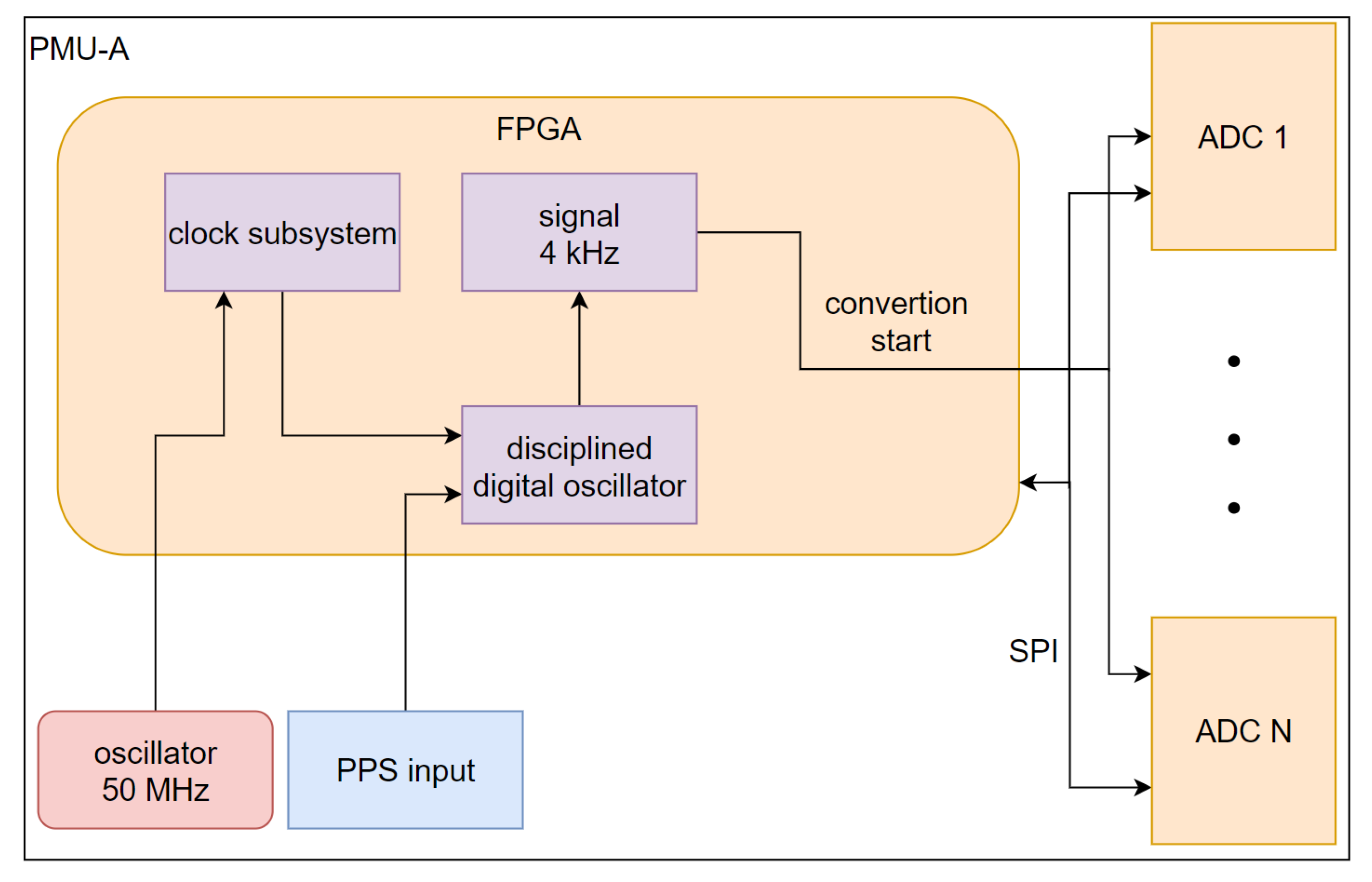
3.1. PMU-A

The architecture of the PMU-A (Figure 1) device was based on an FPGA circuit in order to achieve scalability of the solution. It is a modular device with multiple measurement cards that can be connected to the FPGA through independent SPIs (Serial Peripheral Interface). All measurement cards are equipped with ADCs (Analog to Digital Converters) driven by the same conversion start signal generated in the FPGA. Synchronization to UTC time is made with the use of PPS connected to FPGA and an internal dedicated disciplined digital oscillator module. This module generates a 4 kHz clock signal which is used to trigger the start of conversion in ADCs.
The general block diagram of the disciplined digital oscillator module is presented in Figure 2. The output 4 kHz signal is created from an internal 50 MHz clock using a 32-bit register. The register is incremented by the pre-calculated increment value. The counter counts 4-kHz signal periods between each PPS input rising edge, and the state of the 32-bit register value at the time of the PPS rising edge is used to calculate the error term summed with the increment value. To achieve stability of this feedback loop, the increment value is filtered through a low-pass filter.

3.2. PMU-B

The second hardware architecture (Figure 3) is a device developed for small cost-effective measurement devices such as PMU and MU with SV functionality; it is based on an STM32F765 microcontroller which carries out the synchronization procedure, reads and processes SV data from ADC, and provides communication through ethernet. As a clock source, it uses a TCVCXO, which is disciplined to the UTC time scale with the use of PPS signal.
The synchronization circuit is implemented entirely by microcontroller internal circuits (Figure 4). A 16.384 MHz TCVCXO oscillator provides a clock signal (CLK 1) which is connected to the external clock input of the microcontroller. The CLK 1 frequency is multiplied by 105/16 by the internal PLL (Phase Lock Loop) circuits of the microcontroller to obtain an internal clock (CLK 2) with a nominal frequency of 107.520 MHz. The CLK 2 clock is counted continuously by a 32-bit TIM2 timer working in input capture mode. The PPS signal applied to the external input of the microcontroller writes the TIM2 value to the internal latch of the microcontroller on its rising edge, which is then read by the microcontroller processing unit. The PPS pulse generates an interrupt (IRQ) that starts the next computational step of the synchronization algorithm. The output of the algorithm is a control voltage that tunes the TCVCXO oscillator through the use of a DAC (Digital to Analog Converter), ensuring that its frequency is disciplined to the UTC time scale. To obtain a 4 kHz sampling signal, CLK 2 is divided by the TIM3 counter working in PWM mode. The phase of the 4 kHz signal is aligned to the UTC time scale using the PPS signal.

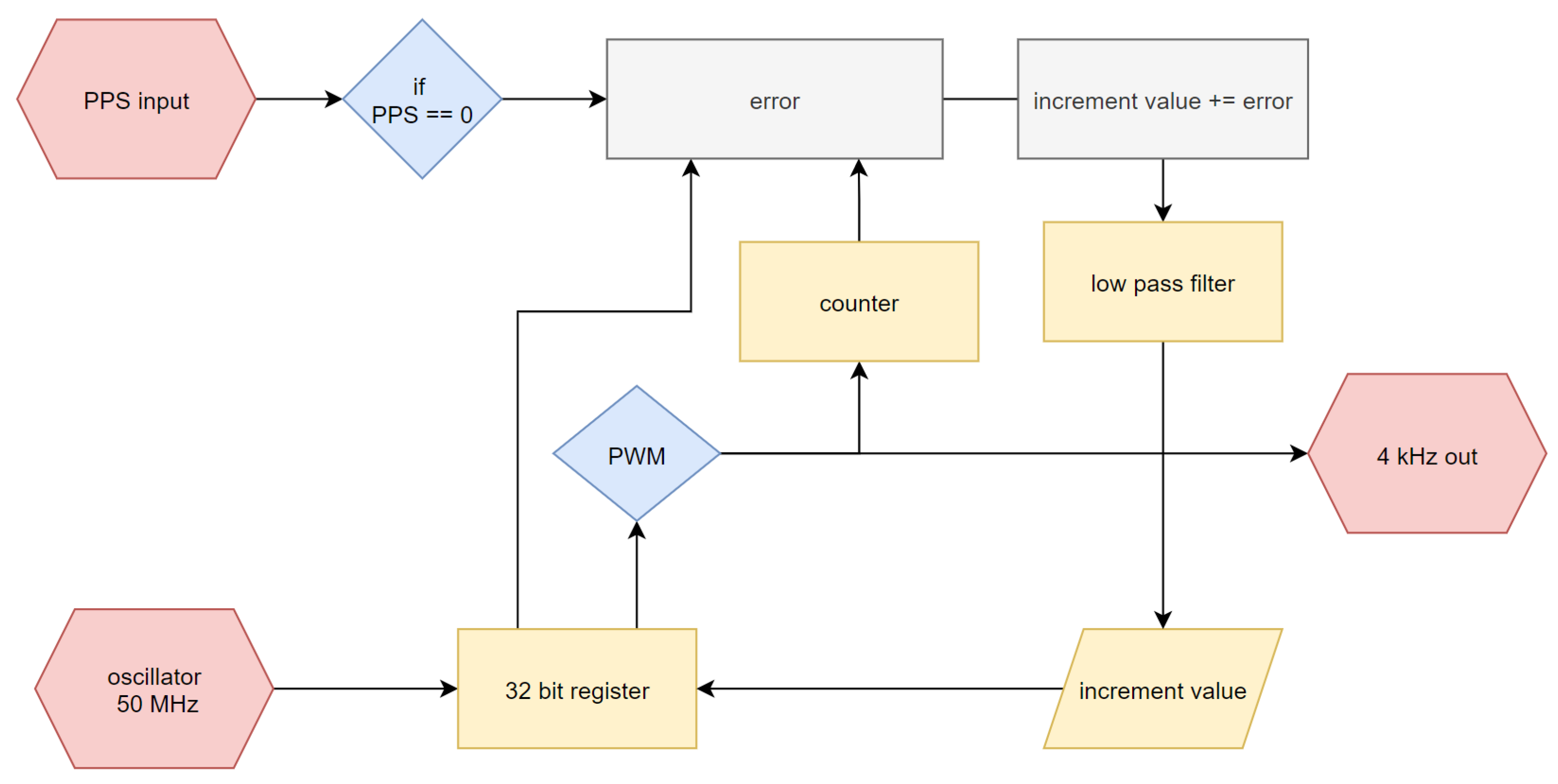
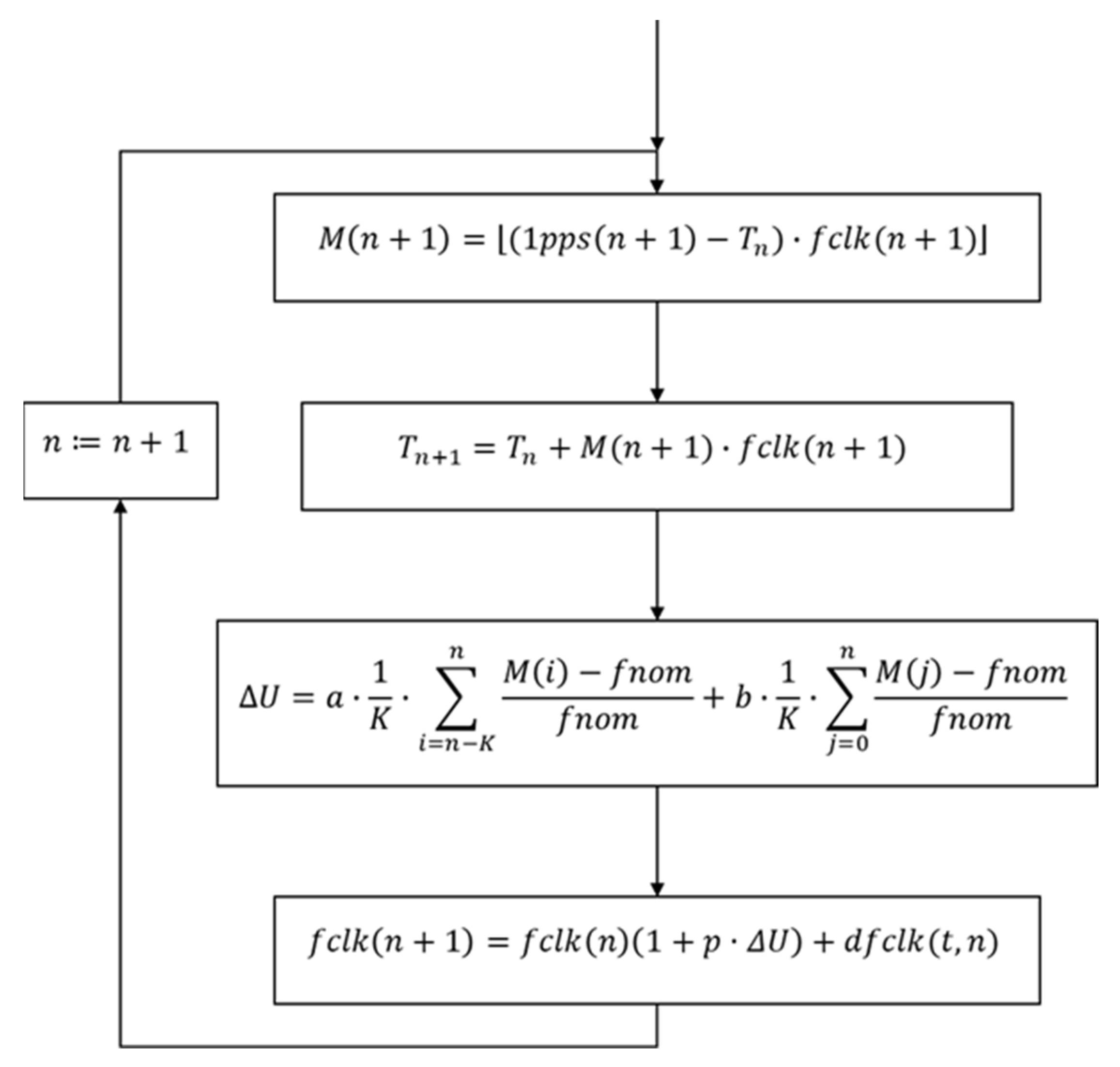
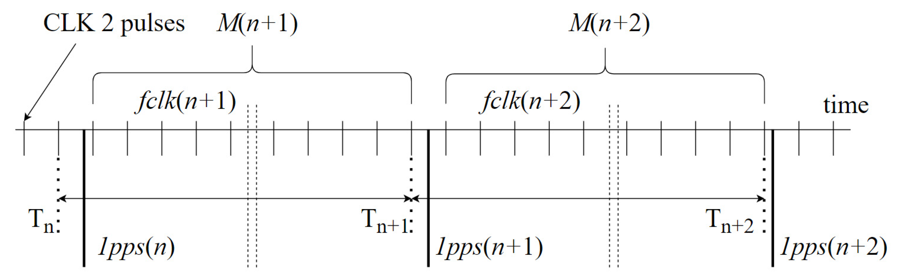
3.2.1. Synchronization Algorithm

The synchronization algorithm is presented in the following flow chart diagram (Figure 5) and refers to Figure 6, which models the actual counting process. The following symbols are used:
  • M(n) is the number of CLK 2 pulses counted by TIM2 between consecutive PPS pulses (└┘ denotes an integer part of a number);
  • fclk(n) is the frequency of CLK 2 signal between consecutive PPS pulses;
  • fnom is the nominal value of CLK 2 signal, equal to 107.520 MHz;
  • 1pps(n) is the arrival time of PPS pulse at n-epoch;
  • Tn is the moment in time of the last pulse of CLK 2 signal counted before the arrival of PPS pulse;
  • K is the frequency averaging time interval length (in seconds);
  • ΔU is the increment of TCVCXO tuning voltage computed at each pass of the loop of the synchronization algorithm;
  • a and b are the coefficients that ensure proper dynamical characteristics of the synchronization procedure;
  • dfclk(t,n) is a term expressing the TCVCXO frequency temperature and aging dependence.

3.2.2. Simulation

The correction voltage applied to the TCVCXO oscillator is based on the averaged deviation of the TCVCXO frequency from the nominal value 16.384 MHz and the accumulated phase error. To optimize the synchronization algorithm, and in particular to choose the optimal values for the a and b coefficients, a computational model of a counting circuit (Figure 6) that reflects the actual counting process as closely as possible was developed and simulated using Mathematica software. The accuracy of the counting model is important because it has to mirror a very important feature of the physical circuit, namely, that none of the CLK 2 signal pulses is lost or counted twice.
At the start of the simulation, the 1pps(1), …, 1pps(L) values, where L is the length of the simulation interval in seconds, was determined using a random variable with a uniform probability distribution.
During the simulation run, the TCOCXO frequency temperature dependence as well as the aging were taken into account using the dfclk(t,n) term. Based on the TCVCXO datasheet, the daily aging rate of the oscillator was assumed as 10−13. The temperature frequency fluctuations were assumed as 0.5 × 10⁻⁷ with, a fluctuation period equal to 2 h (values based on the datasheet of the TCVCXO oscillator).
All simulations started with the initial difference of the CLK 2 signal frequency from the nominal 107.52 MHz value equal to 10 ppm.
As can be seen from the flowchart, the synchronization algorithm uses the frequency deviation as well as the cumulative phase error to calculate the TCVCXO frequency correction voltage. The simulation results (Figure 7) show that the frequency accuracy in the synchronized state is better than 2 × 10⁻⁹. Disregarding the aging and temperature influence, such synchronization accuracy enables the maintenance of the 1 µs accuracy of the phase of 4 kHz signal relative to UTC for about ten minutes in hold-over mode.
The cumulative phase error term ensures that both the frequency and the phase of the TCVCXO oscillator follow the UTC time scale. Without this term, the phase runs off with an average speed of 240 ns/day, assuming aging equal to 10−13 per day. Moreover, the phase fluctuates with an amplitude of 2 µs due to the TCVCXO frequency variation with temperature (fluctuation amplitude 0.5 × 10⁻⁷ over 2-h period, simulating a 12-degree temperature change). Conversely, with the cumulative phase error term active, the simulation and the behavior of the real circuit both show that the TCVCXO phase remains within 200 ns of UTC time (Figure 8). UTC time scale phase tracking by TCVCXO signal is desirable because it makes the periodical resetting of the TCVCXO phase unnecessary.

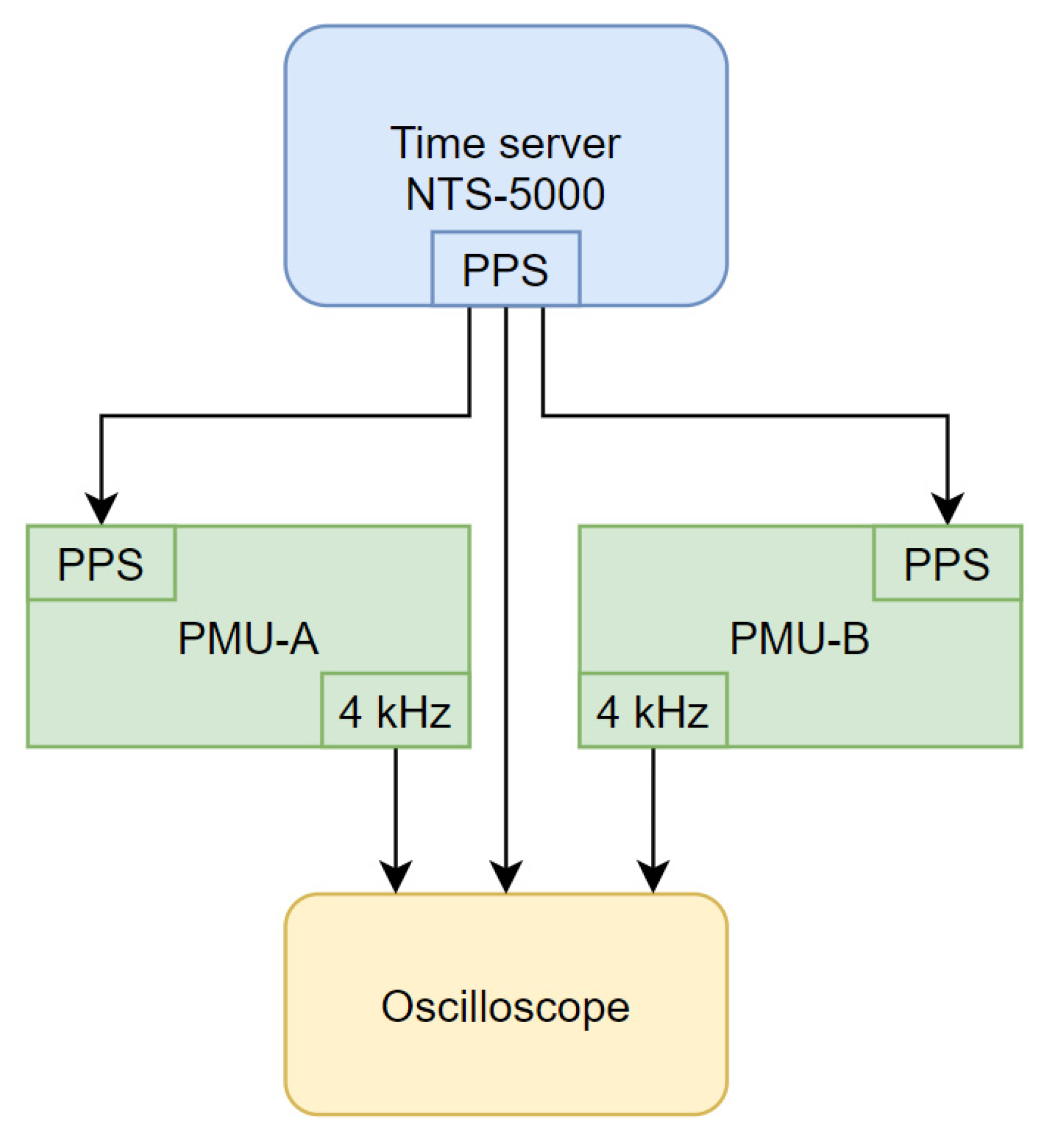
4. Experimental Setup

The synchronization precision of both devices was evaluated using the setup presented in Figure 9. An NTS-5000 time server with an internal OCXO oscillator with clock stability better than 1−10 per day was used as a reference PPS signal source. A DS4034 oscilloscope was used for time and frequency measurement. The PPS signal from the time server was connected to both PMUs and the oscilloscope.
The measurement procedure consisted of reading the time difference between the rising edge of the PPS signal and appropriate edges of the sampling signal. Over 10,000 such measurement results were obtained. All measurement data were sent to PC via ethernet, and SCPI (Standard Commands for Programmable Instruments) was used for further statistical analysis.

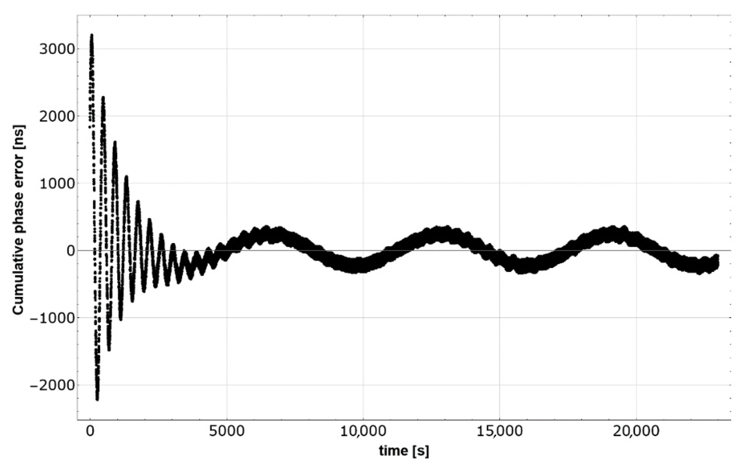
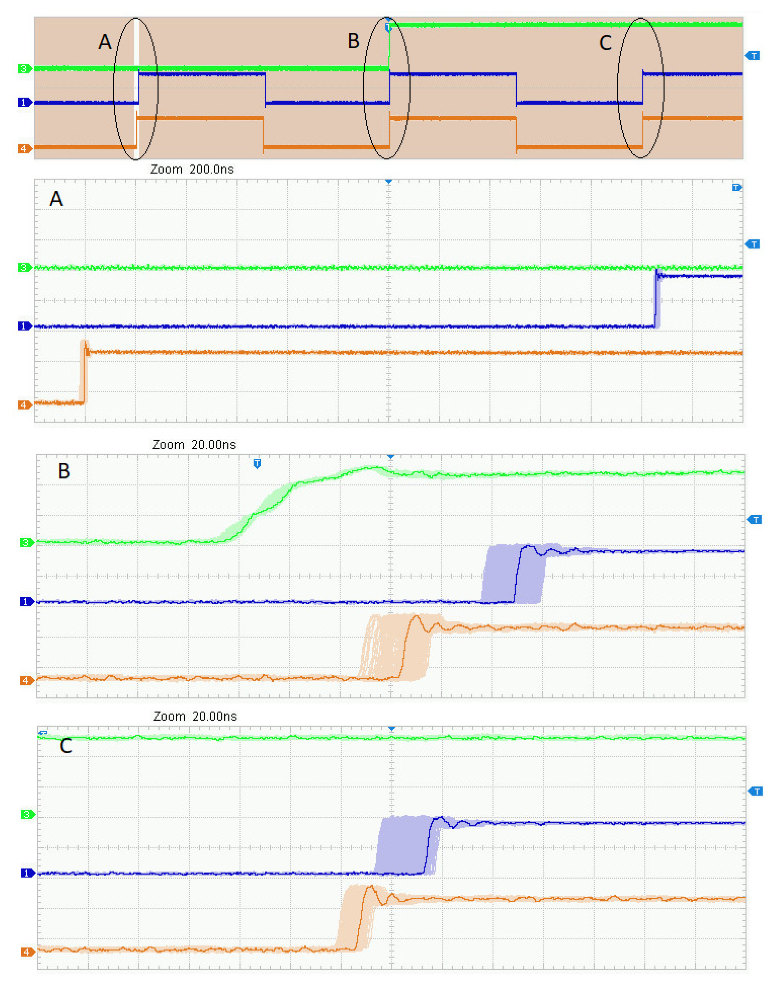
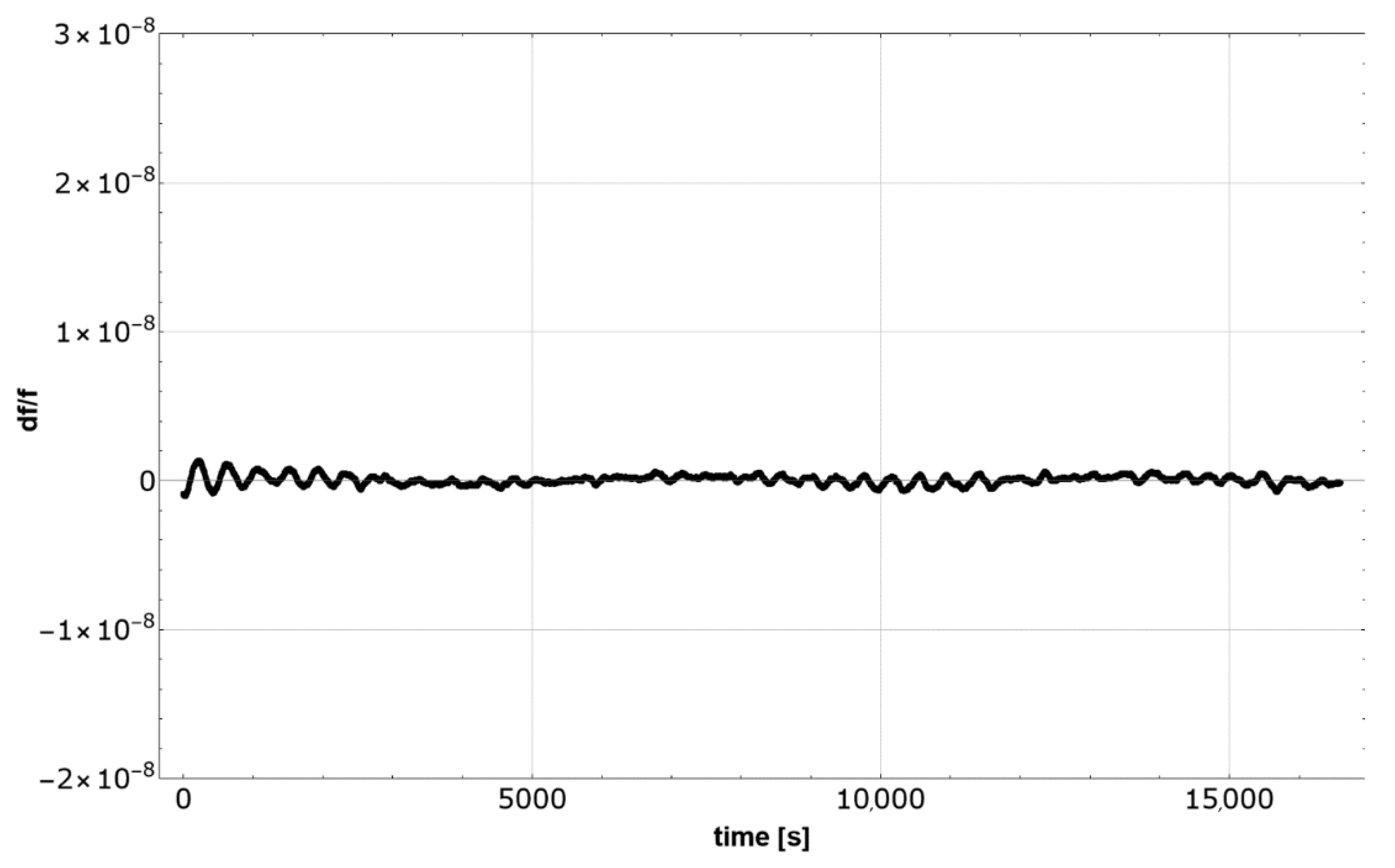
5. Results and Discussion

For the statistical analysis 10,000 samples of time differences between the sampling signal and reference signal were collected. Figure 10(A1) shows PMU-A and Figure 10(A2) shows PMU-B. The mean offset for PMU-A is equal to 79 nanoseconds, while for PMU-B it is equal to 49 nanoseconds. The standard deviation is equal accordingly, at 5.74 and 2.99 nanoseconds. These results show that PMU-B achieves better synchronization parameters than PMU-A in term of both offset from the reference signal and standard deviation. The advantage of the PMU-B circuit can be seen from the histograms of the time errors (Figure 10(B1,B2)). The histogram for PMU-A has a rectangular shape and that for PMU-B a Gaussian one, which means that the PMU-B output timing signal offset is more often near its mean value, which is a positive feature.
The above measurements show how precisely the sampling signals are synchronized to the PPS signal. However, it is important to measure and compare the signal frequency as well. To achieve this, the first period before and after the PPS signal was observed on an oscilloscope (Figure 11). The rising edges of sampling clocks from both devices were compared at three time instants. In the top part of Figure 11, the entire measurement window can be seen. Figure 11A presents the rising edges of the 4 kHz signal (PMU-A and PMU-B) before the PPS, Figure 11B the first rising edge of the 4 kHz signal after the PPS, and Figure 11C the second rising edge of the 4 kHz signal after the PPS.
The mean shifts in time between the sampling signals are accordingly 2290 ns, 40 ns, and 30 ns. Moreover, the duration between the rising edge of the PPS and the rising edges of the 4 kHz signal (PMU-A and PMU-B) before the PPS were measured as 247 µs and 250 µs, respectively.
These intervals mean that the frequency of 4 kHz signals have errors. This inaccuracy of the 4 kHz signal adds up periodically and creates a significant error at the end of a second. For PMU-A, this error is about 3 µs, while for PMU-B the error is too small to determine using this measurement technique.
The synchronization solution used in the PMU-A utilizes an internal crystal oscillator with a nominal frequency of 50 MHz for calculating the precise moment of the 4 kHz signal transition, however, the real internal oscillator frequency differs from the nominal value used in the firmware for calculations. Moreover, the real frequency can vary with the temperature because the crystal oscillator is not thermo-compensated. Using a high quality thermo-compensated crystal oscillator as a source for the 50 MHz clock could reduce the inaccuracy level, however, an offset would exist regardless if the oscillator frequency was not equal to exactly 50 MHz. The cause is a fractional part appearing when dividing Equation (1):
n = 0 P P S 1 f o s c / f p w m
where fosc is the crystal oscillator frequency (50 MHz), fpwm is the sampling signal frequency, and 0 P P S   is the number of fosc periods during one second of time.
There are at least two ways to increase the precision of the PMU-A without changing the inexpensive crystal oscillator. One is to increase the frequency of the internal clock in the FPGA with the use of a PLL internal circuit, and the second is to increase the length of the 32-bit register size (Figure 2). In both cases the gain in synchronization precision is linear, and as such it would be possible to decrease the synchronization error below 1 µs.
In the case of the PMU-B there are two factors that limit the synchronization precision, namely, the temperature dependence of the TCVCXO frequency (although the oscillator is thermally compensated) and the limited resolution of the DAC that produces the TCVCXO tuning voltage.

6. Conclusions

In this paper, two cost-effective circuits for sampling signal generation synchronized to a PPS signal have been presented. The first, PMU-A, is based on an FPGA device and a basic XO oscillator, and the second PMU-B is based on a microcontroller and TCVCXO oscillator. The novel control algorithm implemented in the PMU-B significantly improves the synchronization precision by introducing phase tracking of the synchronization signal by the local TCVCXO oscillator. Both circuits satisfy the requirements for PMU and MU devices used in power systems, though with restrictions in the case of PMU-A. IEC/IEEE 60255-118-1 requires time synchronization accuracy around 3.1 µs, while IEC 61850 requires it to be better than 4 µs for T4-class devices and 1 µs in the most restrictive T5 class. In the worst case, the PMU-A has a time synchronization accuracy of 2.29 µs, while for the PMU-B the accuracy is around 40 ns. This means that the architecture of the sampling system proposed in the PMU-B fits the requirements of both standards. The architecture of the sampling system proposed in the PMU-A fits only the requirements for synchrophasors and T4-class devices under IEC 61850.
In the case of PMU-A design, work can be carried out on the FPGA firmware to increase its synchronization precision, e.g., by increasing the resolution of calculations by extending the register size or by increasing the frequency of the internal clock. Both solutions target the problem of precision loss caused by the need to divide small integer values.
In the case of PMU-B, the synchronization precision is limited by the resolution of the internal DAC, and could be improved further by increasing the DAC resolution in the software via dithering methods. The synchronization accuracy of the output 4 kHz timing signal, especially its hold-over behavior, can be improved by using a higher stability local quartz oscillator.

Author Contributions

Conceptualization, K.M., A.L. and P.M.; methodology K.M. and A.L.; software K.M. and A.L.; validation A.L. and M.H.; formal analysis M.H.; investigation K.M. and A.L.; resources K.M., A.L. and P.M.; data curation K.M. and A.L.; writing—original draft preparation K.M., A.L. and P.M.; writing—review and editing A.L. and M.H.; visualization, K.M. and A.L.; supervision M.H.; project administration A.L.; funding acquisition P.M. and M.H. All authors have read and agreed to the published version of the manuscript.

Funding

This research received no external funding.

Data Availability Statement

Not applicable.

Conflicts of Interest

The authors declare no conflict of interest.

Abbreviations

ADCAnalog to Digital Converter
CPLDComplex Programmable Logic Device
CLK* clock
DACDigital to Analog Converter
FEFrequency Error
FIRFinite Impulse Response
FPGAField Programmable Gate Array
FRErate of change of FRequency Error
GPSGlobal Positioning System
GNSSGlobal Navigation Satellite Systems
IECInternational Electrotechnical Commission
IEDIntelligent Electronic Devices
IEEEInstitute of Electrical and Electronics Engineers
MUMerging Unit
nsnanosecond
OCXOOven Controlled Crystal Oscillator
PPSPulse Per Second
PLLPhase Lock Loop
PTPPrecision Time Protocol
PWMPulse Width Modulation
PMUPhasor Measurement Units
RESRenewable Energy Sources
RMSRoot Mean Square
ROCOFRate Of Change Of Frequency
SPISerial Peripheral Interface
SVSampled Values
SCPIStandard Commands for Programmable Instruments
TIETime Interval Error
TIMtimer
TVETotal Vector Error
TCVCXOTemperature Compensated Voltage Controlled Crystal Oscillator
UTCCoordinated Universal Time

References

  1. Lagos, D.; Papaspiliotopoulos, V.; Korres, G.; Hatziargyriou, N. Microgrid Protection Against Internal Faults: Challenges in Islanded and Interconnected Operation. IEEE Power Energy Mag. 2021, 19, 20–35. [Google Scholar] [CrossRef]
  2. Jones, K.W.; Pourbeik, P.; Kobet, G.; Berner, A.; Fischer, N.; Huang, F.; Holbach, J.; Jensen, M.; O’Connor, J.; Patel, M. Impact of inverter based generation on bulk power system dynamics and short-circuit performance. In Task Force on Short-Circuit and System Performance Impact of Inverter Based Generation; Tech. Rep. PES-TR68; IEEE: Piscataway, NJ, USA, 2018. [Google Scholar]
  3. IEC/IEEE 60255-118-1-2018; Measuring Relays and Protection Equipment–Part 118-1: Synchro-Phasor for Power Systems–Measurements. IEEE: Piscataway, NJ, USA, 2018.
  4. Pavičić, I.; Holjevac, N.; Ivanković, I.; Brnobić, D. Model for 400 kV Transmission Line Power Loss As-sessment Using the PMU Measurements. Energies 2021, 14, 5562. [Google Scholar] [CrossRef]
  5. Xiaotao, C.; Hangli, J.; Qian, S.; Dong, S.; Wujun, H.; Shihui, Y.; Weimin, L.; Yalin, L.; De, S.; Jiang, L. Fault Location Technology of Transmission Line based on Asynchronous Phasor Measurement from PMUs. IOP Conf. Ser. Earth Environ. Sci. 2021, 645, 012084. [Google Scholar] [CrossRef]
  6. Rong, C.; Cao, C.; Jian, H.; Li, J.; Chen, J. Fault Location Technology of Transmission Line and Asynchronous Phasor Measurement from PMUs. In Proceedings of the 2020 IEEE 4th Conference on Energy Internet and Energy System Integration (EI2), Wuhan, China, 30 October–1 November 2020; pp. 292–297. [Google Scholar]
  7. Paramo, G.; Bretas, A.; Meyn, S. Research Trends and Applications of PMUs. Energies 2022, 15, 5329. [Google Scholar] [CrossRef]
  8. Rebello, E.; Vanfretti, L.; Almas, M.S. Experimental testing of a real-time implementation of a PMU-based wide-area damping control system. IEEE Access 2020, 8, 25800–25810. [Google Scholar] [CrossRef]
  9. Borghetti, A.; Bottura, R.; Barbiroli, M.; Nucci, C.A. Synchrophasors-based distributed secondary voltage/VAR control via cellular network. IEEE Trans. Smart Grid 2016, 8, 262–274. [Google Scholar] [CrossRef]
  10. Stastny, L.; Franek, L.; Bradac, Z. Time synchronized low-voltage measurements for smart grids. Procedia Eng. 2015, 100, 1389–1395. [Google Scholar] [CrossRef]
  11. Del Prete, S.; Delle Femine, A.; Gallo, D.; Landi, C.; Luiso, M. Implementation of a distributed stand alone merging unit. J. Phys. Conf. Ser. 2018, 1065, 052042. [Google Scholar] [CrossRef]
  12. Ozansoy, C.R.; Zayegh, A.; Kalam, A. Time synchronisation in a IEC 61850 based substation automation system. In Proceedings of the 2008 Australasian Universities Power Engineering Conference, Sydney, Australia, 14–17 December 2008; pp. 1–7. [Google Scholar]
  13. IEC 61850-5:2013; Communication requirements for functions and device models. International Electrotechnical Commission: Geneva, Switzerland, 2013. Available online: https://webstore.iec.ch/publication/6012 (accessed on 12 September 2022).
  14. Liu, Z.; Chen, X.; Liu, J.; Li, C. High precision clock bias prediction model in clock synchronization system. Math. Probl. Eng. 2016, 2016, 1813403. [Google Scholar] [CrossRef]
  15. Shmaliy, Y.S.; Ibarra-Manzano, O. Clock current state estimation with a Kalman-like algorithm employing measurement of time errors. In Proceedings of the 2011 Joint Conference of the IEEE International Frequency Control and the European Frequency and Time Forum (FCS) Proceedings, San Francisco, CA, USA, 1–5 May 2011; pp. 1–4. [Google Scholar] [CrossRef]
  16. Arceo-Miquel, L.; Shmaliy, Y.S.; Ibarra-Manzano, O. Optimal synchronization of local clocks by GPS 1PPS signals using predictive FIR filters. IEEE Trans. Instrum. Meas. 2009, 58, 1833–1840. [Google Scholar] [CrossRef]
  17. Bui, T.Q.T.; Elango, A.; Landry, R.J. FPGA-Based Autonomous GPS-Disciplined Oscillators for Wireless Sensor Network Nodes. Sensors 2022, 22, 3135. [Google Scholar] [CrossRef] [PubMed]
  18. Boehmer, T.J.; Bilén, S.G. Low-Power GPS-Disciplined Oscillator Module for Distributed Wireless Sensor Nodes. Electronics 2021, 10, 716. [Google Scholar] [CrossRef]
  19. Pawłowski, E.; Warda, P. Method and system for disciplining a local reference oscillator by GPS 1PPS signal. Przegląd Elektrotechniczny 2018, 7, 94. [Google Scholar] [CrossRef]
  20. Yao, W.; Zhan, L.; Liu, Y.; Till, M.J.; Zhao, J.; Wu, L.; Teng, Z.; Liu, Y. A novel method for phasor measurement unit sampling time error compensation. IEEE Trans. Smart Grid 2016, 9, 1063–1072. [Google Scholar] [CrossRef]
  21. Connor-Winfield’s FTS250-HP GPS Disciplined Oscillator. Available online: http://www.conwin.com/datasheets/sg/sg176.pdf (accessed on 12 September 2022).
Figure 1. Block scheme of sampling signal generation in PMU-A.
Energies 15 07095 g001
Figure 2. PPS-disciplined digital oscillator implemented in FPGA.
Energies 15 07095 g002
Figure 3. Block scheme of sampling signal generation in PMU-B.
Energies 15 07095 g003
Figure 4. Sampling signal generation implementation in STM32F765 microcontroller.
Energies 15 07095 g004
Figure 5. Clock synchronization algorithm.
Energies 15 07095 g005
Figure 6. Time diagram of the counting process.
Energies 15 07095 g006
Figure 7. The simulation results of frequency accuracy in synchronized state, PMU-B.
Energies 15 07095 g007
Figure 8. Cumulative phase error in behavior, PMU-B.
Energies 15 07095 g008
Figure 9. Experimental setup for sampling signal quality measurements.
Energies 15 07095 g009
Figure 10. Sampling signal measurement data statistical analysis. A1—sampling signal delay from PPS for PMU-A, B1—histogram of sampling signal delay for PMU-A, C1—box plot of sampling signal delay for PMU-A. A2,B2,C2—accordingly for PMU-B.
Energies 15 07095 g010
Figure 11. Rising edge comparison of sampling clock around PPS signal. A—sampling edge before PPS, B—first sampling edge after PPS, C—second sampling edge after PPS. Channel 4 (orange)—PMU-B, channel 1 (blue)—PMU-A, channel 3 (green)—PPS.
Energies 15 07095 g011
Table 1. IEC 61850 time synchronization class requirements.
IEC Time Synchronization ClassTime Synchronization Accuracy Requirements
T1±1 ms
T2±0.1 ms
T3±25 μs
T4±4 μs
T5±1 μs
Publisher’s Note: MDPI stays neutral with regard to jurisdictional claims in published maps and institutional affiliations.

