Article

High Performance 3.3 kV SiC MOSFET Structure with Built-In MOS-Channel Diode

Department of Electronic Engineering, Sogang University, Seoul 04107, Korea
*
Author to whom correspondence should be addressed.
Energies 2022, 15(19), 6960; https://doi.org/10.3390/en15196960
Submission received: 29 August 2022 / Revised: 16 September 2022 / Accepted: 20 September 2022 / Published: 22 September 2022
(This article belongs to the Special Issue Analysis of SiC MOSFETs for Advanced Energy-Conversion Systems)

Abstract

:
Built-in freewheeling diode metal–oxide–semiconductor field-effect transistors (MOSFETs) that ensure high performance and reliability at high voltages are crucial for chip integration. In this study, a 4H–SiC built-in MOS-channel diode MOSFET with a center P+ implanted structure (CIMCD–MOSFET) is proposed and simulated via technology computer-aided design (TCAD). The CIMCD–MOSFET contains a P+ center implant region, which protects the gate oxide edge from high electric field crowding. Moreover, the region also makes it possible to increase the junction FET (JFET) and N-drift doping concentration of the device by dispersing the high electric field. Consequently, the CIMCD–MOSFET is stable even at a high voltage of 3.3 kV without static degradation and gate oxide reliability issues. The CIMCD–MOSFET also has higher short-circuit withstanding capability owing to the low saturation current and improved switching characteristics due to the low gate-drain capacitance, compared to the conventional MOSFET (C–DMOSFET) and the built-in Schottky barrier diode MOSFET (SBD–MOSFET). The total switching time of a CIMCD–MOSFET is reduced by 52.2% and 42.2%, and the total switching loss is reduced by 67.8% and 41.8%, respectively, compared to the C–DMOSFET and SBD–MOSFET.

1. Introduction

Silicon carbide (SiC) is receiving considerable attention as an alternative to silicon for use in next-generation power semiconductors owing to its high thermal conductivity and breakdown voltage resulting from its wide bandgap [1,2,3]. SiC metal–oxide–semiconductor field-effect transistors (MOSFETs) enable faster switching operations than Si insulated-gate bipolar transistors (IGBTs) [4]. Therefore, several power modules using SiC MOSFET devices that can withstand voltages in the range of 650 V to 1.7 kV have been proposed [5,6,7]. Research on SiC MOSFETs for applications with a high voltage of 3.3 kV and higher is also being actively pursued [8,9].
SiC Schottky barrier diodes (SBDs) are the most widely used external anti-parallel diodes in power module systems. An SBD has a low diode turn-on voltage, which can reduce the dead time loss; moreover, its unipolar device operation significantly reduces the reverse recovery charge [10,11,12]. In addition, the switching loss is small even at high temperatures because the reverse recovery charge of the SiC SBD does not depend on temperature [13,14]. However, an additional external SBD requires a large assembly area, which increases the size of the power module system [15]. In addition, an increase in the operating voltage increases the size of the SBD, thus requiring a larger active area [16]. The built-in PiN body diode can be used to reduce the size of the power-module system. However, the high turn-on voltage and bipolar degradation cause conduction loss. Additionally, the high reverse recovery charge and temperature-dependent bipolar operation cause a large switching loss in high-temperature and high-speed switching operations [17,18].
Several methods for embedding a unipolar diode in a MOSFET have been developed to address these limitations. The best-known approach is to embed an SBD within a MOSFET [19,20,21,22,23]. Through this approach, the size of the power module system was reduced using the built-in SBD MOSFET while reducing the energy loss through a low turn-on voltage and small reverse recovery charge. However, barrier lowering occurs in the Schottky junction owing to image force, and additionally, the thermionic emission and tunneling process at the lower energy barrier increases the off-state leakage current at high voltage and high temperature conditions of the built-in SBD MOSFETs [24,25,26].
Embedded polySi/SiC heterojunction diode MOSFETs (HJD–MOSFETs) are designed to reduce the reverse recovery charge of the body diode [27,28,29]. The HJD–MOSFET operates as a unipolar body diode and the reverse recovery charge can be reduced to a level that is similar to that of the SBD. However, it is not suitable for use at high voltages because of the low critical electric field of polysilicon and the large off-state leakage current due to the interfacial trap charge at the polySi/SiC interface [30,31].
A built-in MOS-channel diode MOSFETs (MCD–MOSFETs) have also been proposed to reduce the diode turn-on voltage and reverse recovery charge of the body diode [32,33,34]. However, because only one channel is formed in the on state of the MCD–MOSFET, the static characteristics deteriorate, and the low P-base doping concentration causes a reach-through problem at high voltages [35]. In addition, the split gate structure and thin gate oxide film create a large electric field at the oxide edge due to electric field crowding and impair the reliability of the gate oxide film [32,36]. This reduces the stability of the MCD–MOSFET at high voltages.
In this study, a 3.3 kV center-implanted embedded MOS-channel diode MOSFET (CIMCD–MOSFET) was proposed and analyzed via technology computer-aided design (TCAD) simulations. The proposed structure has P+ doping in the center region, which distributes the electric field and reduces electric field crowding at the oxide edge of the MCD–MOSFET. Therefore, the CIMCD–MOSFET operation is stable even at a high voltage of 3.3 kV without the reliability issues resulting from the oxide film. Moreover, the diode turn-on voltage can be further reduced by reducing the oxide thickness of the MOS-channel diode. In addition, the doping concentration of the junction FET (JFET) and drift region can be increased owing to the shielding effect of the central P+ doping region, thereby minimizing the degradation of static characteristics. The simulation results demonstrate that the CIMCD–MOSFET has improved static characteristics, switching characteristics, and short-circuit capability compared with conventional diffusion MOSFETs (C–DMOSFET) and built-in Schottky barrier diode MOSFETs (SBD–MOSFET).

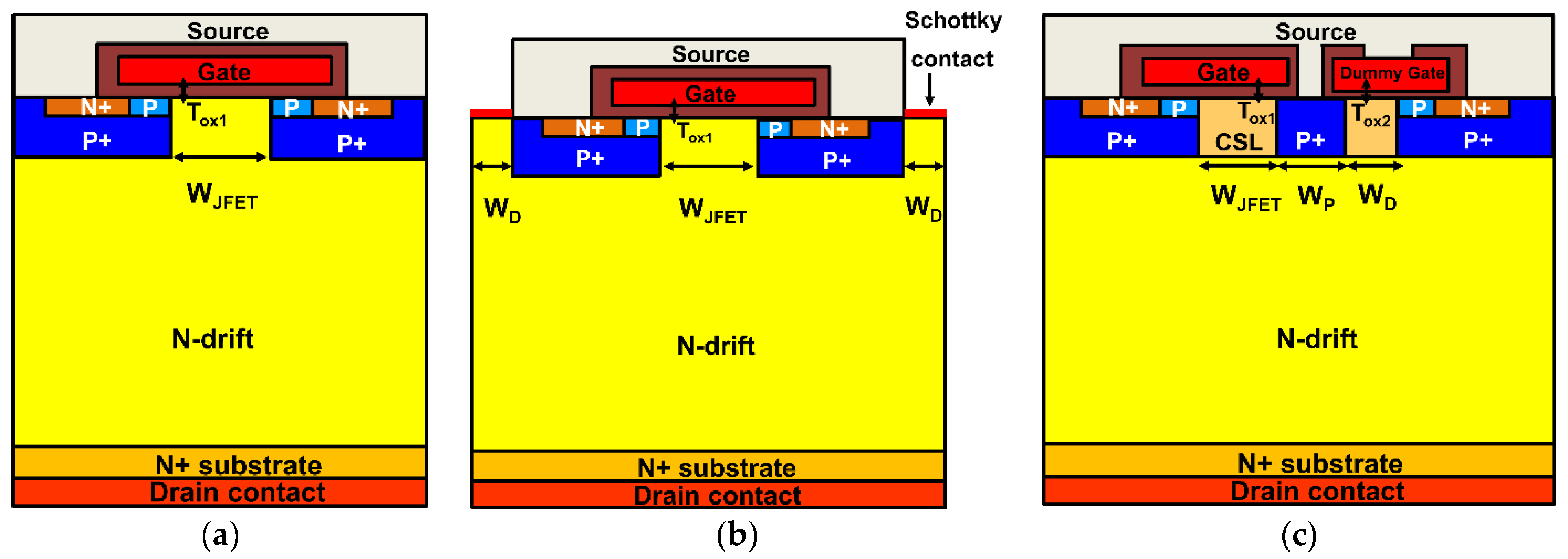
2. Device Optimizations and Methods

Figure 1 shows the cross-sectional views of the C–DMOSFET, SBD–MOSFET, and CIMCD–MOSFET. To prevent the reach-through problem, P+ doping was applied to the P-base region of the MCD–MOSFET, except for the channel region [37]. As shown in Figure 1b, it is possible to use the built-in Schottky barrier diode through the Schottky contact in the mesa region of the SBD–MOSFET, compared to the C–DMOSFET. The work function of the SBD–MOSFET was set to 4.33 eV, which is the same as that of titanium [38,39].
As shown in Figure 1c, the CIMCD–MOSFET has a split-gate structure. The right-side split dummy gate is in contact with the source while the left-side split gate is in contact with the gate. When the MOSFET is turned on, a channel is formed in the left P-base and current flows. When the MOSFET is turned off and the diode is turned on, a channel is formed in the right P-base due to the voltage difference between the source and drain and current flows. To reduce the turn-on voltage of the MOS-channel diode, the thickness of Tox2 should be 5 nm, which is much smaller than that of Tox1.
A shielding region was also formed by the P+ doping in the center region of the MCD–MOSFET structure, as shown in Figure 1c. The central P+ shielding region overlaps with the oxide edge below the split gate to directly protect the oxide from the high electric field and prevent field crowding at the oxide edge. In addition, the center-implanted P+ region improves the breakdown capability of the MOSFET by dispersing the high electric field in the P+ base region, thereby increasing the doping concentration of the JFET and N-drift region. Table 1 summarizes the parameters of the device structure. Figure 2a shows Baliga’s figure of merit (B–FOM) of the CIMCD–MOSFET according to the N-drift doping concentration (ND) and JFET width (WJFET). The B–FOM is defined as the square of the breakdown voltage (BV) divided by the specific on-resistance (Ron-sp) [40]. The WJFET and ND are important parameters that affect the Ron-sp and BV. The longer the WJFET, the lower the JFET resistance. However, the BV decreases and the cell pitch increases. This decreases the device integration in the active area. Also, the doping concentration of the N-drift increases, and the Ron-sp and BV decrease. As shown in Figure 2a, the CIMCD–MOFSET has the highest B–FOM value when WJFET = 1.8 μm and the doping concentration of N-drift is 3.5 × 1015 cm−3. Figure 2b shows the body diode turn-on voltage VF that is based on the width of the WD. A longer WD improves the diode current flow, decreases the VF, and decreases the cell density because the cell pitch increases. As the VF does not change significantly for a WD length of 1 μm or more, it is reasonable to maintain the WD length at 1 μm.
The simulation results of each device were obtained using the Sentaurus TCAD simulation package. The electron/hole continuity equations and Poisson equations were solved by considering mobility degradation and recombination in the simulation. The Lombardi interface charge model and high-field saturation were applied to the mobility model [41]. The Shockley–Read–Hall recombination and Auger recombination models were considered and the Hatakeyama model was applied [42]. In addition, we applied an incomplete ionization model, anisotropic mobility, and bandgap narrowing. Barrier lowering, barrier tunneling, and thermionic emission were considered for the Schottky contacts [43]. Furthermore, the channel mobility was estimated to be 15–20 cm2/V·s through the SiC/SiO2 interface charge and a thermodynamic model was considered for a high-temperature simulation [44,45].

3. Simulation Results and Analysis

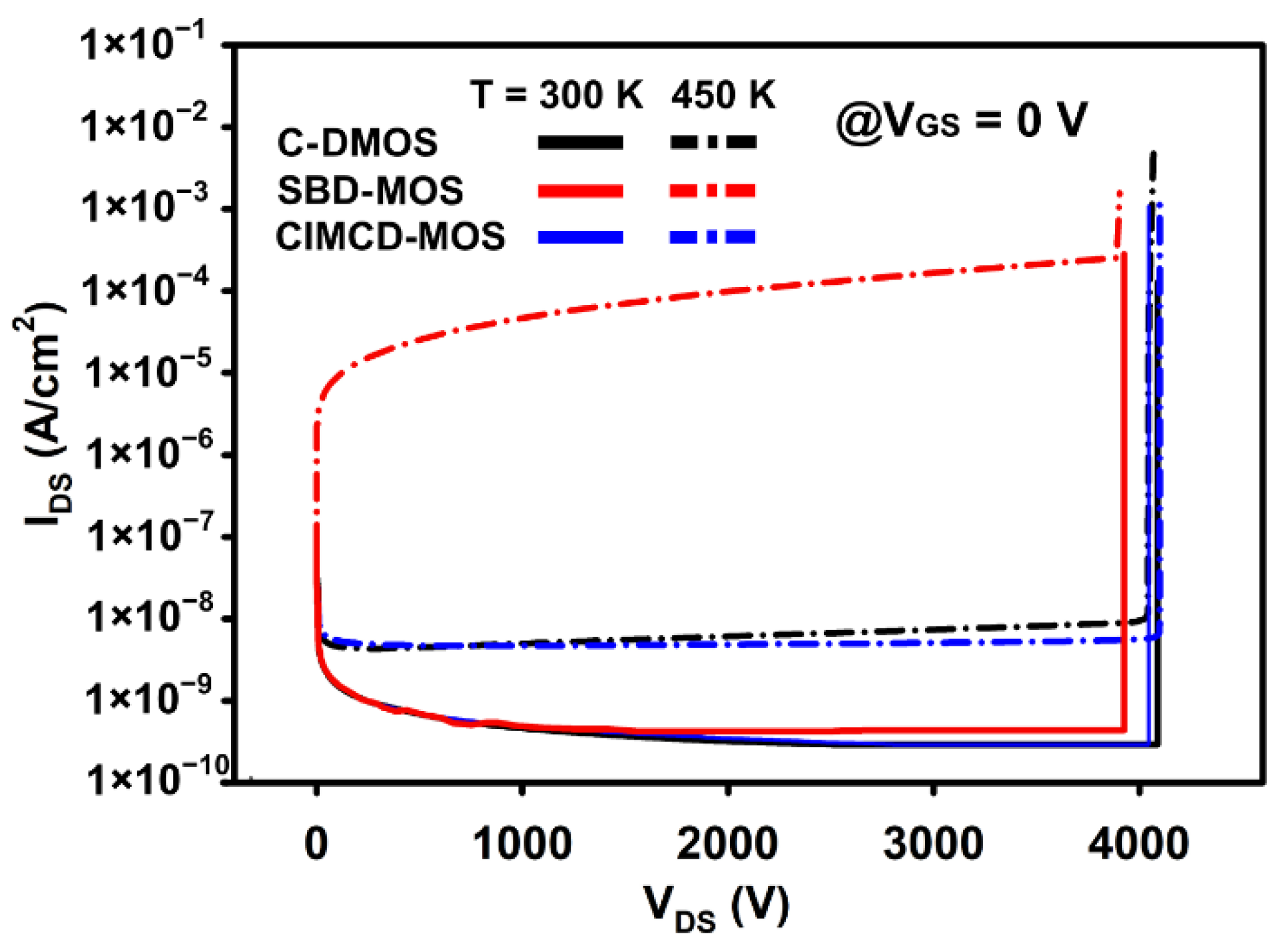
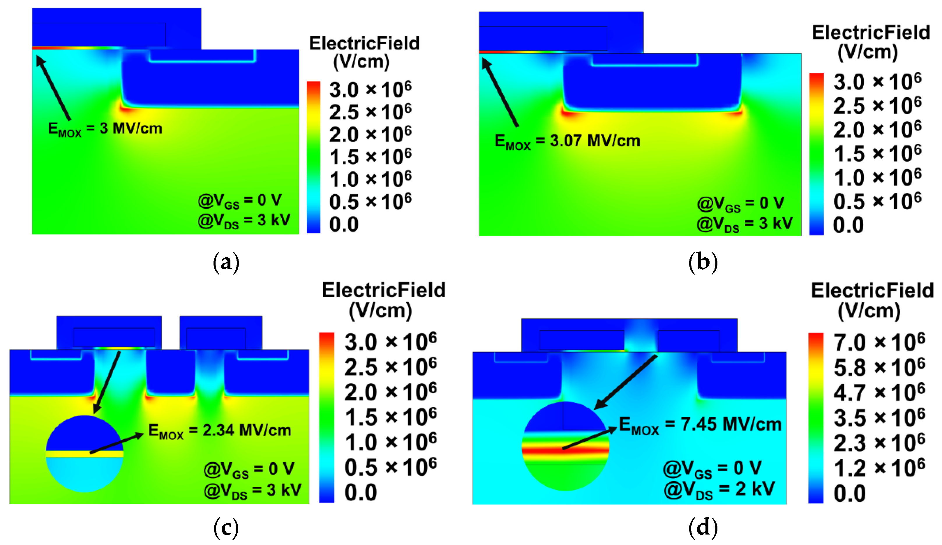
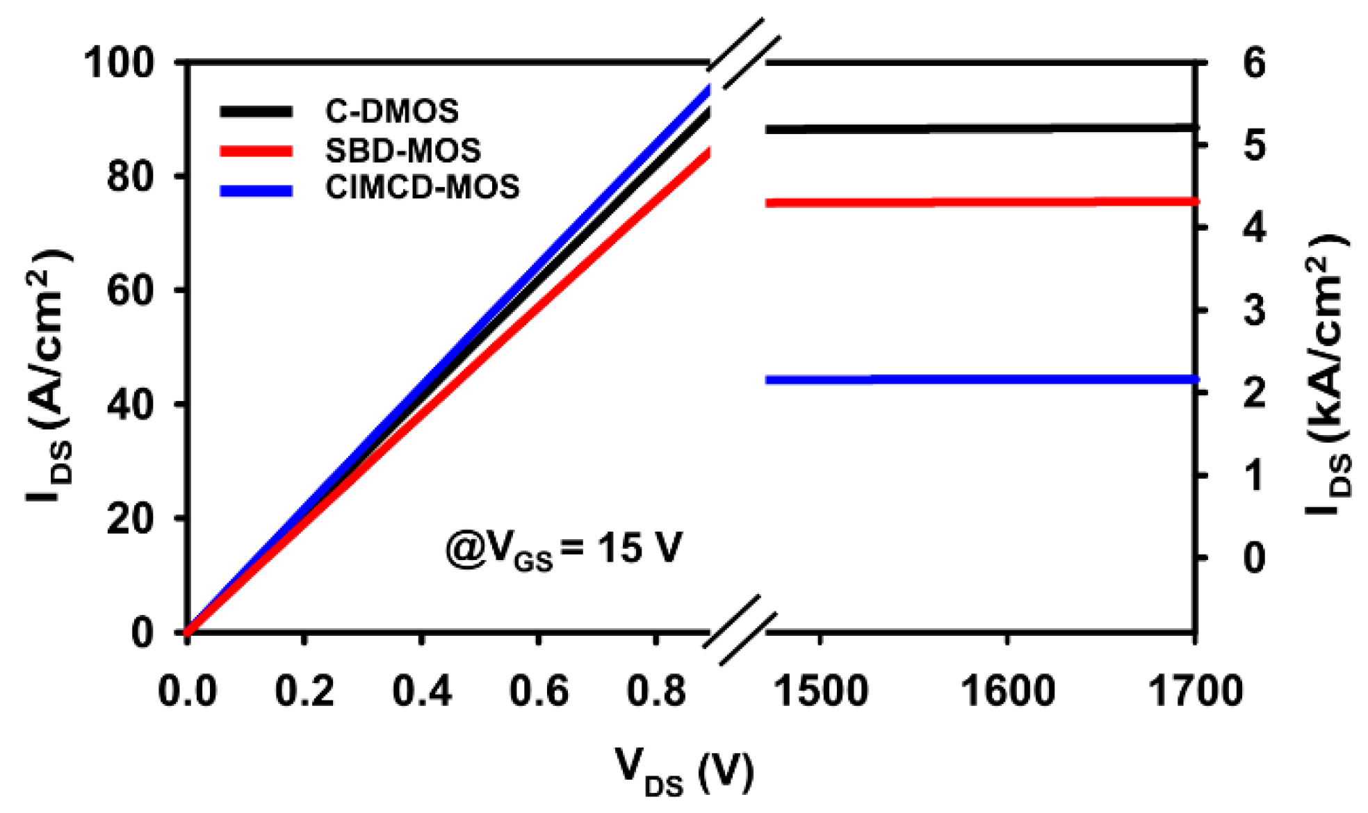
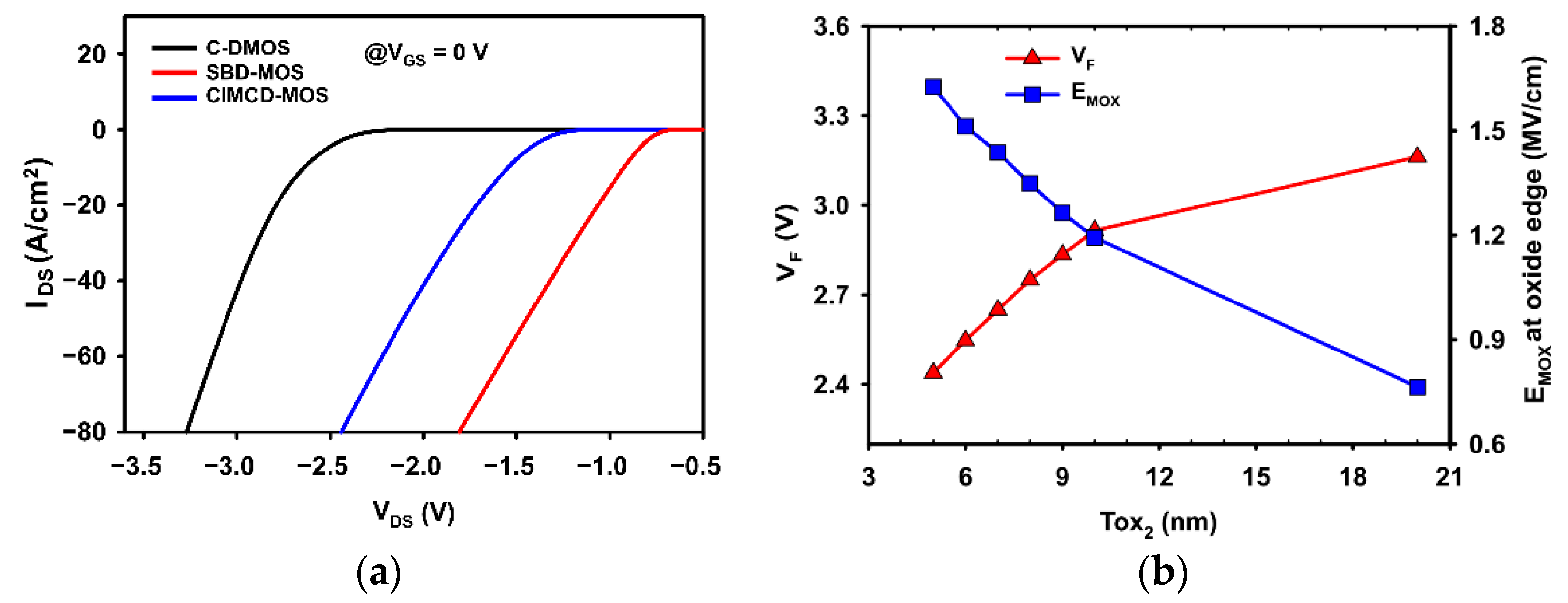
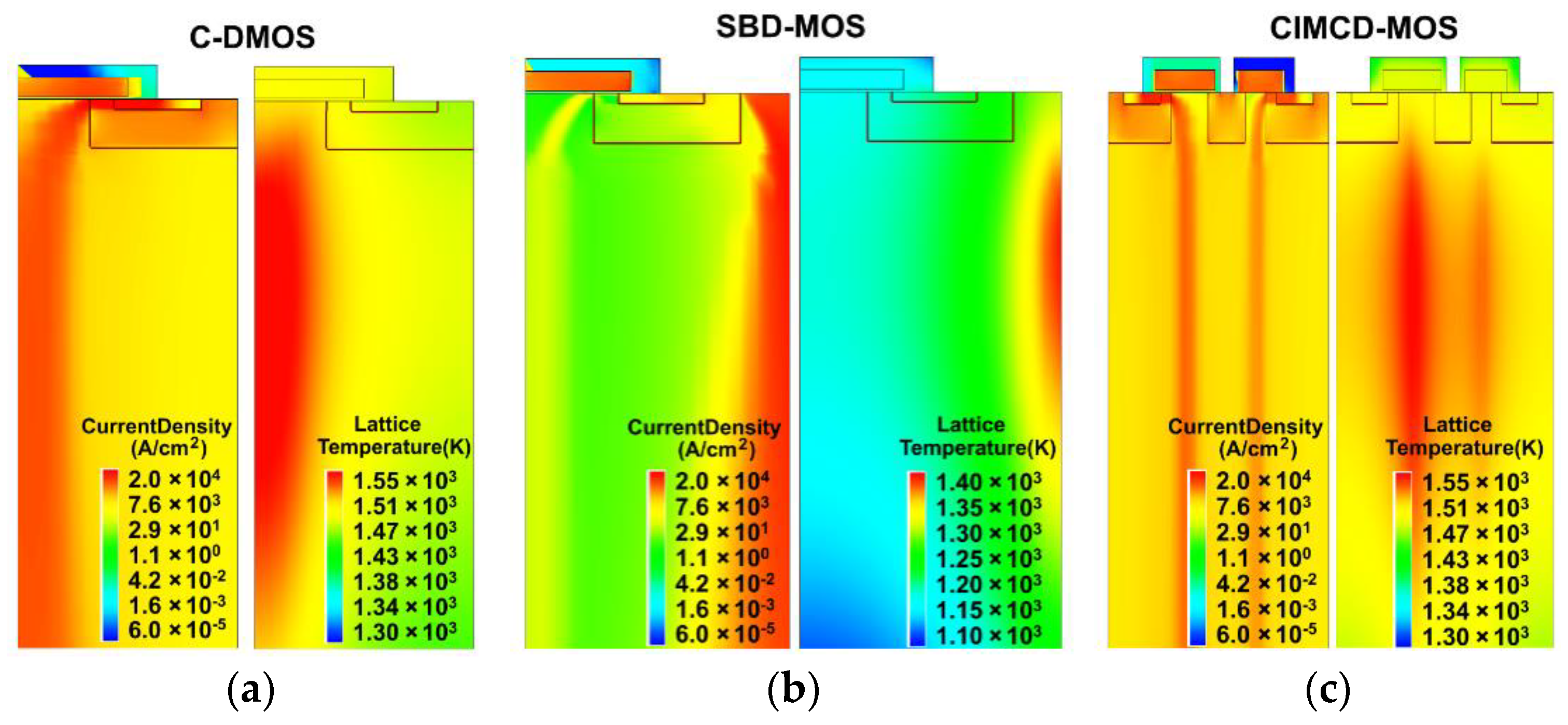
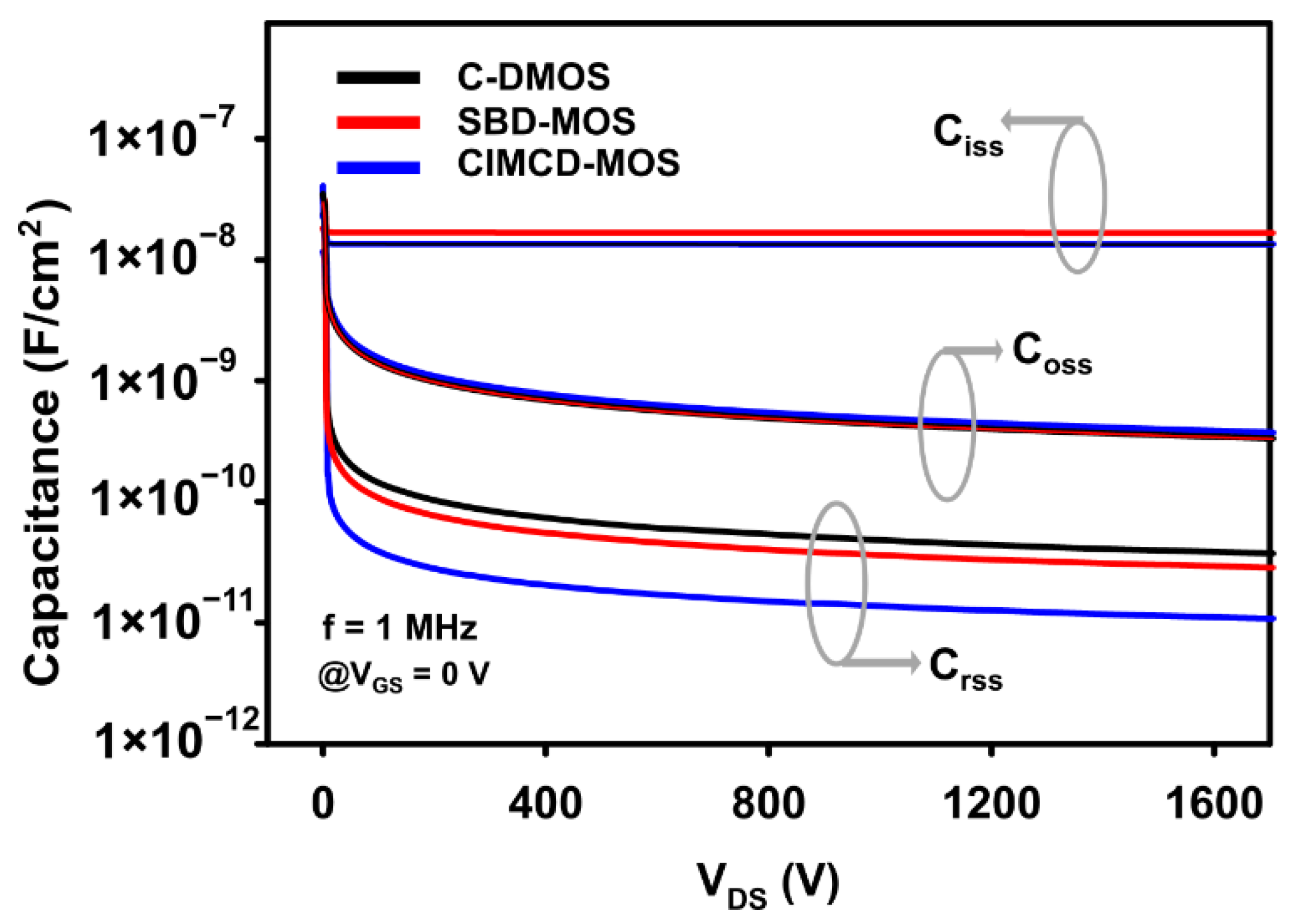
3.1. Static Performances

Figure 3 shows the off-state characteristics of the C–DMOSFET, SBD–MOSFET, and CIMCD–MOSFET. They have a breakdown voltage of over 3.3 kV at T = 300 K. At T = 450 K, additionally, the off-state leakage current is high in the SBD–MOSFET compared to the C–DMOSFET and CIMCD–MOSFET. Due to the tunneling effect of electrons in a thermally excited metal, called thermionic-field emission, the reverse leakage current of SBD–MOSFET is highly temperature-dependent [46]. Figure 4 shows the electric field distribution of each device. For improved reliability of the gate oxide film, the maximum electric field EMOX of the gate oxide is preferably ≤3 MV/cm [47]. In Figure 4a,b, the EMOX of the C–DMOSFET and SBD–MOSFET is approximately 3 MV/cm at VDS = 3 kV. The MCD–MOSFET without the center implant region applies a large electric field of 7.45 MV/cm to the oxide edge, even at VDS = 2 kV (Figure 4d). A large electric field across the thin gate oxide causes a large off-state leakage current due to tunneling and causes premature breakdown at low voltages. Conversely in Figure 4c, the center implant region of the CIMCD–MOSFET overlaps with the oxide edge to block the electric field. Moreover, by dispersing the electric field, a lower electric field is applied to the oxide film compared to the C–DMOSFET and SBD–MOSFET, even at a high voltage of VDS = 3 kV.
Figure 5 shows the on-state characteristics of each device. The CIMCD–MOSFET uses only a single channel in the on state, resulting in static degradation. Its saturation current is also smaller compared to the C–DMOSFET and SBD–MOSFET. However, owing to the increase in the breakdown voltage capability of the center implant region, the doping concentration of the JFET and N-drift can be increased and the static degradation can be minimized. As a result, the CIMCD–MOSFET has the highest B–FOM compared to the C–DMOSFET and SBD–MOSFET, despite being a single-channel MOSFET.
Figure 6a shows the third quadrant characteristics of the C–DMOSFET, SBD–MOSFET, and CIMCD–MOSFET. Owing to the Schottky barrier, the SBD–MOSFET has the lowest VF. The VF of the CIMCD–MOSFET is proportional to Tox2. In Figure 6b, the VF decreases as Tox2 decreases, but the electric field crowding at the oxide edge increases. Owing to the center implant shielding region, reducing the thickness of Tox2 to 5 nm does not cause oxide film reliability issues, resulting in a lower VF than the C–DMOSFET’s PiN body diode. Table 2 summarizes the static characteristics of the C–DMOSFET, SBD–MOSFET, and CIMCD–MOSFET. The CIMCD–MOSFET shows the highest oxide reliability characteristics among the three devices owing to the center implant area. The B–FOM is improved by 2.05% and 11.17% compared to the CMOSFET and SBD–MOSFET, respectively, by minimizing static degradation.

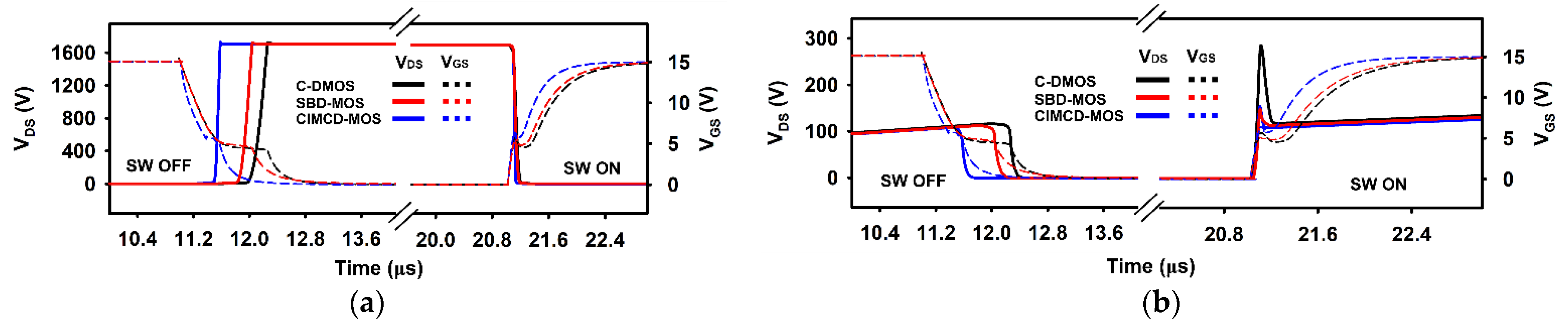
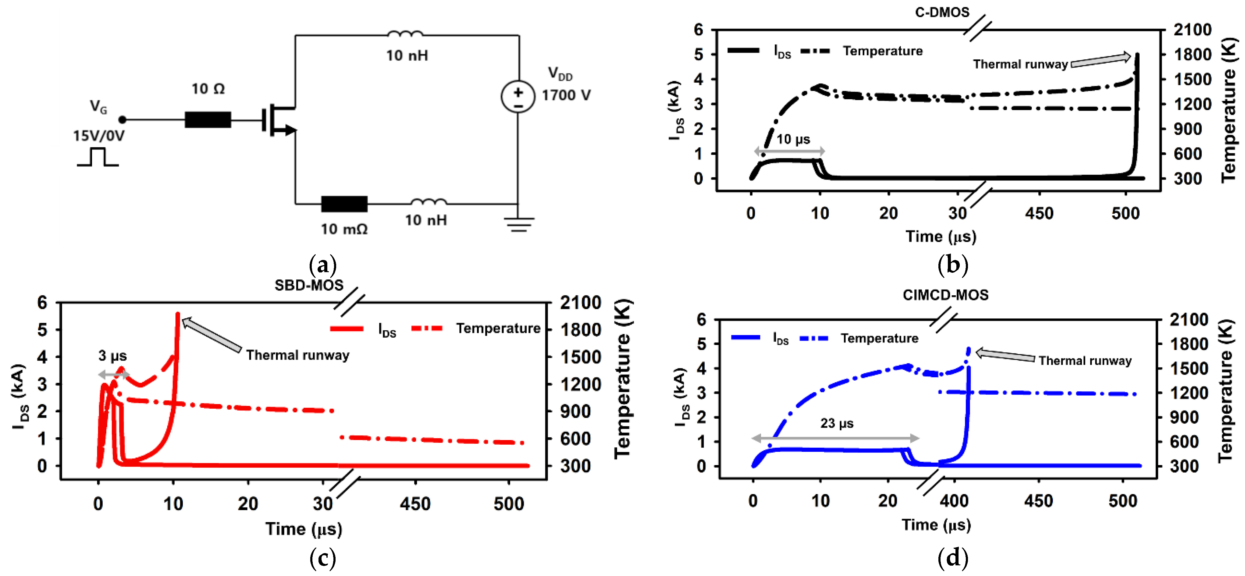
3.2. Dynamic Performances

Next, we simulated the dynamic characteristics of the device via mixed-mode simulation in TCAD. The short-circuit reliability, parasitic gate capacitance, reverse recovery characteristics, and switching performances of the device were simulated. Figure 7a shows the short-circuit (SC) test circuit diagram. The short-circuit roughness was tested at VDS = 1700 V and VGS = 15 V. The thermal runaway time in the short- circuit condition was observed by applying a pulse voltage to the gate for a fixed duration. Figure 7b–d show the SC withstanding capabilities of the C–DMOSFET, SBD–MOSFET, and CIMCD–MOSFET. The temperature represents the highest temperature of the device. In the SBD–MOSFET, when the SC time is 3 µs, the leakage current and the internal temperature of the device rapidly increase in thermal runaway. The SBD–MOSFET has a very short SC withstand time (TSC) of approximately less than 3 µs and the lowest SC reliability. Conversely, the CIMCD–MOSFET has the longest TSC compared to the C–DMOSFET and SBD–MOSFET, where device failure occurred at TSC = 23 µs. TSC is generally inversely proportional to the device’s drain saturation current (IDsat) [48]. Since CIMCD–MOSFETs have a smaller IDsat than C–DMOSFETs, they have the longest SC withstand time and consequently, the highest SC capability. Figure 8 shows the total current density and lattice temperature of the device at the SC thermal runaway point after the gate is turned off. As is evident from Figure 8a,c, the thermal runaway mechanism of the C–DMOSFET and CIMCD–MOSFET results in device failure owing to the drain leakage current that is caused by the parasitic npn transistor turn-on [49]. However, as shown in Figure 8b, the off-state leakage current of the SBD–MOSFET occurs at the Schottky contact. The elevated lattice temperature near the Schottky contact enhances the thermionic-field emission there and moves many electrons, generating a large off-state leakage current even in the gate-off state [50,51]. Consequently, the SBD–MOSFET undergoes early thermal runaway and has a very poor short-circuit capability compared to the CIMCD–MOSFET.
Figure 9 compares the parasitic capacitances Crss (CGD), Ciss (CGD + CGS), and Coss (CGD + CDS) of the C–DMOSFET, SBD–MOSFET, and CIMCD–MOSFET. Crss is an important parameter that has high correlation with the switching time. In general, because the values of Crss are proportional to the switching time, it is advantageous to minimize the values of Crss. As the CIMCD–MOSFET has a split gate structure, the overlap area between the gate-drain can be minimized, thereby reducing the parasitic capacitance that is generated from the gate-drain coupling [52]. Consequently, the CIMCD–MOSFET has a low Crss value that is reduced by 71.06% for the C–DMOSFET and 61.98% for the SBD–MOSFET.
Figure 10a compares the body diode reverse recovery characteristics of the C–DMOSFET, SBD–MOSFET, and CIMCD–MOSFET. Figure 10b shows a double pulsed test circuit to check the reverse recovery and switching characteristics of the device. In Figure 10a, the IRM is the reverse peak current, and the reverse recovery time Trr is the time that is taken by the reverse recovery current to reduce from zero to −IRM and subsequently recover to −0.1 IRM [53]. The reverse recovery charge Qrr can be calculated by integrating the IDS over Trr. As the body diode of the C–DMOSFET operates as a bipolar device, several remaining minority carriers in the N-drift have to be recombined when it is turned off, resulting in a large Qrr. Conversely, in the SBD–MOSFET and CIMCD–MOSFET, because the body diode operates as a unipolar device, a few minority carriers remain in the N-drift, and the Qrr is much smaller than that of the C–DMOSFET. The Qrr of the CIMCD–MOSFET is similar to that of the SBD–MOSFET and is reduced 89.1% from that of C–DMOSFET.
Figure 11 shows the switching transients of the C–DMOSFET, SBD–MOSFET, and CIMCD–MOSFET. Figure 12 compares the power dissipation of each device. The switching-on time TON is defined as the sum of the time from 10% VGS to 90% VDS (Td-on) and the rise time from 90% to 10% VDS (Tr). Similarly, the switching-off time TOFF is defined as the sum of the time from 90% VGS to 10% VDS (Td-off) and the fall time from 10% to 90% VDS (Tf) [54]. As the Crss decreases due to the split gate structure, the CIMCD–MOSFET has a shorter switching time than the C–DMOSFET and SBD–MOSFET. With a short switching time and small Qrr, the switching on and off energy losses (EON, EOFF) of the CIMCD–MOSFET are greatly reduced, and the total switching energy loss (ET) is reduced by 67.8% and 41.8%, respectively, compared to the C–DMOSFET and SBD–MOSFET. Table 3 lists the dynamic characteristics of the C–DMOSFET, SBD–MOSFET, and CIMCD–MOSFET devices.

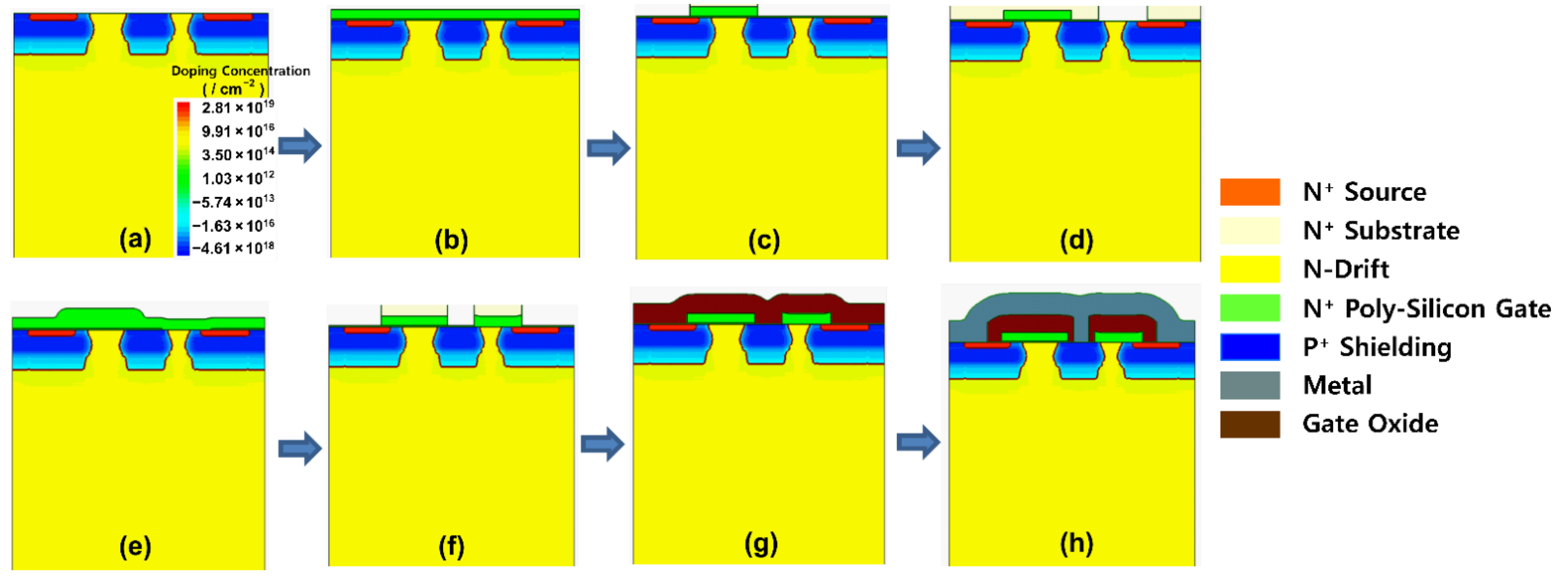
3.3. Proposed Fabrication Process

Figure 13 shows the proposed fabrication process of CIMCD-MOSFET through Sprocess simulation. Figure 13a illustrates the formation of the drift region by SiC epitaxial growth on the N+ substrate, and the formation of the P+ shielding region, p-base region, and source region through multi-ion implantation [55,56]. Next, an oxide film is formed by dry thermal oxidation and doped polysilicon is deposited as shown in Figure 13b [57]. Then, in Figure 13c, the polysilicon is etched by anisotropic etching, leaving only the gate region. After making the thin oxide film (Tox2) of the MOS-channel diode through anisotropic oxide etching in Figure 13d, polysilicon is deposited again as shown in Figure 13e [58]. Subsequently, excluding the gate part and the dummy gate part, the remaining polysilicon region is anisotropically etched as shown in Figure 13f. After that, N inter-level dielectric (ILD) oxide film is deposited through CVD in Figure 13g, and finally, the source contact is completed through metal deposition after etching the source region of the ILD oxide as shown in Figure 13h [59].

4. Conclusions

In this study, a built-in MOS-channel diode MOSFET with a center-doped P+ region was investigated via TCAD simulation. The CIMCD–MOSFET effectively protects the gate oxide owing to the center P+ shielding region that overlaps with the oxide edge. Moreover, this region minimizes static degradation by increasing the doping concentration of the JFET and N-drift via electric field dispersion. In addition, the low saturation current allows CIMCD–MOSFET to exhibit better short-circuit withstanding capability than the C–DMOSFET and the SBD–MOSFET. The reverse recovery charge, similar to that of the SBD and the split gate structure of the device, greatly reduces the switching time and loss of the CIMCD–MOSFET. Consequently, the B–FOM of the CIMCD–MOSFET is improved by 2.05% and 11.17%, and the switching loss is improved by 67.8% and 41.8%, respectively, compared to those of the C–DMOSFET and SBD–MOSFET. These results demonstrate that the CIMCD–MOSFET can be effectively used as a 3.3 kV high-voltage power module system with a body diode configuration owing to its high reliability and improved switching characteristics.

Author Contributions

All authors contributed to this work. Conceptualization, J.N.; methodology, J.N., M.K. and K.K.; software, J.N. and M.K.; validation, J.N., M.K. and K.K.; formal analysis, J.N., M.K. and K.K.; investigation, J.N.; resources, J.N., M.K. and K.K.; writing—original draft preparation, J.N.; writing—review and editing, K.K.; visualization, J.N.; supervision, K.K.; project administration, J.N. and K.K.; All authors have read and agreed to the published version of the manuscript.

Funding

This research received no external funding.

Institutional Review Board Statement

Not applicable.

Informed Consent Statement

Not applicable.

Data Availability Statement

Data are not available on a publicly accessible repository and they cannot be shared under request.

Acknowledgments

This paper was supported by a Korea Institute for Advancement of Technology (KIAT) grant funded by the Korea Government (MOTIE) (P0017011, HRD Program for Industrial Innovation), and then Samsung Electronics.

Conflicts of Interest

The authors declare no conflict of interest.

References

  1. Chow, T.P. Wide bandgap semiconductor power devices for energy efficient systems. In Proceedings of the 2015 IEEE 3rd Workshop on Wide Bandgap Power Devices and Applications (WiPDA), Blacksburg, VA, USA, 2–4 November 2015; pp. 402–405. [Google Scholar]
  2. Cooper, J.A.; Agarwal, A. SiC power-switching devices-the second electronics revolution? Proc. IEEE 2002, 90, 956–968. [Google Scholar] [CrossRef]
  3. Baliga, B.J. Silicon Carbide Power Devices; World Scientific: Singapore, 2006; pp. 15–36. [Google Scholar]
  4. Wang, G.; Wang, F.; Magai, G.; Lei, Y.; Huang, A.; Das, M. Performance comparison of 1200V 100A SiC MOSFET and 1200 V 100 A silicon IGBT. In Proceedings of the 2013 IEEE Energy Conversion Congress and Exposition, Denver, CO, USA, 16–20 September 2013; pp. 3230–3234. [Google Scholar]
  5. Guan, Q.X.; Li, C.; Zhang, Y.; Wang, S.; Xu, D.D.; Li, W.; Ma, H. An Extremely High Efficient Three-Level Active Neutral-Point-Clamped Converter Comprising SiC and Si Hybrid Power Stages. IEEE Trans. Power Electron. 2018, 33, 8341–8352. [Google Scholar] [CrossRef]
  6. Fuentes, C.D.; Kouro, S.; Bernet, S. Comparison of 1700-V SiC-MOSFET and Si-IGBT Modules under Identical Test Setup Conditions. IEEE Trans. Ind. App. 2019, 55, 7765–7775. [Google Scholar] [CrossRef]
  7. Zhang, L.; Yuan, X.; Wu, X.; Shi, C.; Zhang, J.; Zhang, Y. Performance Evaluation of Hgih-Power SiC MOSFET Modules in Comparison to Si IGBT Modules. IEEE Trans. Power Electron. 2019, 34, 1181–1196. [Google Scholar] [CrossRef]
  8. Sabri, S.; Van Brunt, E.; Barkley, A.; Hull, B.; O’Loughlin, M.; Burk, A.; Allen, S.; Palmour, J. New generation 6.5 kV SiC power MOSFET. In Proceedings of the 2017 IEEE 5th Workshop on Wide Bandgap Power Devices and Applications (WiPDA), Albuquerque, NM, USA, 30 October–1 November 2017; pp. 246–250. [Google Scholar]
  9. Sakaguchi, T.; Aketa, M.; Nakamura, T.; Nakanishi, M.; Rahimo, M. Characterization of 3.3 kV and 6.5 kV SiC MOSFETs. In Proceedings of the PCIM Europe 2017, International Exhibition and Conference for Power Electronics, Intelligent Motion, Renewable Energy and Energy Management, Nuremberg, Germany, 16–18 May 2017; pp. 1–5. [Google Scholar]
  10. Horff, R.; März, A.; Lechler, M.; Bakran, M. Optimised switching of a SiC MOSFET in a VSI using the body diode and additional Schottky barrier diode. In Proceedings of the 2015 17th European Conference on Power Electronics and Applications (EPE’15 ECCE-Europe), Geneva, Switzerland, 8–10 September 2015; pp. 1–11. [Google Scholar]
  11. Efthymiou, L.; Camuso, G.; Longobardi, G.; Udrea, F.; Lin, E.; Chien, T.; Chen, M. Zero reverse recovery in SiC and GaN Schottky diodes: A comparison. In Proceedings of the 2016 28th International Symposium on Power Semiconductor Devices and IC’s (ISPSD), Prague, Czech Republic, 12–16 June 2016; pp. 71–74. [Google Scholar]
  12. Dyer, J.; Zhang, Z.; Wang, F.; Costinett, D.; Tolbert, L.M.; Blalock, B.J. Dead-time optimization for SiC based voltage source converters using online condition monitoring. In Proceedings of the 2017 IEEE 5th Workshop on Wide Bandgap Power Devices and Applications (WiPDA), Albuquerque, NM, USA, 30 October–1 November 2017; pp. 15–19. [Google Scholar]
  13. Ahmed, M.R.; Todd, R.; Forsyth, A.J. Switching performance of a SiC MOSFET body diode and SiC schottky diodes at different temperatures. In Proceedings of the 2017 IEEE Energy Conversion Congress and Exposition (ECCE), Cincinnati, OH, USA, 1–6 October 2017; pp. 5487–5494. [Google Scholar]
  14. Badawi, N.; Bahat-Treidel, E.; Dieckerhoff, S.; Hilt, O.; Würfl, J. Evaluation of 600V GaN and SiC Schottky diodes at different temperatures. In Proceedings of the 15th European Conference on Power Electronics and Applications (EPE), Lille, France, 2–6 September 2013; pp. 1–7. [Google Scholar]
  15. Jiang, X.; Wang, J.; Chen, J.; Li, Z.; Zhai, D.; Yang, X.; Bing, J.; Shen, Z.J. Investigation on Degradation of SiC MOSFET Under Surge Current Stress of Body Diode. IEEE J. Emerg. Sel. Top. Power Electron. 2020, 8, 77–89. [Google Scholar] [CrossRef]
  16. Kawahara, K.; Hino, S.; Sadamatsu, K.; Nakao, Y.; Iwamatsu, T.; Nakata, S.; Tomohisa, S.; Yamakawa, S. Impact of Embedding Schottky Barrier Diodes into 3.3 kV and 6.5 kV SiC MOSFETs. Mater. Sci. Forum 2017, 924, 663–666. [Google Scholar] [CrossRef]
  17. Wang, Z.; Ouyang, J.; Zhang, J.; Wu, X.; Sheng, K. Analysis on reverse recovery characteristic of SiC MOSFET intrinsic diode. In Proceedings of the 2014 IEEE Energy Conversion Congress and Exposition (ECCE), Pittsburgh, PA, USA, 14–18 September 2014; pp. 2832–2837. [Google Scholar]
  18. Nayak, D.P.; Yakala, R.K.; Kumar, M.; Pramanick, S.K. Temperature-Dependent Reverse Recovery Characterization of SiC MOSFETs Body Diode for Switching Loss Estimation in a Half–Bridge. IEEE Trans. Power Electron. 2022, 37, 5574–5582. [Google Scholar] [CrossRef]
  19. Tominaga, T.; Hino, S.; Mitsui, Y.; Nakashima, J.; Kawahara, K.; Tomohisa, S.; Miura, N. Superior Switching Characteristics of SiC-MOSFET Embedding SBD. In Proceedings of the 2019 31st International Symposium on Power Semiconductor Devices and IC’s (ISPSD), Shanghai, China, 19–23 May 2019; pp. 27–30. [Google Scholar]
  20. Matsui, K.; Aiba, R.; Yano, H.; Iwamuro, N.; Baba, M.; Harada, S. Comprehensive Study on Electrical Characteristics in 1.2 kV SiC SBD-integrated Trench and Planar MOSFETs. In Proceedings of the 2021 33rd International Symposium on Power Semiconductor Devices and IC’s (ISPSD), Nagoya, Japan, 30 May–3 June 2021; pp. 215–218. [Google Scholar]
  21. Li, X.; Tong, X.; Huang, A.Q.; Tao, H.; Zhou, K.; Jiang, Y.; Jiang, J.; Deng, X.; She, X.; Zhang, B.; et al. SiC Trench MOSFET With Integrated Self-Assembled Three-Level Protection Schottky Barrier Diode. IEEE Trans. Electron Devices 2018, 65, 347–351. [Google Scholar] [CrossRef]
  22. Hsu, F.J.; Yen, C.T.; Hung, C.C.; Hung, H.T.; Lee, C.Y.; Lee, L.S.; Huang, Y.-F.; Chen, T.-L.; Chuang, P.-J. High efficiency high reliability SiC MOSFET with monolithically integrated Schottky rectifier. In Proceedings of the 2017 29th International Symposium on Power Semiconductor Devices and IC’s (ISPSD), Sapporo, Japan, 28 May–1 June 2017; pp. 45–48. [Google Scholar]
  23. Yen, C.T.; Hung, C.C.; Hung, H.T.; Lee, L.S.; Lee, C.Y.; Yang, T.M.; Huang, Y.-F.; Cheng, C.-Y.; Chuang, P.-J. 1700 V/30 A 4H-SiC MOSFET with low cut–in voltage embedded diode and room temperature boron implanted termination. In Proceedings of the 2015 IEEE 27th International Symposium on Power Semiconductor Devices & IC’s (ISPSD), Hong Kong, China, 10–14 May 2015; pp. 265–268. [Google Scholar]
  24. Nicholls, J.; Dimitrijev, S.; Tanner, P.; Han, J. Description and verification of the fundamental current mechanisms in silicon carbide Schottky barrier diodes. Sci. Rep. 2019, 9, 1–9. [Google Scholar] [CrossRef]
  25. Saitoh, H.S.; Kimoto, T.; Matsunami, H. Origin of leakage current in SiC Schottky barrier diodes at high temperature. Mater. Sci. Forum 2004, 457, 997–1000. [Google Scholar] [CrossRef]
  26. Hatakeyama, T.; Kushibe, M.; Watanabe, T.; Imai, S.; Shinohe, T. Optimum Design of a SiC Schottky Barrier Diode Considering Reverse Leakage Current due to a Tunneling Process. Mater. Sci. Forum 2003, 433, 831–834. [Google Scholar] [CrossRef]
  27. Wang, Y.; Ma, Y.-C.; Hao, Y.; Hu, Y.; Wang, G.; Cao, F. Simulation Study of 4H-SiC UMOSFET Structure With P+-PolySi/SiC Shielded Region. IEEE Trans. Electron Devices 2017, 64, 3719–3724. [Google Scholar] [CrossRef]
  28. An, J.; Hu, S. Heterojunction Diode Shielded SiC Split-Gate Trench MOSFET with Optimized Reverse Recovery Characteristic and Low Switching Loss. IEEE Access 2019, 7, 28592–28596. [Google Scholar] [CrossRef]
  29. Liang, S.; Yu, H.; Liu, H.; Wang, Y.; Wang, J. A novel SiC power MOSFET with integrated polySi/SiC heterojunction freewheeling diode. Semicond. Sci. Tech. 2021, 36, 095017. [Google Scholar] [CrossRef]
  30. Yu, H.; Liang, S.; Liu, H.; Wang, J.; Shen, Z.J. Numerical Study of SiC MOSFET With Integrated n-/n-Type Poly-Si/SiC Heterojunction Freewheeling Diode. IEEE Trans. Electron Devices 2021, 68, 4571–4576. [Google Scholar] [CrossRef]
  31. Wang, Y.; Wang, H.; Cao, F.; Wang, H. High Performance of Polysilicon/4H–SiC Dual–Heterojunction Trench Diode. IEEE Trans. Electron Devices 2017, 64, 1653–1659. [Google Scholar] [CrossRef]
  32. Zhou, X.; Gong, H.; Jia, Y.; Hu, D.; Wu, Y.; Xia, T.; Pang, H.; Zhao, Y. SiC Planar MOSFETs With Built-In Reverse MOS-Channel Diode for Enhanced Performance. IEEE J. Electron Devices Soc. 2020, 8, 619–625. [Google Scholar] [CrossRef]
  33. Zhou, X.; Pang, H.; Jia, Y.; Hu, D.; Wu, Y.; Tang, Y.; Xia, T.; Gong, H.; Zhao, Y. SiC Double-Trench MOSFETs With Embedded MOS-Channel Diode. IEEE Trans. Electron Devices 2020, 67, 582–587. [Google Scholar] [CrossRef]
  34. Deng, X.; Xu, X.; Li, X.; Li, X.; Wen, Y.; Chen, W. A Novel SiC MOSFET Embedding Low Barrier Diode With Enhanced Third Quadrant and Switching Performance. IEEE Electron Device Lett. 2020, 41, 1472–1475. [Google Scholar] [CrossRef]
  35. Nguyen, T.-T.; Ahmed, A.; Thang, T.V.; Park, J.-H. Gate Oxide Reliability Issues of SiC MOSFETs Under Short-Circuit Operation. IEEE Trans. Power Electron. 2015, 30, 2445–2455. [Google Scholar] [CrossRef]
  36. Vudumula, P.; Kotamraju, S. Design and Optimization of 1.2-kV SiC Planar Inversion MOSFET Using Split Dummy Gate Concept for High-Frequency Applications. IEEE Trans. Electron Devices 2019, 66, 5266–5271. [Google Scholar] [CrossRef]
  37. Agarwal, A.; Baliga, B.J.; Francois, M.M.A.; Maxwell, E.; Berliner, N.; Papageorge, M. 3.3 kV 4H-SiC Planar-Gate MOSFETs Manufactured using Gen-5 PRESICETM Technology in a 4-inch Wafer Commercial Foundry. In Proceedings of the SoutheastCon 2021, Atlanta, GA, USA, 10–14 March 2021; pp. 1–4. [Google Scholar]
  38. Jiang, H.; Wei, J.; Dai, X.; Ke, M.; Zheng, C.; Deviny, I. Silicon carbide split-gate MOSFET with merged Schottky barrier diode and reduced switching loss. In Proceedings of the 2016 28th International Symposium on Power Semiconductor Devices and IC’s (ISPSD), Prague, Czech Republic, 12–16 June 2016; pp. 59–62. [Google Scholar]
  39. Lee, S.K.; Zetterling, C.M.; Östling, M. Schottky barrier height dependence on the metal work function for p-type Si Schottky diodes. J. Electron. Mater. 2004, 30, 242–246. [Google Scholar] [CrossRef]
  40. Yi, B.; Wu, Z.; Zhang, Q.; Cheng, J.J.; Huang, H.M.; Pan, Y.L.; Zhang, X.K.; Xiang, Y. A low loss single-channel SiC trench MOSFET with integrated trench MOS barrier Schottky diode. Semicond. Sci. Technol. 2021, 36, 075006. [Google Scholar] [CrossRef]
  41. Vudumula, P.; Kotamraju, S. Design and Optimization of SiC Super-Junction MOSFET Using Vertical Variation Doping Profile. IEEE Trans. Electron Devices 2019, 66, 1402–1408. [Google Scholar] [CrossRef]
  42. Hatakeyama, T.; Nishio, J.; Ota, C.; Shinohe, T. Physical Modeling and Scaling Properties of 4H-SiC Power Devices. In Proceedings of the 2005 International Conference on Simulation of Semiconductor Processes and Devices, Tokyo, Japan, 1–3 September 2005; pp. 171–174. [Google Scholar]
  43. Synopsys, Inc. TCAD SentaurusTM Device User Guide; Synopsys, Inc.: Mountain View, CA, USA, 2017. [Google Scholar]
  44. Ueno, K.; Asai, R.; Tsuji, T. 4H-SiC MOSFETs utilizing the H2 surface cleaning technique. IEEE Electron Device Lett. 1998, 19, 244–246. [Google Scholar] [CrossRef]
  45. An, J.; Hu, S. Experimental and Theoretical Demonstration of Temperature Limitation for 4H-SiC MOSFET during Unclamped Inductive Switching. IEEE J. Emerg. Sel. Top. Power Electron. 2020, 8, 206–214. [Google Scholar] [CrossRef]
  46. Schoen, K.P.; Woodall, J.M.; Cooper, J.A.; Melloch, M.R. Design considerations and experimental analysis of high-voltage SiC Schottky barrier rectifiers. IEEE Trans. Electron Devices 1998, 45, 1595–1604. [Google Scholar] [CrossRef]
  47. Jiang, H.; Wei, J.; Dai, X.; Ke, M.; Deviny, I.; Mawby, P. SiC Trench MOSFET With Shielded Fin-shaped Gate to Reduce Oxide Field and Switching Loss. IEEE Electron Device Lett. 2016, 37, 1324–1327. [Google Scholar] [CrossRef]
  48. Han, K.; Kanale, A.; Baliga, B.J.; Ballard, B.; Morgan, A.; Hopkins, D.C. New Short Circuit Failure Mechanism for 1.2kV 4H-SiC MOSFETs and JBSFETs. In Proceedings of the 2018 IEEE 6th Workshop on Wide Bandgap Power Devices and Applications (WiPDA), Atlanta, GA, USA, 31 October–2 November 2018; pp. 108–113. [Google Scholar]
  49. Namai, M.; An, J.; Yano, H.; Iwamuro, N. Investigation of short-circuit failure mechanisms of SiC MOSFETs by varying DC bus voltage. Jpn. J. Appl. Phys. 2018, 57, 074102. [Google Scholar] [CrossRef]
  50. Okawa, M.; Aiba, R.; Kanamori, T.; Kobayashi, Y.; Harada, S.; Yano, H.; Iwamuro, N. First Demonstration of Short–Circuit Capability for a 1.2 kV SiC SWITCH–MOS. IEEE J. Electron Devices Soc. 2019, 7, 613–620. [Google Scholar] [CrossRef]
  51. Aiba, R.; Matsui, K.; Baba, M.; Harada, S.; Yano, H.; Iwamuro, N. Demonstration of Superior Electrical Characteristics for 1.2 kV SiC Schottky Barrier Diode-Wall Integrated Trench MOSFET With Higher Schottky Barrier Height Metal. IEEE Electron Device Lett. 2020, 41, 1810–1813. [Google Scholar] [CrossRef]
  52. Jiang, J.-Y.; Huang, C.-F.; Wu, T.-L.; Zhao, F. Simulation Study of 4H–SiC Trench MOSFETs with Various Gate Structures. In Proceedings of the 2019 Electron Devices Technology and Manufacturing Conference (EDTM), Singapore, 12–15 March 2019; pp. 401–403. [Google Scholar]
  53. Yue, K.; Pang, L.; You, H.; Li, S.; Kong, D.; Li, Y.; Zhang, Q.; Liu, L. Reverse recovery characteristics of high power thyristors in HVDC converter valve. IEEE Trans. Dielectr. Electr. Insul. 2017, 24, 2132–2140. [Google Scholar] [CrossRef]
  54. Tian, K.; Hallén, A.; Qi, J.; Ma, S.; Fei, X.; Zhang, A.; Liu, W. An Improved 4H-SiC Trench-Gate MOSFET With Low On-Resistance and Switching Loss. IEEE Trans. Electron Devices 2019, 66, 2307–2313. [Google Scholar] [CrossRef]
  55. Shen, H.-J.; Tang, Y.-C.; Peng, Z.-Y.; Deng, X.-C.; Bai, Y.; Wang, Y.-Y.; Li, C.-Z.; Liu, K.-A.; Liu, X.-Y. Fabrication and Characterization of 1700 V 4H-SiC Vertical Double-Implanted Metal-Oxide-Semiconductor Field-Effect Transistors. Chin. Phys. 2015, 32, 127101. [Google Scholar] [CrossRef]
  56. Singh, R.; Capell, D.; Das, M.; Lipkin, L.; Palmour, J. Development of high-current 4H-SiC ACCUFET. IEEE Trans. Electron Devices 2003, 50, 471–478. [Google Scholar] [CrossRef]
  57. Han, K.; Baliga, B.J.; Sung, W. Split-Gate 1.2-kV 4H-SiC MOSFET: Analysis and Experimental Validation. IEEE Electron Device Lett. 2017, 38, 1437–1440. [Google Scholar] [CrossRef]
  58. Johnson, M.B.; Zvanut, M.E.; Richardson, O. HF chemical etching of SiO2 on 4H and 6H SiC. J. Electron. Mater. 2000, 29, 368–371. [Google Scholar] [CrossRef]
  59. Yano, H.; Hatayama, T.; Yraoka, Y.; Fuyuki, T. Characterization of 4H-SiC MOSFETs with NO-annealed CVD oxide. Mater. Sci. Forum 2006, 527, 971–974. [Google Scholar] [CrossRef]
Figure 1. Cross–sectional view of (a) C–DMOSFET, (b) SBD–MOSFET, and (c) CIMCD–MOSFET.
Energies 15 06960 g001
Figure 2. Comparison of the (a) B–FOM characteristics for WJFET and ND variation of CIMCD–MOSFET (b) third-quadrant characteristics for different WD of CIMCD–MOSFET.
Energies 15 06960 g002
Figure 3. Off-state characteristics of C–DMOSFET, SBD–MOSFET, and CIMCD–MOSFET at T = 300 K and 450 K.
Energies 15 06960 g003
Figure 4. Electric field distribution of (a) C–DMOSFET, (b) SBD–MOSFET, (c) CIMCD–MOSFET, and (d) MCD–MOSFET without the center implant region.
Energies 15 06960 g004
Figure 5. On-state characteristics of C–DMOSFET, SBD–MOSFET, and CIMCD–MOSFET.
Energies 15 06960 g005
Figure 6. (a) Third quadrants characteristics of C–DMOSFET, SBD–MOSFET, and CIMCD–MOSFET. (b) Variation of diode turn-on voltage (VF) and oxide edge maximum electric field of CIMCD-MOSFET with Tox2.
Energies 15 06960 g006
Figure 7. (a) Equivalent circuit diagram of short-circuit test. Short-circuit waveforms of (b) C–DMOSFET, (c) SBD–MOSFET, and (d) CIMCD–MOSFET.
Energies 15 06960 g007
Figure 8. Total current density distribution and lattice temperature distribution at the SC thermal runaway point (@IDS = 1 kA/cm2) of (a) C–DMOSFET (b) SBD–MOSFET, and (c) CIMCD–MOSFET.
Energies 15 06960 g008
Figure 9. Comparison of the parasitic gate capacitance of the C–DMOSFET, SBD–MOSFET, and CIMCD–MOSFET.
Energies 15 06960 g009
Figure 10. (a) Comparison of the reverse recovery characteristics of the C–DMOSFET, SBD–MOSFET, and CIMCD–MOSFET. (b) Double pulsed test circuit diagram.
Energies 15 06960 g010
Figure 11. (a) Comparison of the (a) drain voltage switching waveforms and (b) drain current switching waveforms of C–DMOSFET, SBD–MOSFET, and CIMCD–MOSFET.
Energies 15 06960 g011
Figure 12. Comparison of the (a) power dissipation and (b) total switching energy loss of C–DMOSFET, SBD–MOSFET, and CIMCD–MOSFET that were obtained via the double pulsed test.
Energies 15 06960 g012
Figure 13. Proposed fabrication process of CIMCD–MOSFET. (a) The drift region is formed through epitaxyial growth on an N+ SiC substrate, and P+ shielding, P base, and N+ source are formed through multi-implantation. (b) An oxide film is formed through dry oxidation and doped polysilicon is deposited by CVD. (c) Anisotropic polysilicon etching to form a gate region. (d) Anisotropic etching of SiO2 to form a thin oxide film. (Tox2) (e) Deposition of polysilicon through CVD. (f) Anisotropic etch polysilicon to form a dummy gate. (g) Deposition of inter-level dielectric (ILD) oxide through CVD. (h) Etching the oxide and metallization.
Energies 15 06960 g013
Table 1. Device parameters.
ParameterC–SBD–CIMCD–
Cell pitch [μm]910.810.55
Gate oxide thickness Tox1 [nm]505050
Gate oxide thickness Tox2 [nm]--5
P channel width [μm]0.50.50.5
P+ base width [μm]333
P+ base depth [μm]111
N-drift thickness [μm]303030
N+ substrate thickness [μm]100100100
WJFET [μm]32.81.8
WD [μm]-11
WF [μm]--1.75
N-drift doping ND [cm3]2.8 × 10153 × 10153.5 × 1015
JFET doping [cm3]--2 × 10¹⁶
P+ doping [cm3]2 × 10182 × 10182 × 1018
P channel doping [cm3]2 × 10172 × 10172 × 1017
N+ substrate doping [cm3]1 × 10191 × 10191 × 1019
Table 2. Static characteristics of devices.
ParameterC–SBD–CIMCD–
BV [V]408939264045
RON-SP [mΩ·cm2]9.810.619.4
EMOX (@VDS = 3 kV) [MV/cm]33.072.34
B–FOM [kV2/mΩ·cm2]1.7061.5661.741
VF (@IDS = −80 A·cm2) [μm]3.271.812.44
Table 3. Dynamic characteristics of devices.
ParameterC–SBD–CIMCD–
TSC [µs]<10<3<23
Crss [pF·cm2]37.9428.8810.98
Trr [ns]11470.442.2
IRM [A/cm2]1673545
Qrr [µC·cm2]10.691.021.17
TON [ns]13912292
TOFF [ns]1206991551
EON [mJ·cm2]25.4811.449.28
EOFF [mJ·cm2]17.2612.224.48
ET [mJ·cm2]42.7423.6613.76
Publisher’s Note: MDPI stays neutral with regard to jurisdictional claims in published maps and institutional affiliations.

