Article

Research on Single-Phase and Three-Phase Compatible Isolated On-Board Charger and Control Technology

Engineering Research Center of Automotive Electronics Drive Control and System Integration, Ministry of Education, Harbin University of Science and Technology, Harbin 150080, China
*
Author to whom correspondence should be addressed.
Energies 2022, 15(17), 6445; https://doi.org/10.3390/en15176445
Submission received: 30 July 2022 / Revised: 29 August 2022 / Accepted: 1 September 2022 / Published: 3 September 2022

Abstract

:
This paper presents a single-phase and three-phase compatible isolated on-board charger for electric vehicles. The charger is compatible with the single-phase and three-phase AC voltage input and is composed of two-stage circuits. Based on the three-phase six-switch power factor correction (PFC) circuit, by switching on and off, the front stage is transformed into a cascade topology of a totem-pole PFC circuit and boost circuit. The rear stage is a full-bridge LLC resonant converter. In the single-phase or three-phase working mode, the front-stage control strategy is a double closed-loop control. The current inner loop controller is improved for the three-phase six-switch PFC circuit. The PI controller and repetitive controller are connected in parallel to form the current inner loop compound controller, which can effectively reduce the total harmonic distortion of the input current. By using simulation software MATLAB/Simulink, the circuit model was built. The simulation results verify the correctness of the theoretical analysis.

1. Introduction

With the development of the automobile industry, electric vehicles have gradually been promoted. The electric vehicle draws energy from the AC grid through the on-board charger (OBC) and charges the power battery after the electric energy is transformed. Therefore, the OBC is an important part of electric vehicles [1]. The input power supply of OBC mainly includes single-phase AC voltage and three-phase AC voltage. At present, most OBCs mainly work under single-phase input conditions, with low output power and long charging time. With the increase in the capacity of the power battery of new energy vehicles and the demand for faster charging, the market demand for three-phase input high-power car chargers is also increasing [2]. The design of the OBC should be compatible with single-phase and three-phase power inputs so that electric vehicles can meet the use of different power occasions through flexible charging.
The early OBC is the single-stage structure, which has the advantages of a simple circuit structure and convenient control, but its efficiency and power factor are difficult to achieve satisfactory results, and the output voltage range is narrow [3]. Nowadays, the mainstream topology of OBC is mainly composed of a front-stage power factor correction (PFC) circuit and a rear-stage isolated DC–DC circuit. The front-stage PFC circuit can realize PFC, reduce harmonic pollution, and provide the rear-stage DC–DC circuit with a smaller ripple DC bus voltage. The rear stage can output stable and adjustable high-voltage DC supply power to the power battery [4]. Reference [5] proposes a two-stage OBC consisting of a single-phase bridgeless boost PFC circuit and a full-bridge LLC resonant converter. Through the cascade control strategy between modules, the two-stage structure circuit can be started smoothly, the shock in the starting process is eliminated, and the output voltage has no drastic impact. However, the traditional bridgeless PFC circuit has an obvious common mode interference problem. Reference [6] using SiC-MOSFET to design the interleaved parallel totem-pole bridgeless PFC circuit in continuous current mode (CCM) can effectively overcome the common mode interference problem and improve efficiency. Reference [7] designed a 1 kW OBC based on SiC-MOSFET. The front stage of the circuit is a single-ended primary-inductor converter (SEPIC) PFC converter, and the rear stage is a full-bridge LLC resonant converter. Among them, the SEPIC PFC converter can make the DC bus voltage follow the battery pack voltage so that the LLC resonant converter can keep operating near the resonant frequency to realize the optimization of the operating efficiency of the whole machine. The total efficiency from 20% of the rated load to full load is 88.5% to 93.5%. Reference [8] proposes a passive auxiliary converter structure with a three-phase 380 V AC input. The front-stage three-phase six-switch circuit can effectively suppress voltage spikes, and the electric energy can be transferred to the load by itself, thereby reducing the stress of the main circuit. Reference [9] designed a three-phase bidirectional isolated soft-switch OBC. The front stage is a bidirectional 3-phase 4-switch rectifier. Compared with the common three-phase bridge rectifier, the number of switch tubes is reduced by two, which reduces the complexity of the control circuit. The rear stage is a double-bridge series resonant converter with phase-shift control, which can realize bidirectional power flow. However, the topologies proposed in the reference [5,6,7,8,9] can only meet the power supply mode of a single-phase or three-phase input. In recent years, some OBC topologies that can satisfy single-phase and three-phase compatible inputs have been proposed [10,11,12,13]. Reference [10] proposed a modular single-stage electrolytic capacitorless OBC compatible with single-phase and three-phase voltage input, and used relays and decoupling capacitors to transform single-phase and three-phase circuit topologies. Reference [11] proposes a variable front-stage OBC with dual closed-loop interval type II fuzzy control. Based on the interleaved parallel totem pole bridgeless PFC circuit, the third bridge arm and the corresponding control switch are added to design the front stage variable PFC circuit, and the rear stage adopts the full bridge LLC resonant converter. The feasibility of the proposed topology scheme being compatible with a single and three-phase input is verified by simulation experiments. Generally speaking, the DC bus voltage of the single-phase PFC circuit is usually set at about 400 V, and the output DC bus voltage of the three-phase PFC circuit is usually set at about 700~800 V. However, the variable circuit of the front stage proposed in the reference [11] cannot meet the same output voltage of the DC bus, so it will bring inconvenience to the parameter design of the rear stage circuit. Reference [12] considers the efficiency of the rear-stage DC–DC circuit, combined with the requirements of the same DC bus, and uses the relay to achieve a VIENNA topology compatible with different power supply methods. Reference [13] designs the front-stage compatible PFC circuit of OBC. The rectifier has extended voltage gain characteristics in the case of single-phase input and can convert the input AC voltage of 110 V into high-voltage DC of 750 V, realize the same DC bus voltage in the two input modes, and achieve 93.6% efficiency at full load.
As a key technology of OBC, the control strategy directly determines the operation efficiency, battery life, and charging safety of OBC. For the control system of single and three-phase PFC circuits, the double closed-loop PI control strategy using the current inner loop and the voltage outer loop is the most common. However, when the traditional double closed-loop PI control strategy is applied to the three-phase PFC circuit, it is easy to have some problems, such as waveform distortion and an uneven current. Reference [14] adopts a fractional-order PID control strategy to improve steady-state control accuracy and reduce ripple. The results show that the control performance of the system is enhanced, and the steady-state and dynamic performance is improved, but the parameter tuning process is more complicated. Reference [15] proposed an adaptive cosine inner membrane control method to suppress grid-side current harmonics based on traditional PI control, which effectively suppressed the low-frequency harmonics of the grid-side current. Reference [16] analyzed the shortcomings of traditional PI control, where a simplified form of control transfer functions based on the small-signal model was proposed with segmented control action. The methodology has the advantages of both simplified control strategies and segmented PI-repetitive control to achieve high-power factor performance and reduce THD in a broad range of load conditions.
The parameter design of the rear-stage DC–DC circuit is affected by the DC bus voltage output of the front stage. If the DC bus voltage can be the same in the two power supply modes, it will be conducive to the optimal design of the overall circuit. Inspired by the above references, after the rear-stage circuit is determined to be a full-bridge LLC resonant converter, in order to realize the same DC bus voltage under two power supply modes, a two-stage OBC topology that can realize the compatible input of single-phase and three-phase AC voltage is proposed. Based on the three-phase six-switch PFC circuit topology, the front stage transforms into a cascade topology structure of a totem-pole PFC circuit and boost circuit through switching on and off. After the design of compatible inductors and compatible capacitors, the PFC circuit can achieve a compatible input of single-phase and three-phase voltages and provide the same DC input voltage for the rear-stage full-bridge LLC resonant converter. The full-bridge LLC resonant converter establishes an equivalent model through the fundamental wave analysis method and obtains the optimal parameters of the circuit. Aiming at the control strategy of the front-stage three-phase PFC circuit, the current inner loop controller is improved, and the current inner loop PI controller and the repetitive controller are connected in parallel to form the current inner loop compound controller. Compared with the traditional double closed-loop PI control, it can effectively reduce the THD rate of the grid-side current under different load conditions.

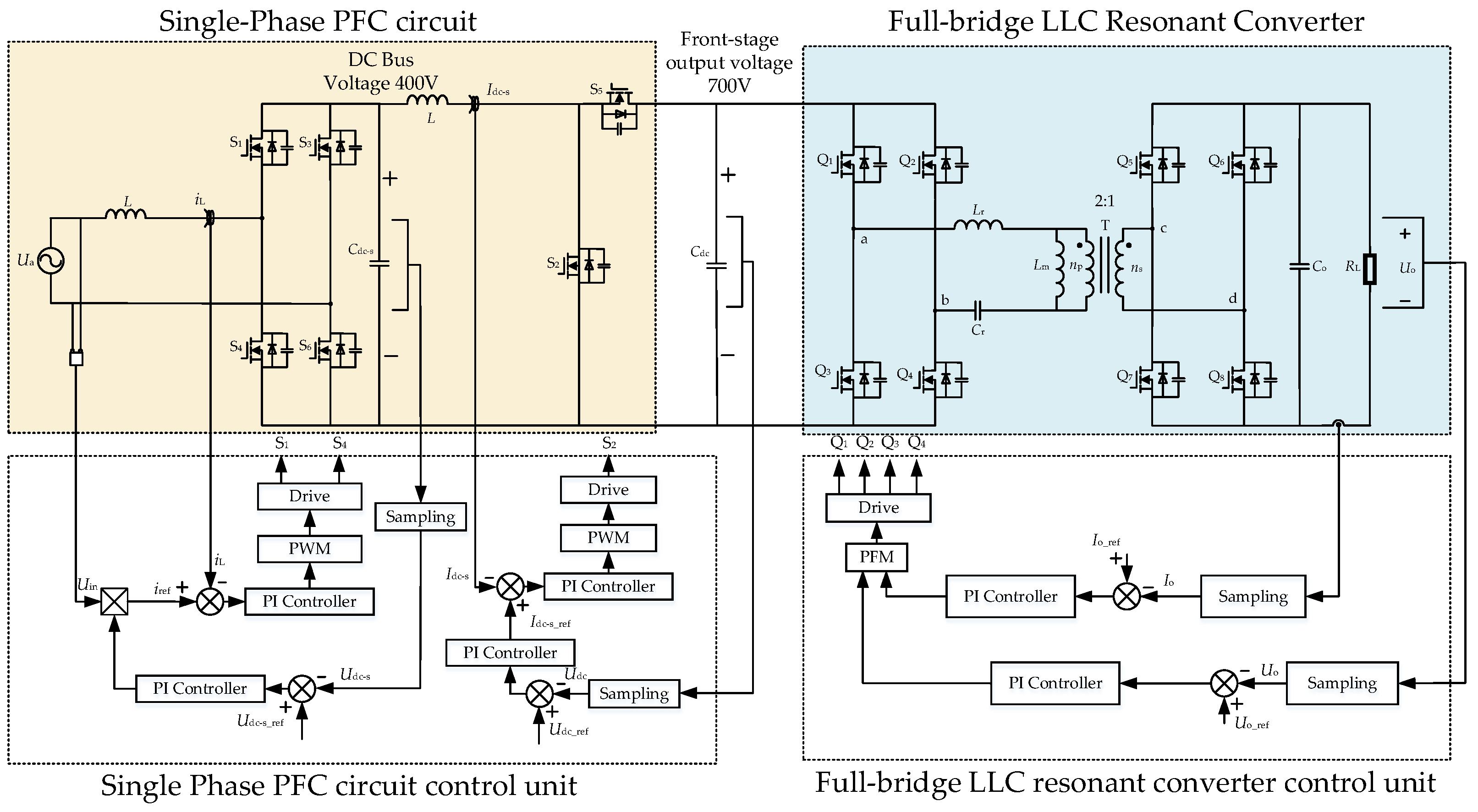
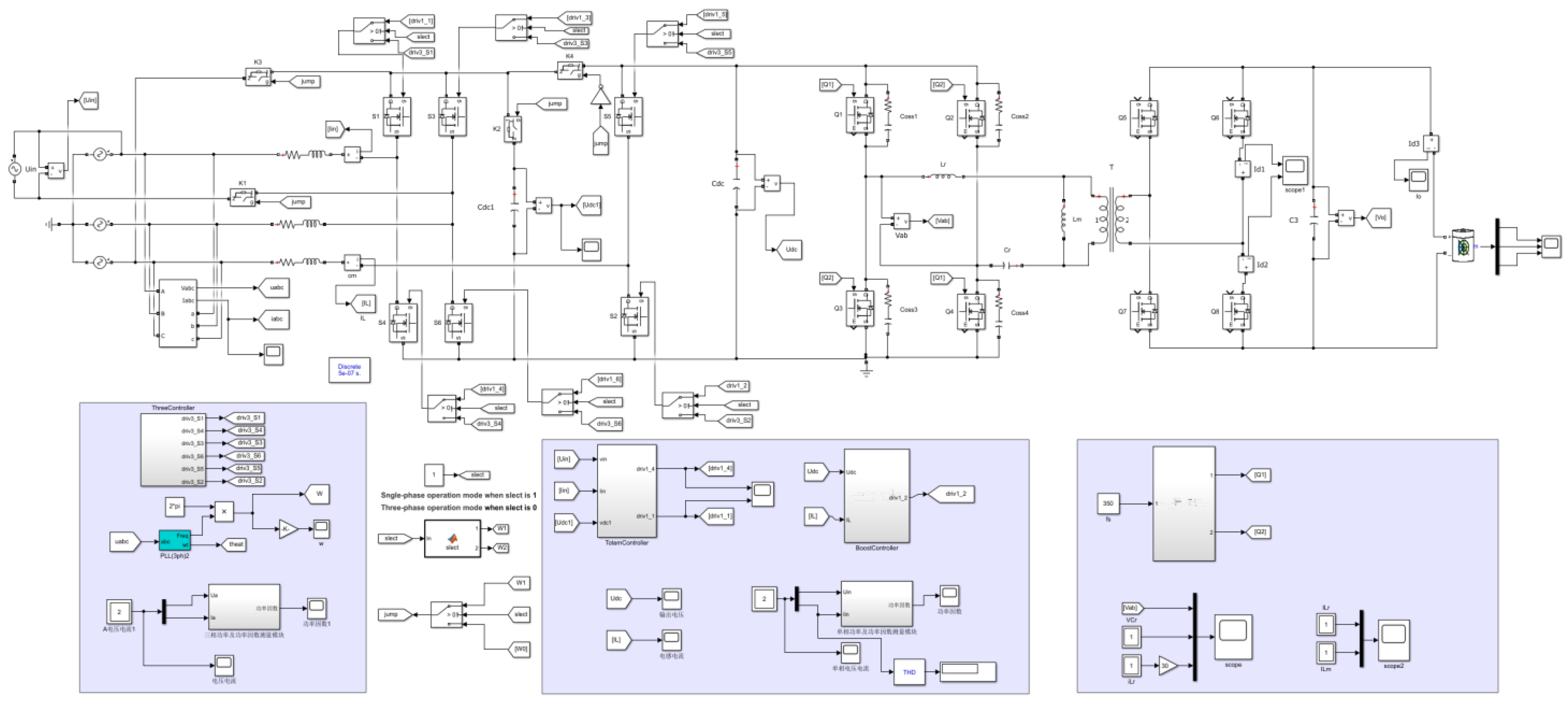
2. Topological Structure and Working Principle of the OBC System

Figure 1 shows the basic topology of a single-phase and three-phase compatible isolated OBC. Single-phase and three-phase topology was switched through relays K1K4. When the front stage was a three-phase voltage input, K1K3 was open and K4 was closed. The topology was a three-phase six-switch PFC circuit. When the front stage was a single-phase voltage input, K1K3 was closed and K4 was open. The topology was a combination circuit of a totem-pole PFC circuit cascaded boost circuit, and the rear stage was a full-bridge LLC resonant converter. The front-stage PFC circuit included an AC inductor L, field-effect transistors (FETs) S1–S6 (SiC-MOSFET), and DC bus capacitances Cdc-s and Cdc. The rear-stage LLC resonant converter included FETs Q1–Q8, resonant capacitance Cr, resonant inductor Lr, excitation inductance Lm, transformer T, holding capacitance Co, and load equivalent resistance RL.

2.1. Three-Phase Working Mode

Figure 2 shows the charging circuit in the three-phase working mode. The front stage was the three-phase six-switch PFC circuit, which can essentially be equivalent to three pulse-width modulation (PWM) rectifiers. Ua, Ub, and Uc were the three-phase input grid voltage, and the AC inductance La = Lb = Lc = L.
The switching function shown in Equation (1) was used to represent an off-conduction state of the FET, and then the operating state of the six FETs of the three-phase bridge arm.
S k = { 1 The   upper   bridge   arm   is   on ,   the   lower   bridge   arm   is   off 0 The   upper   bridge   arm   is   off ,   the   lower   bridge   arm   is   on } k = a , b , c
It can be seen from Equation (1) that there were a total of eight switch state combinations of SaSbSc = 000, SaSbSc = 001, SaSbSc = 010, SaSbSc = 011, SaSbSc = 100, SaSbSc = 101, SaSbSc = 110, and SaSbSc = 111, corresponding to the path topology of different PWM rectifier converters. By controlling the on–off of S1–S6, the input current was in phase with the input voltage, and the waveform was similar to a sine wave, so as to achieve the purpose of PFC.
The rear stage was the full-bridge LLC resonant converter, which converts the high-voltage DC transmitted from the front-stage PFC circuit into high-frequency voltage pulses. The resonant converter converts the high-frequency voltage pulse into sine wave voltage, and finally converts the sine wave voltage into DC voltage output through the rectifier circuit [17]. According to the charging protocol curve of the OBC, the output voltage variation range is controlled by changing the switching frequency of Q1–Q4.

2.2. Single-Phase Working Mode

Figure 3 shows the charging circuit in the single-phase working mode. The front stage was the topology of the cascade of the totem-pole PFC circuit and boost circuit. The use of SiC-MOSFET enabled the totem-pole PFC circuit to achieve higher efficiency and can work in CCM. When three-phase AC voltage was input, the DC output voltage after passing through the three-phase six-switch PFC circuit was Udc, and its rated value was 700 V. When single-phase AC voltage was input, it could output a stable DC voltage Udc-s after passing through the totem-pole PFC circuit, and its rated value was 400 V. To make the input voltage of the rear-stage full-bridge LLC resonant converter have the same value in the two input modes, a boost circuit was added after the totem-pole PFC circuit to increase the DC voltage from 400 V to 700 V.
When the totem-pole PFC circuit is in a steady-state operation, a power cycle can be divided into four modes, and the working modes of the positive and negative cycles are similar. The two modes of the positive half cycle of the AC input power were taken as an example. For mode one, turn off S1 and S3, turn on S4 and S6, Ua charges La through La, S4, and S6 loops, and Cdc-s discharges the subsequent circuit. For mode two, turn off S3 and S4, turn on S1 and S6, Ua and La charge Cdc-s through the S1 and S6 circuits, and La is in a discharged state at this time. When the boost circuit part is in a steady-state operation, it can be divided into two working modes. That is, when S2 is turned on, Udc-s charges Lc; when S2 is turned off, Udc-s and Lc charge Cdc through the S5 loop, and Lc is in a discharged state at this time.

3. Parameter Design

The performance indicators of OBC are the main reference for the design of circuit parameters. According to the main performance indicators shown in Table 1, the parameter design should be carried out in the case of the rated output power of single-phase 3.3 kW and three-phase 6.6 kW.

3.1. Parameter Design of the Front-Stage PFC Circuit

(1)
AC inductance L
When the single-phase voltage was input, for the totem-pole PFC circuit, the selection of L required that the maximum value of the input current ripple was less than 10% of the maximum input current. The calculation is expressed as:
U dc-s T sw 8 L < 10 % 2 P o-s η U in _ min ,
where Udc-s is the DC bus voltage, Udc-s = 400 V; Tsw is the switching period, Tsw = 20 μs; Po-s is the rated output power in single-phase operation, Po-s = 3.3 kW; η is the efficiency, η = 93%; and Uin_min is the minimum input voltage, Uin_min = 176 V.
From Equation (2), L > 0.36 mH was obtained.
For the boost circuit, when the inductor current was in the CCM state, the selection of the AC inductor needed to satisfy Equation (3):
L = U dc-s D ( 1 D ) γ f sw I omin = 400 × 0.43 × ( 1 0.43 ) 2 × 50 × 10 3 × 4 = 0.25   mH ,
where D is the duty cycle; γ is the current ripple coefficient; and Iomin is the critical continuous load current.
From Equation (3), if the inductor current was required to work in continuous mode, L > 0.25 mH.
When the three-phase voltage was input, L was determined by the AC current following the performance index and the current harmonic suppression performance index. The calculation is expressed as:
U m T sw ( 2 U dc 3 U m ) 2 U dc Δ i max L 2 U dc 3 ω I m ,
where Um is the phase voltage fundamental wave, Um = 311 V; Udc is the output voltage of the front stage, Udc = 700 V; Im is the fundamental peak value of phase current, Im = 19 A; and Δimax is the maximum peak value of current ripple, Δimax = 20%Im = 3.8 A.
From Equation (4), 0.55 mH ≤ L ≤ 78.2 mH.
Based on the actual situation and simulation experiment, take L = 1 mH.
(2)
DC bus capacitance Cdc-s
When the single-phase voltage was input, for the totem-pole PFC circuit, the choice of the Cdc-s was mainly determined by the low-frequency voltage ripple and the load holding time, which needed to meet Equations (5) and (6). The holding time Δt was the time required for Udc-s to drop from the rated voltage to β% of the rated voltage after the power outage.
C dc-s P o-s ω U ripple-s U dc-s 2 = 3300 2 × π × 50 × 10 × 400 2 = 2626.06   μ F ,
where Uripple-s is the ripple value of the Udc-s.
C dc-s 2 P o-s Δ t U dc-s 2 ( β % U dc-s ) 2 = 2 × 3300 × 0.02 400 2 ( 0.8 × 400 ) 2 = 2291.67   μ F ,
where Δt = 0.02 s; β% = 80%.
According to Equations (5) and (6), Cdc-s ≥ 2626.06 μF. Based on the actual situation and simulation experiment, take Cdc-s = 2700 μF.
(3)
DC bus capacitance Cdc
In the case of single-phase input voltage, Cdc is part of the boost circuit parameters, and the selection of capacitance mainly controls the output ripple within the specified range. In CCM, the capacitance depends on the output current, switching frequency, and desired output voltage ripple value. Therefore, the capacitance value can be selected according to Equation (7):
C dc I o max D f sw U ripple = 4.71 × 0.43 50 × 10 3 × 14 = 2.89   μ F ,
where Iomax is the maximum output current; and Uripple is the ripple value of Udc.
When the three-phase voltage was input, the larger the value of Cdc, the smaller the Uripple and the stronger the anti-load disturbance ability. However, if the value is too large, it will affect the following performance of the voltage outer loop. Therefore, the selection of Cdc mainly needed to meet the maximum output power and the response time of the voltage loop. The calculation is expressed as:
C dc P o T r 2 U dc U ripple = 6600 × 0.001 2 × 700 × 14 = 336.73   μ F ,
where Tr is the response time of the voltage loop, and Po is the rated output power during three-phase operation.
Based on the actual situation and simulation experiment, take Cdc = 2000 μF.

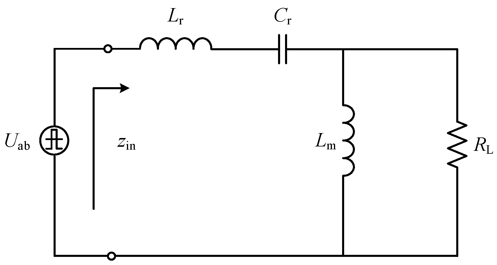
3.2. Parameter Design of the Rear-Stage Full-Bridge LLC Resonant Converter

Voltage gain is an important characteristic of the LLC resonant converter. A fundamental wave analysis was used to analyze the gain characteristic of the LLC resonant converter [18]. The equivalent circuit of the rear-stage LLC resonant converter is shown in Figure 4.
The normalized voltage gain M can be expressed as:
M ( f n , L n , Q e ) = 1 ( 1 + 1 L n 1 L n f n 2 ) 2 + Q e 2 ( f n 1 f n ) 2 ,
where fn is the normalized frequency; Qe is the quality factor; and Ln is the inductance coefficient.
Figure 4 shows that the input impedance Zin of the rear-stage LLC resonant converter is expressed as:
Z i n = L r C r [ L n 2 1 + Q e 2 f n 2 L n 2 + j ( f n - 1 f n + f n L n 1 + Q e 2 f n 2 L n 2 ) ] ,
When the imaginary part of Zin is zero, the maximum quality factor of the converter working in the inductive region can be expressed as:
Q e _ max = 1 L n ( 1 f n 2 ) 1 f n 2 L n 2 .
(1)
Transformer ratio n
The transformer ratio is expressed as:
n = U dc U o _ nor = 2 ,
where Uo_nor is the rated output voltage, Uo_nor = 350 V.
(2)
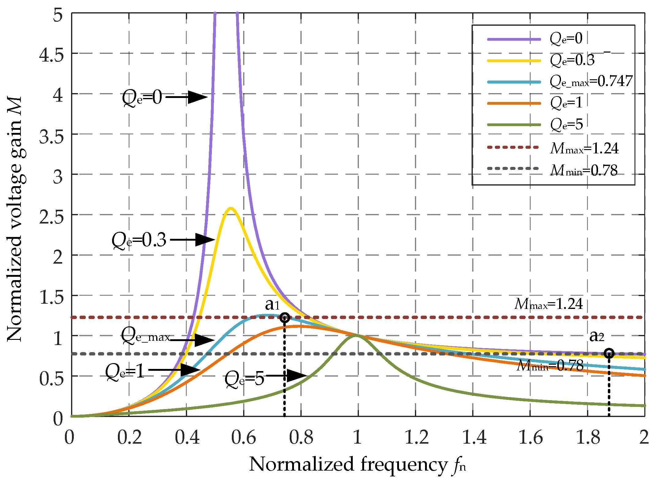
Maximum gain Mmax and minimum gain Mmin
When Udc is minimum and Uo is maximum, the maximum gain Mmax is expressed as:
M max = n U o _ max U dc _ min = 1.24 ,
where Uo_max is the maximum output voltage, Uo_max = 420 V; and Udc_min is the minimum front-stage output voltage, Udc_min = 680 V.
When Udc is maximum and Uo is minimum, the minimum gain Mmin is expressed as:
M min = n U o _ min U dc _ max = 0.78 ,
where Uo_min is the minimum output voltage, Uo_min = 280 V; and Udc_max is the maximum front-stage output voltage, Udc_max = 720 V.
(3)
Inductance coefficient Ln
When the Ln is larger, the amplitude of voltage gain is smaller, causing the working frequency range of the resonant converter to widen. When the Ln is smaller, the excitation current is larger, the turn-off loss of the FET increases, and the efficiency of the converter decreases. Generally, the empirical value of the Ln is between 1–6, and Ln = 2.5 was selected in this design.
(4)
Quality factor Qe
From the impedance characteristics of the rear-stage LLC resonant converter, the maximum quality factor Qe_max can be expressed as:
Q e _ max = 1 L n M max L n + M max 2 M max 2 1 0.747 ,
The value of the quality factor is Qe = 0.95 Qe_max,
Q e = 0.95 Q e _ max 0.71 .
(5)
Maximum operating frequency and minimum operating frequency
Figure 5 exhibits the characteristic operating curve of normalized voltage gain M with normalized frequency fn when Ln = 2.5.
When the quality factor Qe = 0, the LLC resonant converter is in a no-load operation state. The intersection of normalized voltage gain curve and minimum voltage gain curve is a2, and its abscissa is the maximum normalized frequency. The maximum switching frequency is expressed as:
f s _ max = f r 1 L n M min 1 M min + 1 184   kHz ,
where fr is the resonant frequency, fr = 100 kHz.
When the quality factor Qe = Qe_max, the intersection of the normalized voltage gain curve and the maximum voltage gain curve is a1, and its abscissa is the minimum normalized frequency. The minimum switching frequency is expressed as:
f s _ min = f r 1 L n M max 2 1 M max 2 + 1 73   kHz .
(6)
The equivalent impedance Rac of the primary side of the transformer
The equivalent impedance of the secondary side circuit of LLC resonant converter converted to the primary side is expressed as:
R ac = 8 n 2 π 2 U o _ nor 2 P o 60.18   Ω .
(7)
Resonant inductor Lr, resonant capacitance Cr, and excitation inductor Lm
According to the value of Qe and resonant frequency fr, the expressions and calculated values of Lr and Cr can be obtained with the following:
L r = 0.95 Q e _ max R ac 2 π f r 68   μ H ,
C r = 1 ( 2 π f r ) 2 L r 37.25 n F ,
The excitation inductance Lm is expressed as:
L m = L n × L r = 170   μ H .

4. Control Strategy

In the single-phase and three-phase working modes, the control strategy of the front stage was a double closed-loop control. Figure 6 shows the control strategy of OBC in the single-phase working mode. For the totem-pole PFC circuit, the average current control of the double closed-loop PI algorithm was adopted [19]. First, the Udc-s was sampled and then compared with the reference voltage Udc-s_ref to obtain the output voltage error signal. After passing through the PI controller, the output voltage error signal was multiplied by the input voltage Uin as the reference current iref of the inner current loop. The sampled inductor current iL was compared with the iref and then passed through the current loop PI controller, which was then compared with the sawtooth wave in the PWM module to generate a specific duty cycle drive signal. The boost circuit adopted the traditional double closed-loop PI control. The current loop was the inner loop, and the voltage loop was the outer loop, which increased the DC bus voltage from 400 V to 700 V.
The rear-stage LLC resonant converter operated in constant-voltage charging mode and constant-current charging mode. Together, the converter only needed to control one variable, namely the output voltage Uo or output current Io. Although the dynamic response of the single-loop control is poor, the output current and voltage will not change greatly in the charging process, so the single-loop control can meet the charging requirements.
When the charging circuit was in the three-phase working mode, for the three-phase PFC circuit, there were problems such as waveform distortion and uneven current flow under the traditional double closed-loop PI control strategy. The current inner loop controller was improved and a repetitive controller was added to achieve a better harmonic suppression effect. The PI controller and the repetitive controller were connected in parallel to form the current inner loop compound controller, which can effectively reduce the THD rate of the current on the grid side.
Figure 7 shows the control strategy of the OBC in the three-phase working mode. The difference between the DC voltage reference Udc_ref and the Udc was made, and the error signal obtained passed through the PI regulator of the voltage outer loop, whose output was the given value of id. After coordinated transformation and phase-locked loop (PLL) algorithm, the d-axis and q-axis components ed and eq and phase signal ωt of ac side voltage Ua, Ub, and Uc were respectively obtained. The AC side current ia, ib, and ic also went through the corresponding coordinate transformation, and the d- and q-axis feedback quantities id and iq were obtained. The obtained id and iq were differenced with the reference values id* and iq*, and the error value was obtained through the current inner loop repetitive controller and the decoupling algorithm to obtain the output of ud and uq. After the ud and uq went through the reverse park transformation, the control signal of the power switching device was obtained through the space vector pulse-width modulation (SVPWM) algorithm to achieve the PFC function.

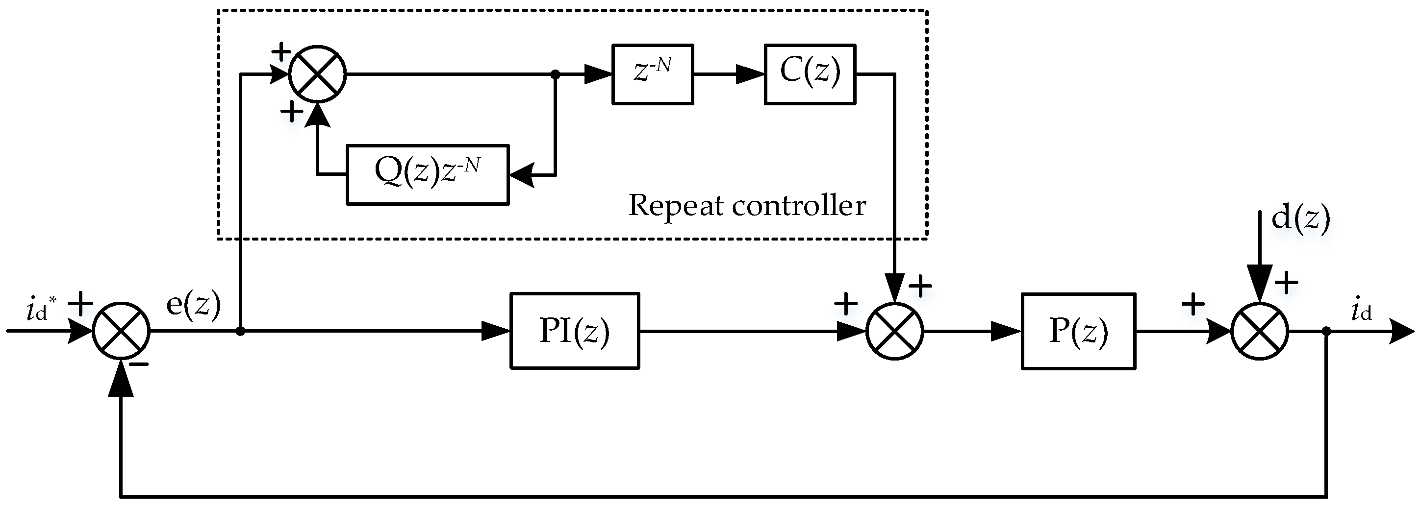
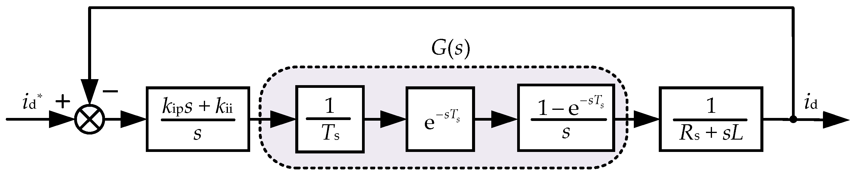
4.1. Front-Stage Three-Phase PFC Circuit Current Inner Loop Compound Controller

Figure 8 shows the design of the current inner loop compound controller with the d-axis as the analysis object. id* is the d-axis reference of the AC side current, id is the d-axis output of the AC side current, e(z) is the error between id* and id, C(z) is the compensator, P(z) is the transfer function of the discretized controlled object, d(z) is the disturbance signal, and PI(z) is the discretized PI regulator. When the d(z) is ignored, the error e(z) is acted by the PI regulator and repetitive controller together, and the generated control signal acts on the controlled object P(z).

4.1.1. Design of Repetitive Controller

Repetitive control is a new control method based on the internal model principle, which can effectively restrain periodic disturbance error. In the three-phase PFC circuit, due to the influence of the power tube dead zone time, periodic errors of the power grid current will occur, thus increasing the harmonic component of the power grid current. For periodic errors in the three-phase PFC circuit, although the PI controller will compensate and adjust, the effect is not ideal [20].
The transfer function of the repetitive controller is expressed as:
H ( z ) = z N · C ( z ) 1 Q ( z ) z N ,
where Q(z) = 0.97; N is the sampling times of one cycle; and C(z) is the compensator.
The transfer function of compensator C(z) is expressed as:
C ( z ) = k r z k ,
where kr is the amplitude compensation coefficient; and zk is the phase compensation link.
kr has a greater influence on the error convergence rate, and the value range of kr is 0 < k ≤ l. The larger the value, the faster the error convergence, so kr is taken as 1.
According to Equations (23) and (24), the transfer function of the repetitive controller can be obtained by:
H ( z ) = z N + k 1 Q ( z ) z N .

4.1.2. Design of Current Inner Loop PI Controller

After feedforward decoupling, the d-axis and q-axis components are independent of each other. Since the current inner loop adopts digital control, its sampling and calculation process will have a time-delay effect. Figure 9 shows the control system of the current inner loop, where esTs is the calculation delay link, (1 − esTs)/s is the zero-order hold link, and 1/(Rs + sL) is the controlled object of the current inner loop.
The transfer function G(s) of the digital controller consisting of the calculation delay link and the zero-order hold link is expressed as:
G ( s ) = 1 T s e s T s 1 e s T s s e 1.5 s T s 1 1 + 1.5 s T s ,
The current inner loop transfer function Goi(s) can be expressed as:
G oi ( s ) = k ii ( A s + 1 ) R s s ( 1 + 1.5 s T s ) ( 1 + s L R s ) ,
where L is the filter inductance; Rs is the parasitic resistance of filter inductor; and A = kip/kii is the parameter ratio of the current inner loop PI regulator.
According to the classic control theory, the zero point of the PI regulator is introduced into the current inner loop gain to offset the complex poles in the system, making the system a type I system [21]. When A = L/Rs, the expression of current inner loop transfer function Goi(s) can be simplified as:
G oi ( s ) = k ii R s s ( 1 + 1.5 s T s ) ,
Using the setting method of the second-order system, and taking the damping coefficient ζ = 0.707, then:
{ ω n 2 = k ii 1.5 R s T s 2 ζ ω n = 1 1.5 T s ,
where ωn is the undamped oscillation frequency; ζ is the damping coefficient; and Ts is the sampling time of the current inner loop.
Through calculation, the closed-loop transfer function Gci(s) of the current inner loop can be expressed as:
G ci ( s ) = G oi ( s ) 1 + G oi ( s ) 1 1 + 6 s T s .

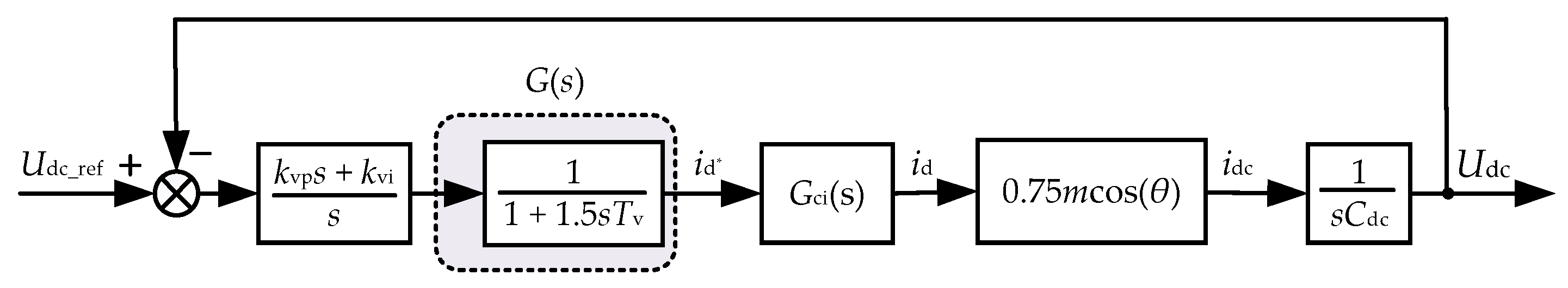
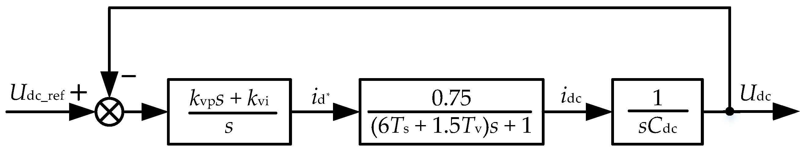
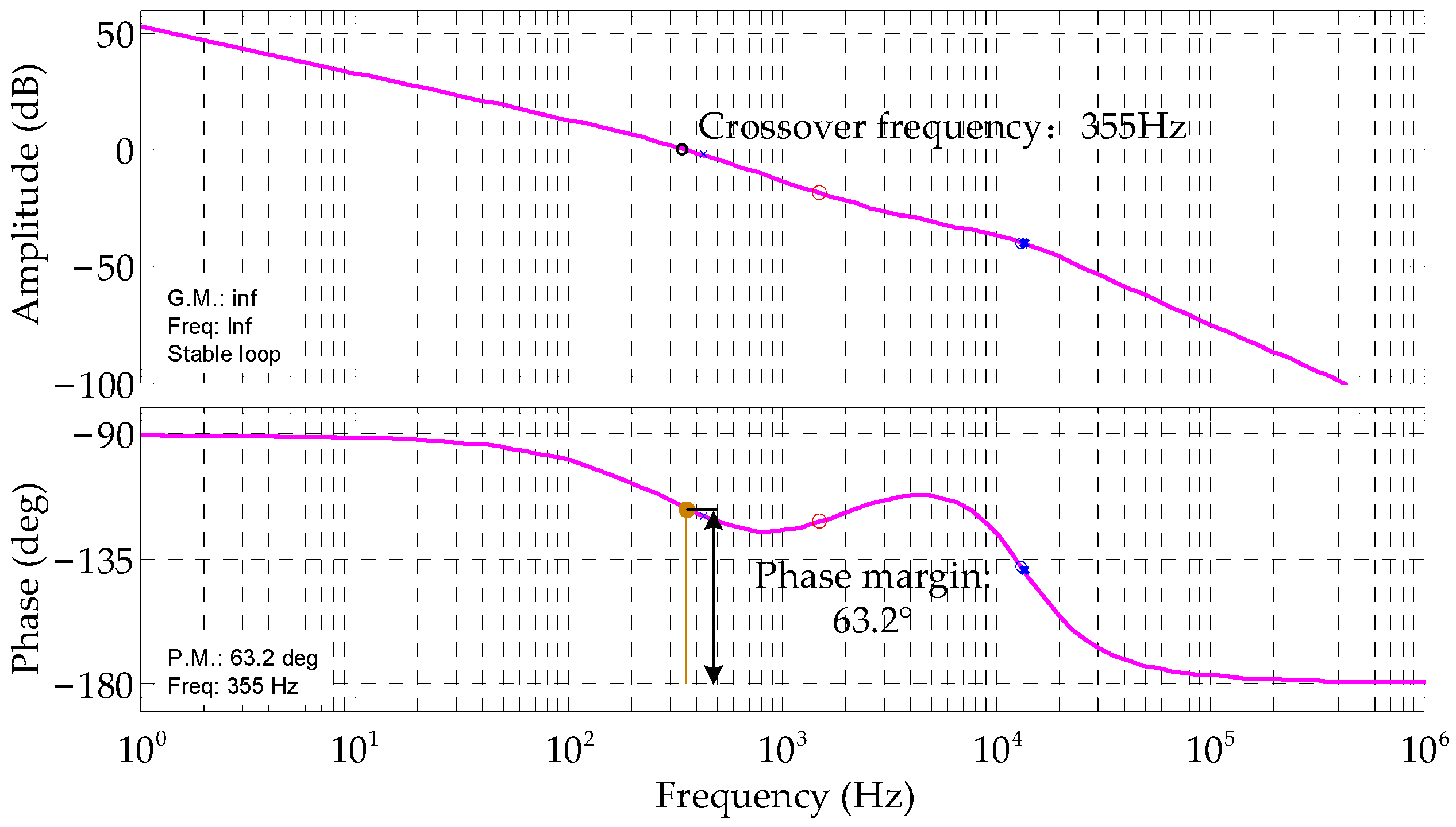
4.2. Front-Stage Three-Phase PFC Circuit Voltage Outer Loop Controller

The output current of the DC bus can be expressed as:
i dc = 0.75 i d m cos ( θ ) ,
where m is the modulation coefficient of the pre-stage PFC circuit; and θ is the initial phase angle of the switching function.
Figure 10 is the voltage outer loop control block diagram, where Gci(s) is the closed-loop transfer function of the current inner loop, kvp and kvi are the parameters of the voltage outer loop PI regulator, Tv is the sampling time of the front-stage output voltage, and 1/sCdc is the controlled object of the voltage outer loop.
Figure 11 is the simplified voltage outer loop control block diagram, combining the time constant 1.5 Tv of the digital controller in the voltage outer loop with the time constant 6 Ts in Gci(s) to simplify the voltage outer loop control system.
The voltage outer loop transfer function Gov(s) can be expressed as:
G ov ( s ) = 0.75 k vi ( k vp k vi s + 1 ) s 2 C dc [ ( 6 T s + 1.5 T v ) s + 1 ] ,
Let ω1 = kvi/kvp and ω2 = 1/(6 Ts + 1.5 Tv), then the frequency width of the voltage outer loop h is expressed as:
h = ω 2 ω 1 = k vp k vi ( 6 T s + 1.5 T v ) ,
According to the parameter design of a typical type II system [22], Equation (34) can be obtained:
0.75 k vi C dc = 1 h h ( 6 T s + 1.5 T v ) 2 ,
where Tv = 1 ms and the sampling time of the current inner loop Ts = 0.1 ms.
According to Equations (33) and (34), the parameters of the voltage outer loop PI regulator kvp and kvi are:
{ k vi = C dc 330.75 × h h T s 2 k vp = C dc 15.75 × h T s .

4.3. Control Strategy of Rear-Stage Full-Bridge LLC Resonant Converter

Since the LLC resonant converter contains a variety of working modes, a corresponding state-space model is established by using the piecewise linear space method, and nonlinear terms in system equations are linearly approximated by using the extended description function method [23]. The transfer function expression from switching frequency to the output voltage of the full-bridge LLC resonant converter is obtained as follows:
G vf ( s ) = K vf ( s C o r c + 1 ) ( s C o R L + 1 ) ( s 2 f s 2 + s f s Q e + 1 ) ,
where fs is the operating frequency of the full-bridge LLC resonant converter, fs = 85 kHz; Qe is the quality factor of the resonant converter; Co is the output holding capacitance; RL is the equivalent output load; and rc is the series equivalent resistance of the holding capacitance, rc  0.4 Ω.
K vf = u dc n [ f r 3 f s ( 1 + 1 L n f r L n f s ) 2 π L n f r 2 f s 3 [ ( 1 + 1 L n f r L n f s ) + Q e 2 ( f s f r f r f s ) 2 ] 3 2 + L n Q e 2 ( f s 2 f r 2 ) ( f s 2 + f r 2 ) 2 π L n f r 2 f s 3 [ ( 1 + 1 L n f r L n f s ) + Q e 2 ( f s f r f r f s ) 2 ] 3 2 ] ,
Equation (37) is simplified to obtain Kvf = 7.77 × 10⁻⁵.
According to Equations (36) and (37), the transfer function from the switching frequency to the output voltage of the LLC resonant converter can be expressed as:
G vf ( s ) = 7.77 × 1 0 5 ( 1.2 × 10 5 s + 1 ) ( 5.29 × 1 0 - 4 s + 1 ) ( s 2 7.23 × 1 0 9 + s 6.03 × 1 0 4 + 1 ) ,
According to Equation (38), the Bode diagram of the transfer function without adding the voltage PI controller is obtained, as shown in Figure 12.
Since the LLC resonant converter before correction is a 0-type system, it is necessary to add a PI controller to improve the system type, so that the mid-frequency band of the system drops at a slope of −20 dB/dec and crosses the 0 dB line, thereby improving the phase margin of the system and ensuring that the system has good stability.
In the constant voltage charging mode, the control block diagram of the LLC resonant converter after adding the voltage PI controller is shown in Figure 13.
The voltage outer loop PI controller can be expressed as:
P I v ( s ) = 3.62 × 10 7 ( 1 + 1.1 × 10 4 s ) s ,
In the constant voltage charging mode, the transfer function of the LLC resonant converter with the voltage PI controller is expressed as:
φ LL C v ( s ) = P I v ( s ) G vf ( s ) ,
From Equation (40), the system transfer function of the voltage PI controller is obtained, and the Bode diagram is shown in Figure 14.
It can be seen from Figure 14 that the LLC resonant converter has a crossing frequency of 355 Hz and a phase margin of 63.2°, which can meet the requirements of the stable regulation of the system and has a relatively stable middle frequency bandwidth. When the LLC resonant converter works in constant voltage mode, the working frequency of the primary side FET has a small variation range, and its output voltage range is 280–420 V. The transfer function of the LLC resonant converter has a small change, which is conducive to the design of a single-loop controller.

5. System Simulation Analysis

The circuit was simulated and analyzed in MATLAB/Simulink to examine the correctness and feasibility of the proposed single-phase and three-phase compatible isolated OBC and the control effect of the improved control strategy under the three-phase input condition. Figure 15 shows the main circuit model and control model built in the simulation software. The simulation parameters of the OBC are shown in Table 2.

5.1. Single-Phase Input Mode Simulation Waveform

(1)
Grid current waveform
Figure 16 shows the waveform of the power grid voltage and current under the single-phase input condition. It can be seen from the figure that the sine characteristic of the power grid current is good, the frequency and phase of power grid voltage are the same, and the circuit has a high-power factor. Figure 17 shows the power factor value, which is 0.997, and the correction effect is ideal.
(2)
Output voltage waveform
Figure 18 shows the output waveform of DC bus voltage Udc-s. After 0.1 s, the voltage is stable at about 400 V. The control effect is good and meets the design requirements. By amplifying the waveform of the labeled part, the peak-to-peak value of the voltage ripple is about 14 V, which is less than the ripple rate requirement of 5%.
Figure 19 shows the output waveform of the front-stage output voltage Udc. The voltage reaches stability after rapidly rising to 700 V and the overshot is small. The voltage ripple peak in the amplification area is about 1 V, which is far less than the ripple rate requirement, indicating that the front-stage circuit meets the design requirements under the single-phase working mode.

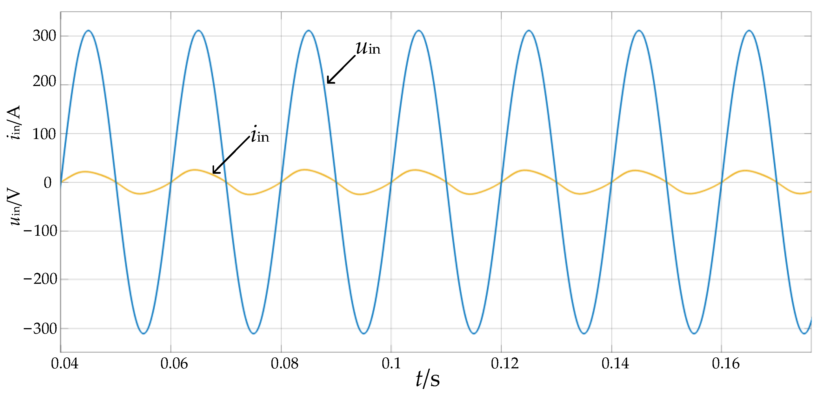
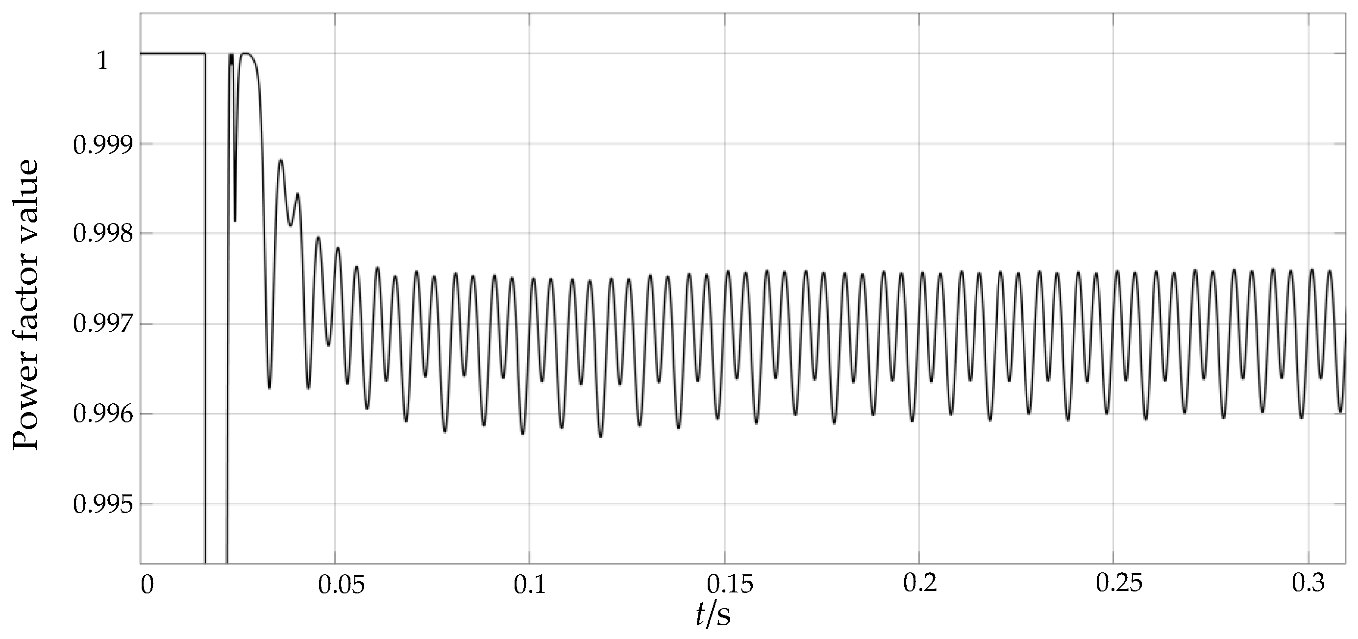
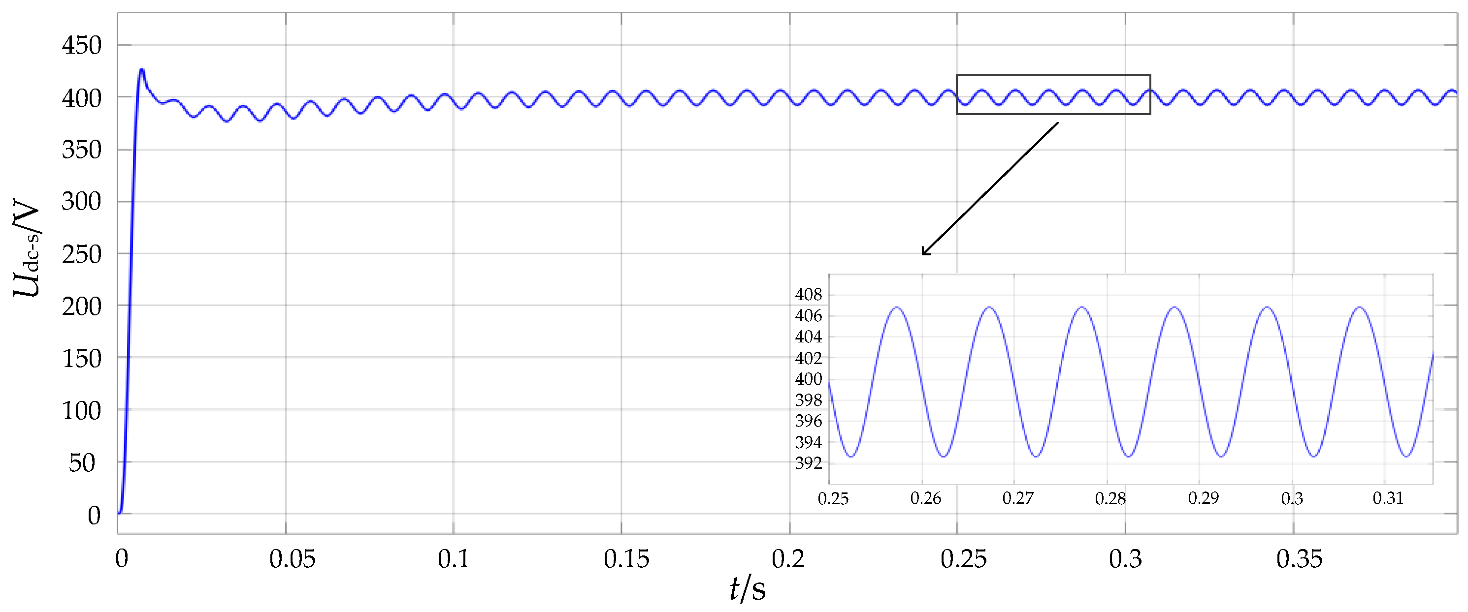
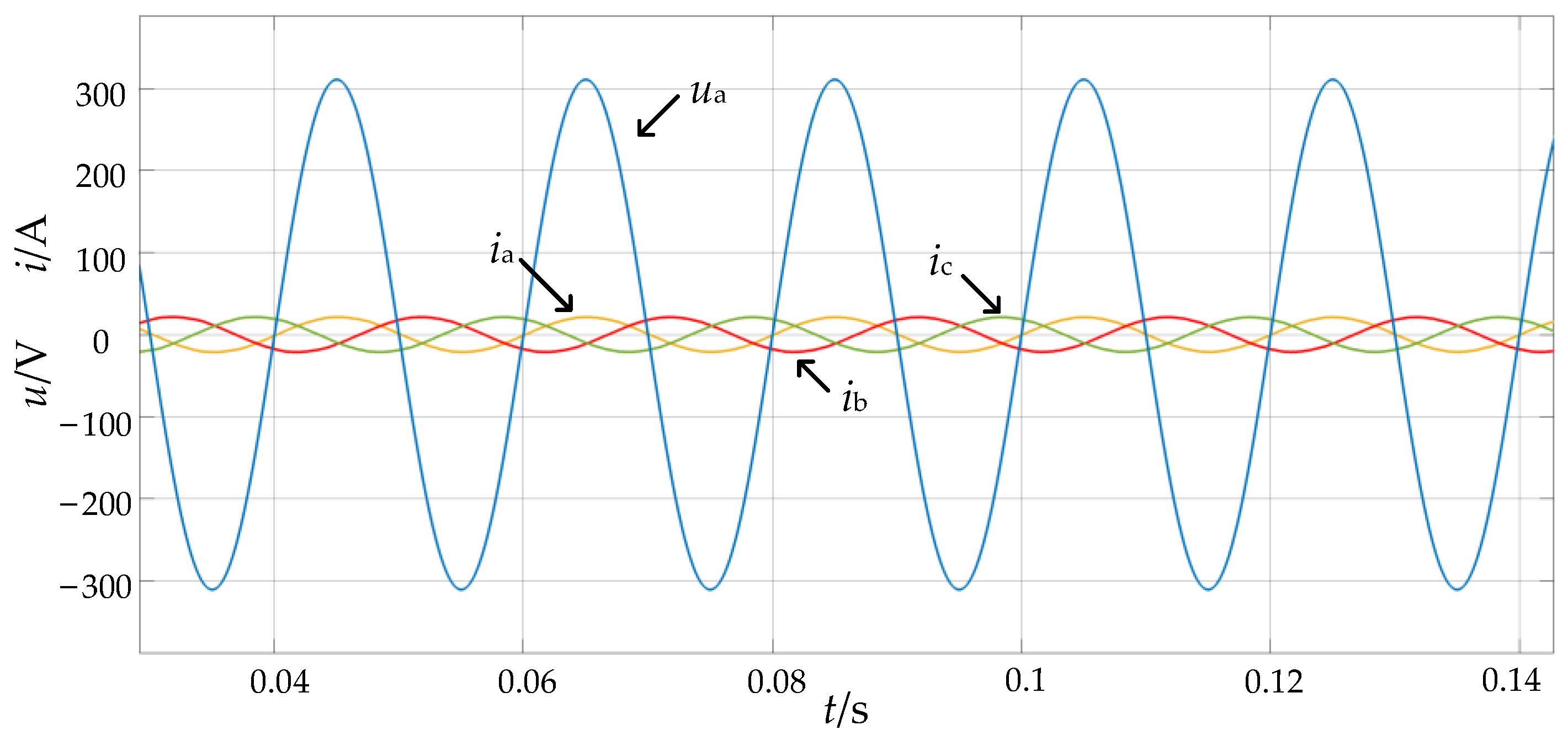
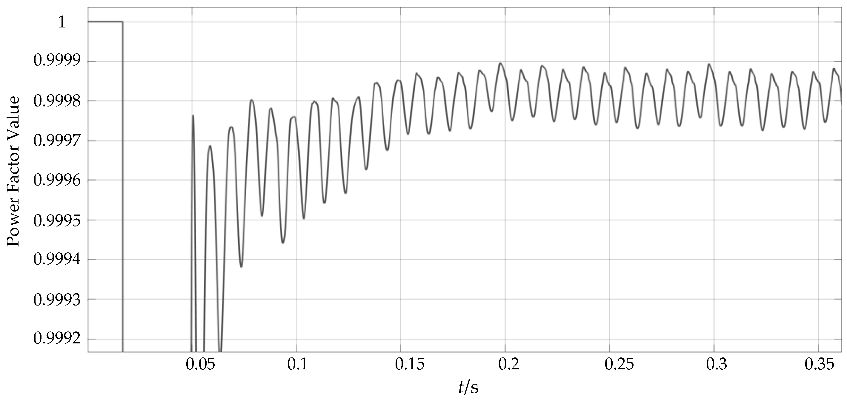
5.2. Three-Phase Input Mode Simulation Waveform
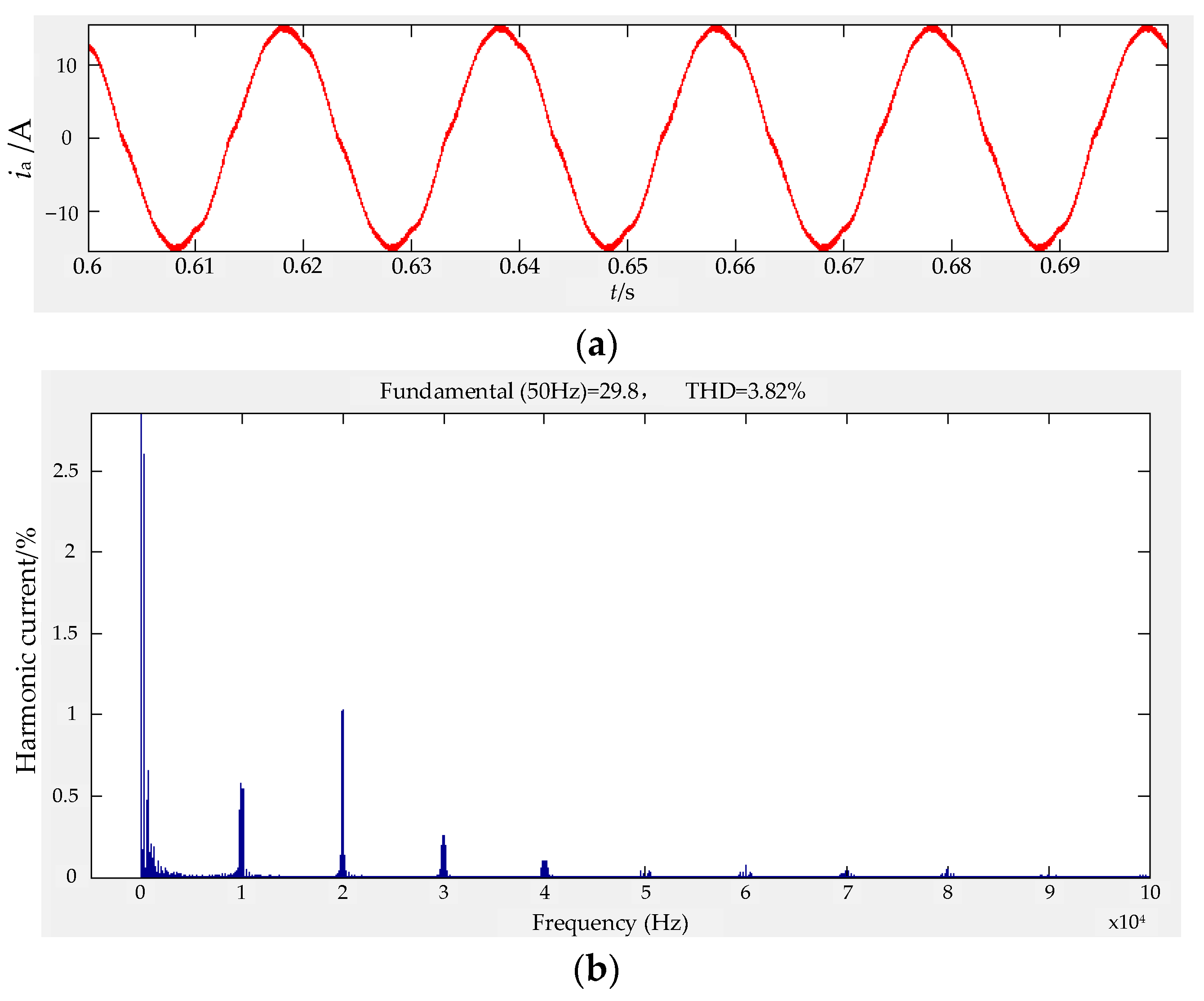
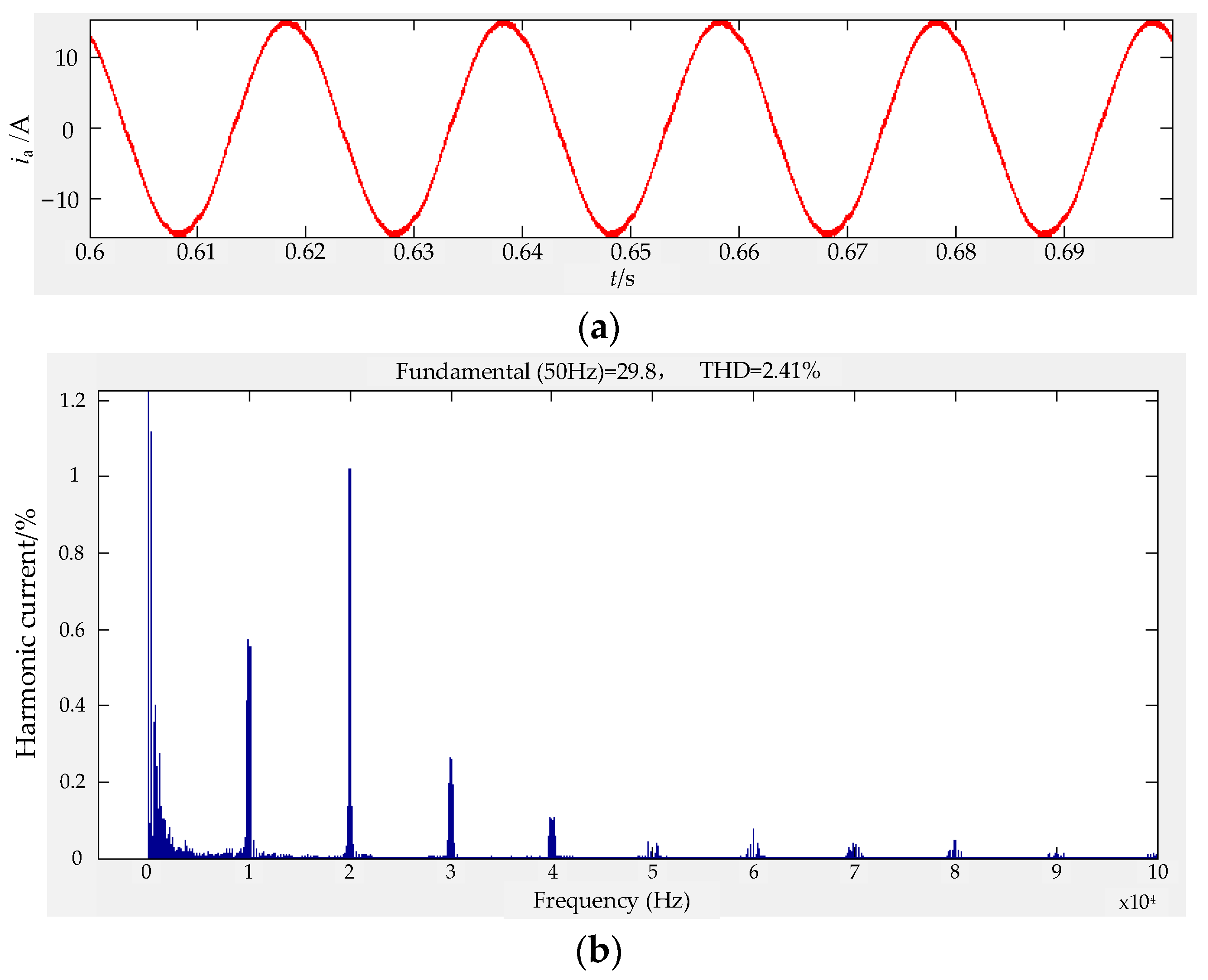
(1)
Power grid current wave type
As shown in Table 3, under the condition that all parameters are the same, the THD of the input current is compared between current inner loop PI control and current inner loop parallel PI-repetitive control under full load, half load, and 25% load, respectively.
It can be seen from Table 3 that under different load conditions, the input current THD with parallel PI-repeat control is always lower than that with PI control. Taking the full load case as an example, the input current waveform and the THD analysis figures of current inner loop with PI control and parallel PI-repetitive control are shown in Figure 20 and Figure 21, respectively. By comparing Figure 20a and Figure 21a, it can be seen that after the controller of current inner loop is improved, the waveform of input current is smoother. Compared with Figure 20b and Figure 21b, it can be seen that the THD of the current inner loop parallel PI-repetitive control is significantly reduced, indicating that the repetitive control has a better inhibition effect on the periodic error.
Figure 22 shows the waveform of the power grid voltage and current under the three-phase input condition. In the steady-state operation, the three-phase input current is a smooth sine wave shape after compound control, and the current distortion is small. The phase of a-phase input current is always consistent with the phase of input voltage. Figure 23 shows the power factor value. It can be seen from the figure that the circuit works in a state of high-power factor, and the power factor value is higher than 0.99, which meets the expected setting requirements.
(2)
Output voltage waveform
Figure 24 shows the output bus voltage waveform of the three-phase PFC circuit. After about 0.1 s, the system enters a steady state, and the bus voltage follows the given voltage value, and the overshoot is small. At the same time, the ripple value of the voltage is about 0.2 V, which is far less than the ripple rate of 5% and meets the design expectation.

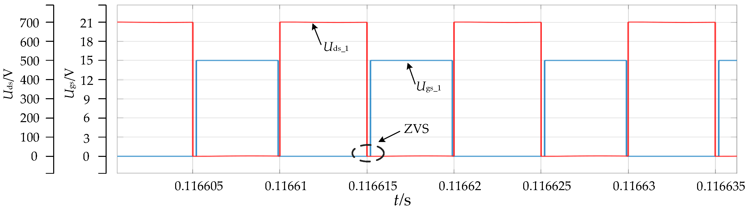
5.3. Simulation Waveform of Rear-Stage Full-Bridge LLC Resonant Converter

Figure 25 shows the driving waveform of the FET of the LLC resonant converter when the charger is working. Ugs-1 is the driving signal of Q1 and Q3, and Ugs-2 is the driving signal of Q2 and Q4. On the same bridge arm, the driving signals of two sets of FETs are complementary and have dead time. Figure 26 shows the waveforms of the drain-source voltage and the driving voltage of the MOSFET. After the drain-source voltage Uds_1 of the MOSFET drops to zero, the corresponding driving voltage Ugs_1 begins to rise, and the primary side MOSFET realizes zero voltage switching (ZVS).
Figure 27 shows the waveform of the resonant capacitance voltage UCr, resonant current ILr, and the central point voltage Uab of the original side when no load. At this point, the resonant current appears as a triangular wave shape. When the voltage at the central point of the primary side falls, the resonant current is greater than zero, indicating that the primary side FETs have ZVS characteristics.
Figure 28 shows the waveform of the resonant capacitance voltage UCr, resonant current ILr, and the central point voltage Uab of the original side at full load. When the switching frequency of the LLC resonant converter is equal to the resonant frequency, the waveform of the resonant current is approximately sine wave. When the voltage at the central point of the primary side falls, the resonant current is greater than zero, and the resonant cavity presents sensibility, and the primary side FETs can realize ZVS.
Figure 29 shows the rated output voltage waveform of the LLC resonant converter at full load. At about 0.02 s, the output voltage can reach a stable value of 350 V. When 50% load jump is set at 0.3 s, the output voltage will have a small fluctuation, which can be restored to a stable value after about 0.08 s.

6. Conclusions

This paper proposes a two-stage isolated OBC that can be compatible with single-phase and three-phase AC voltage inputs. By switching the relay on and off, the front stage can realize the switching of single-phase and three-phase PFC circuits. The rear-stage circuit is the full-bridge LLC resonant converter. When the single-phase voltage input, the front stage circuit is the totem pole PFC circuit cascade boost circuit; When the three-phase voltage input, the front stage circuit is the three-phase six-switch PFC circuit. The control strategy of the three-phase PFC circuit is optimized, and a repetitive controller is introduced into the current inner loop to reduce the harmonic distortion rate of input current. By designing and calculating the parameters of the OBC, the effectiveness of the proposed circuit structure and control strategy is verified in simulation software. The simulation results show that the vehicle charger can realize the single-phase and three-phase AC voltage input and realize the PFC function, the DC output voltage level of the front stage is the same under the two working conditions. At the same time, the rear-stage LLC resonant converter can realize soft switching in the full load range. After the repetitive controller is introduced into the current inner loop of the three-phase PFC circuit, the waveform of input current is improved, and the THD of input current is lower than that of current inner loop PI control under different load conditions, which has a good control effect.

Author Contributions

Conceptualization, K.Z.; methodology, K.Z., S.-M.C., N.-Z.J. and D.-Y.S.; software, S.-M.C.; supervision, K.Z., N.-Z.J. and D.-Y.S.; writing—review and editing, S.-M.C. All authors have read and agreed to the published version of the manuscript.

Funding

This research was supported by Heilongjiang Provincial Natural Science Foundation of China, grant number LH2021E086.

Institutional Review Board Statement

Not applicable.

Informed Consent Statement

Not applicable.

Data Availability Statement

Not applicable.

Conflicts of Interest

The authors declare no conflict of interest. The funders had no role in the design of the study; in the collection, analyses, or interpretation of data; in the writing of the manuscript, or in the decision to publish the results.

References

  1. Alireza, K.; Michael, D. Global trends in high-power on-board chargers for electric vehicle. IEEE Trans. Veh. Technol. 2019, 68, 3306–3324. [Google Scholar]
  2. Andreas, T.; Peter, B.A.; Tim, U.; Chresten, T.; Mattia, M. Electrification of personal vehicle travels in cities-Quantifying the public charging demand. eTransportation 2021, 9, 100125. [Google Scholar]
  3. Mi, N.; Sasic, B.; Marshall, J.; Tomasiewicz, S. A novel economical single stage battery charger with power factor correction. In Proceedings of the 18th Annual IEEE Applied Power Electronics Conference and Exposition, Miami, FL, USA, 9–13 February 2003. [Google Scholar]
  4. Zhao, W.H.; Shen, Y.X. Review on the research of electric vehicle on-board charger topologies. Control Eng. China 2019, 26, 29–36. [Google Scholar]
  5. Dai, H.C.; Ye, X.T.; Shou, Y.L.; Wang, Z.S. Research on control strategy of on-board charger (OBC) based on PFC and LLC two-level structure. Electr. Eng. 2020, 11, 38–42. [Google Scholar]
  6. Park, M.-H.; Baek, J.; Jeong, Y.; Moon, G.-W. An interleaved totem-pole bridgeless boost PFC converter with soft-switching capability adopting phase-shifting control. IEEE Trans. Power Electron. 2019, 34, 10610–10618. [Google Scholar] [CrossRef]
  7. Shi, C.; Wang, H.Y.; Dusmez, S.; Khaligh, A. A SiC-based high-efficiency isolated onboard PEV charger with ultrawide DC-link voltage range. IEEE Trans. Ind. Appl. 2017, 53, 501–511. [Google Scholar] [CrossRef]
  8. Meng, T.; Ben, H.Q.; Wang, X.S. A passive flyback auxiliary circuit with integrated transformer suitable for three-phase isolated full-bridge boost PFC converter. IEEE Trans. Power Electron. 2016, 31, 4995–5003. [Google Scholar] [CrossRef]
  9. Ebrahimi, S.; Taghavi, M.; Tahami, F.; Oraee, H. Integrated bidirectional isolated soft-switched battery charger for vehicle-to-grid technology using 4-Switch 3Φ-rectifier. In Proceedings of the IECON 39th Annual Conference of the IEEE Industrial Electronics Society, Vienna, Austria, 10–13 November 2013. [Google Scholar]
  10. Kim, H.; Park, J.; Kim, S.; Hakim, R.M.; Belkamel, H.; Choi, S. A single-stage electrolytic capacitor-less EV charger with single- and three-phase compatibility. IEEE Trans. Power Electron. 2022, 37, 6780–6791. [Google Scholar] [CrossRef]
  11. Zhang, T.S.; Peng, Y.Q.; Zhao, Y.Y.; Huang, X.R.; Liu, X.R. Research on double closed loop interval Type II fuzzy control model of front-stage variable on-board charger. Control Eng. China, 2022; 1–13, early access. [Google Scholar] [CrossRef]
  12. Zhou, S.Y. Research on Single and Three-Phase Compatible VIENNA Rectifier. Master’s Thesis, Nanjing University of Aeronautics and Astronautics, Nanjing, China, 2020. [Google Scholar]
  13. Sadilek, T.; Jang, Y.; Hao, S.; Jia, M.; Barbosa, P.; Husain, I. A new PFC CCM boost rectifier with extended gain and reduced voltage switching for 1-ph/3-ph universal input on-board charger for electric vehicles. In Proceedings of the 5th IEEE Applied Power Electronics Conference and Exposition, Phoenix, AZ, USA, 14–17 June 2021. [Google Scholar]
  14. Cao, J.F.; Xiong, H.J.; Lei, D.M. LCL-type grid-connected inverter based on fractional-order PID control. In Proceedings of the 3rd International Conference on Industrial Informatics-Computing Technology, Intelligent Technology, Industrial Information Integration (ICIICII), Wuhan, China, 2–3 December 2017. [Google Scholar]
  15. Liu, B.; Ben, H.; Bai, Y.; Sun, S. Analysis and suppression of current harmonics in grid side of PWM rectifiers during light load. Trans. China Electrotech. Soc. 2017, 31, 162–168. [Google Scholar]
  16. Ali, M.; Wang, L.; Chen, G. Design and control aspect of segmented proportional integral-repetitive controller parameter optimization of the three-phase boost power factor correction rectifier. Int. J. Circuit Theory Appl. 2021, 49, 554–575. [Google Scholar] [CrossRef]
  17. Zhang, J.; Wang, J.; Zhang, G.; Qian, Z. A hybrid driving scheme for full-bridge synchronous rectifier in LLC resonant converter. IEEE Trans. Power Electron. 2012, 27, 4549–4561. [Google Scholar] [CrossRef]
  18. Deng, J.; Li, S.; Hu, S.; Mi, C.; Ma, R. Design methodology of LLC resonant converters for electric vehicle battery Chargers. IEEE Trans. Veh. Technol. 2014, 63, 1581–1592. [Google Scholar] [CrossRef]
  19. Zhang, Z.G.; Li, S.F.; Li, X.; Cheng, P.M.; Luo, Q.M. A high efficiency totem-pole bridgeless PFC converter in CCM mode. Proc. CSEE 2022, 42, 1957–1968. [Google Scholar]
  20. He, L.; Zhang, K.; Xiong, J. A repetitive control scheme for harmonic suppression of circulating current in modular multilevel converters. IEEE Trans. Power Electron. 2015, 30, 471–481. [Google Scholar] [CrossRef]
  21. Zhou, K.; Fang, H.L.; Liu, Y. Driving–charging integrated controller for electric vehicles. IEEE Access 2022, 10, 66545–66563. [Google Scholar] [CrossRef]
  22. Yang, Y.; Zhang, J. Phase compensation resonant control strategy for three-phase PWM converter. Electr. Mach. Control 2013, 17, 43–49. [Google Scholar]
  23. Zhou, K.; Yuan, C.X.; Sun, D.Y.; Jin, N.Z.; Wu, X.G. Parameter adaptive terminal sliding mode control for Full-Bridge DC-DC converter. PLoS ONE 2021, 16, e0247228. [Google Scholar] [CrossRef] [PubMed]
Figure 1. Single-phase and three-phase compatible isolated on-board charger (OBC).
Energies 15 06445 g001
Figure 2. Three-phase working mode.
Energies 15 06445 g002
Figure 3. Single-phase working mode.
Energies 15 06445 g003
Figure 4. Equivalent circuit of LLC resonant converter.
Energies 15 06445 g004
Figure 5. Normalized voltage gain curve.
Energies 15 06445 g005
Figure 6. Single-phase working mode control strategy.
Energies 15 06445 g006
Figure 7. Three-phase working mode control strategy.
Energies 15 06445 g007
Figure 8. Current inner loop composite control block diagram.
Energies 15 06445 g008
Figure 9. Current inner loop control block diagram.
Energies 15 06445 g009
Figure 10. Control block diagram of voltage outer loop.
Energies 15 06445 g010
Figure 11. Simplified voltage outer loop control block diagram.
Energies 15 06445 g011
Figure 12. Bode diagram of transfer function without voltage PI controller.
Energies 15 06445 g012
Figure 13. Control block diagram of adding voltage PI controller.
Energies 15 06445 g013
Figure 14. Bode diagram of transfer function with voltage PI controller.
Energies 15 06445 g014
Figure 15. Simulation model of OBC.
Energies 15 06445 g015
Figure 16. Power grid voltage and current waveform (single-phase input).
Energies 15 06445 g016
Figure 17. Power factor (single-phase input).
Energies 15 06445 g017
Figure 18. DC bus voltage Udc-s.
Energies 15 06445 g018
Figure 19. Front-stage output voltage Udc.
Energies 15 06445 g019
Figure 20. Current inner loop with PI control. (a) the waveform of the input current; (b) the THD analysis of the input current.
Energies 15 06445 g020
Figure 21. Current inner loop with parallel PI-repetitive control. (a) the waveform of the input current; (b) the THD analysis of the input current.
Energies 15 06445 g021
Figure 22. Power grid voltage and current waveform (three-phase input).
Energies 15 06445 g022
Figure 23. Power factor (three-phase input).
Energies 15 06445 g023
Figure 24. Output bus voltage.
Energies 15 06445 g024
Figure 25. FET driving waveform.
Energies 15 06445 g025
Figure 26. FET drain-source voltage and driving voltage waveform.
Energies 15 06445 g026
Figure 27. Voltage waveform of the resonant capacitance, resonant current, and the voltage waveform at the center point of the original side of LLC at no-load condition.
Energies 15 06445 g027
Figure 28. Voltage waveform of the resonant capacitance, resonant current, and the voltage waveform at the center point of the primary side of LLC at full-load condition.
Energies 15 06445 g028
Figure 29. Waveform of rated output voltage.
Energies 15 06445 g029
Table 1. Main performance indicators of on-board charger (OBC).
Performance IndicatorValue
Input phase voltage range (Uin)176~264 V
Input voltage frequency range (f)45~65 Hz
DC bus voltage (Udc-s)400 V
Front-stage output voltage (Udc)700 V
Output voltage range (Uo)280~420 V
Rated output voltage (Uo_nor)350 V
PFC circuit switching frequency (fsw)50 kHz
Power factor≥0.99
Efficiency (η)≥93%
Table 2. The OBC simulation parameters.
Simulation ParameterValue
Filter inductance (L)1 mH
DC bus capacitance (Cdc-s)2700 μF
DC bus capacitance (Cdc)2000 μF
Resonant inductance (Lr)68 μH
Resonant capacitance (Cr)37.25 nF
Excitation inductance (Lm)170 μH
Output holding capacitance (Co)4000 μF
Table 3. Under different load conditions, the THD of the input current obtained by PI control and PI-repetitive control.
LoadCurrent Inner Loop PI ControlCurrent Inner Loop PI-Repetitive Control
THD (%)THD (%)
Full Load3.822.41
Half Load6.744.36
25% Load10.828.65
Publisher’s Note: MDPI stays neutral with regard to jurisdictional claims in published maps and institutional affiliations.

