Article

Minimum-Output-Current-Ripple Control of Current-Fed Three-Level Phase-Shift Full-Bridge Converter

National Key Laboratory of Science and Technology on Vessel Integrated Power System, Naval University of Engineering, Wuhan 430033, China
*
Author to whom correspondence should be addressed.
Energies 2022, 15(17), 6444; https://doi.org/10.3390/en15176444
Submission received: 28 July 2022 / Revised: 31 August 2022 / Accepted: 31 August 2022 / Published: 3 September 2022
(This article belongs to the Section F: Electrical Engineering)

Abstract

:
Electrified ports using medium-voltage DC (MVDC) renewable energy microgrids require current-fed dc/dc converters in application scenarios such as battery or ultracapacitor charging units and hydrogen production systems. This paper designs a three-level phase-shift full-bridge (TL-PSFB) converter that interfaces with the MVDC microgrid. Its operation in the current source mode requires a wide output voltage range and small output current ripple. Firstly, the dual-output TL-PSFB topology is introduced, and the principle of phase-shift pulse width modulation (PS-PWM) is presented. Secondly, the principle of the traditional constant-conduction-duty-cycle (CCDC) strategy is analyzed. Then, a minimum-output-current-ripple (MOCR) strategy is proposed by analyzing the relationship between output current ripple, conducting-duty cycle, and phase-shift duty cycle, and a constant current control combined with the MOCR strategy is designed. The output current ripple of the MOCR strategy is smaller than that of the CCDC strategy in a full range of operating conditions. Under the same output current ripple design index, the value and loss of the filter inductor can be reduced with the MOCR strategy. In addition, the MOCR strategy can widen the output voltage regulation range and increase the bus voltage utilization without causing significant changes to the total harmonic distortion (THD) of primary voltage. Finally, experimental results verify the correctness of the theoretical analysis.

1. Introduction

Inland and offshore shipping is facing an energy transition due to the economic and environmental concerns of fossil fuels. Currently, there are some new energy vessels [1] and electrified port projects applied [2]. Compared with the port microgrid directly supplied by the power grid, the addition of renewable energy can significantly reduce the utilization rate of fossil fuel. Port microgrids using renewable energy generation have immediate environmental benefits as well as long-term economic benefits. Due to the large randomness of power supply and load of renewable energy microgrid, the AC microgrid is prone to frequency fluctuation and grid oscillation problems. As a new form of network formation, a medium-voltage DC (MVDC) microgrid can avoid the above problems and has the advantages of high reliability of power supply, fast response, and scalability. The typical structure of an MVDC renewable energy microgrid is shown in Figure 1.
The wind power generation, photovoltaic power generation, and hydroelectric power generation on the source side of the renewable energy microgrid, and the charging device on the load side all have strong intermittensity. The connection of the source side to the public network can solve the short-term high power demand of the load, while the hydrogen production system on the load side can effectively solve the local consumption of renewable energy generation and bring new energy types. Ships with different working scenarios can choose energy sources such as hydrogen fuel, battery, and ultracapacitor storage.
MVDC input dc/dc converters for load-side charging devices or hydrogen production power sources are important components of medium-voltage DC renewable energy microgrids. The common topologies include the non-isolated Buck converter and Boost converter, isolated series resonant converter, phase-shift full-bridge converter, and bidirectional full bridge converter, etc. In MVDC applications, series or multi-level connections are usually used on the basis of the above topologies to increase output voltage level. Switching device withstand voltage is half of the bus voltage in the three-level phase-shift full-bridge (TL-PSFB) topology which can meet the requirements of MVDC input [3,4]. The TL-PSFB topology adopts an intermediate frequency transformer to achieve isolation and voltage transformation, and can flexibly configure the output side voltage according to the power of the electrolyzer or the voltage of the energy storage device. Magnetic coupling can effectively isolate source and load faults.
Some scholars have performed much research on the TL-PSFB converter controlled in voltage mode. The TL-PSFB converter and the basic topological derivation are described by Prof. Xinbo Ruan in [4]. In [5], a three-phase TL-PSFB converter topology was designed with voltage mode control. Literature [6] proposes a first-order sliding mode controller, which can eliminate the output voltage error by adding an integrator and achieve a better control effect. The principle analysis, modeling, and control strategy of the voltage mode controlled TL-PSFB converter are studied in the literature mentioned above.
Higher power density and efficiency has always been the goal of the power electronic converter. Increasing the switching frequency of the power device is the most direct method, however, it will cause a sharp increase in the loss caused by hard switching of switching devices. Therefore, many scholars have been studying soft switching strategies, and the main methods can be divided into two categories: proposing a new modulation strategy and improving the topology structure. The new modulation strategies reported in the literature mainly include an asymmetric duty cycle modulation strategy [7], double phase-shift modulation strategy [8], and triple phase-shift modulation strategy [9], etc. These strategies can extend the soft-switching range of the converter to a certain extent without changing the topology or adding additional energy storage elements, but they cannot achieve soft-switching in the full operating range. In [10,11,12,13,14,15], LLC resonant TL-PSFB converter was studied to achieve a wider range of soft switching with the help of resonant element energy storage. Dr. Bor-Ren Lin designed a new hybrid topology, including a three-level half-bridge converter and unregulated voltage half-bridge converter structure, which has the advantages of small circulation, wide soft-switching range, and small output current ripple [16,17,18]. In addition, soft switching of the primary-side switching device can be achieved by adding a clamp diode [19] or fly-across capacitor to the primary side [20,21,22]. Prof. Yan Li’s focus is on the intermediate AC side. She proposed a hybrid TL-PSFB converter to accommodate a wide range of output voltages by adding a clamp inductor on the AC side, and the converter has good soft switching performance [23]. Soft switching of the secondary diode has also been noticed in the literature [24,25,26]. In addition, some scholars have done some improving research on the topology in some other aspects. Literature [27,28] proposed an improved modulation strategy to equalize the thermal stress of power devices or supporting capacitors. A modulation strategy to reduce the common-mode voltage was proposed in the literature [29]. In order to solve the reverse recovery problem of the secondary rectifying diode, the active clamping strategy was proposed in [30,31].
Only literature [19] (hundred kW class) and [5] (MW class) have publicly reported the application of TL-PSFB converter in large-capacity DC conversion applications. Large-capacity TL-PSFB converters have high losses and complex heat dissipation design. Traditional topology with improved modulation or control strategy do not fundamentally solve the problem of narrow soft-switching range and are prone to soft-switching failure. Resonant topology or other improved topology increases power loop components, has complex topology and low reliability, and the added devices also bring losses. Therefore, the soft switching strategy is not the focus of the design of a large capacity TL-PSFB converter.
Previous research has focused on the voltage-mode controlled TL-PSFB converter, while hydrogen power or energy storage converters require a current source, the major difference between them is that current mode control has no static operating point. In addition, the output current ripple of the converter directly affects the efficiency of the electrolyzer or energy storage system, which requires the converter to have a smaller output current ripple.
This paper is organized as follows. In Section 2, a dual-output TL-PSFB topology is proposed. The principle of phase-shift pulse width modulation (PS-PWM) is introduced, and the design method of the traditional CCDC strategy is analyzed. In Section 3, the relationship between output current ripple and conducting-duty cycle and phase-shift duty cycle is analytically calculated, and a constant current control with the MOCR strategy is proposed. Section 4 compares and analyzes the performance of the two strategies in terms of output current ripple, filter inductance parameters, DC voltage utilization, and the total harmonic distortion (THD) of primary voltage. In Section 5, the proposed modulation method’s effectiveness is verified by experiments. Finally, Section 6 summarizes the main work of this paper.

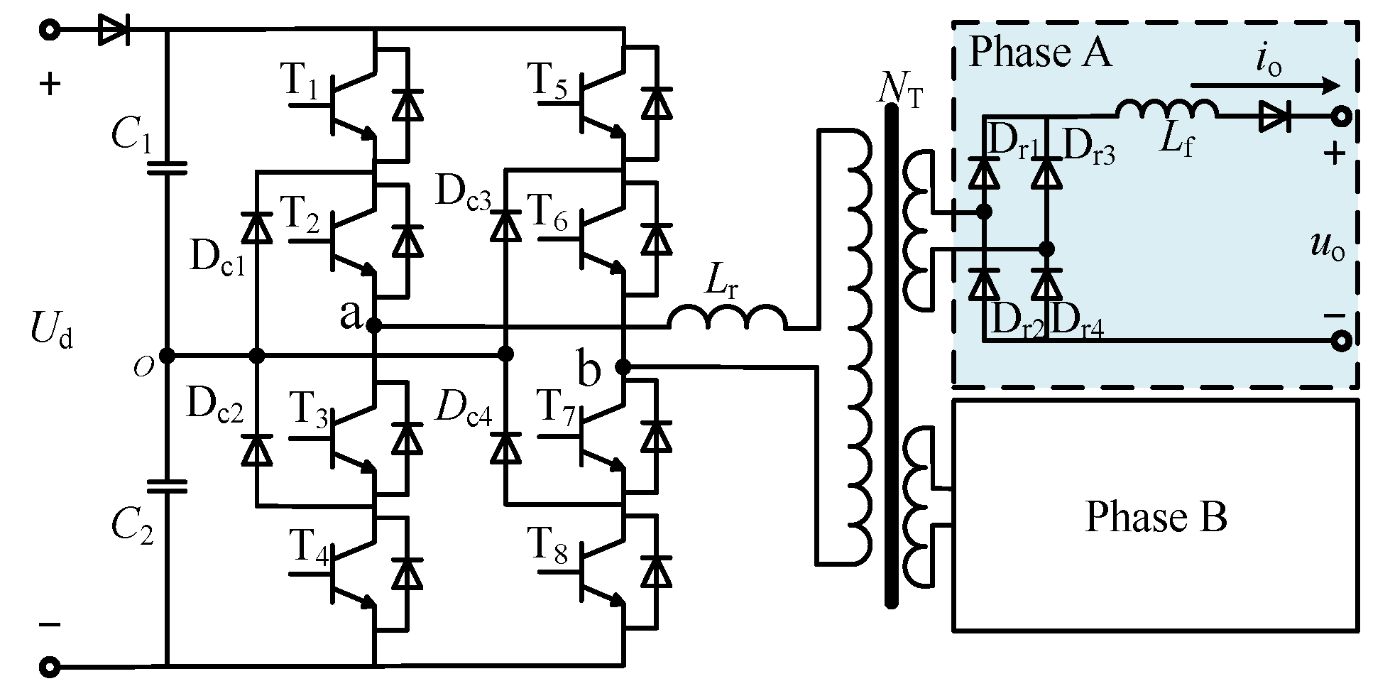
2. Principle of Dual-Output TL-PSFB Converter

2.1. Topology and Principle of PS-PWM
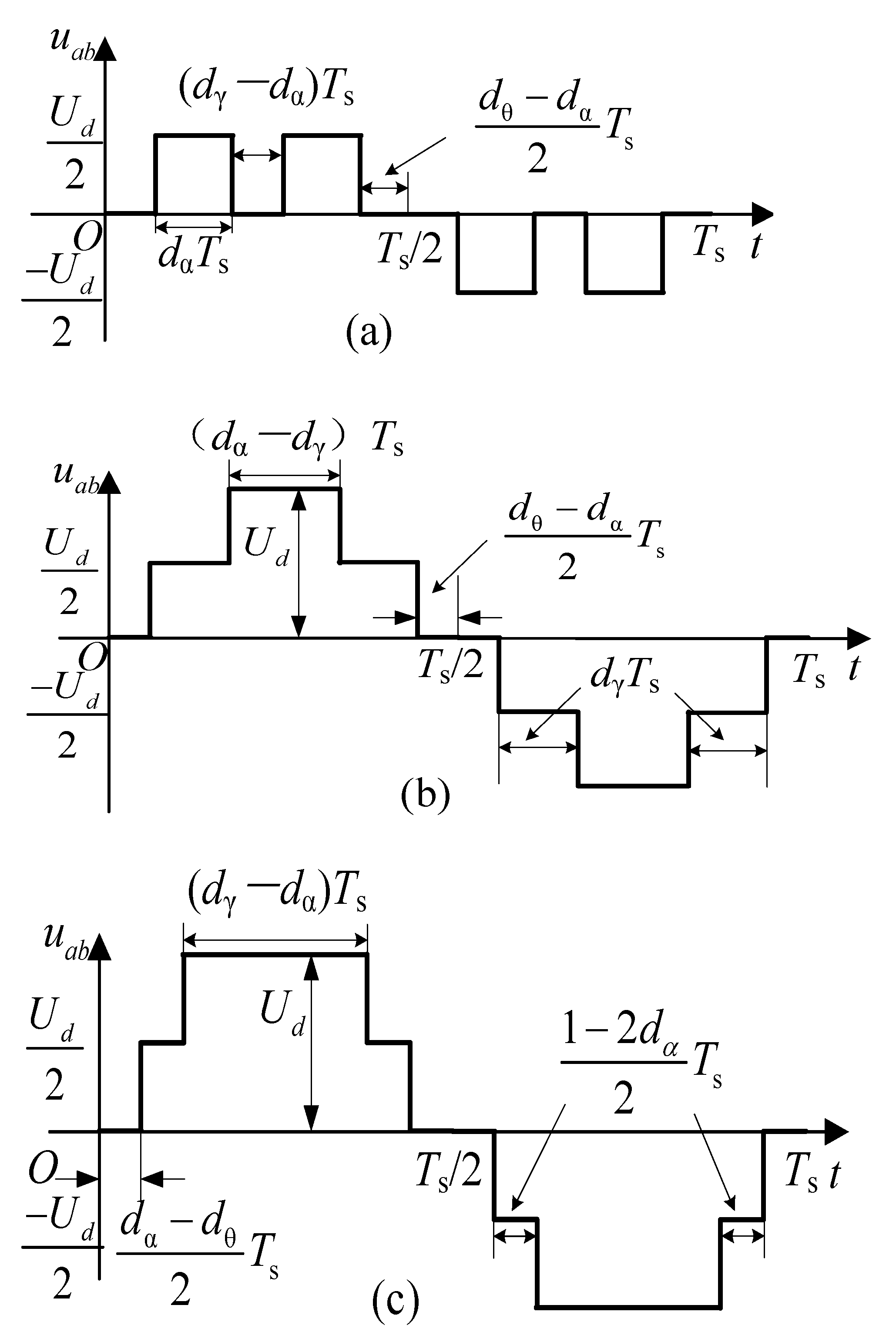
In order to improve the power density of the converter, a dual-output TL-PSFB converter topology is designed in this paper, as shown in Figure 2. The dual-output TL-PSFB converter mainly includes support capacitors, diode-clamped three-level H-bridge, three-winding medium-frequency transformer, uncontrolled rectifier bridge, output filter inductor, and input and output diodes. The diode-clamped three-level H-bridge inverter unit converts the input DC voltage into a bipolar five-level square wave with adjustable pulse width, which is divided into two output channels after the step-down by the three-winding medium-frequency transformer. Then it is connected to two independent sets of uncontrolled rectifier bridges. Only inductive filtering is used at the rectifier output, reducing unnecessary passive components compared to previous LC or LCL filters.
PS-PWM is adopted in the dual-output TL-PSFB converter, and its principle is shown in Figure 3. In the figure, dθ is the conducting-duty cycle, dα is the phase-shift duty cycle, and Ts is the switching period. The diode-clamped three-level H-bridge in Figure 2 uses the same dθ for the odd-numbered switching devices and a complementary conducting-duty cycle 1 − dθ for the even-numbered switching devices. The driving pulse of the right bridge leg lags behind that of the left bridge leg, and the phase difference of the driving pulse of the left and right bridge legs’ switches is changed by controlling the carrier delay time of the right bridge leg dαTs. PS-PWM consists of two degrees of freedom: dθ and dα, both in the range of [0, 1/2].
By analyzing the corresponding relationship between dθ and dα, the output voltage of the diode-clamped three-level H-bridge can be obtained, including the three cases as shown in Figure 4. In order to distinguish different conditions of output voltages more clearly, the clamping duty cycle dγ is introduced, where dγ = 1/2 − dθ.

2.2. CCDC Strategy

The design principle of the CCDC strategy is to minimize THD of the primary voltage uab. The root mean square (RMS) of the nth harmonic component of uab is noted as Unrms (n = 1, 2, 3…). THD of uab is defined as,
THD = 1 U 1 rms ( n = 2 U n rms 2 ) 1 / 2
where the relationship between the rms value Urms of uab and the rms value of each harmonic component is,
U rms 2 = n = 1 U n rms 2
as known from the calculation,
THD = 1 U 1 rms ( U rms 2 U 1 rms 2 ) 1 / 2
According to the waveform of uab in Figure 4, the Fourier series expression of uab can be obtained by analytical calculation shown in (4).
u a b ( t ) = n = 1 ( b n sin n t ) , b n = 8 U d n T s sin n d θ π sin n d α π ( n = 1 , 3 , 5 , 7 )
In addition, the relationship between the RMS value of uab, dθ and dα is shown in (5).
U rms = { U d d α 0 < d α d γ U d 2 d α + d θ 1 2 d γ < d α d θ U d d α + 2 d θ 1 2 d θ < d α 1 2
Combining (4) and (5) with (2) and (3), THD of uab can be obtained as shown in (6).
THD = { 2 π 2 d α 16 sin 2 π d θ sin 2 π d α 1 0 < d α d γ π ( 4 π d α 1 / 2 + 2 π d θ ) 16 sin 2 π d θ sin 2 π d α 1 d γ < d α d θ π ( 2 π d α 1 / 2 + 4 π d θ ) 16 sin 2 π d θ sin 2 π d α 1 d θ < d α 1 2
Partial differential solution of (6) is performed; that is, let ∂THD/∂dα = 0 and ∂THD/∂dθ = 0, it can be obtained,
{ 4 π d α 1 2 + 2 π d θ = 2 tan π d α d γ < d α d θ 2 π d α 1 2 + 4 π d θ = tan π d α d θ < d α 1 2
{ 4 π d α 1 2 + 2 π d θ = tan π d θ d γ < d α d θ 2 π d α 1 2 + 4 π d θ = 2 tan π d θ d θ < d α 1 2
Two sets of solutions can be obtained by combining (7) and (8) as follows: the first extremum point is: dθ1 = 0.42, dα1 = 0.35; the second one is: dθ2 = 0.35 and dα2 = 0.42, which are the two extreme points shown in Figure 5.
The primary voltage is input to the uncontrolled rectifier bridge via the medium-frequency transformer. Similarly, the Fourier decomposition of the rectifier bridge output voltage ur is performed according to the relative relationship between dθ and dα.
u r = { 2 U d d α N T + n = 1 4 U d n T s N T cos 2 π n d θ sin 2 π n d α cos n ω t 0 < d α d γ 2 U d d α N T + n = 1 4 U d n T s N T cos 2 π n d θ sin 2 π n d α cos n ω t 0 < d α d γ 2 U d d θ N T + n = 1 4 U d n T s N T sin 2 π n d θ cos 2 π n d α cos n ω t d θ < d α 1 2
According to (9), the maximum DC component of the output voltage of the rectifier bridge is determined by dθ, and the output voltage can be regulated within the range of the maximum DC component by adjusting dα under the condition that dθ remains unchanged.
The dθ of the CCDC strategy is fixed at one of the two minimum points in Figure 5, and the upper limit of the DC component of the output voltage of the rectifier bridge is determined by dθ according to (9). In order to improve the utilization of the DC voltage at the primary side and obtain a wider regulation range, the CCDC strategy is usually set dθ = 0.42 and dα = 0.35.

3. MOCR Strategy

In this section, the output current ripple of the converter is analytically calculated, and the variation trend of the output current ripple with dθ and dα is analyzed. Then, a MOCR strategy is proposed, and a constant current control with the MOCR strategy is designed.

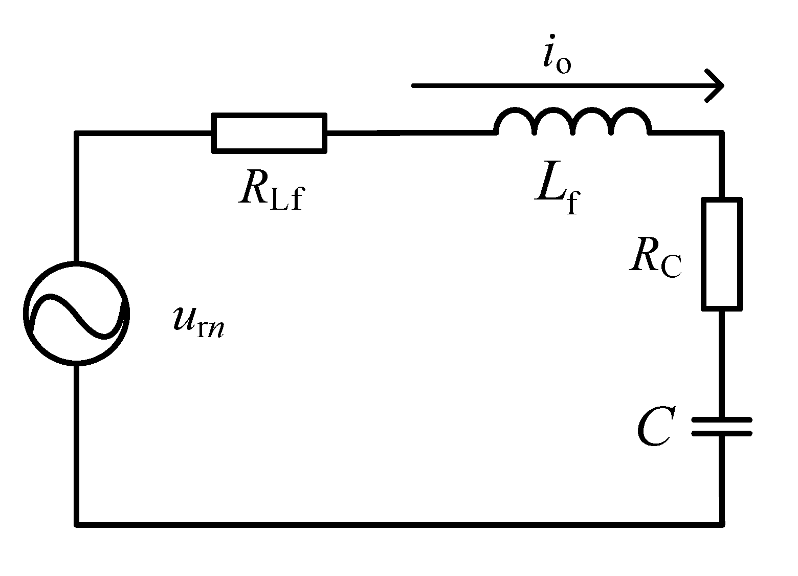
3.1. Analysis of Output Voltage and Current Ripple of the Rectifier Bridge

According to (9), the output voltage of the rectifier bridge is a DC component superimposed several times of AC harmonic components, so the DC component of the output voltage can be ignored when analyzing the harmonics of the filter inductor, and the load side can be equivalent to a series of resistor and capacitor. Different loads (such as ultracapacitors, batteries, electrolyzers, etc.) affect the RC parameters. The equivalent circuit at the output end of the rectifier bridge is shown in Figure 6.
Transform the AC harmonic component of the output voltage of the rectifier bridge obtained by (9) into a complex domain expression,
U · r n = { n = 1 2 2 U d n T s N T cos 2 π n d θ sin 2 π n d α 0 0 < d α d γ n = 1 2 2 U d n T s N T cos 2 π n d θ sin 2 π n d α 0 d γ < d α d θ n = 1 2 2 U d n T s N T sin 2 π n d θ cos 2 π n d α 0 d θ < d α 1 2
The harmonic component of the output current is,
I o n · = U · r n R C   +   R Lf   +   j n ω L f   +   1 j n ω C = U · r n R C   +   R Lf   +   j n 2 ω 2 L f C     1 n ω C
Substitute (10) into (11) to obtain,
I · o n = { n = 1 2 2 U d n T s N T cos 2 π n d θ sin 2 π n d α Re ( Z ) ϕ 0 < d α d γ n = 1 2 2 U d n T s N T cos 2 π n d θ sin 2 π n d α Re ( Z ) ϕ d γ < d α d θ n = 1 2 2 U d n T s N T sin 2 π n d θ cos 2 π n d α Re ( Z ) ϕ d θ < d α 1 2
where,
Re ( Z ) = ( R C + R L ) 2 + ( n 2 ω 2 L f C     1 n ω C ) 2 ϕ = arctan [ n 2 ω 2 L f C     1 n ω C ( R C   +   R L ) ]
Express the output current harmonics into the form in the real number field as
i o n = { n = 1 2 2 U d n T s N T cos 2 π n d θ sin 2 π n d α Re ( Z ) cos ( n ω t ϕ ) 0 < d α d γ n = 1 2 2 U d n T s N T cos 2 π n d θ sin 2 π n d α Re ( Z ) cos ( n ω t ϕ ) d γ < d α d θ n = 1 2 2 U d n T s N T sin 2 π n d θ cos 2 π n d α Re ( Z ) cos ( n ω t ϕ ) d θ < d α 1 2
Figure 7 shows the comparison between the calculated waveforms and the simulated waveforms for the output currents at different dθ and dα, the trend of the calculated results is generally consistent with that of the simulation results, which proves the correctness of the calculated results. There is a certain error between the calculated and simulated results, which is mainly due to the fact that the calculated results do not take into account non-ideal factors such as duty cycle loss.
The output current ripple is equal to the maximum value of the filter inductor current minus the minimum value in one cycle.
i o = max ( i o ) T s min ( i o ) T s
Combining (14) and (15), the variation of output current ripple under different combinations of dθ and dα can be calculated, as shown in Figure 8 and Figure 9.

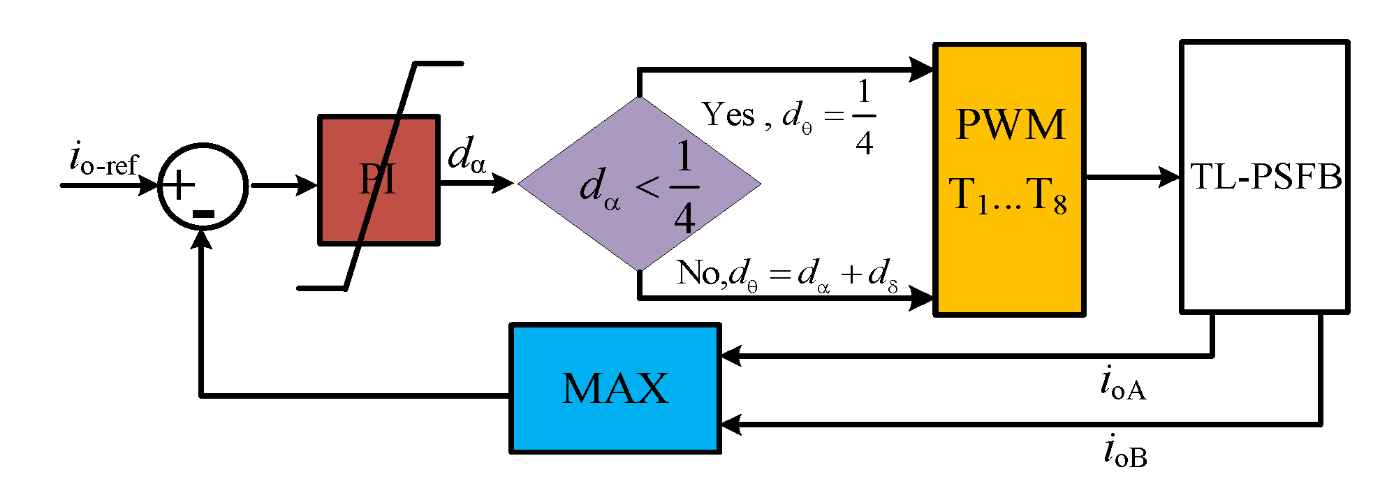
3.2. Constant Current Control Combined with the MOCR Strategy

As can be seen from Figure 9, as dθ and dα increase, there is a changing path that minimizes the output current ripple. That is,
{ d α , d θ 1 4 { d α = 1 4 ; d θ = 0 1 4 : RouteI d θ = 1 4 ; d α = 0 1 4 : RouteII 1 4 < d α , d θ 1 2 d α = d θ = 1 4 1 2 : RouteIII
Equation (16) is the mathematical description of the minimum output current ripple control rate. Since dθ determines the upper limit of the output voltage, transition path Route II→Route III is selected to ensure that the control variable is unique. That is, when dθ is less than 1/4, maintain dθ = 1/4 and adjust dα to control the output voltage. As the output voltage increases, control dθ is equal to dα.
Combined with the above analysis, this paper designs a constant current control combined with the MOCR strategy, as shown in Figure 10. The controller collects the output current for feedback, and dα is calculated by the PI controller, and dθ is calculated by the MOCR strategy. Since the converter adopts a secondary dual output structure, a two-output maximum current feedback strategy is used to prevent the output from being overloaded during actual operation. In Figure 10, dδ is limited to zero level, which is set to prevent the same level jump as the bus voltage. In engineering, the value is set according to the dv/dt limit of switching devices and transformers.

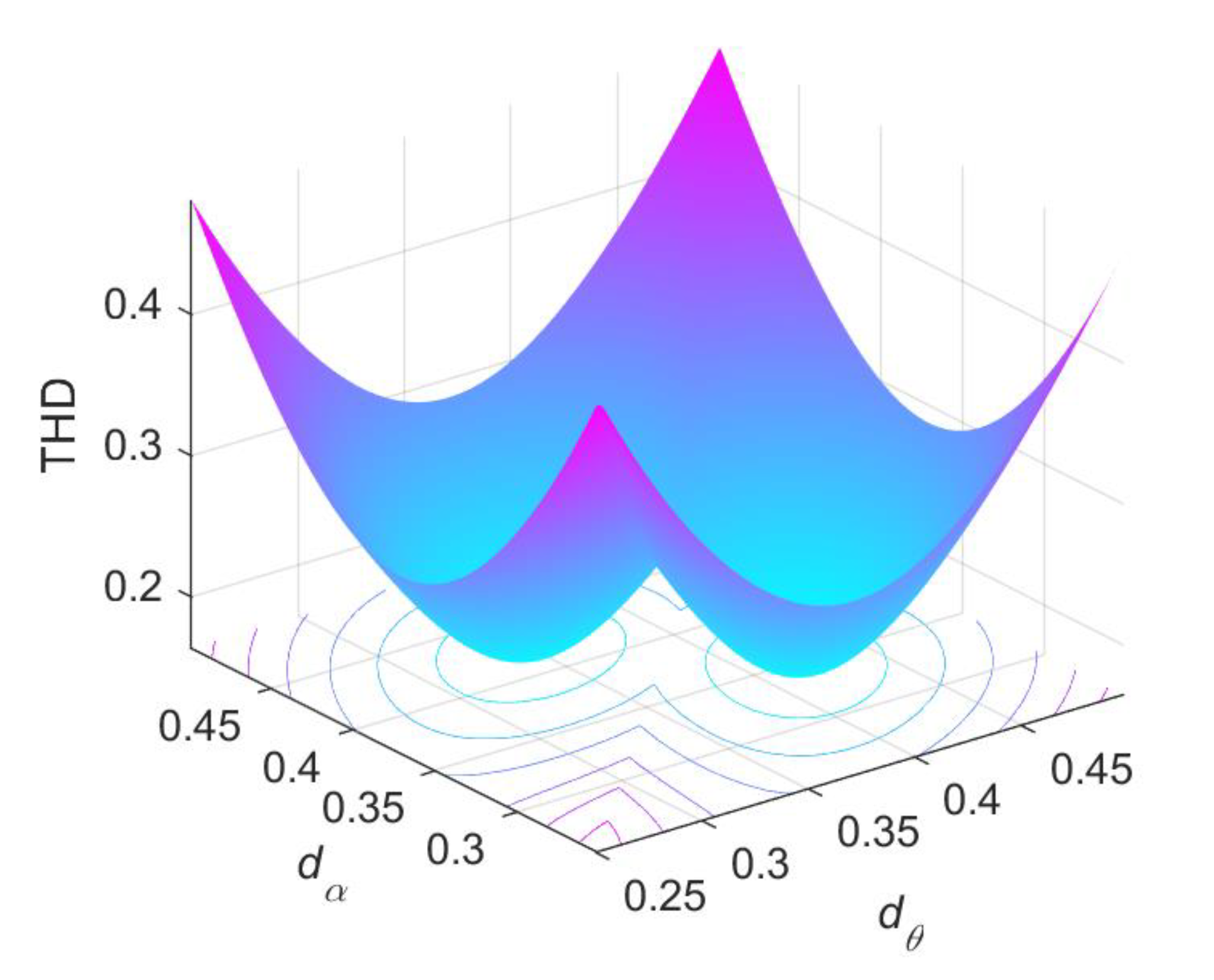
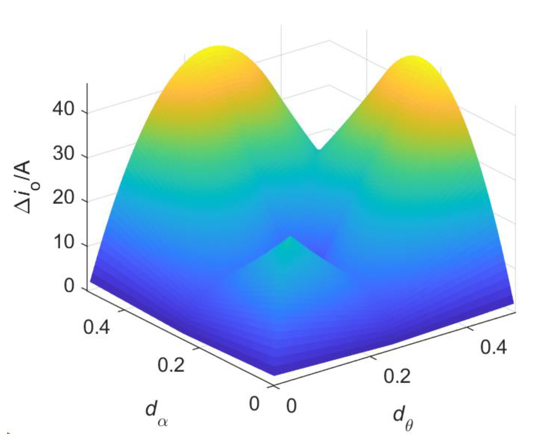
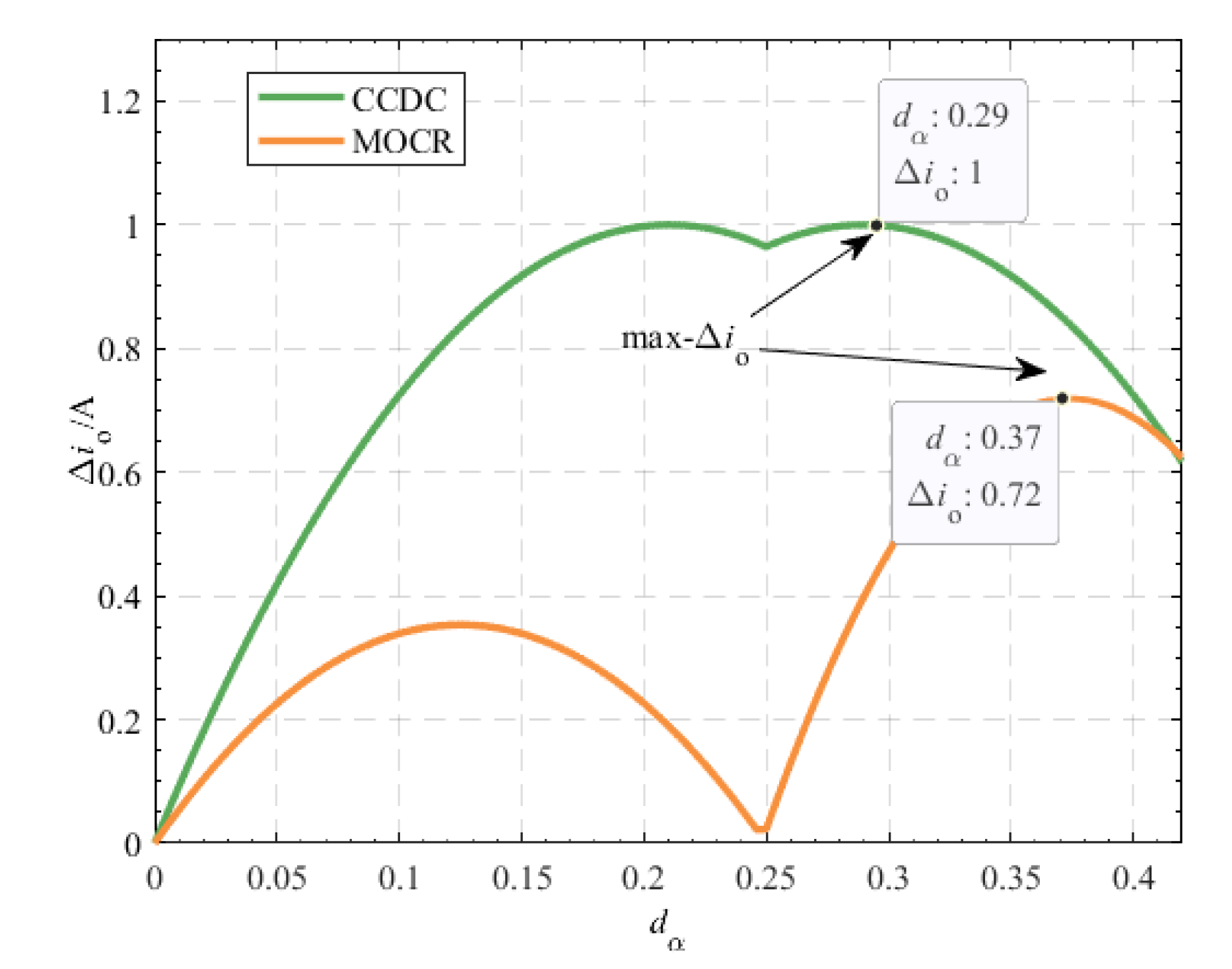
4. Comparison of CCDC and MOCR

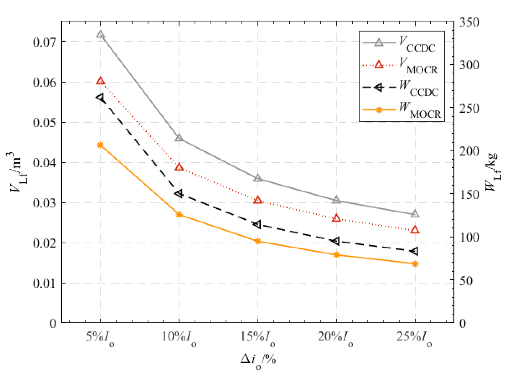
4.1. Output Current Ripple and Filter Inductor Characterization

Since dα can only be adjusted within the range less than dθ in the CCDC strategy, the output ripple of the two control strategies is compared below in the range [0, 0.42). Figure 11 shows the comparison of the normalized results of output current ripple under the same filtering inductance condition. It can be seen from the figure that the maximum ripple current modulated by the MOCR strategy is 28% smaller than that controlled by the traditional CCDC strategy, and the ripple current modulated by the MOCR strategy is all less than the CCDC strategy in the whole range of working conditions.
In Figure 11, dα corresponding to the maximum current ripple under the two strategies is obtained by the analytical calculation method, thus, the minimum filter inductance value satisfying the maximum ripple index can be calculated. Table 1 compares the values of minimum filter inductance corresponding to the two modulation methods under different output current ripple indexes. According to the data in the table, under different output current ripple indexes, the MOCR strategy can reduce the value of the minimum output filter inductance by about 23%.
According to the inductor multi-objective optimization design method studied in [32] and the parameters in Table 1, the output filter inductor is designed. Figure 12 shows the comparison of the volume and weight of the minimum inductance required by the two strategies corresponding to different output current ripple indexes. It can be seen from the figure that the volume and weight of the output filter inductor can be optimized to a certain extent by using the MOCR strategy studied in this paper under different requirements of ripple indexes, which will improve the power density of the converter.
The loss of filter inductor mainly includes core loss and winding loss. The winding losses can be decomposed into the sum of ac and dc losses,
L Cu = I o 2 R dc + n = 1 i o n 2 R ac n
where Rdc is the dc resistance of the filter inductor, and this parameter can be calculated from the average turn length and resistivity of the inductor winding. Rdc-n is the winding ac resistance corresponding to the ripple current of different frequencies. The relation between ac resistance and ac resistance is shown in (18). FR is the ac resistivity, which can be obtained by the Dowell model [33].
R ac n = F R R dc
Generally, core loss is calculated by loss separation theory and mainly includes hysteresis loss, eddy current loss, and other losses. According to the calculation formula of magnetic core loss derived in [32], combined with (17), the total loss of inductance can be calculated. Figure 13 shows a comparison of the output filter inductance loss with different parameters. It can be seen from the figure that, under the same output current ripple index requirements, the MOCR strategy can reduce the loss of output filtering inductor by up to 29.31%, which improves the efficiency of the converter to a certain extent.

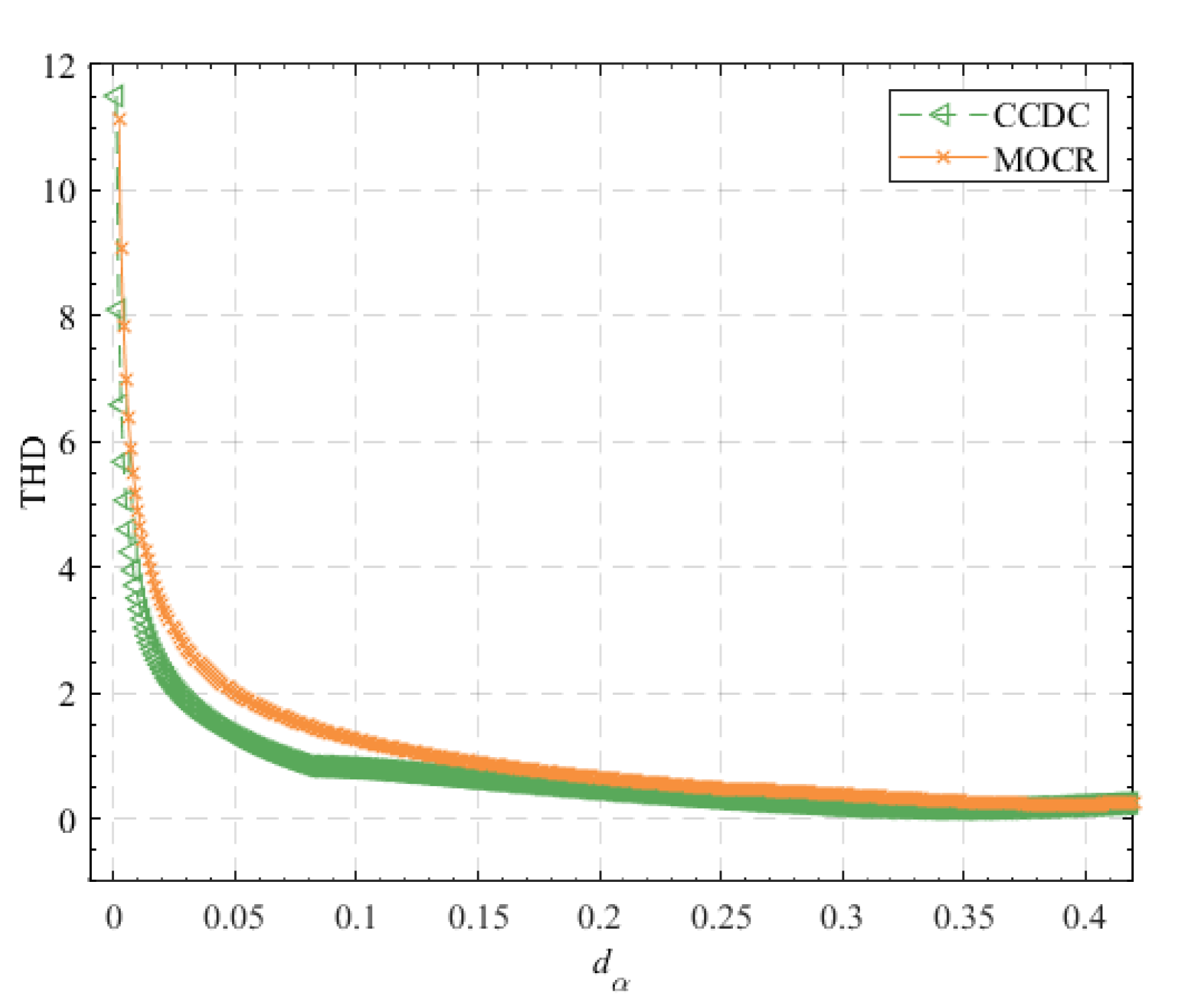
4.2. Utilization of DC Voltage and THD of Primary Voltage Characterization

The utilization of DC voltage is the ratio of the fundamental wave amplitude of uab to Ud. Combining with (4). The variation of DC voltage utilization with dθ and dα can be obtained by combining (4).
U ab U d = 8 T s sin d θ π sin d α π
The theoretical regulation range of both dθ and dα is [0, 0.5). A fixed dθ of 0.42 for the CCDC strategy leads to lower utilization of the primary-side DC voltage. This leads to a larger transformer ratio required to achieve the designed output voltage, which will increase the primary side current and, in turn, leads to an increased transformer and primary side switching device losses. Besides, the circuit parameters of the converter are designed according to the rated working condition in general. However, dα in the light load working condition is far away from 0.35, which will result in the increase of the THD of uab, as shown in Figure 14, which violates the initial design principle.
Figure 14 compares the THD of uab with the CCDC and MOCR strategies, respectively, over the full range of operating conditions, and it can be seen from the figure that the difference in THD performance between the two strategies under the corresponding operating conditions is not significant. However, it should be noted that the CCDC strategy is optimized for the THD of uab, but the optimization range is limited to the operating conditions around dθ of 0.42 and dα of 0.35. The CCDC strategy does not bring optimal performance for a wide range of output requirements.

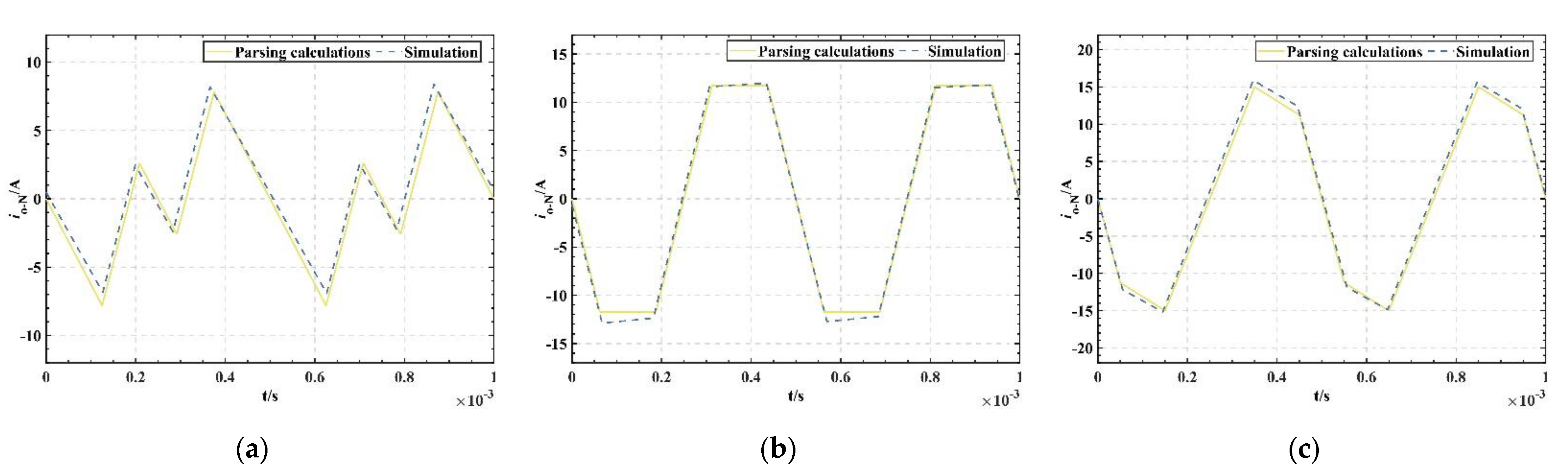
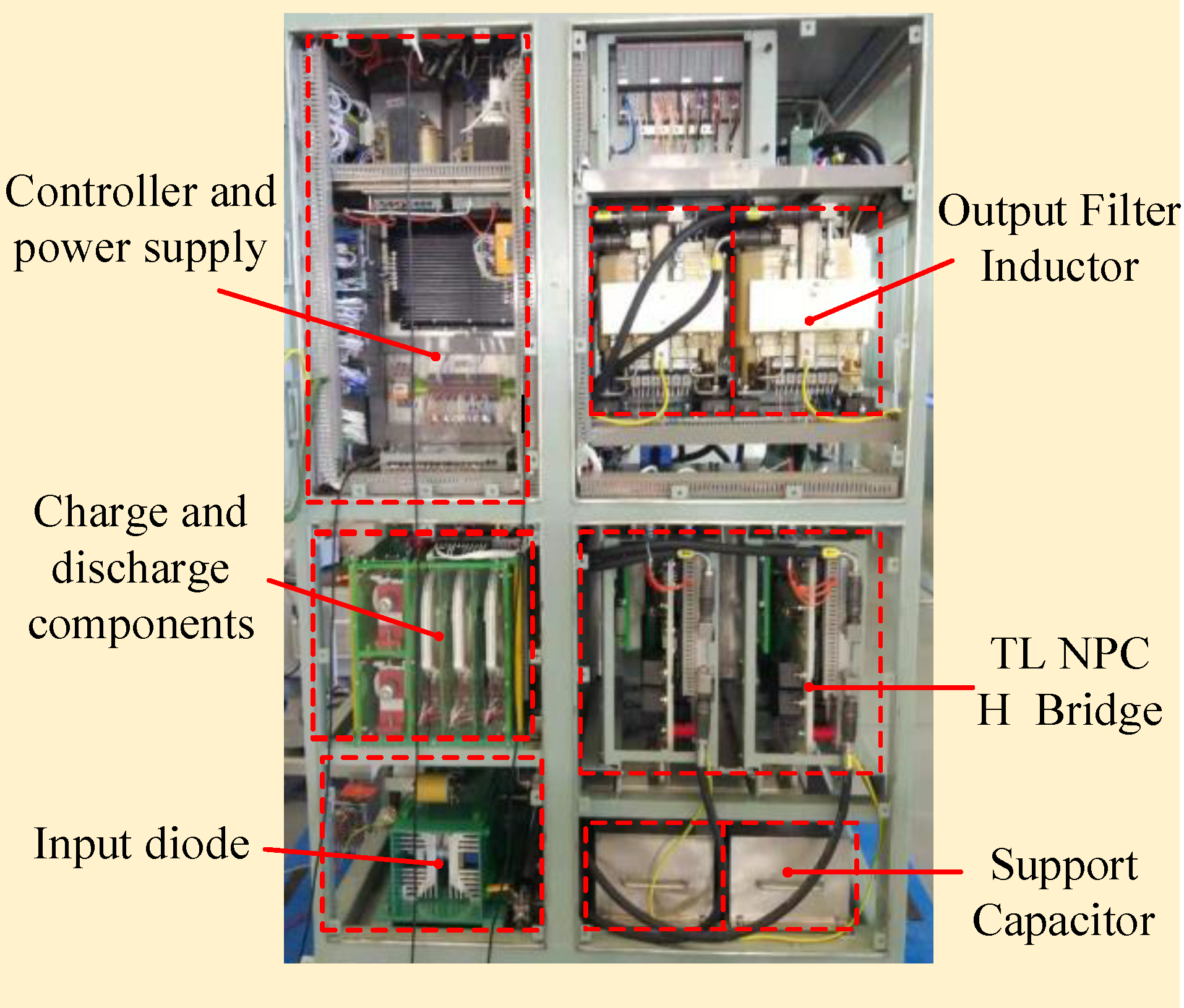
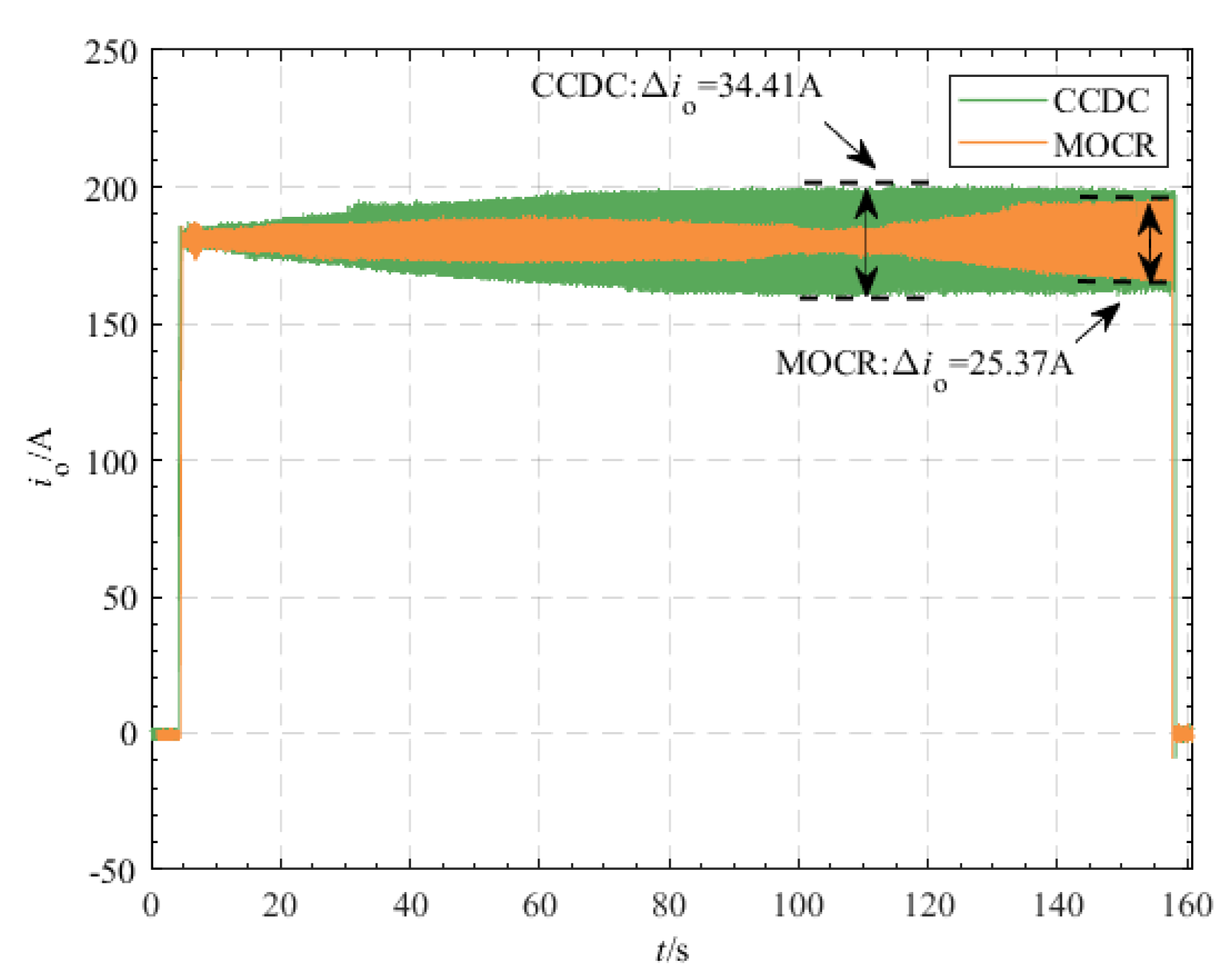
5. Experimental Verification

In this paper, a 1:1 test prototype is designed as shown in Figure 15, and the parameters of the main circuit are shown in Table 2. The output current ripple index is designed to be less than 20% Io. The prototype experiment uses the ultracapacitor as the load and adopts the constant current charging mode.
Figure 16 shows the experimental waveform of the output current of the ultracapacitor charged from 0 V to the rated voltage at the constant current 180 A. The maximum current ripple is 34.41 A with the CCDC strategy and 25.37 A with the MOCR strategy, which is 26.27% less. The output current ripple in the whole charging process is smaller than that of the CCDC strategy, and the trend of ripple current during charging is consistent with the theoretical analysis shown in Figure 11, which verifies the correctness of the above theoretical analysis.
In the initial stage, the converter prototype is designed according to the theoretical analysis results of the CCDC strategy. In order to meet the output current ripple index, the output filter inductor is taken to be larger, and its weight and size are also larger. The physical picture is shown in Figure 17a, with a weight of 142 kg and a three-dimensional size of 211 mm (height) × 329 mm (width) × 298 mm (depth).
According to the theoretical analysis results and experimental results of the MOCR strategy studied in this paper, the output filter inductance value of the prototype can be reduced to 6 mH; the three-dimensional figure is shown in Figure 17b. The weight is 120 kg, and the three-dimensional size is 203 mm (height) × 309 mm (width) × 277 mm (depth). Compared with the filter inductor before optimization, weight, volume and loss are respectively reduced by 13.98%, 14.94%, and 11.54%.

6. Conclusions

For the TL-PSFB converter operating in a current-fed mode in DC microgrid, this paper analyzes and points out the problems such as poor current ripple performance and non-compliance with the static operating point design principle of the traditional CCDC strategy. A MOCR strategy is proposed and the performance of the two strategies is quantitatively compared in four aspects. Both experimental and theoretical analyses prove that the proposed MOCR strategy has better performance than the traditional CCDC strategy. In fact, the MOCR strategy adds a degree of control freedom to the CCDC strategy. Adopting the idea of software-based hardware functions avoids the use of high-order filters when a small current ripple index is required. To a certain extent, the power density and efficiency of the converter are improved and the engineering cost is reduced.

Author Contributions

Conceptualization, H.W., G.Y. and X.F.; methodology, H.W., G.Y., X.Z. and F.X.; software, H.W. and G.Y.; validation, H.W., G.Y., F.X. and X.F.; writing—original draft preparation, H.W., G.Y. and W.K. All authors have read and agreed to the published version of the manuscript.

Funding

This research was funded by the National Natural Science Foundation of China, grant number 51907199.

Institutional Review Board Statement

Not applicable.

Informed Consent Statement

Not applicable.

Conflicts of Interest

The authors declare no conflict of interest. The funders had no role in the design of the study; in the collection, analyses, or interpretation of data; in the writing of the manuscript, or in the decision to publish the results.

References

  1. Wen, S.; Zhao, T.; Tang, Y.; Xu, Y.; Zhu, M.; Huang, Y. A Joint Photovoltaic-Dependent Navigation Routing and Energy Storage System Sizing Scheme for More Efficient All-Electric Ships. IEEE Trans. Transp. Electrif. 2020, 6, 1279–1289. [Google Scholar] [CrossRef]
  2. Sadiq, M.; Ali, S.W.; Terriche, Y.; Mutarraf, M.U.; Hassan, M.A.; Hamid, K.; Ali, Z.; Sze, J.Y.; Su, C.-L.; Guerrero, J.M. Future Greener Seaports: A Review of New Infrastructure, Challenges, and Energy Efficiency Measures. IEEE Access 2021, 9, 75568–75587. [Google Scholar] [CrossRef]
  3. Pinheiro, J.R.; Barbi, I. The Three-Level ZVS-PWM DC-to-DC Converter. IEEE Trans. Power Electron. 1993, 8, 7. [Google Scholar] [CrossRef]
  4. Ruan, X.; Li, B.; Chen, Q.; Tan, S.-C.; Tse, C.K. Fundamental Considerations of Three-Level DC–DC Converters: Topologies, Analyses, and Control. IEEE Trans. Circuits Syst. Regul. Pap. 2008, 55, 3733–3743. [Google Scholar] [CrossRef]
  5. Yang, G.; Xiao, F.; Fan, X.; Wang, R.; Liu, J. Three-Phase Three-Level Phase-Shifted PWM DC–DC Converter for Electric Ship MVDC Application. IEEE J. Emerg. Sel. Top. Power Electron. 2017, 5, 162–170. [Google Scholar] [CrossRef]
  6. Liu, J.; Xiao, F.; Ma, W.; Fan, X.; Chen, W. PWM-Based Sliding Mode Controller for Three-Level Full-Bridge DC-DC Converter That Eliminates Static Output Voltage Error. J. Power Electron. 2015, 15, 378–388. [Google Scholar] [CrossRef]
  7. Liu, F.; Chen, Y.; Hu, G.; Ruan, X. Modified Three-Phase Three-Level DC/DC Converter with Zero-Voltage-Switching Characteristic-Adopting Asymmetrical Duty Cycle Control. IEEE Trans. Power Electron. 2014, 29, 6307–6318. [Google Scholar] [CrossRef]
  8. Zhang, Z.; Ruan, X. A Novel Double Phase-Shift Control Scheme for Full-Bridge Three-Level Converter. In Proceedings of the Twentieth Annual IEEE Applied Power Electronics Conference and Exposition, 2005, APEC 2005, Austin, TX, USA, 6–10 March 2005; Volume 2, pp. 1240–1245. [Google Scholar]
  9. Liu, D.; Wang, Y.; Deng, F.; Chen, Z. Triple-Phase-Shift Modulation Strategy for Diode-Clamped Full-Bridge Three-Level Isolated DC/DC Converter. IEEE Access 2020, 8, 2750–2759. [Google Scholar] [CrossRef]
  10. Guo, Y.; Yang, Z.; Yin, Y.; Cao, H. Digital Control of Hybrid Full Bridge Three-Level LLC Resonant Converter Based on SiC MOSFET. In Proceedings of the 2018 IEEE International Power Electronics and Application Conference and Exposition (PEAC), Shenzhen, China, 4–7 November 2018; pp. 1–6. [Google Scholar]
  11. Haga, H.; Kurokawa, F. Modulation Method of a Full-Bridge Three-Level LLC Resonant Converter for Battery Charger of Electrical Vehicles. IEEE Trans. Power Electron. 2017, 32, 2498–2507. [Google Scholar] [CrossRef]
  12. Deng, F.; Chen, Z. Control of Improved Full-Bridge Three-Level DC/DC Converter for Wind Turbines in a DC Grid. IEEE Trans. Power Electron. 2013, 28, 314–324. [Google Scholar] [CrossRef]
  13. Shi, Y.; Yang, X. Zero-Voltage Switching PWM Three-Level Full-Bridge DC–DC Converter with Wide ZVS Load Range. IEEE Trans. Power Electron. 2013, 28, 4511–4524. [Google Scholar] [CrossRef]
  14. Liu, F.; Yan, J.; Ruan, X. Zero-Voltage and Zero-Current-Switching PWM Combined Three-Level DC/DC Converter. IEEE Trans. Ind. Electron. 2010, 57, 1644–1654. [Google Scholar] [CrossRef]
  15. Ruan, X.; Li, B. Zero-Voltage and Zero-Current-Switching PWM Hybrid Full-Bridge Three-Level Converter. IEEE Trans. Ind. Electron. 2005, 52, 213–220. [Google Scholar] [CrossRef]
  16. Lin, B.-R. Hybrid DC/DC Converter Based on Dual Three-Level Circuit and Half-Bridge Circuit. IET Power Electron. 2016, 9, 817–824. [Google Scholar] [CrossRef]
  17. Lin, B.-R.; Hou, B.-R. Analysis and Implementation of a Zero-Voltage Switching Pulse-Width Modulation Resonant Converter. IET Power Electron. 2014, 7, 148–156. [Google Scholar] [CrossRef]
  18. Lin, B.-R.; Chen, C.-C. Zero Voltage Switching DC Converter for High-Input Voltage and High-Load Current Applications. IET Power Electron. 2014, 7, 124–131. [Google Scholar] [CrossRef]
  19. Shi, Y.; Xi, J.; Wang, X.; Gui, X.; Yang, X. Large-Power ZVZCS Full-Bridge Three-Level DC–DC Converter with Wide Operation Range and Its Application in Sapphire Crystal Furnace Power Supply. IEEE J. Emerg. Sel. Top. Power Electron. 2020, 8, 4191–4208. [Google Scholar] [CrossRef]
  20. Liu, P.; Duan, S. Analysis of the Neutral-Point Voltage Self-Balance Mechanism in the Three-Level Full-Bridge DC−DC Converter by Introduction of Flying Capacitors. IEEE Trans. Power Electron. 2019, 34, 11736–11747. [Google Scholar] [CrossRef]
  21. Guo, Z.; Sun, K.; Sha, D. Improved ZVS Three-Level DC–DC Converter with Reduced Circulating Loss. IEEE Trans. Power Electron. 2016, 31, 6394–6404. [Google Scholar] [CrossRef]
  22. Canales, F.; Barbosa, P.; Lee, F.C. A Zero-Voltage and Zero-Current Switching Three-Level DC/DC Converter. IEEE Trans. Power Electron. 2002, 17, 898–904. [Google Scholar] [CrossRef]
  23. Li, Y.; Li, F.; Zhao, F.-W.; You, X.-J.; Zhang, K.; Liang, M. Hybrid Three-Level Full-Bridge Isolated Buck–Boost Converter with Clamped Inductor for Wider Voltage Range Application. IEEE Trans. Power Electron. 2019, 34, 2923–2937. [Google Scholar] [CrossRef]
  24. Guo, Z.; Sha, D.; Liao, X. Hybrid Three-Level and Half-Bridge DC–DC Converter with Reduced Circulating Loss and Output Filter Inductance. IEEE Trans. Power Electron. 2015, 30, 6628–6638. [Google Scholar] [CrossRef]
  25. Liu, D.; Wang, Y.; Zhang, Q.; Chen, Z. ZVZCS Full-Bridge Three-Level DC/DC Converter with Reduced Device Count. IEEE Trans. Power Electron. 2020, 35, 9965–9970. [Google Scholar] [CrossRef]
  26. Wu, H.; Lu, Y.; Sun, K.; Xing, Y. Phase-Shift-Controlled Isolated Buck-Boost Converter with Active-Clamped Three-Level Rectifier (AC-TLR) Featuring Soft-Switching Within Wide Operation Range. IEEE Trans. Power Electron. 2016, 31, 2372–2386. [Google Scholar] [CrossRef]
  27. Liu, D.; Wang, Y.; Deng, F.; Chen, Z. Balanced Power Device Currents Based Modulation Strategy for Full-Bridge Three-Level DC/DC Converter. IEEE Trans. Power Electron. 2020, 35, 2008–2022. [Google Scholar] [CrossRef]
  28. Liu, D.; Deng, F.; Zhang, Q.; Chen, Z. Zero-Voltage Switching PWM Strategy Based Capacitor Current-Balancing Control for Half-Bridge Three-Level DC/DC Converter. IEEE Trans. Power Electron. 2018, 33, 357–369. [Google Scholar] [CrossRef]
  29. Tian, K.; Li, T.; Yuen, K.F. A Common-Mode Voltage Reduction Modulation for a Phase-Shift DC-DC Converter. In Proceedings of the 2018 IEEE International Power Electronics and Application Conference and Exposition (PEAC), Shenzhen, China, 4–7 November 2018; pp. 1–5. [Google Scholar]
  30. Chen, W.; Ruan, X.; Chen, Q.; Ge, J. Zero-Voltage-Switching PWM Full-Bridge Converter Employing Auxiliary Transformer to Reset the Clamping Diode Current. IEEE Trans. Power Electron. 2010, 25, 1149–1162. [Google Scholar] [CrossRef]
  31. Chen, W.; Ruan, X. Zero-Voltage-Switching PWM Hybrid Full-Bridge Three-Level Converter with Secondary-Voltage Clamping Scheme. IEEE Trans. Ind. Electron. 2008, 55, 644–654. [Google Scholar] [CrossRef]
  32. Zhang, X.; Wang, R.; Xiao, F.; Fan, X.; Yang, G.; Yang, B. Design of Highly Compact Short-Time Duty Power Inductors for Supercapacitor Charging Applications. IET Power Electron. 2020, 13, 4377–4385. [Google Scholar] [CrossRef]
  33. Dowell, P.L. Effects of Eddy Currents in Transformer Windings. Proc. Inst. Electr. Eng. 1966, 113, 1387–1394. [Google Scholar] [CrossRef]
Figure 1. Topology of MVDC renewable energy microgrid.
Energies 15 06444 g001
Figure 2. Topology of dual-output TL-PSFB converter.
Energies 15 06444 g002
Figure 3. Principle of PS-PWM.
Energies 15 06444 g003
Figure 4. Output voltage waveform of uab. (a) 0 < dα < dγ, (b) dγ < dα < dθ, (c) dθ < dα < 1/2.
Energies 15 06444 g004
Figure 5. Relationship between dα, dθ and the THD of primary voltage.
Energies 15 06444 g005
Figure 6. The output harmonic equivalent circuit of the rectifier bridge.
Energies 15 06444 g006
Figure 7. Comparison of current ripple calculation and simulation of filter inductor under different dθ and dα. (a) dα = 1/12, dθ = 1/3 (0 < dα < dγ). (b) dα = ¼, dθ = 3/8 (dγ < dα < dθ). (c) dα = 2/5, dθ = 3/10 (dθ < dα < 1/2).
Energies 15 06444 g007
Figure 8. Output current ripple corresponding to different dθ and dα.
Energies 15 06444 g008
Figure 9. Output current ripple corresponding to different dθ and dα (top view).
Energies 15 06444 g009
Figure 10. Diagram of constant current control with the MOCR strategy.
Energies 15 06444 g010
Figure 11. Comparison of current ripple analytical calculations between CCDC and MOCR.
Energies 15 06444 g011
Figure 12. Comparison of volume and weight of output filter inductors for different parameters in Table 1.
Energies 15 06444 g012
Figure 13. Comparison of losses of output filter inductors for different parameters in Table 1.
Energies 15 06444 g013
Figure 14. Comparison of the THD of uab using MOCR and CCDC.
Energies 15 06444 g014
Figure 15. The physical picture of the dual-output TL-PSFB converter test prototype.
Energies 15 06444 g015
Figure 16. The experimental waveform of the output current of the two strategies.
Energies 15 06444 g016
Figure 17. Three-dimensional comparison of the filter inductor before and after optimization. (a) Physical picture of the filter inductor before optimization, (b) 3D picture of the filter inductor after optimization.
Energies 15 06444 g017
Table 1. Different output current ripple indexes requiring the value of minimum filter inductance corresponding to two strategies.
ioCCDC: Lf/mHMOCR: Lf/mH
5% Io29.3922.52
10% Io14.7011.26
15% Io9.807.51
20% Io7.355.63
25% Io5.884.50
Table 2. The parameters of the main circuit of the test prototype.
ParametersValueParametersValue
Ud/kV4NT4:3:3
Uo/kV0–2Lr/μH40
Io/A180Lf/mH8
f/kHz1C1, C2/mF4
Publisher’s Note: MDPI stays neutral with regard to jurisdictional claims in published maps and institutional affiliations.

