Article

New Class of Power Converter for Performing the Multiple Operations in a Single Converter: Universal Power Converter

1
Department of Electrical & Electronics Engineering, Anil Neerukonda Institute of Technology and Science (A), Visakhapatnam 531162, India
2
Department of Electrical & Electronics Engineering, GVP College of Engineering for Women, Visakhapatnam 531162, India
3
Faculty of Engineering and Technology, Future University in Egypt, Cairo 11835, Egypt
4
Energy Technology Program, School of Engineering Technology, Purdue University, West Lafayette, IN 47907, USA
*
Author to whom correspondence should be addressed.
Energies 2022, 15(17), 6293; https://doi.org/10.3390/en15176293
Submission received: 25 June 2022 / Revised: 18 August 2022 / Accepted: 22 August 2022 / Published: 29 August 2022

Abstract

:
Universal power converters (UPCs) have aroused significant attention in performing multiple operations in a single power converter. Furthermore, they contribute to economic operation and improved system performance. In this work, a new configuration of the universal power converter (UPC) was proposed by using a simple switching arrangement. It can perform different modes of operations, such as AC–DC, DC–DC, DC–AC, AC–AC, and cyclo-converter operations. In DC–DC conversion, the proposed configuration can perform buck mode, boost mode, and buck–boost mode of operations. Moreover, in DC–AC conversion, it gives better total harmonic distortion (THD). The effectiveness of the proposed configuration was verified by an extensive simulation, using MATLAB/Simulink environment. A low-power prototype circuit was designed to test the viability of the proposed circuit configuration and validated with simulation results.

1. Introduction

Universal power converters (UPCs) have many advantages over conventional solutions [1,2,3,4] employing multiple single converters; the advantages include lower-cost characteristics, compact size, high power density, etc. This class of power converters is called “universal” because the inputs and outputs of the converters can be DC or AC. Therefore, they can be employed in various applications, including, but not limited to, photovoltaic (PV) power generation, battery–utility interfaces, and nanogrids. Therefore, UPCs are a suitable fit for nanogrids, electric vehicles (EVs), and photovoltaic (PV) applications [5,6,7].
Power electronic converters are classified into two types: non-isolated and isolated. In an isolated converter, the multi-winding transformer obtains high voltage gain and isolation between output and input ports. However, it has some drawbacks: more voltage stress, losses in the converter, converter size, and less converter efficiency [8,9,10]. Therefore, non-isolated converters have emerged in this field. There are several converter configurations in the category of non-isolated converters. Boost capacitor and passive clamp circuit-based DC–DC converters are suggested in Reference [11]. They improve the voltage gain and reduce voltage-stress spikes. However, they have a higher part count compared to the high-gain voltage converters, and where the coupled inductor size is larger than it is in the ordinary inductor. Similarly, a coupled-inductor and voltage-multiplier cell-based boost hybrid converter is proposed for high-gain applications [12]. A converter based on a switched inductor and capacitor hybrid is suggested in Reference [13] for improving converter performance. This converter operation is based on energizing the inductors in series and discharging capacitors in parallel or vice versa. Nevertheless, this converter has more device count, leading to an increased converter cost and size. Furthermore, a new converter topology is presented for nanogrid application in Reference [14] and fuel application in Reference [15].
The combinations of two or more conventional converter features are used to derive a kind of a new DC–DC converter topology, and they are introduced as hybrid converters in References [16,17,18,19,20] for hybrid (DC–AC and DC–DC) power-conversion applications. A hybrid converter is suggested in Reference [21], using a phase-shifted full-bridge for electric vehicle charger applications. In this configuration, the limitations of the conventional PSFB converter are overcome. A hybrid full-bridge DC-to-DC converter is introduced for radiofrequency applications in Reference [7] to overcome the drawbacks of the filter size across the load and circulating currents of a conventional full-bridge converter. A hybrid step-down power factor correction (PFC) converter is presented in Reference [22]. It has combined features of boost PFC and buck PFC converter to improve the power factor. A switched-capacitor-based hybrid high-gain DC–DC converter is proposed in Reference [23]. It is derived from buck, boost, and buck–boost topologies. However, the number of capacitors causes extra cost and enhanced size.
A new topology of the universal power converter is proposed in Reference [24] to obtain all possible power conversions in a single stage, viz AC–AC and DC–AC. However, this converter has a complex structure with many switching devices. Along similar lines, another universal converter for battery-charging applications is suggested in Reference [25] and is suitable only for AC–DC and DC–DC with the buck–boost mode of operation. However, it is not ideal for DC–AC, and AC–AC power-conversion applications. A fully modular configuration is developed in References [21,26] for universal (AC–DC, DC–AC, and DC–DC) power-conversion applications. Moreover, a novel solar converter for applicability in DC and AC microgrid is proposed in Reference [27] and a universal power converter using buck–boost converter and full bridge circuit is proposed in Reference [28]. However, these converters are not fully universal in view of different types of sources and loads.
In this paper, a novel universal power converter that is first of its kind is introduced; the network topology looks like a front-end semiconductor switch connected to an H-bridge network. The application field of the proposed configuration can be used to perform multiple operations in a single converter, such as DC–DC, AC–DC, AC–AC, DC–AC, and cyclo-converter operations. Therefore, it is suitable for (i) renewable-energy integration with solar PV roof-top application, (ii) remote village DC microgrid application, (iii) flexibly connecting to AC or DC loads in a small commercial area application, etc.
The paper is arranged as follows: Section 2 describes the suggested topology and various operation modes. The parameter design and power analysis and comparative analysis are presented in Section 3. The simulation and experimental results in various configurations are discussed in Section 4. The proposed work is concluded in Section 5.

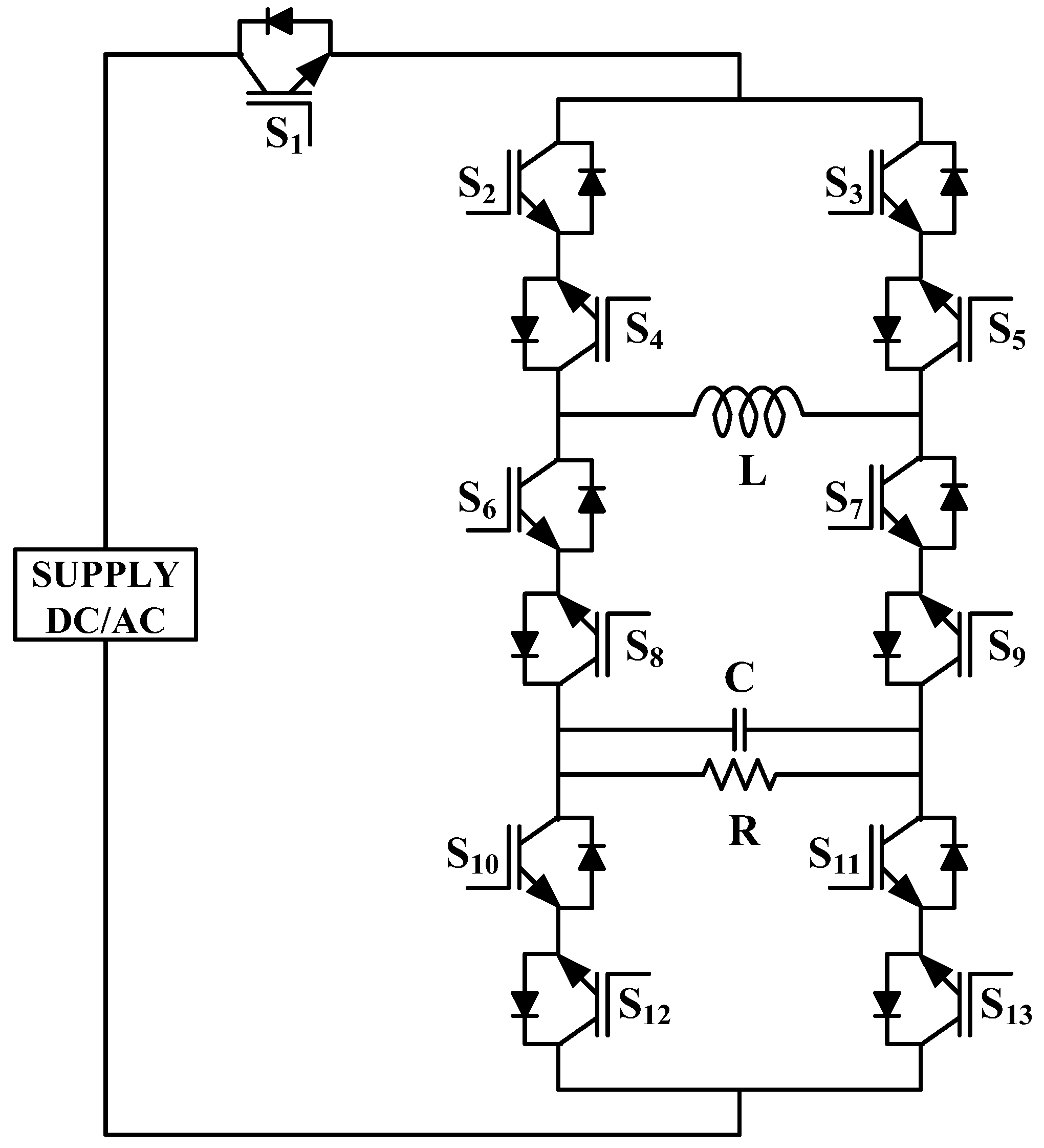
2. Proposed Universal-Power-Converter Configuration and Modes of Operation

The UPC is a relatively new class of power converter. The schematic circuit diagram of the proposed UPC is shown in Figure 1. Figure 2, Figure 3, Figure 4, Figure 5, Figure 6, Figure 7 and Figure 8 show different circuit configurations of the developed converter, along with their equivalent circuits. The current through the inductor (iL) and the voltage across the capacitor (vC) are also presented in each mode of operation.
The proposed converter has the following features:
(1)
The proposed configuration has a reduced number of components compared with the individual conventional converters combined to obtain different modes of voltage conversion.
(2)
It can perform the AC–DC, DC–DC, DC–AC, and AC–AC (cyclo-converter and ac voltage converter) operations with the single converter.

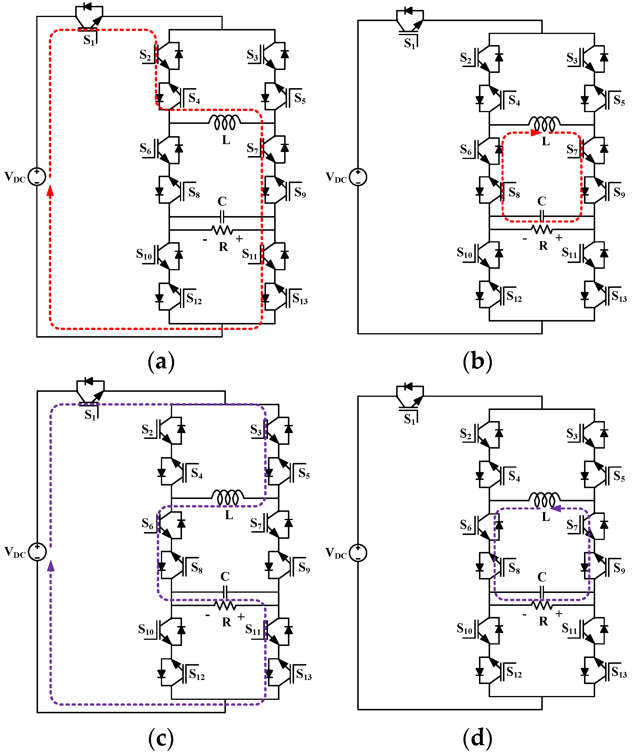
2.1. Various Circuit Configurations: DC–DC Converter Operation

2.1.1. DC–DC Converter (Buck Mode)

Switching State 1

In this operating mode, the switching action happens between the switches S1, S2, S7, and S10; the remaining power semiconductor switches are kept off. Now, the input DC source (VDC) supplies energy to the load, and the inductor is energized accordingly. The corresponding circuit in this Switching State-1 is shown in Figure 2a.

Switching State 2

During this switching mode, the supply input is switched off, and the inductor (L) delivers its stored energy to the load (R) through the active switches S7 and S8. The circuit in this mode of operation is represented in Figure 2b.
The output voltage (V0) expression in buck operation can be expressed as follows:
V 0 = V D C d
where d is the duty ratio.

2.1.2. DC–DC Converter (Boost Mode)

Switching Mode 1

In this operating mode, active switches S1, S2, S7, and S11 are turned on; the corresponding current flow direction is illustrated in Figure 2c. In this switching state, the voltage source charges the inductor, and the capacitor delivers the stored energy to the load R.

Switching Mode 2

Figure 2d shows the equivalent circuit in this mode of operation. During this mode, stored energy in the inductor is discharged and delivered to the capacitor and load (R) through the switches S1, S2, S7, and S10.
The output voltage (V0) expression in boost operation can be expressed as follows:
V 0 = V D C ( 1 - d )
where d is the duty ratio.

2.1.3. DC–DC Converter (Buck–Boost Mode)

Switching Mode 1

In this mode of operation, controlled devices S1, S2, S7, and S11 are switched on, and the inductor (L) is energized by the input supply (VDC). Similarly, the capacitor releases its stored energy to the load (R). The direction of current flow in this mode of operation is illustrated in Figure 2e.

Switching Mode 2

In this switching operation, the energy stored in the inductor is released to the load (R) through the switches S7 and S8; Figure 2f shows the equivalent circuit.
The output voltage expression in the buck–boost mode can be expressed as follows:
V 0 = V D C d ( 1 - d )
where d is the duty ratio.

2.2. Various Circuit Configurations: DC–AC Conversion (Inverter Operation)

The proposed topology is operated in the inverter configuration, and the corresponding modes of operation, along with their equivalent circuits, are illustrated in Figure 3a–d.
Mode 1:
The switches S1, S2, S7, and S10 are switched on in this mode, and the source port energizes the inductor; the resulting equivalent circuit is depicted in Figure 3a.
Mode 2:
The supply voltage remains off in this mode, and the energy stored in the inductor is de-energized by the devices S7 and S8; the resulting equivalent circuit is depicted in Figure 3b, wherein Modes 1 and 2 provide a positive output voltage level.
Mode 3:
The switches S1, S3, S6, and S11 are turned on, and the inductor is energized by the input voltage; the resultant equivalent circuit is shown in Figure 3c.
Mode 4:
The energy stored in the inductor is de-energized through the switches S6 and S9 in this mode, and the resultant circuit is shown in Figure 3d. Modes 3 and 4 generate the negative level of output voltage.
The expression of the rms value for fundamental component of the output voltage is as follows:
V r m s = [ 1 π 0 π V D C 2 ( t ) d t ]
where VDC is the input voltage.

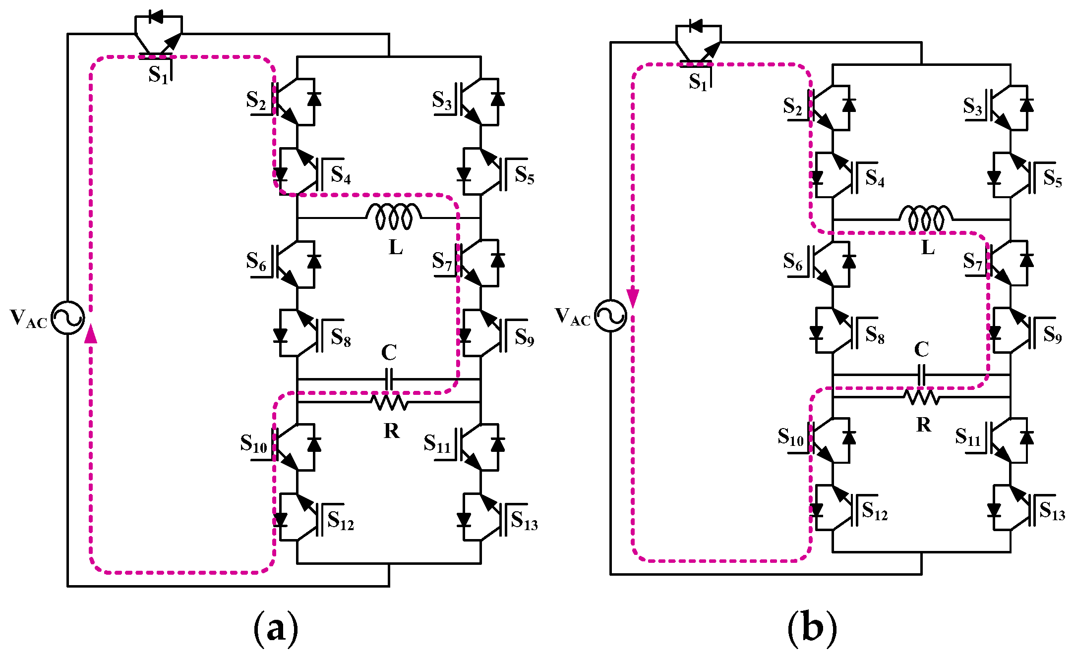
2.3. Various Circuit Configurations: AC–DC Conversion (Rectifier Operation)

The designed UPC can also be operated as a rectifier, as shown in Figure 4a,b. This configuration has two modes of operation with respect to the resistive load.
Mode 1:
The switches S1, S2, S7, and S10 are fired in the positive half cycle at an angle, α. From ωt = α to π, the switches conduct, and the load voltage varies from 0 to Vm sinωt. The current takes the path VAcph-S1-S2-L-S7-LOAD-S10-VACN, and the load voltage is in phase with the load current in Figure 4a.
Mode 2:
In the negative half cycle, the switches S13, S8, and S5 are made to conduct from ωt = π to 2π. In Figure 4b, it can be seen that the current flows through the path VAcph-S13-S8-LOAD-L-S5-VACN. The output voltage can be determined by using the following equation:
V 0 = 1 π α π V m s i n ω t d ( ω t )

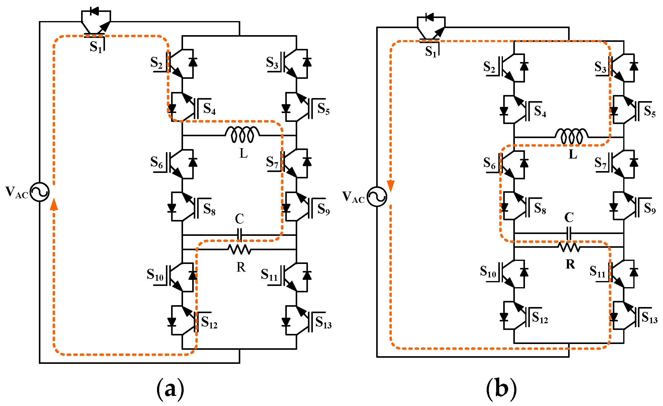
2.4. Various Circuit Configurations: AC–AC Conversion (AC Voltage Controller Operation)

Mode 1:
During the positive half cycle, switches S1, S4 and S7 are fired at a delay angle, α, and it conducts from ωt = α to π for resistive load. The path for the flow of the current, as shown in Figure 5a, is given by VAcph-S1-S2-L-S4- S7-LOAD-S10-VACN for resistive load.
Mode 2:
In the negative half cycle, the switches S6 and S5 are conducted from ωt = π + α to 2π, and the current flows through the path VAcph-S12-S9-LOAD-S4-L-VACN, as shown in Figure 5b. The RMS value of output voltage can be determined by using the following equation:
V O r = [ 1 π α π V m 2 s i n 2 ω t d ( ω t ) ] 1 2
where α is the delay angle.

2.5. Various Circuit Configurations: AC–AC Conversion (Cyclo-Converter Operation)

The operation of the cyclo-converter is described here for step-down frequency (i.e., output frequency = supply frequency/2). The switching combination in step-down frequency is shown in Table 1. Similarly, it can be extended to the step-up frequency operation of the cyclo-converter. The corresponding switching combination at different output frequencies is show in Table 2. The theoretical waveforms of the proposed converter in step-down and step-up frequency modes of operation are illustrated in Figure 6a,b respectively.
Mode 1:
The switches S1, S2, S7, and S10 are forward biased in the positive half cycle of input voltage, as shown in Figure 7a. These are triggered at α = 0 and conduct from ωt = α to π for a resistive load (R). The path for the flow of current in the circuit is given by VAcph-S1-S2-L-S7-LOAD-S10-VACN.
Mode 2:
In the negative half cycle, the switches S13, S8, and S5 are switched on, as given in Figure 7b. These are conducted from ωt = π to 2π for resistive load. The path for the flow of current in the circuit is given by VAcph-S13-LOAD-S8-L-S5-VACN.
Mode3:
In the positive half cycle, switches S1, S3, S6, and S11 are forward biased, as shown in Figure 7c. These are conducted from ωt = 2 π to 3π for resistive load. The path for the flow of current in the circuit is given by VAcph-S3-L-S6-LOAD-S11-VACN.
Mode4:
In the negative half cycle, the switches S12, S9, and S4 are turned on, as shown in Figure 7d. It is conducted from ωt = 3π to 4π for resistive load. The path for the flow of the current in the circuit is given by VAcph-S12-LOAD-S9-L-S4-VACN.

3. Parameter Design and Power Loss Analysis

3.1. Parameter Design Procedure

The parameter design of circuit components depends mainly on the type of capacitor, inductor, switching frequency, and duty ratio, as detailed in Reference [29], and as given in Equations (7)–(13).
Step 1: The maximum and minimum power are given by the following:
P 0 m a x = V 0 I 0 m a x P 0 m i n = V 0 I 0 m i n
Step 2: The load-resistance maximum and minimum values are calculated as follows:
R L m i n = V 0 I 0 m a x R L m a x = V 0 I 0 m i n
Step 3: The output voltage conversion gain of the converter is as follows:
M V D C m i n = V 0 V D C m a x M V D C n o m = V 0 V D C M V D C m a x = V 0 V D C m i n
Step 4: The duty ratio range is determined by the following equations:
d m i n = M V D C m i n η d n o m = M V D C n o m η d m a x = M V D C m a x η
where η is the converter efficiency.
Equations (9)–(11) give the proper selection of the duty ratio, which is related to voltage conversion and efficiency.
Step 5: The minimum values of inductance are determined as follows:
L m i n = R L m a x ( 1 d m i n ) 2 f s
Capacitance value can be obtained as follows:
C m i n = D m a x V 0 V c p p R L m a x f s
where, V0 is the output voltage, Dmax is the maximum duty ratio, fs is the switching frequency, RLmax is the maximum load resistance, and Vcpp is the peak-to-peak value of the capacitor.
V c p p = V r 2
The ripple voltage (Vr) is 1% V0.
The above expression shows the relation between the duty ratio, load, and inductance parameters. The calculated parameter values are listed in Table 3.

3.2. Power-Loss Analysis

The conduction and switching losses constitute the losses in the converters [30] and are given by Equations (14)–(17):
P l o s s = P c o n + P s w
The conduction losses are determined as shown below:
P c o n = 1 T 0 T ( R o n i F + V F o ) i F d t
where iF, VFo, Ron, and T are the current in the forward direction, forward voltage, on-state device resistance, and switching period, respectively.
The total switching losses are determined as follows:
P s w = 1 n j = 1 n [ E O F F j ( i F , V O F F ) + E O N j ( i F , V O F F ) ]
where EOFF and EON are the energy dissipation during switching.
Therefore, efficiency can be determined as follows:
η = P o u t P o u t + P s w + P c o n

3.3. Comparative Analysis

It is always better to perform a comparative analysis with the other counter parts to gain insight into and determine the superiority of the proposed converter topology. The comparison of the proposed UPC with the other recently proposed hybrid converters in terms of number of power semiconductor switches, reactive elements, and modes of operation is shown in Table 4. It is observed that the proposed UPC offers a greater number of operating modes in one converter, with nearly the same total-number-of-parts count. However, every converter has its own merits and demerits.

4. Results and Discussions

4.1. Simulation Results

Using the MATLAB/Simulink environment, simulations were run to analyze the performance of the proposed converter. The test was conducted in different modes of operation, such as DC–DC, DC–AC, AC–DC, AC–AC, and cyclo-converter configurations. The input voltage, duty cycle, and switching frequency were 50 V, 60%, and 10 kHz, respectively. The proposed UPC was tested in the DC–DC conversion with the buck mode of operation. The output voltage and current flow through the inductor are shown in Figure 8a,b. The proposed configuration is operated in boost and buck–boost modes. The corresponding output voltage and inductor current are depicted in Figure 8c–f, respectively. From Figure 8a,c,e, it is clear that the results are close to the theoretical values and verified with output voltage expressions given by Equations (1)–(3). In the inverter configuration, the input voltage is taken as 50 V, and the corresponding load voltage and FFT analysis are illustrated in Figure 9a,b. It is observed that the proposed configuration has 8.56%THD in inverter operation. The performance of the proposed configuration under different modes of operation, such as rectifier (AC–DC), AC voltage controller (AC–AC), and cyclo-converter operations, was tested; the input voltage of 48 Vmax was fed to the converter, as shown in Figure 10a. Figure 10b depicts load voltage in rectifier mode at a firing angle of 30°. For the AC voltage controller operation, the controlled output voltage with a firing angle of 90° is shown in Figure 10c. The performance of the proposed configuration in the cyclo-converter operation was verified at a firing angle of 0°, and the corresponding output voltage is illustrated in Figure 10d. These results confirmed that the proposed UPC could perform multiple operations in a single converter.
Figure 8. Simulation results of proposed UPC in DC–DC operation: (a) buck output voltage, (b) inductor current during buck operation, (c) boost output voltage, (d) inductor current during boost operation, (e) buck–boost output voltage, and (f) inductor current during buck–boost mode.
Energies 15 06293 g008aEnergies 15 06293 g008b

4.2. Experimental Verification

A 100 W laboratory prototype was developed; to validate the low-power prototype, a circuit was developed in the laboratory to demonstrate the feasibility and benefits of the proposed UPC. It was tested under buck, boost, buck–boost, and inverter operations. In DC–DC conversion, the test was performed with the input voltage of 50 V, duty cycle of D = 60%, inductor value of 3 mH, a capacitor value of 600 µF, and switching frequency of 10 kHz. The control module dSPACE1104 was used as a core controller for generating a controlling signal for active switches IGBTs (STGW30NC120HD). For the buck mode of operation, the experimental output voltage and current flow in the inductor are shown in Figure 11a,b respectively. Similarly, output voltage and inductor current in boost and buck–boost mode of operations are illustrated in Figure 11c–f, respectively. It can be observed that Figure 11a,c,e are close to both the theoretical and simulation results. Afterward, the proposed UPC was tested in an inverter configuration with an input voltage of 50 V. The corresponding output voltage and FFT analysis are depicted in Figure 12a,b, respectively. The proposed converter was also tested in rectifier, AC voltage controller, and cyclo-converter operations at the input voltage of 48 V. The corresponding input and output voltages are depicted in Figure 13a–d, respectively. The efficiency of the converter in the different modes of operation is shown in Figure 14a, and a power-loss analysis of the proposed converter in various operations is depicted in Figure 14b. Snapshots of the hardware experimentation on the UPC prototype circuit in the laboratory are illustrated in Figure 15.

5. Conclusions

In this paper, a new class of power converter called UPC is proposed for performing multiple operations in a single converter, such as DC–DC, DC–AC, AC–DC, and AC–AC (cyclo-converter and AC voltage converter) operations. The operating principle and different modes of operations were explained in detail. In DC–DC conversion, it can be performed as buck, boost, and buck–boost operations. Similarly, in DC–AC conversion, the proposed UPC gives a better %THD. Finally, the proposed converter operation and performance were validated with both simulation and experimental results.

Author Contributions

D.M., D.P. and R.S. designed the problem under study and performed the simulations and obtained the results; D.M., D.P. and R.S. wrote the paper, which was further reviewed by A.Y.A. and A.E.-S. All authors have read and agreed to the published version of the manuscript.

Funding

This research received no external funding.

Institutional Review Board Statement

Not applicable.

Informed Consent Statement

Not applicable.

Data Availability Statement

Not applicable.

Conflicts of Interest

The authors declare no conflict of interest.

References

  1. Zhang, H.; Dong, D.; Jing, M.; Liu, W.; Zheng, F.; Samiullah, M.D.; Atif, I.; Imtiaz, A.; Pandav Kira, M. Voltage Lift Switched Inductor Double Leg Converter with Extended Duty Ratio for DC Microgrid Application. IEEE Access 2021, 9, 85310–85325. [Google Scholar]
  2. Hsieh, Y.P.; Chen, J.F.; Liang, T.J.; Yang, L.S. Novel high step-up DC–DC converter with coupled-inductor and switched-capacitor techniques. IEEE Trans. Ind. Electron. 2017, 59, 998–1008. [Google Scholar] [CrossRef]
  3. Gupta, P.P.; Kishore, G.I.; Tripathi, R.K. Non-Isolated High Step Up in Voltage DC–DC Converter Topology for Renewable Applications. J. Circuits Syst. Comput. 2021, 3030, 1–27. [Google Scholar] [CrossRef]
  4. Banaei, M.R.; Bonab, H.A.F. A Novel Structure for Single Switch Non-Isolated Transformerless Buck-Boost DC-DC Converter. IEEE Trans. Ind. Electron. 2017, 64, 198–205. [Google Scholar] [CrossRef]
  5. Shen, H.; Zhang, B.; Qiu, D. Hybrid Z-Source Boost DC–DC Converters. IEEE Trans. Ind. Electron. 2017, 64, 310–319. [Google Scholar] [CrossRef]
  6. Jash, D.; Hitesh, C.; Tejas, B.; Mayuri, K.; Mohammad, S.S. Implementation of Universal Solar Charger for EV applications using a Cascaded Buck-Boost Converter. In Proceedings of the 2021 6th International Conference for Convergence in Technology (I2CT), Maharashtra, India, 2–4 April 2021; pp. 1–6. [Google Scholar]
  7. Mozaffari, H.; Niapour, S.A.K.; Mahshid, A. Extremely Sparse Parallel AC-Link Universal Power Converter. IEEE Trans. Power Electron. 2016, 52, 2456–2466. [Google Scholar] [CrossRef]
  8. Ehsan, A.; Amirabadi, M. An Input-Series Output-Parallel Modular Three-Phase AC-AC Capacitive-Link Universal Power Converter. IEEE Trans. Power Electron. 2021, 36, 13603–13620. [Google Scholar]
  9. Sathiyanathan, M.; Jaganathan, S.; Josephine, R.L. Design and Analysis of Universal Power Converter for Hybrid Solar and Thermoelectric Generators. J. Power Electron. 2019, 19, 220–233. [Google Scholar]
  10. Bor-Ren, L. Parallel Hybrid Converter with Wide Zero-Voltage Switching Range, Less Switches and Low Circulating Current Losses. In Proceedings of the International Conference on Applied System Innovation, Sapporo, Japan, 13–17 May 2017; pp. 1205–1208. [Google Scholar]
  11. Premkumar, M.; Sumithira, T.R. Design and Implementation of New Topology for Nonisolated DC–DC Microconverter with Effective Clamping Circuit. J. Circuits Syst. Comput. 2019, 28, 1950082–19500826. [Google Scholar] [CrossRef]
  12. Khan, M.A.A.; Chowdhury, M.A. Boost Hybrid Converter with Multiple Inductor Multiplier Cell. In Proceedings of the Third International Conference on Electrical Engineering and Information Communication Technology (ICEEICT), Dhaka, Bangladesh, 22–24 September 2016; pp. 1–6. [Google Scholar]
  13. Boris, A.; Yefim, B.; Adrian, I. Switched-Capacitor/Switched-Inductor Structures for Getting Transformerless Hybrid DC–DC PWM Converters. IEEE Trans. Circuits Syst. 2008, 55, 687–696. [Google Scholar]
  14. Milind, D.B.; Sanjay, S.D. A Buck-Boost topology-based hybrid converter for standalone nanogrid applications. In Proceedings of the Second International Conference on DC Microgrids (ICDCM), Nuremburg, Germany, 27–29 June 2017; pp. 502–506. [Google Scholar]
  15. Harfman-Todorovic, M.; Palma, L.P.; Enjeti, A. Hybrid DC-DC Converter for Fuel Cells Powered Laptop Computers. In Proceedings of the 37th Power Electronics Specialists Conference, Jeju, Korea, 18–22 June 2006; pp. 1–5. [Google Scholar]
  16. Dogga, S.; Surendar, V.; Ponnambalam, P.; Kumar, M.P. Boost Derived Hybrid Converter implementation using fuzzy controller. In Proceedings of the International Conference on Technological Advancements in Power and Energy (TAP Energy), Kollam, India, 24–26 June 2015; pp. 381–386. [Google Scholar]
  17. Vishwanatha, S.; Yogesh, V.H. Non-inverting buck-boost derived hybrid converter. In Proceedings of the International Conference on Emerging Trends in Electrical Electronics & Sustainable Energy Systems (ICETEESES), Sultanpur, India, 11–12 March 2016; pp. 234–240. [Google Scholar]
  18. Ajitha, T.; Thomas, A.J. Sepic derived hybrid converter with simultaneous AC and DC outputs. In Proceedings of the IEEE Annual India Conference (INDICON), Bangalore, India, 16–18 December 2016; pp. 1–6. [Google Scholar]
  19. Sarath, R.; Kanakasabapathy, P. Switched-Capacitor/ Switched-Inductor Cuk–Derived Hybrid Converter for Nanogrid Applications. In Proceedings of the International Conference on Computation of Power, Energy, Information and Communication, Chennai, India, 22–23 April 2015; pp. 430–434. [Google Scholar]
  20. Ray, O.; Mishra, S. Boost-derived hybrid converter with simultaneous DC and AC outputs. IEEE Trans. Ind. Appl. 2013, 50, 1082–1093. [Google Scholar] [CrossRef]
  21. Mahshid, A. A new class of universal power converters. In Proceedings of the 2015 IEEE Energy Conversion Congress and Exposition (ECCE), Montreal, QC, Canada, 29 October 2015; pp. 2596–2602. [Google Scholar]
  22. Kim, J.H.; Lee, I.O.; Moon, G.W. Analysis and Design of a Hybrid-Type Converter for Optimal Conversion Efficiency in Electric Vehicle Chargers. IEEE Trans. Ind. Electron. 2017, 64, 2789–2800. [Google Scholar] [CrossRef]
  23. Kim, Y.D.; Lee, I.O.; Cho, I.H.; Moon, G.W. Hybrid Dual Full-Bridge DC–DC Converter with Reduced Circulating Current, Output Filter, and Conduction Loss of Rectifier Stage for RF Power Generator Application. IEEE Trans. Power Electron. 2014, 29, 1069–1081. [Google Scholar]
  24. Zhang, J.; Zhao, C.; Zhao, S.; Wu, X. A Family of Single-Phase Hybrid Step-Down PFC Converters. IEEE Trans. Power Electron. 2017, 32, 5271–5781. [Google Scholar] [CrossRef]
  25. Dalla Vecchia, M.; Salvador, M.A.; Lazzarin, T.B. Hybrid Non-Isolated DC-DC Converters Derived from a Passive Switched-Capacitor Cell. IEEE Trans. Power Electron. 2017, 33, 3157–3168. [Google Scholar] [CrossRef]
  26. Krishnamurthy, H.K.; Ayyanar, R. Building Block Converter Module for Universal (AC-DC, DC-AC, DC-DC) Fully Modular Power Conversion Architecture. In Proceedings of the IEEE Power Electronics Specialists Conference, Orlando, FL, USA, 8 October 2007; pp. 483–489. [Google Scholar]
  27. Oleksandr, H.; Matiushkin, O.; Vinnikov, D.; Roncero-Clemente, C.; Kouro, S. Novel Concept of Solar Converter with Universal Applicability for DC and AC Microgrids. IEEE Trans. Ind. Electron. 2021, 69, 4329–4341. [Google Scholar]
  28. Alexander, W.C. Universal Power Converter. U.S. Patent 7,599,196, 6 October 2009. [Google Scholar]
  29. Marian, K.K. Pulse-Width Modulated DC–DC Power Converters, 1st ed.; John Wiley and Sons Inc.: Hoboken, NJ, USA, 2008. [Google Scholar]
  30. Sandeep, N.; Udaykumar, R. Operation and Control of a Nine-Level Modified ANPC Inverter Topology with Reduced Part Count for Grid-Connected Applications. IEEE Trans. Ind. Electron. 2018, 65, 4810–4818. [Google Scholar] [CrossRef]
Figure 1. Proposed UPC topology.
Energies 15 06293 g001
Figure 2. Equivalent circuits of UPC during DC–DC conversion: buck mode (a,b), boost mode (c,d), and buck–boost mode (e,f) of operation.
Energies 15 06293 g002aEnergies 15 06293 g002b
Figure 3. Equivalent circuits of UPC for different modes of operation during DC–AC conversion (inverter operation): (a) Mode-1, (b) Mode-2, (c) Mode-3, (d) and Mode-4.
Energies 15 06293 g003
Figure 4. Equivalent circuits of different modes operation during rectifier operation: (a) Mode-1 and (b) Mode-2.
Energies 15 06293 g004
Figure 5. Equivalent circuits of different modes operation during AC voltage controller operation: (a) Mode-1 and (b) Mode-2.
Energies 15 06293 g005
Figure 6. (a) Cyclo-converter’s typical output voltage waveform for step-down operation and (b) cyclo-converter’s typical output voltage waveform for step-up operation (fo = 2f).
Energies 15 06293 g006
Figure 7. Equivalent circuits of different modes operation during cyclo-converter operation: (a) Mode-1, (b) Mode-2, (c) Mode-3, and (d) Mode-4.
Energies 15 06293 g007aEnergies 15 06293 g007b
Figure 9. Simulation results of proposed UPC in inverter mode: (a) inverter output voltage and (b) FFT analysis.
Energies 15 06293 g009
Figure 10. Simulation results of the proposed UPC in rectifier, AC voltage controller, and cyclo-converter mode: (a) input voltage, (b) rectifier output voltage, (c) AC voltage regulator output voltage, and (d) cyclo-converter output voltage.
Energies 15 06293 g010
Figure 11. Experimental results of proposed UPC in DC–DC operation: (a) buck output voltage, (b) inductor current in buck operation, (c) boost output voltage, (d) inductor current in boost operation, (e) buck–boost output voltage, and (f) inductor current in buck–boost mode of operation.
Energies 15 06293 g011
Figure 12. Experimental results of UPC in inverter operation: (a) output voltage and (b) FFT analysis.
Energies 15 06293 g012
Figure 13. Experimental results of the proposed UPC in rectifier, AC voltage controller, and cyclo-converter mode: (a) input voltage, (b) rectifier output voltage, (c) AC voltage regulator output voltage, and (d) cyclo-converter output voltage.
Energies 15 06293 g013
Figure 14. (a) The proposed converter efficiency in the different operation modes and (b) power loss of the switches in various operations.
Energies 15 06293 g014
Figure 15. Snapshot of the hardware experimentation on the UPC prototype circuit in the laboratory.
Energies 15 06293 g015
Table 1. Step-down operation for one cycle of output voltage at different frequencies.
Output FrequencyMode of Operation during Input SupplyOutput Pulse PolaritySwitches Conducting
f/2Positive half cycleMode.1PositiveS1, S2, S7, and S10
Negative half cycleMode.4PositiveS12, S9, and S4
Positive half cycleMode.3NegativeS1, S3, S6, and S11
Negative half cycleMode.2NegativeS13, S8, and S5
f/3Positive half cycleMode.1PositiveS1, S2, S7, and S10
Negative half cycleMode.4PositiveS12, S9, and S4
Positive half cycleMode.1PositiveS1, S2, S7, and S10
Negative half cycleMode.2NegativeS13, S8, and S5
Positive half cycleMode.3NegativeS1, S3, S6, and S11
Negative half cycleMode.2NegativeS13, S8, and S5
f/4Positive half cycleMode.1PositiveS1, S2, S7, and S10
Negative half cycleMode.4PositiveS12, S9, and S4
Positive half cycleMode.1PositiveS1, S2, S7, and S10
Negative half cycleMode.4PositiveS12, S9, and S4
Positive half cycleMode.3NegativeS1, S3, S6, and S11
Negative half cycleMode.2NegativeS13, S8, and S5
Positive half cycleMode.3NegativeS1, S3, S6, and S11
Negative half cycleMode.2NegativeS13, S8, and S5
Similar way the procedure is repeated for other output frequencies. Where f is input supply frequency.
Table 2. Step-up operation for one cycle of output voltage at different frequencies.
Step-Up Output FrequencyMode of Operation during Input SupplyOutput Pulse PolarityMode of OperationSwitches Conducting
2 × fPositive half cycleP1PositiveMode.1S1, S2, S7, and S10
N1NegativeMode.3S1, S3, S6, and S11
P2PositiveMode.1S1, S2, S7, and S10
N2NegativeMode.3S1, S3, S6, and S11
Negative half cycleP3PositiveMode.4S12, S9, and S4
N3NegativeMode.2S13, S8, and S5
P4PositiveMode.4S12, S9, and S4
N4NegativeMode.2S13, S8, and S5
3 × fPositive half cycleP1PositiveMode.1S1, S2, S7, and S10
N1NegativeMode.3S1, S3, S6, and S11
P2PositiveMode.1S1, S2, S7, and S10
N2NegativeMode.3S1, S3, S6, and S11
P3PositiveMode.1S1, S2, S7, and S10
N3NegativeMode.3S1, S3, S6, and S11
Negative half cycleP4PositiveMode.4S12, S9, and S4
N4NegativeMode.2S13, S8, and S5
P5PositiveMode.4S12, S9, and S4
N5NegativeMode.2S13, S8, and S5
P6PositiveMode.4S12, S9, and S4
N6NegativeMode.2S13, S8, and S5
Similar way the procedure is repeated for other output frequencies. Where f is input supply frequency.
Table 3. Parameter specifications.
ParameterDC–DC ConverterInverterRectifierAC Voltage ControllerCyclo-Converter
Input voltage (VDC)505048 V48 V48 V
Output currents (I0)2 A2 A4.2 A4.2 A2 A
Output power (P0)60 W150 W150 W150 W150 W
Switching frequency (f)10 kHz10 kHz 50 Hz50 Hz25 Hz
Inductor (L)3 mH10 mH3 mH3 mH3 mH
Capacitor I600 µF470 µF470 µF470 µF470 µF
Table 4. Comparison of proposed UPC with other hybrid converters.
Name of the ComponentsRef. [9]Ref. [17]Ref. [18]Ref. [20]Ref. [25]Proposed
Switches95441213
Diodes021100
Inductors1 (coupled)1432-(Inductors),
1-(Coupled)
1
Capacitors213221
Modes of OperationDC–AC and
DC–DC
DC–AC
and
DC–DC
DC–AC and
DC–DC
DC–AC and
DC–DC
DC–DC, DC–AC, and AC–DCDC–DC, DC–AC, AC–DC, AC–AC, and cyclo-converter
Publisher’s Note: MDPI stays neutral with regard to jurisdictional claims in published maps and institutional affiliations.

