Article

An Efficient Non-Inverting Buck-Boost Converter with Improved Step Up/Down Ability

1
Department of Electrical Power Engineering and Mechatronics, Tallinn University of Technology, 19086 Tallinn, Estonia
2
Electrical Engineering Department, Aswan University, Aswan 81542, Egypt
3
Department of Electrical Power Engineering, Norwegian University of Science and Technology, NO-7491 Trondheim, Norway
*
Author to whom correspondence should be addressed.
Energies 2022, 15(13), 4550; https://doi.org/10.3390/en15134550
Submission received: 17 May 2022 / Revised: 17 June 2022 / Accepted: 20 June 2022 / Published: 22 June 2022
(This article belongs to the Special Issue Power Electronics and Energy Management for Battery Storage Systems)

Abstract

:
In this article, a new non-inverting buck-boost converter with superior characteristics in both bucking and boosting is presented. The proposed converter has some distinct features, such as high step-up/-down ability and low voltage/current stress on its switching devices. The voltage gain of the proposed converter is double the reported value for the traditional buck-boost converter. Although it has three switches, the three switches operate simultaneously, hence no dead-time is required. Two out of the three switches are under voltage stress equal to half of the output voltage. The overall efficiency of the system is promising because of the ability to select devices with low voltage drops. Converter analysis and steady-state performance in both continuous conduction mode (CCM) and discontinuous conduction mode (DCM) are presented in detail. A 1 kW hardware prototype of the converter was implemented in the laboratory; with a step-up ratio of 3.5 and 1 kW power, the measured efficiency is above 95.4%, and with step-up ratio 8, it is around 91.5%.

1. Introduction

Traditional buck-boost converters, CUK and SEPIC, are able to buck or boost input voltage; however, their bucking or boosting abilities are limited, and they have high stress on their switching devices, hence their efficiency and applications are limited [1,2,3,4,5,6]. In order to improve step-up/-down abilities, a group of power converters have been developed in the literature [7,8,9,10,11,12,13,14,15,16,17]. The topology proposed in [7] is a modification of the traditional buck-boost converter with improved voltage gain, but it has an inverted output and two of the switching devices are under high voltage stress. A high gain with continuous input current buck-boost converter has been proposed in [7,8], but the converter is inverted and includes many storage devices. In [9], a novel buck-boost converter is proposed with lower component stresses and less storage devices, However, the converter has limited voltage gain; high ripple; and the converter switches operate in a complementary manner, which increases dead-time and switching protection issues.
The quadratic voltage gain buck-boost converters developed in [10,11,12] provide good performance in step-up mode, but their step-down ability is very limited.
In [13,14], semi-quadratic buck-boost converters are proposed. Despite their improved performance in both bucking and boosting modes, there is no common ground and the input current is discontinuous. A quasi-Y source-based buck-boost dc–dc converter is introduced in [15,16]. This converter achieved a very high voltage gain using two inductors. Nevertheless, the severe slope of the voltage gain ratio makes controlling the converter very difficult.
In order to achieve higher voltage and gain and sustain higher efficiency at a wide range of input voltage change, this paper presents a new high-gain non-inverting buck-boost converter. The structure proposed has different merits, such as non-inverting, high voltage gain, reduced components’ stresses, and the ability to sustain better efficiency at wide voltage and load ranges.
The rest of the paper is organized as follows: Section 2 discusses the principle of operation and analysis of the proposed converter; Section 3 presents the experimental results of the converter; and finally, Section 4 presents the conclusions.

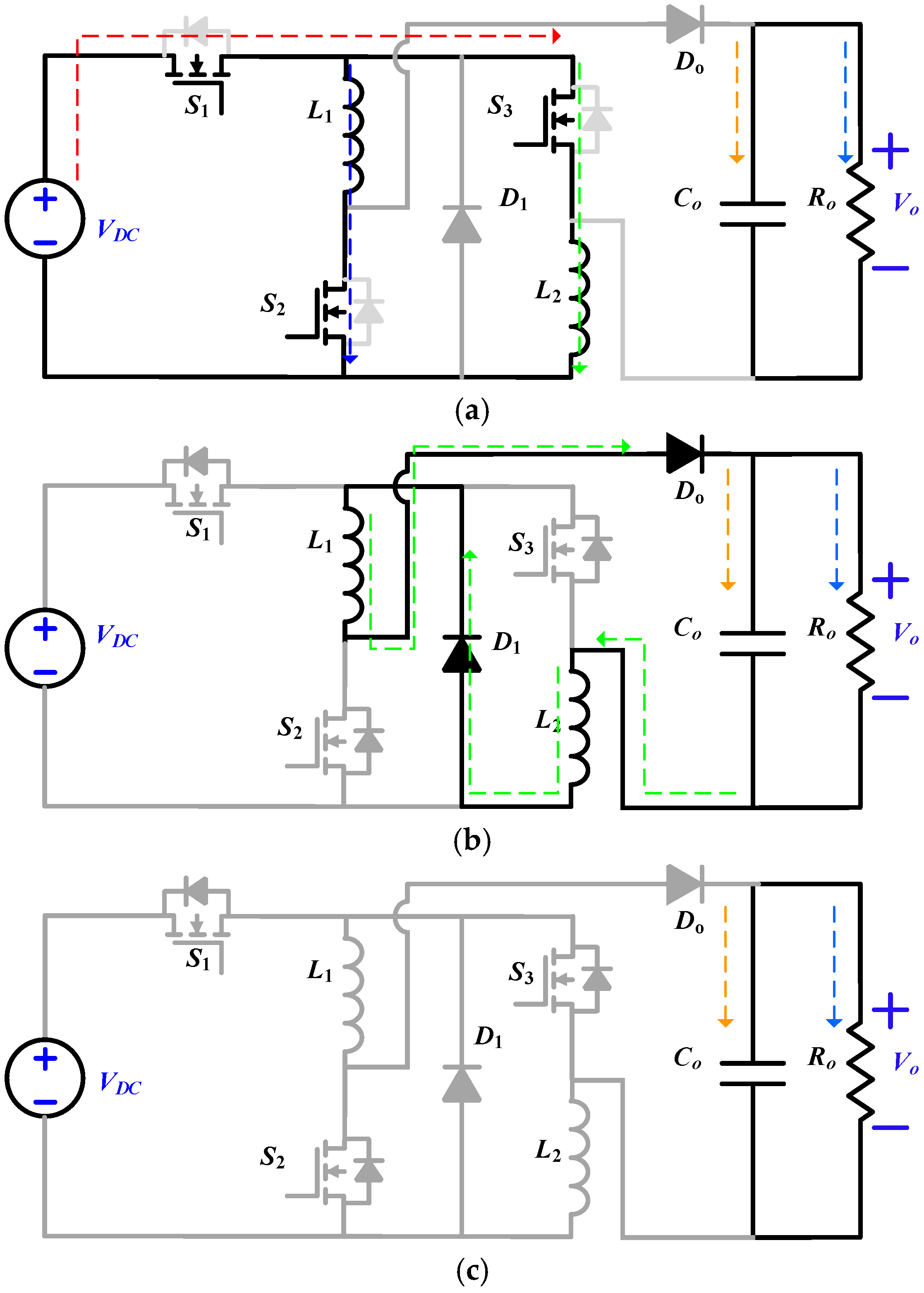
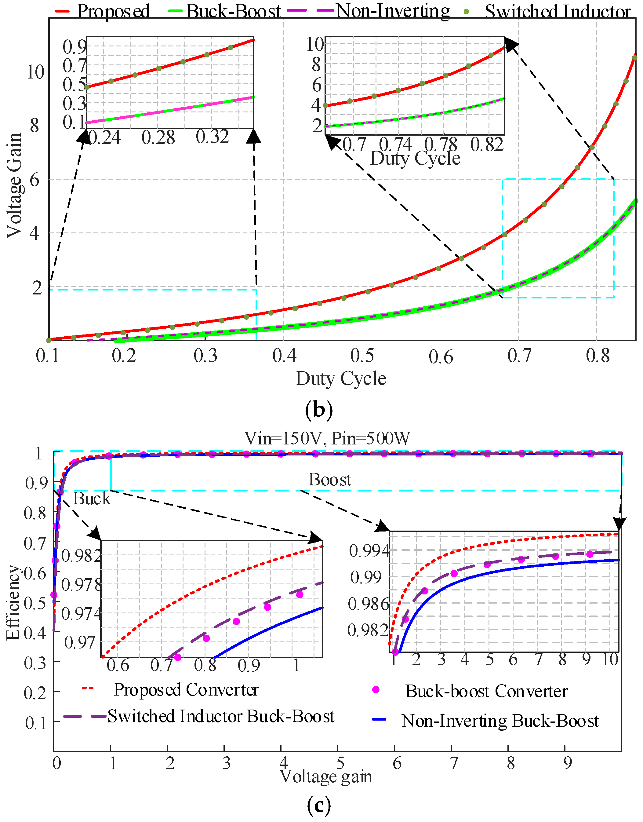
2. Proposed Buck-Boost Dc–Dc Converter

The configuration of the proposed buck-boost dc–dc converter is illustrated in Figure 1 [17]. The structure is implemented using three power switches (S1, S2, S3), two diodes (D1, Do), two inductors (L1, L2), and an output capacitor (Co). The three switches are triggered on and off simultaneously, and the diodes operate as freewheeling diodes. The two inductors charge in parallel and discharge in series.
The converter is able to operate in continuous conduction mode (CCM) and discontinuous conduction mode (DCM). Both modes of operation will be considered in the following sections.

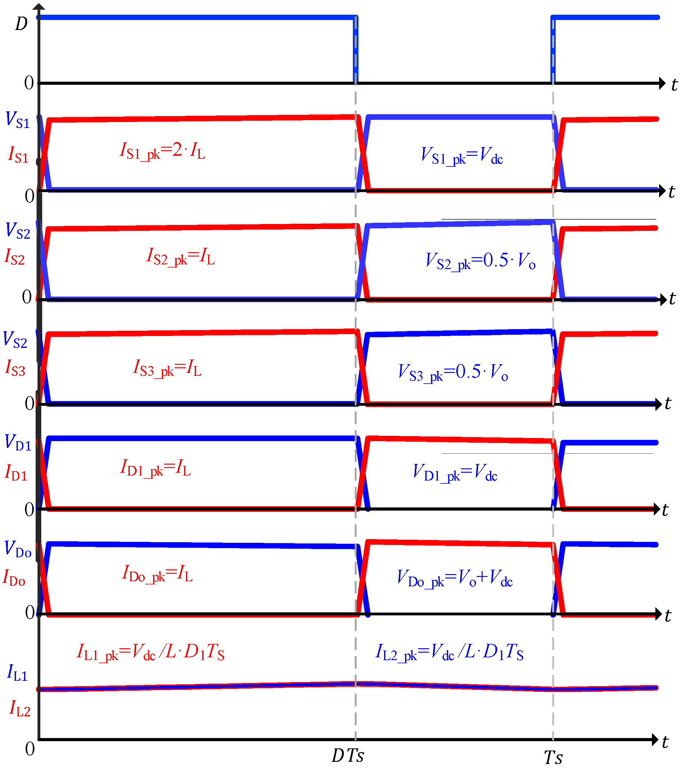
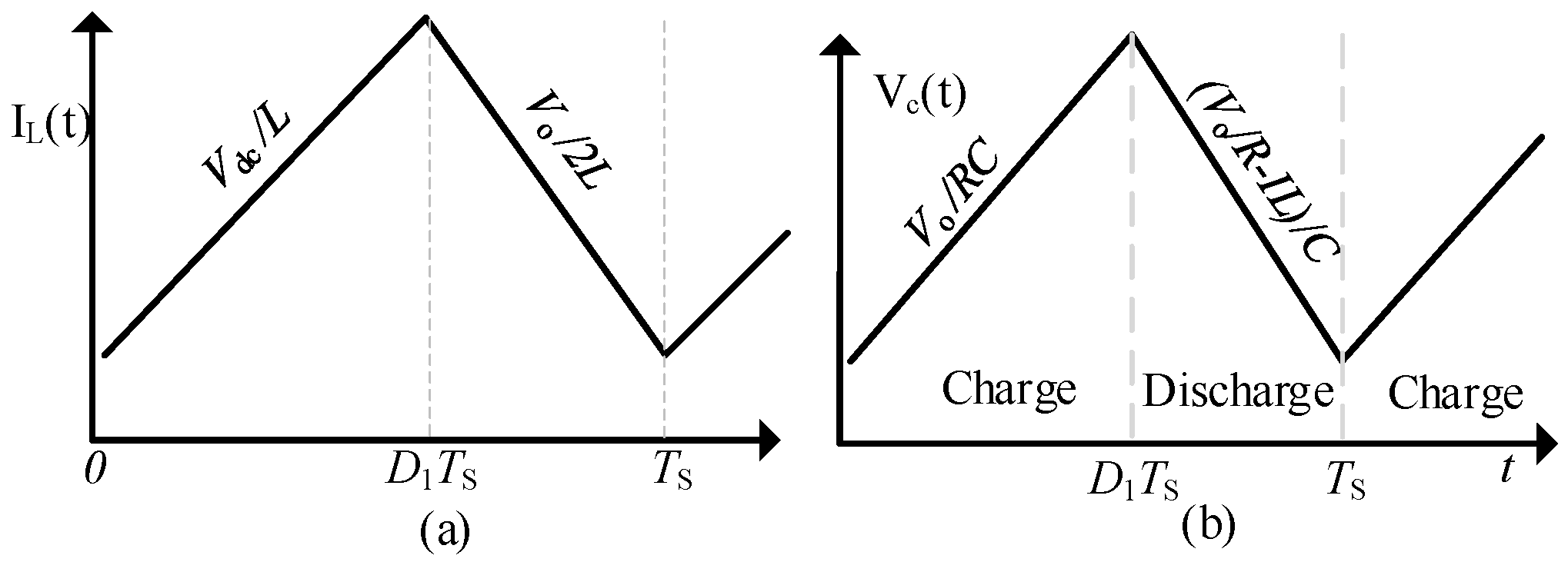
2.1. Continuous Conduction Mode

In order to simplify the analysis of the CCM mode, two assumptions are considered in the forthcoming analysis:
 
Capacitor voltage ripple is very small compared with the voltage itself, thus it could be neglected.
 
Inductor current ripple is negligible because of its very small value.
 
All semiconductor devices are ideal.
The converter power switches are triggered ON and OFF simultaneously, hence the converter will have two operating modes; see Figure 2a,b. Typical waveforms of the converter in CCM are shown in Figure 3.
Mode I [0-DTS]: In this time period, switches (S1, S2, S3) are turned ON, while diodes (D1, Do) are turned OFF. This mode is illustrated in Figure 2a. As can be seen from the figure, the two inductors charge in parallel from the source. Applying Kirchhoff voltage law (KVL) and Kirchhoff current law (KCL) to Figure 2a, the following equations are deduced:
v L 1 = v L 2 = V d c
i c = V o R
i d = 0
Mode II [DTS-TS]: In this time period, switches (S1, S2, S3) are turned OFF and, consequently, diodes (D1, Do) are turned ON to provide a freewheeling path for the current. This mode is illustrated in Figure 2b. As can be investigated from the figure, the two inductors discharge their energies to the load in series. Applying Kirchhoff voltage law (KVL) and Kirchhoff current law (KCL) to Figure 2b, the following equations are deduced:
v L = v L 1 = v L 2
2 v L = V o
i C = I L V o R
i d = I L
The steady-state voltage gain of the proposed converter could be deduced from the analysis of the two modes of operation by applying voltage second balance, and the voltage gain of the proposed converter is as follows:
V o V d c = M = 2 D ( 1 D )
where v L 1 , v L 2 , V d c , V o , I L , i C , i d , M , and D are inductor L1 voltage, inductor L2 voltage, input voltage, output voltage, inductor current, capacitor current, diode current, voltage gain, and duty cycle, respectively.

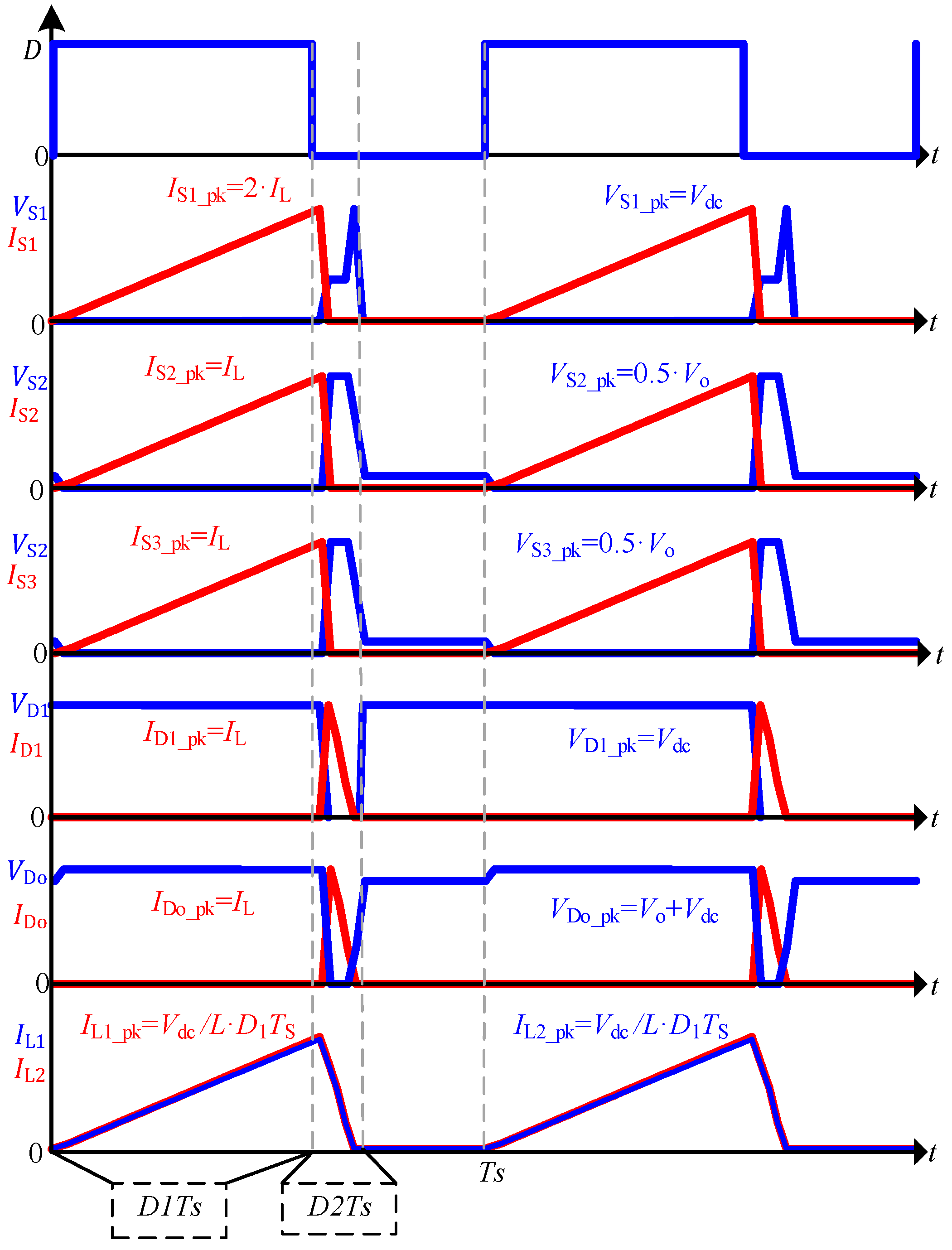
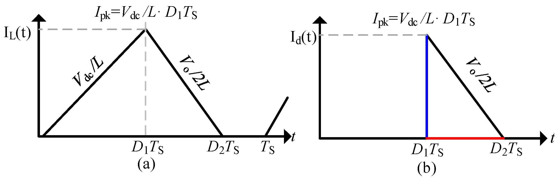
2.2. Discontinuous Conduction Mode

The discontinuous conduction mode typically occurs with large inductor current ripple in a converter operating at light load and containing current unidirectional switches. However, some converters are purposely designed to operate in DCM. The proposed converter will have three modes of operation while operating in DCM; see Figure 2a–c. The typical converter waveform while operating in DCM is illustrated in Figure 4.
Mode I and Mode II, which were discussed in the previous section, are similar to CCM analysis.
Mode III: In this interval, both the power switches and diodes are turned off. The inductors’ currents are zero, as illustrated in Figure 2c.
v L = 0
i C = V o R
i d = 0
Applying inductor volt-second balance in Equations (1), (5), and (9), the relation between input and output voltage is obtained:
D 1 v d c = D 2 v o
The duty cycle D2 is an unknown, so a second equation is needed to eliminate D2. Capacitor charge-balance is used to obtain the second equation. The average of the diode current is equal to the output current:
i d = V o R
A sketch of the inductor and diode currents in DCM is illustrated in Figure 5a,b. The dc component of the diode current is given by
i d = 1 T S 0 T S i d ( t ) d t
The peak diode current could be obtained from the graph as
i p k = V o 2 L D 1 T S
Solving Equations (13)–(15), the second required equation is obtained as
i d = 1 2 D 2 T S V o 2 L D 1 = V o R
Let
k = 2 L R T S
Then
D 2 = 2 k / D 1
Finally, the converter voltage gain in DCM operation is given as
V o V d c = M = D 1 2 ( 2 K )
where D 1 , D 2 , T S , and R0 are periods when the switches are conducting, periods when the diode is conducting, switching time, and load resistance, respectively.
The boundary for CCM and DC operation can be obtained by relating inductor current and inductor ripple
I L > Δ i L For   CCM
I L < Δ i L For   DCM
Substituting CCM solutions for I L and Δ i L in (20)
V d c R ( 2 D 1 D ) 2 > V d c 2 L D T S
Equation (22) could be rearranged to
2 L R T S = K > D ( 2 D 1 D ) 2
Hence
K c r i = D ( 2 D 1 D ) 2
where K c r i is the critical boundary between CCM and DCM.
According to the above analysis, the converter can operate on CCM or DCM based on the operating conditions; in order to avoid such conditions, accurate design of the converter must be considered. Figure 6 represents the boundary condition between CCM and DCM at different duty cycles and different power while the output voltage is fixed at 350 V.

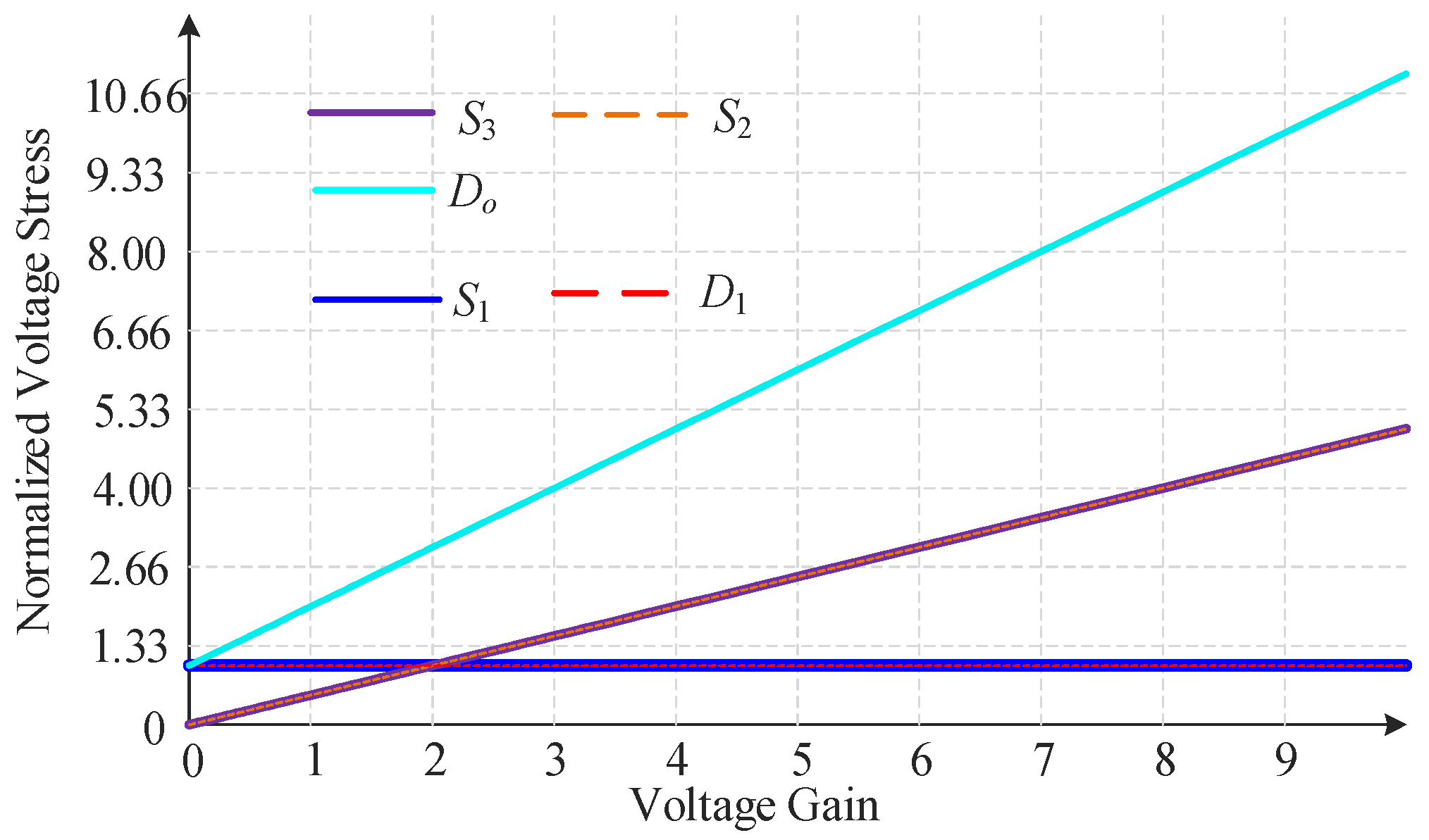
2.3. Switches’ and Diodes’ Voltage Stresses

Voltage and current stress are important parameters in designing and selecting circuit parameters, and the proposed converter switching elements’ stress is discussed below.
Switches S1, S2, and S3 are triggered in a simultaneous manner, but their ratings are different. The voltage stress of switch S1 is equal to
V d s S 1 = V d c
The current stress of switch S1 is given by
I S 1 = 2 I L
Switches S2 and S3 face similar voltage and current stress, as follows:
V d s S 2 = V d s S 3 = V o 2
I S 2 = I S 3 = I L
Diodes D1 and Do work as freewheeling diodes and are activated in complementary manners to the switches. The voltage and current stress of both diodes are given by
V d 1 = V d c
I d 1 = I L
V d o = V d c + V o
I S 2 = I L
A depiction of the devices’ normalized voltage stresses with different voltage gain is illustrated in Figure 7. In Figure 7, the voltage stress is normalized to the input voltage.

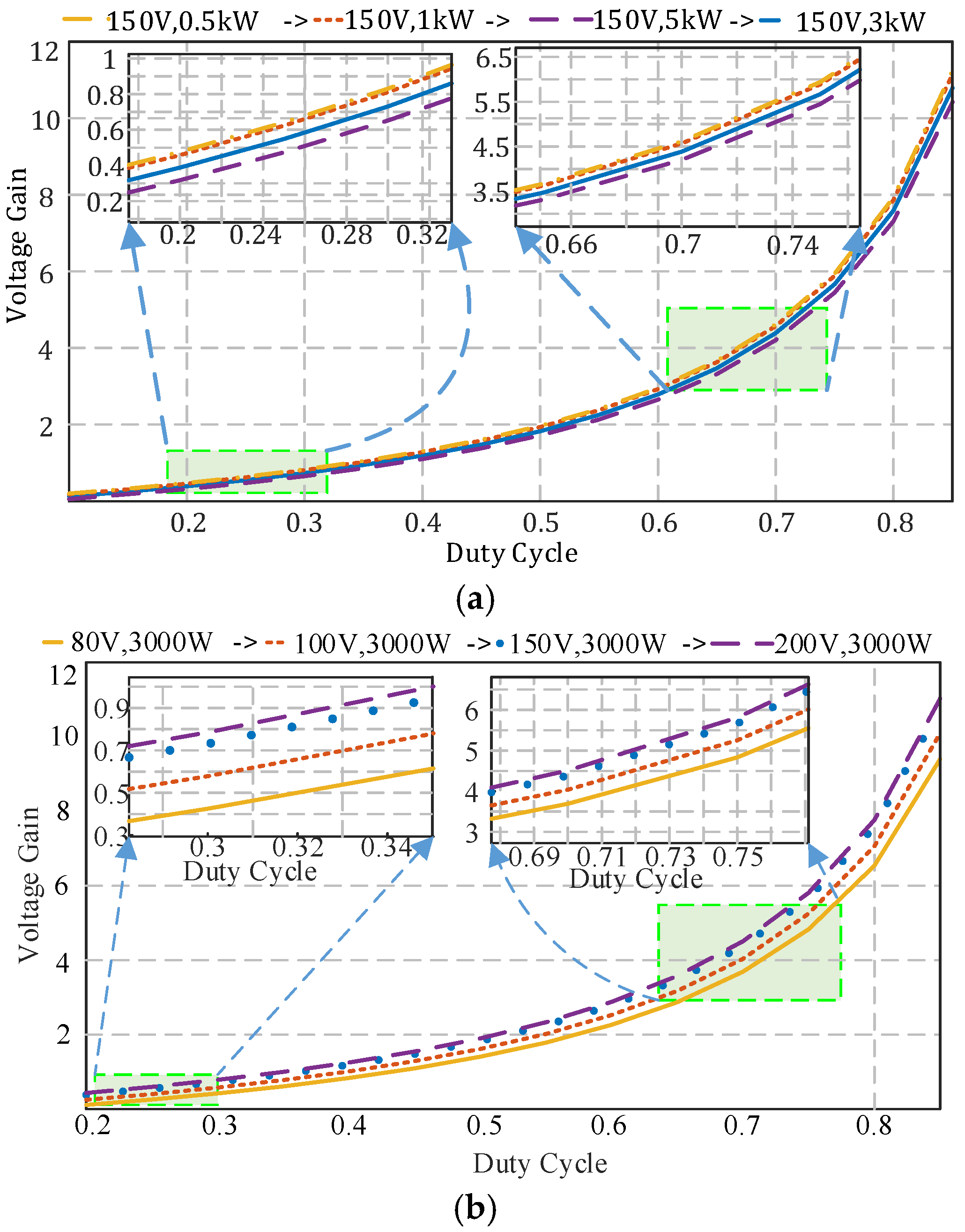
2.4. Components’ Design

The design of the circuit parameters, inductors, and capacitor is obtained from the steady-state analysis performed in the previous sections. Utilizing inductor volt-second balance and capacitor charge, the designs of parameters are as follows:

2.4.1. Inductors’ Design

Inductors’ selection is based on the required ripple of its current. The inductor current ripple in CCM is drawn in Figure 8a and is given by
Δ i L = Δ i L o n = Δ i L o f f = V d c D T S L = V o ( 1 D ) T S 2 L
This equation is valid in both CCM and DCM. By defining the required amount of ripple, the inductor value could be defined as follows:
L = ( V o ( 1 D ) ) T S ( 2 Δ i L )
Based on Equation (29), there is a dependency between inductance L and duty cycle D. In order to avoid any misoperation of the converter, we design the inductance based on the extreme condition that the current ripple at the extreme scenario does not exceed the required ripple and when duty cycle below the ripple will be below the required level.
Let us assume the required ripple Δ i L is 10%, then we can calculate L at the duty cycle around 0.82. Then, when the duty cycle is lower than 0.85, the ripple will be less than 10%.

2.4.2. Capacitors’ Design

The output capacitor value is selected based on the amount of voltage ripple acceptable in the output voltage. The output capacitor voltage waveform is illustrated in Figure 8b and the ripple equation is as follows:
Δ v = Δ v c o n = Δ v o o f f = ( V o I L ) ( 1 D ) T S R C = V o D T S R C
This equation is valid in both CCM and DCM. By defining the required amount of ripple, the capacitor value could be defined as follows:
C o = ( V o D T S ) ( Δ v R )
where Δ i L , Δ i L o n , Δ i L o f f , L , Δ v , Δ v c o n , Δ v o o f f , and C are inductor current ripple, inductor ripple while the inductor is charging, inductor ripple while the inductor is discharging, inductor value, capacitor ripple, capacitor ripple while the capacitor is charging, capacitor ripple while the capacitor is discharging, and capacitor value, respectively.
Based on Equation (30), there is a dependency between capacitance C and duty cycle D. In order to avoid any misoperation of the converter, we design the capacitance based on the extreme condition that the voltage ripple at the extreme scenario does not exceed the required ripple and when duty cycle below the ripple will be below the required level
Let us assume the required ripple Δ v is 10%, then we can calculate C at the duty cycle around 0.82. Then, when the duty cycle is lower than 0.85, the ripple will be less than 10%.

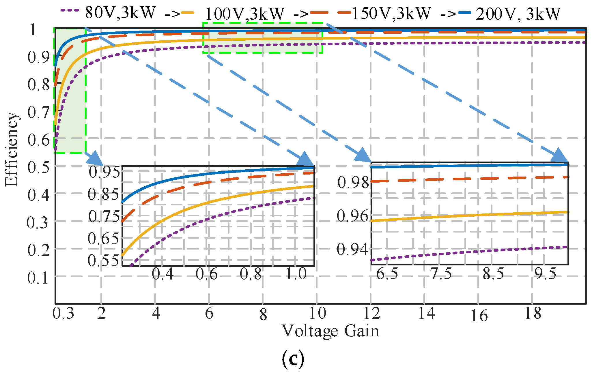
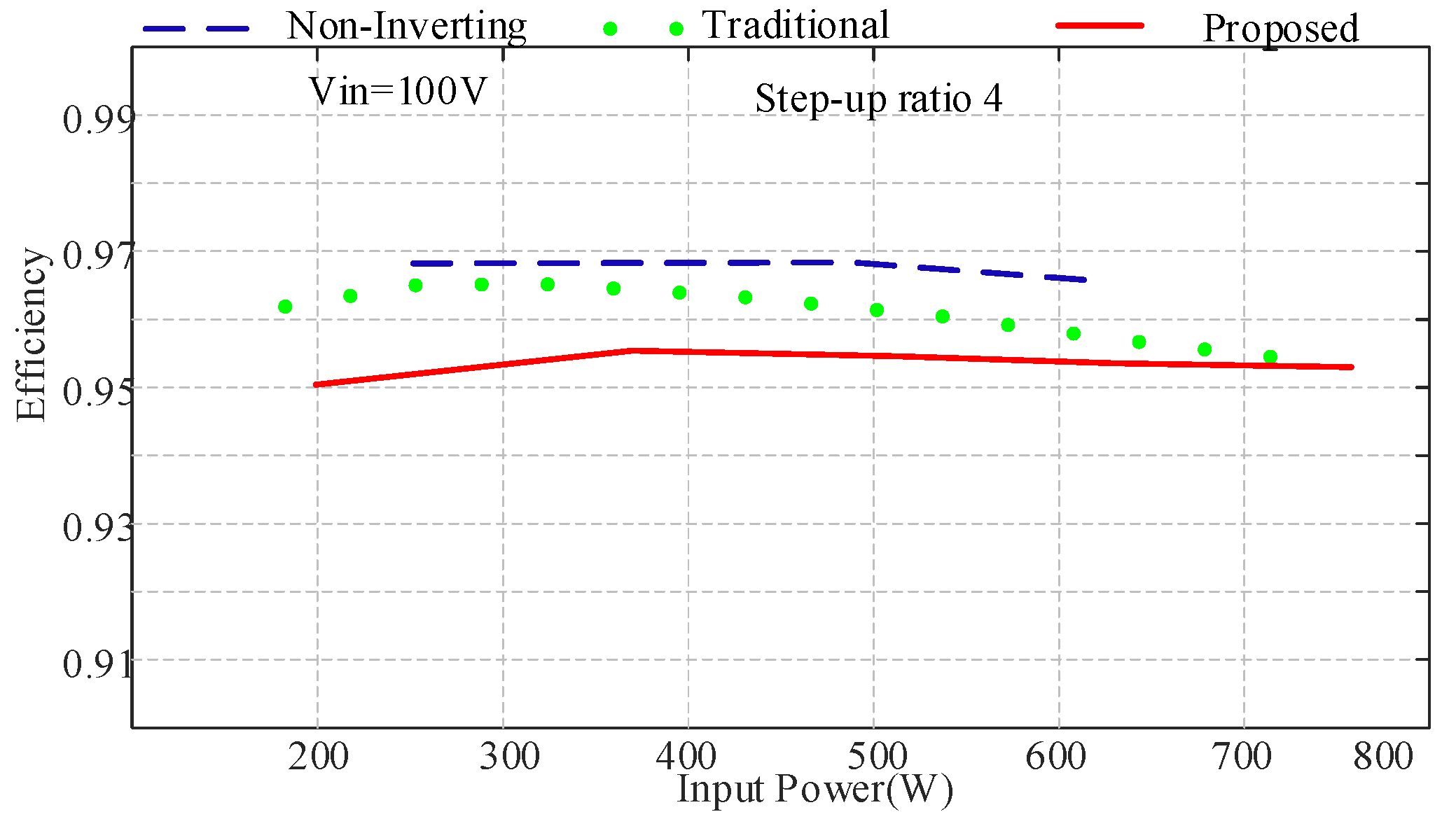
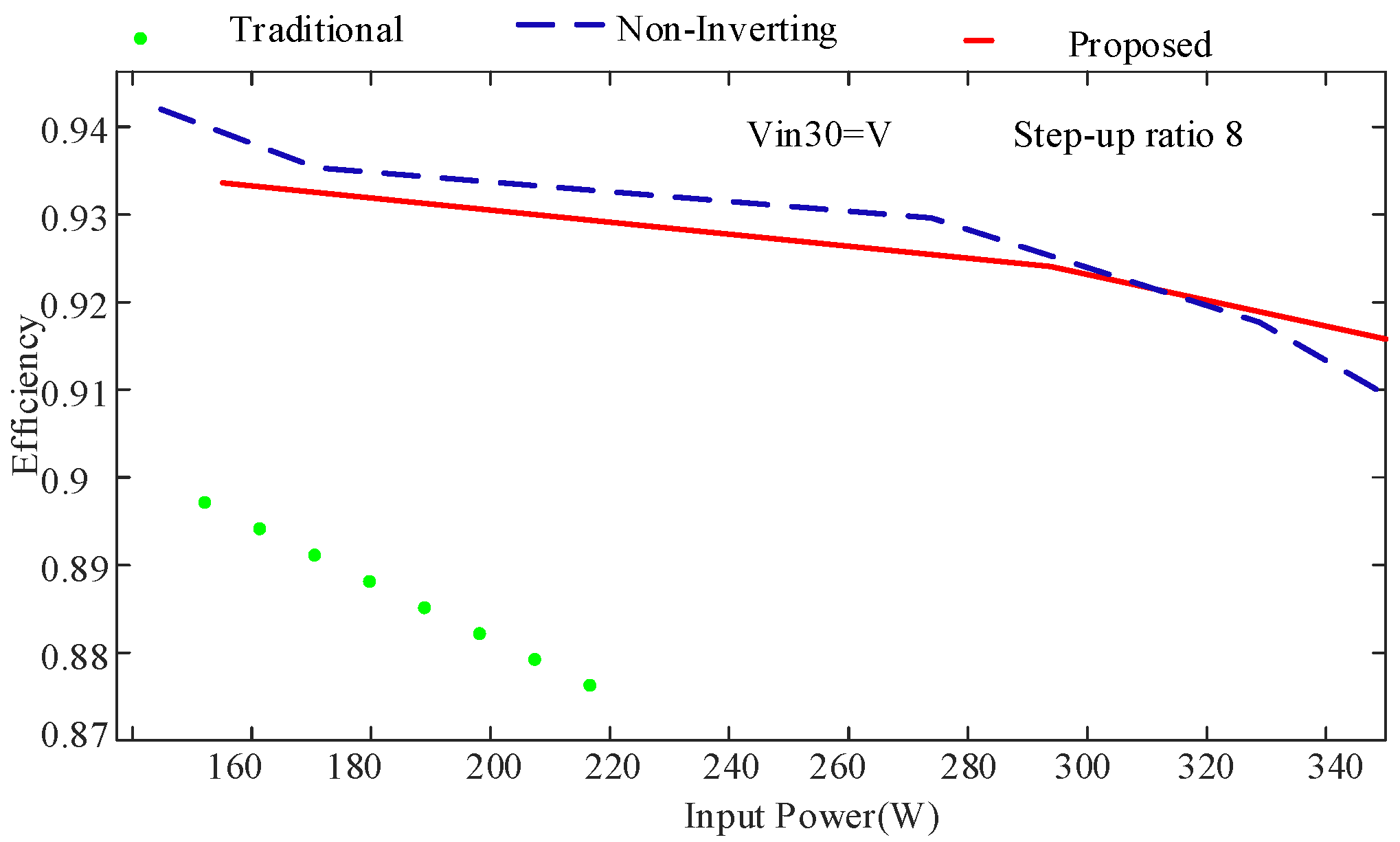
2.4.3. Comparative Study

Converter performance mainly depends on the input voltage, input power, and step-up ratio. The converter voltage gain is affected by the loading profile and supply voltage. In Figure 9a, the input voltage is fixed at 150 V, while different loading profiles are applied; at light load, the converter conversion ability is higher than at heavy loading. The second case study is illustrated in Figure 9b, where load profile is fixed with different supply voltages; as the supply voltage increases, the step-up/-down ability increases.
However, in both case studies, the differences in the voltage gain do not have a very high ratio.
Converter efficiency depends on many factors such as the load profile, source voltage, and voltage gain. In the scenario illustrated in Figure 9c, the load profile is fixed while both voltage gain and source voltage are variable. In buck mode, as the source voltage increases and the bucking ratio is lowered, the converter demonstrates the highest efficiency, while with lower input voltage and a higher bucking ratio, the converter efficiency is low. During boosting mode, as source voltage increases, efficiency increases too.
Another case study is considered in Figure 10a, where input voltage is set to 150 V, while load profile is variable and efficiency is measured at different voltage gains. With heavy loading, the converter demonstrates lower efficiency than with a medium or moderate loading profile. A comparison between the proposed converter and different converters reported in the literature is illustrated in Table 1. In the voltage gain comparison illustrated in Figure 10b, both the proposed converter and switched inductor buck-boost converter have similar step-up/-down ability, but the proposed converter has higher efficiency; see Figure 10c.

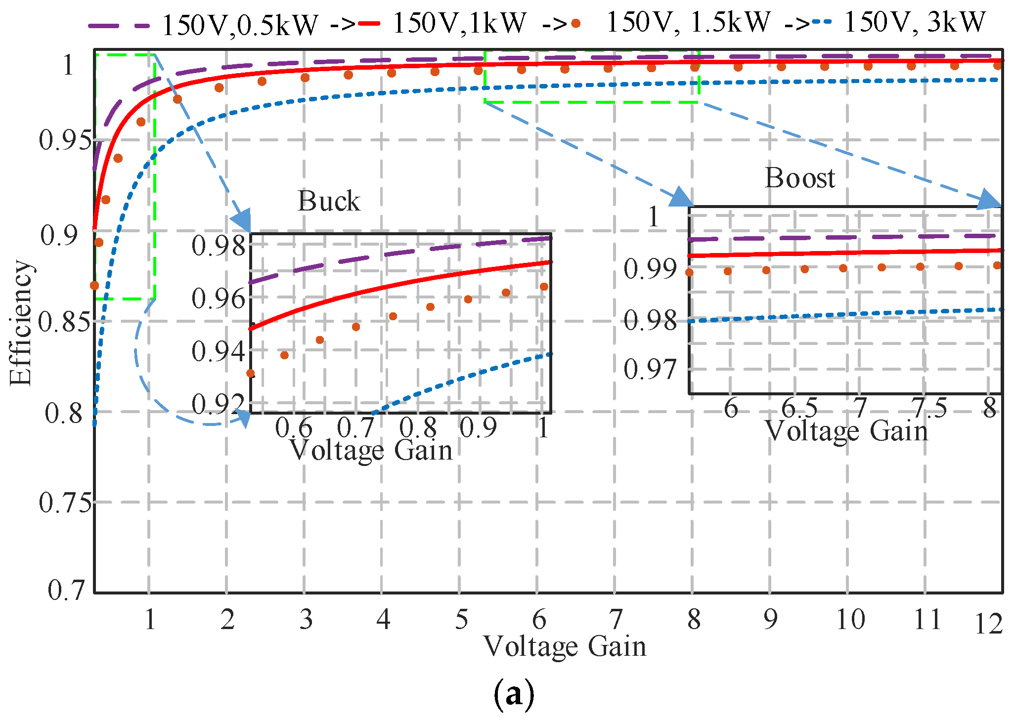
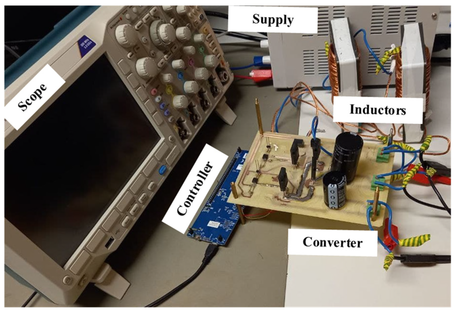
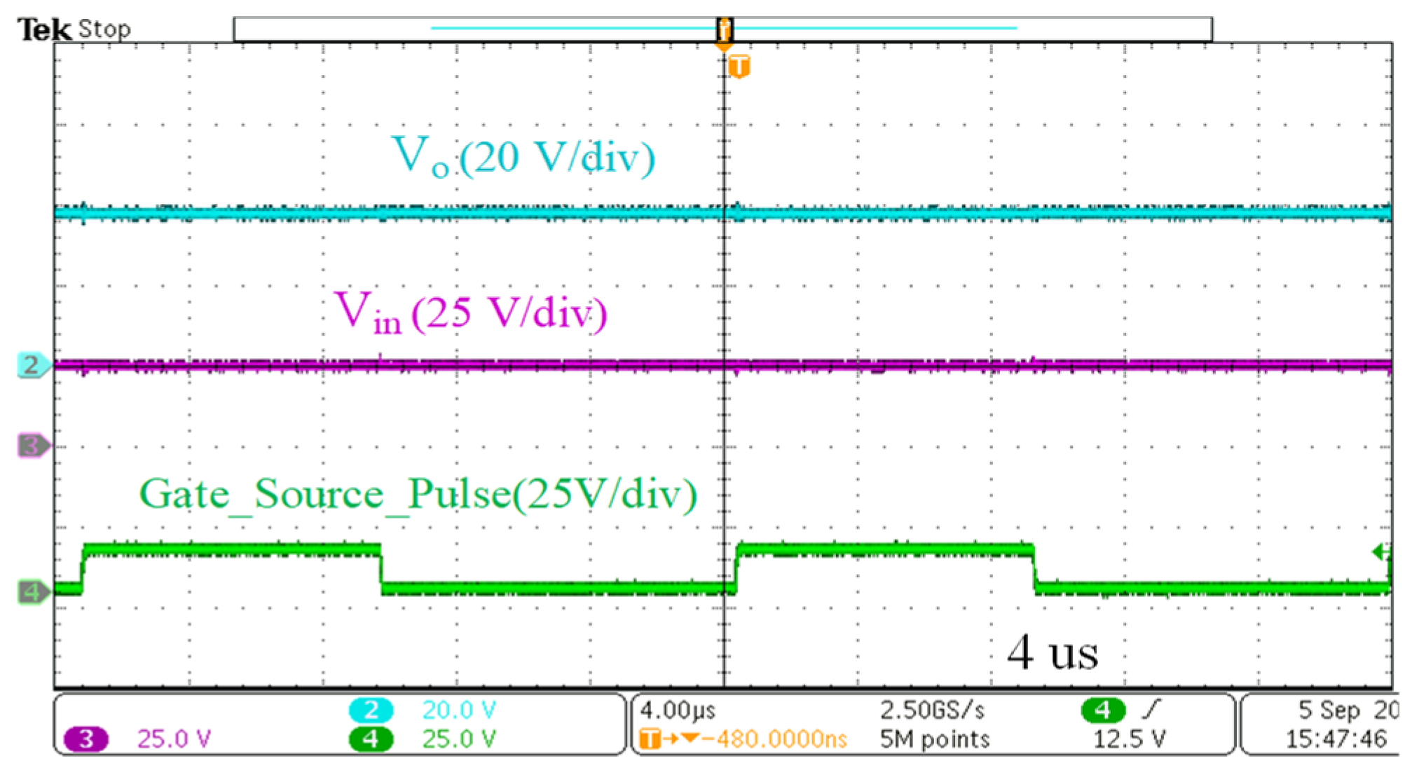
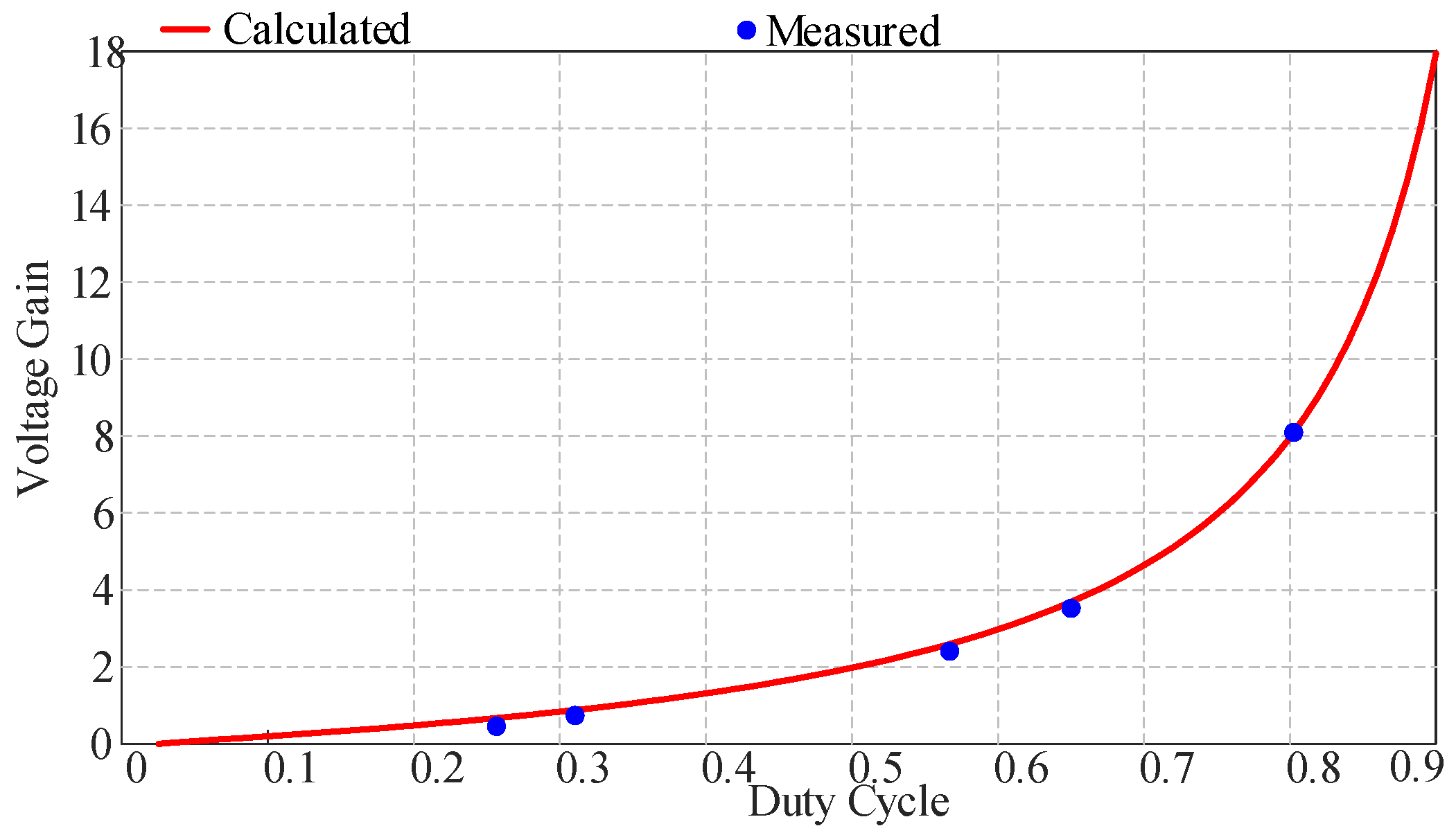
3. Experimental Verification

This section provides the experimental results of the developed system, and the parameters used to build the prototype are illustrated in Table 2. A photo of the proposed system is shown in Figure 11.
A case study where the duty cycle is set to 0.6 with 30 V input voltage is illustrated in Figure 12. Three switches are operating in synchronous manner, hence the gate source pulses for the three switches are the same as illustrated in Figure 12a. Diodes D1 and Do are operating as freewheeling diodes. The cathode–anode voltages of the two diodes are illustrated in Figure 12b. The input current is the sum of the two inductors’ currents when the switches are on and zero when the switches are off, and the input capacitor smoothens the input current. The drain source voltages of the three switches are illustrated in Figure 12c. Switches S2 and S3 face the same voltage stress and carry the same current.
Figure 12d illustrates switch S1 current, which is equal to the sum of the two inductors’ currents. Switch S2 current is illustrated in Figure 12e, which is equal to the inductor current. The output diode current is illustrated in Figure 12f, where spikes are noted in the switches and diode currents because of a problem in the used probe; however, it does not exist in real current as there are no spikes in the measured voltages.
A boosting case study is considered in Figure 13, where the input voltage is 25 V and the output voltage generated is around 38 V, and a bucking case study is illustrated in Figure 14, where the input voltage is 23 V, output voltage is 9.25 V, duty cycle is 0.2244, and voltage gain is 0.4.
The converter voltage gain was measured experimentally, and the theoretical and measured voltage gains of the converter with varying duty cycles are illustrated in Figure 15. For comparison purposes, three prototypes were built in the laboratory for the traditional buck-boost, non-inverting buck-boost, and proposed converter. The three prototypes were built using the same parameters as in Table 2. In the first case study, which is illustrated in Figure 16, the input voltage is set to 100 V and the step ratio is fixed at 3.7. For such a step-up ratio, the proposed converter requires a duty cycle of 0.68, while the conventional and non-inverting buck-boost converters both require a duty cycle of 0.8.
In this case study, the non-inverting converter demonstrates the highest efficiency, while at high power, both the proposed and conventional converter have the same efficiency. In the second case study, which is illustrated in Figure 17, the input voltage is fixed at 30 V and the step-up ratio is 8. The efficiency of the proposed converter and the non-inverting converter is comparable, but with the increase in power (over 300 W), the proposed converter demonstrates the highest efficiency.
The last case study demonstrates step-down comparison. In Figure 18, the input voltage is fixed at 150 V and the step-down ratio is 3. The non-inverting converter demonstrates the lowest efficiency. The proposed converter and the conventional converter demonstrate comparable efficiency at low power, but with the increase in input power, the proposed converter demonstrates the highest efficiency.

4. Conclusions

In this paper, a new non-inverting high-gain buck-boost structure is developed with improved step-up/-down ability. The performance of the converter in both CCM and DCM is studied and analyzed. The design of the converter elements is investigated and described. The operating conditions and voltage/current stress of each device are studied. Based on the performed analysis, the proposed converter devices are under low voltage and current stress compared with other buck-boost converters. A 700 W prototype was built for the converter to investigate its performance experimentally. The efficiency of the proposed converter is measured at different voltage gains and compared with the traditional buck-boost converter.
The theoretical and measured voltage gain matched. While working in step-up, the converter demonstrated better performance at high power. The peak measured efficiency of the converter at a step-up ratio of 3.7 was 95.4%.

Author Contributions

O.A.-R. developed and simulated the idea; O.A.-R., A.C. and A.B. implemented the idea prototype and verified the experimental results; O.A.-R. and D.V. revised the data and results; O.A.-R. wrote the first draft; O.A.-R., D.V. and D.P. revised the manuscript. All authors have read and agreed to the published version of the manuscript.

Funding

This research was financed in part by the European Economic Area (EEA) and Norway Financial Mechanism 2014–2021 under Grant EMP474 and in part by the Estonian Research Council under Grant PRG1086 and the programme Mobilitas Pluss (Grant MOBJD1033).

Conflicts of Interest

The authors declare no conflict of interest.

References

  1. Abdel-Rahim, O.; Chub, A.; Blinov, A.; Vinnikov, D. Buck-Boost Resonant Z-Source Parital Power Converter. In Proceedings of the 2022 3rd International Conference on Smart Grid and Renewable Energy (SGRE), Doha, Qatar, 20–22 March 2022; pp. 1–6. [Google Scholar] [CrossRef]
  2. Abdel-Rahim, O.; Orabi, M.; Ahmed, M.E. Buck-Boost Interleaved Inverter For Grid Connected Photovoltaic System. In Proceedings of the 2010 IEEE International Conference on Power and Energy, Kuala Lumpur, Malaysia, 29 November–1 December 2010; pp. 63–68. [Google Scholar] [CrossRef]
  3. Callegaro, L.; Ciobotaru, M.; Fletcher, J.E. An Intelligent Pass-Through Algorithm for Non-Inverting Buck-Boost Solar Power Optimizers. In Proceedings of the 2019 21st European Conference on Power Electronics and Applications (EPE ’19 ECCE Europe), Genova, Italy, 3–5 September 2019; pp. P.1–P.10. [Google Scholar] [CrossRef]
  4. Linares, L.; Erickson, R.W.; MacAlpine, S.; Brandemuehl, M. Improved Energy Capture in Series String Photovoltaics via Smart Distributed Power Electronics. In Proceedings of the 2009 Twenty-Fourth Annual IEEE Applied Power Electronics Conference and Exposition, Washington, DC, USA, 15–19 February 2009; pp. 904–910. [Google Scholar] [CrossRef]
  5. Abdel-Rahim, O.; Orabi, M.; Ahmed, M.E. High Gain Single-Stage Inverter For Photovoltaic AC Modules. In Proceedings of the 2011 Twenty-Sixth Annual IEEE Applied Power Electronics Conference and Exposition (APEC), Fort Worth, TX, USA, 6–11 March 2011; pp. 1961–1967. [Google Scholar] [CrossRef]
  6. Banaei, M.R.; Bonab, H.A.F. A High Efficiency Nonisolated Buck–Boost Converter Based on ZETA Converter. IEEE Trans. Ind. Electron. 2019, 67, 1991–1998. [Google Scholar] [CrossRef]
  7. Banaei, M.R.; Bonab, H.A.F. A novel structure for single-switch nonisolated transformerless buck–boost DC–DC con-verte. IEEE Trans. Ind. Electron. 2016, 64, 198–205. [Google Scholar] [CrossRef]
  8. Ajami, A.; Ardi, H.; Farakhor, A. Design, analysis and implementation of a buck–boost DC/DC converter. IET Power Electron. 2014, 7, 2902–2913. [Google Scholar] [CrossRef]
  9. Son, H.-S.; Kim, J.-K.; Lee, J.-B.; Moon, S.-S.; Park, J.-H.; Lee, S.-H. A New Buck–Boost Converter With Low-Voltage Stress and Reduced Conducting Components. IEEE Trans. Ind. Electron. 2017, 64, 7030–7038. [Google Scholar] [CrossRef]
  10. Abdel-Rahim, O.; Furiato, H. Switched Inductor Quadratic Boosting Ratio Inverter With Proportional Resonant Controller For Grid-Tie PV Applications. In Proceedings of the IECON 2014—40th Annual Conference of the IEEE Industrial Electronics Society, Dallas, TX, USA, 29 October–1 November 2014; pp. 5606–5611. [Google Scholar] [CrossRef]
  11. Maldonado, J.C.M.; Valdez-Resendiz, J.E.E.; Vite, P.M.G.; Rosas-Caro, J.C.; Rivera-Espinosa, M.D.R.; Valderrabano-Gonzalez, A. Quadratic Buck–Boost Converter with Zero Output Voltage Ripple at a Selectable Operating Point. IEEE Trans. Ind. Appl. 2019, 55, 2813–2822. [Google Scholar] [CrossRef]
  12. Rosas-Caro, J.C.; Valdez-Resendiz, J.E.; Mayo-Maldonado, J.C.; Alejo-Reyes, A.; Valderrabano-Gonzalez, A. Quadratic buck–boost converter with positive output voltage and minimum ripple point design. IET Power Electron. 2018, 11, 1306–1313. [Google Scholar] [CrossRef]
  13. Nousiainen, L.; Suntio, T. Dynamic characteristics of current-fed semi-quadratic buck-boost converter in photovoltaic applications. In Proceedings of the 2011 IEEE Energy Conversion Congress and Exposition, Phoenix, AZ, USA, 17–22 September 2011; pp. 1031–1038. [Google Scholar] [CrossRef]
  14. Yari, K.; Shahalami, S.H.; Mojallali, H. A Novel Nonisolated Buck–Boost Converter with Continuous Input Current and Semiquadratic Voltage Gain. IEEE J. Emerg. Sel. Top. Power Electron. 2021, 9, 6124–6138. [Google Scholar] [CrossRef]
  15. Yari, K.; Mojallali, H.; Shahalami, S.H. A New Coupled-Inductor-Based Buck–Boost DC–DC Converter for PV Applications. IEEE Trans. Power Electron. 2021, 37, 687–699. [Google Scholar] [CrossRef]
  16. AL-Hakeem, K.M.; Ahmad, O.A. Buck-Boost In-Out of Phase Y-source AC Matrix Converter. In Proceedings of the 2018 Third Scientific Conference of Electrical Engineering (SCEE), Baghdad, Iraq, 19–20 December 2018; pp. 274–279. [Google Scholar] [CrossRef]
  17. Abdel-Rahim, O.; Chub, A.; Blinov, A.; Vinnikov, D. New High-Gain Non-Inverting Buck-Boost Converter. In Proceedings of the IECON 2021—47th Annual Conference of the IEEE Industrial Electronics Society, Toronto, ON, Canada, 13–16 October 2021; pp. 1–6. [Google Scholar] [CrossRef]
  18. Smedley, K.; Cuk, S. Dynamics of one-cycle controlled Cuk converters. IEEE Trans. Power Electron. 1995, 10, 634–639. [Google Scholar] [CrossRef] [Green Version]
  19. Ericson, R.; Maksimovic, D. Fundamentals of Power Electronics; Kluwer Academic Publishers: Dordrecht, The Netherlands, 2007. [Google Scholar]
  20. Abdel-Rahim, O.; Orabi, M.; Abdelkarim, E.; Ahmed, M.; Youssef, M.Z. Switched Inductor Boost Converter For PV Applications. In Proceedings of the 2012 Twenty-Seventh Annual IEEE Applied Power Electronics Conference and Exposition (APEC), Orlando, FL, USA, 5–9 February 2012; pp. 2100–2106. [Google Scholar] [CrossRef]
  21. Lakshmi, M.; Hemamalini, S. Nonisolated High Gain DC–DC Converter for DC Microgrids. IEEE Trans. Ind. Electron. 2017, 65, 1205–1212. [Google Scholar] [CrossRef]
  22. Sarikhani, A.; Allahverdinejad, B.; Hamzeh, M. A Nonisolated Buck–Boost DC–DC Converter with Continuous Input Current for Photovoltaic Applications. IEEE J. Emerg. Sel. Top. Power Electron. 2020, 9, 804–811. [Google Scholar] [CrossRef]
  23. Miao, S.; Wang, F.; Ma, X. A New Transformerless Buck–Boost Converter with Positive Output Voltage. IEEE Trans. Ind. Electron. 2016, 63, 2965–2975. [Google Scholar] [CrossRef]
Figure 1. Proposed buck-boost dc–dc converter.
Energies 15 04550 g001
Figure 2. Operation modes of the proposed converter: (a) operation mode #1, (b) operation mode #2, and (c) operation mode #3.
Energies 15 04550 g002
Figure 3. Typical converter waveforms in CCM.
Energies 15 04550 g003
Figure 4. Typical converter waveforms in DCM.
Energies 15 04550 g004
Figure 5. DCM operation (a) inductor current and (b) diode current.
Energies 15 04550 g005
Figure 6. CCM and DC boundary.
Energies 15 04550 g006
Figure 7. Circuit component voltage stress normalized to input voltage vs. converter voltage gain.
Energies 15 04550 g007
Figure 8. CCM operation (a) inductor current and (b) output capacitor voltage.
Energies 15 04550 g008
Figure 9. Different cases of study for the proposed converter: (a) Voltage gain at different duty cycle and different loading. (b) Voltage gain with fixed loading and different input voltages. (c) Converter efficiency at different input voltages.
Energies 15 04550 g009aEnergies 15 04550 g009b
Figure 10. (a) Converter efficiency at fixed input voltage and different loading, (b) voltage gain comparison among the proposed and other buck-boost converters, and (c) efficiency comparison among the proposed and other buck-boost converters.
Energies 15 04550 g010aEnergies 15 04550 g010b
Figure 11. Experimental set-up schematic.
Energies 15 04550 g011
Figure 12. Experimental results of converter at duty cycle of 0.6 and input voltage of 30 V: (a) gate source pulses; (b) Ch1 diode D1 voltage, diode Do voltage, and input current; (c) Ch1 output diode Do voltage, Ch3 switches’ S2 and S3 voltage, and Ch2 inductor L1 current; (d) Ch1 switch S3 voltage; Ch2 switch S3 currents; (e) Ch2 switch S2 voltage, Ch3 switch S2 current, and inductor current; and (f) Ch2 diode Do voltage and diode Do current.
Energies 15 04550 g012
Figure 13. Boosting case study, where the input voltage is 25 V, output voltage is 38 V, duty cycle is 0.428, and voltage gain is 1.52.
Energies 15 04550 g013
Figure 14. Bucking case study, where the input voltage is 23 V, output voltage is 9.25 V, duty cycle is 0.2244, and voltage gain is 0.4.
Energies 15 04550 g014
Figure 15. Calculated and measured converter voltage gain vs. duty cycle.
Energies 15 04550 g015
Figure 16. Measured efficiency comparison between the proposed converter, non-inverting buck-boost, and traditional buck-boost converter at a step-up ratio of 3.7.
Energies 15 04550 g016
Figure 17. Measured efficiency comparison between the proposed, non-inverting, and traditional buck-boost converter at a step-up ratio of 8.
Energies 15 04550 g017
Figure 18. Measured efficiency comparison between the proposed, non-inverting buck-boost, and traditional buck-boost converter at a step-down ratio of 3.
Energies 15 04550 g018
Table 1. Voltage gain and component stress comparison.
Converter
Topology
Gain
M = Vo/Vin
Components’ CountSwitches’ and Diodes’ Voltage StressSwitches’ and Diodes’ Current Stress
SwitchDiodeLC
Buck-Boost [18](D/(1-D))1111S:VoIL
D:(Vo+Vin)IL
Non-Inverting [19](D/(1-D))2211S1:VinIL
S2:VoIL
D1:VinIL
Do:VoIL
Cuk [5](D/(1-D))1221S1:Vin/(1-D)IL
D1:VinIL
Do:VoIL
SEPIC [19](D/(1-D))1122S1:Vo+Vin2IL
D1:Vo+VinIL
SIBBC [20]2D/(1-D)1421S1:Vo+Vin2IL
D1:VinIL
D2:Vo/2IL
D3:Vo/2IL
Do:Vo+VinIL
Lakshmi [21](1+D1)/(1-D1-D2)3221S1:(Vo+Vin)/2IL
S2:(Vo+Vin)/2IL
S3:VoIL
D1:VoIL
Do:Vo+VinIL
[22]2D/(1-D)22323S1:1/(1-D)*VinIL
S2:Vin *(1+D)/(1-D)2IL
D1:Vin/(1-D)IL
D2:Vin/(1-D)IL
Do:Vo+Vin/(1-D)IL
[23]D2/(1-D)22222S1:1/(1-D)*Vin2IL
S2:Vin *D/(1-D)2IL
D1:Vin/(1-D)IL
D2:Vin*D/(1-D)2IL
Proposed2D/(1-D)3221S1:Vin2IL
S2:Vo/2IL
S3:Vo/2IL
D1:VinIL
Do:Vo+VinIL
Table 2. Hardware prototype specifications.
ParameterValue
Input voltage range [V]33–150
P [W]700 W
Fs Switching Frequency30 kHz
Switches S1, S2, S3IMZ120R030M1HXKSA1
Diodes D1, DoDPG10I300PA
Inductors L1 = L21 mH
Capacitor Co320 µF
Publisher’s Note: MDPI stays neutral with regard to jurisdictional claims in published maps and institutional affiliations.

