Article

Accurate Circuit-Level Modelling of IGBTs with Thermal Phenomena Taken into Account

Department of Marine Electronics, Gdynia Maritime University, Morska 83, 81-225 Gdynia, Poland
*
Author to whom correspondence should be addressed.
Energies 2021, 14(9), 2372; https://doi.org/10.3390/en14092372
Submission received: 19 March 2021 / Revised: 16 April 2021 / Accepted: 20 April 2021 / Published: 22 April 2021
(This article belongs to the Special Issue Latest Advances in Electrothermal Models II)

Abstract

:
This paper proposes a new compact electrothermal model of the Insulated Gate Bipolar Transistors (IGBT) dedicated for SPICE (Simulation Program with Integrated Circuit Emphasis). This model makes it possible to compute the non-isothermal DC characteristics of the considered transistor and the waveforms of terminal voltages and currents of the investigated device and its internal temperature at transients. This model takes into account the nonlinearity of thermal phenomena in this device. The form of the formulated model is described and the problem of estimating its parameter values is discussed. The correctness of the proposed model was verified experimentally both at DC operation and at transients. The obtained results are compared to the results of computations performed with the use of the classical literature model. A very good agreement between the results of measurements and computations performed with the new model is obtained at different cooling conditions and in a wide range of changes of parameters characterising the electrical excitation of the tested device.

1. Introduction

IGBTs (Insulated Gate Bipolar Transistors) [1] are popular, fully voltage-controlled power semiconductor devices which make it possible to switch voltages and currents of high values [2]. They are used in such power converters as inverters [3,4,5] or DC-DC converters [6,7,8]. During operation of the considered transistors, their internal temperature increases as a result of self-heating phenomena [9,10,11,12,13]. An increase in this temperature causes shortening of the device life-time [13,14,15,16] and changes in the course of their characteristics [17,18,19].
Computer simulations are an important part of the process of designing electronic circuits. It can be realised e.g., in SPICE (Simulation Program with Integrated Circuit Emphasis) [9,20,21,22] or PLECS (Piecewise Linear Electrical Circuit Simulation) [23], which are the most popular tools to simulate power electronic networks [24,25,26,27]. Accuracy of the performed simulations depends on accuracy of the applied models of all components of the analysed network. Unfortunately, models of IGBTs built-in in popular simulation programmes are characterised by low accuracy [19,28]. In turn, as is shown in the cited papers the literature models often do not take into account the influence of such essential physical phenomena such as, e.g., self-heating or the sub-threshold effect [11,28,29,30,31,32,33,34,35,36,37], which can influence the shape of both dc and dynamic characteristics of an IGBT in an essential manner [19].
In the literature, a lot of IGBTs models of different accuracy can be found. Such models belong to one of the following groups: detailed models [38,39] or compact models [12,17,18,31]. Detailed models make it possible to obtain higher accuracy of computations of space-time distribution of, e.g., current density in the considered device can be computed with these models. Such a kind of model is especially dedicated to designers of semiconductor devices. Unfortunately, a high level of complexity of such models causes problems connected with the convergence of the computer analysis of electronic networks with many semiconductor devices [16]. Such analyses are very time consuming. Therefore, compact models [40,41,42,43,44] of semiconductor devices are commonly used in the analysis of electronic networks. Such models contain equations describing dependences between voltages and currents of these devices.
In order to take into account self-heating phenomena in the computer analyses, electrothermal models should be used [17,18]. In the analysis of electronic circuits, compact models are universally used. Compact electrothermal models make it possible to compute not only voltages and currents in the network, but also internal temperatures of semiconductor devices.
Models of the considered transistors of different accuracy and dedicated to different simulation environments are widely described in the literature. The review of some of these models is presented in the paper [19]. Each of the models described in the literature is dedicated to specific applications, but there is no universal model that takes into account all the essential physical phenomena occurring in the IGBT.
To formulate such a model, the classical network representation of the IGBT shown in Figure 1 is used. In this circuit a connection of the MOS transistor (MOS), the bipolar transistor (BJT) and the p-n diode (D) is visible [1,26].
In the paper [45] it is shown that for the structure in Figure 1, two dies are mounted in the common case. One of these dies contains the transistor and the other—the diode.
In our previous papers [19,28] the accuracy of selected literature models proposed in [18,46] was analysed. The results of computations and measurements of dc and dynamic characteristics presented in these papers proved that the considered literature models correctly model DC characteristics only at room temperature and at a high value of voltage controlling the gate. Especially, essential divergences among the results of computations and measurements are visible for temperatures higher than 100 °C and within the range of gate-emitter voltage lower than threshold voltage (the sub-threshold range). They reach even several orders of magnitude.
As it results from the literature review, well-known models are imperfect. They skip, among others, phenomena occurring in the operation of the structure MOS contained in the IGBT within the sub-threshold range. Many models proposed in the literature do not take into account self-heating phenomena. Additionally, parameters occurring in these models often refer to the realisation technology of the considered devices. The values of these parameters are often not available for the users.
For some years we have been trying to elaborate an electrothermal model of the IGBT which can properly describe both electrical and thermal properties of the considered device. Some steps of our investigations were reported in the papers [17,19,28,47]. In the paper [19], an isothermal DC model of the IGBT was proposed, whereas in the paper [28] a dynamic isothermal model of such a transistor was described. In the paper [17], a dc electrothermal model of the considered device was proposed, and its version additionally taking into account thermal inertia was described in the paper [47]. In the electrothermal models described in the cited papers, the nonlinearity of cooling processes and internal parasitic capacitances of the IGBT were omitted. As indicated in the papers [45,48], the omission of the nonlinear dependence of thermal resistance of the IGBT junction temperature significantly influences the accuracy of determining the transistor junction temperature.
In the paper [17], it was shown that self-heating phenomena strongly influence the shape of dc characteristics of IGBTs, particularly at weak control. On these characteristics the electrothermal breakdown, which occurs at the values of the transistor output voltage VCE considerably smaller than the admissible value declared by the producer, was observed. In turn, in the paper [49] it is shown that thermal resistance of the IGBT strongly depends on the used cooling system, the value of the transistor internal temperature and ambient temperature. At a change of the value of the mentioned temperatures in the admissible range, the value of thermal resistance can change even by 30%. Only a nonlinear thermal model makes it possible to properly describe the mentioned dependence.
In this paper a new electrothermal model of the IGBT is proposed. This model has the form of a subcircuit dedicated to the SPICE software. In contrast to the models described in the literature, the new model takes into account simultaneously the sub-threshold effect, electrical and thermal inertia, and the nonlinearity of thermal phenomena occurring in the modelled device. It is also taken into account that the modelled device consists of two semiconductor dies (the IGBT and the diode). Therefore, it is possible to obtain internal temperatures of both the dies using the proposed model taking into account self-heating phenomena in both the dies and mutual thermal couplings between these dies. When formulating this model, the classical network representation of the IGBT shown in Figure 1 was used. The correctness of the proposed model is verified experimentally both at the steady state and at transients. The obtained results are compared to the results of computations performed with the use of the classical literature model currently implemented in the SPICE software. Particularly, an influence of the non-linearity of thermal phenomena on the computed characteristics is shown and discussed.
In Section 2, the structure and equations describing the new compact large-signal electrothermal models of the IGBT dedicated for SPICE are presented. In Section 3, the manner of estimating the values of parameters of this model is described. In Section 4, the results of the experimental verification of this model in DC and the dynamic conditions for the transistor operating at different cooling conditions are presented.

2. Model Form

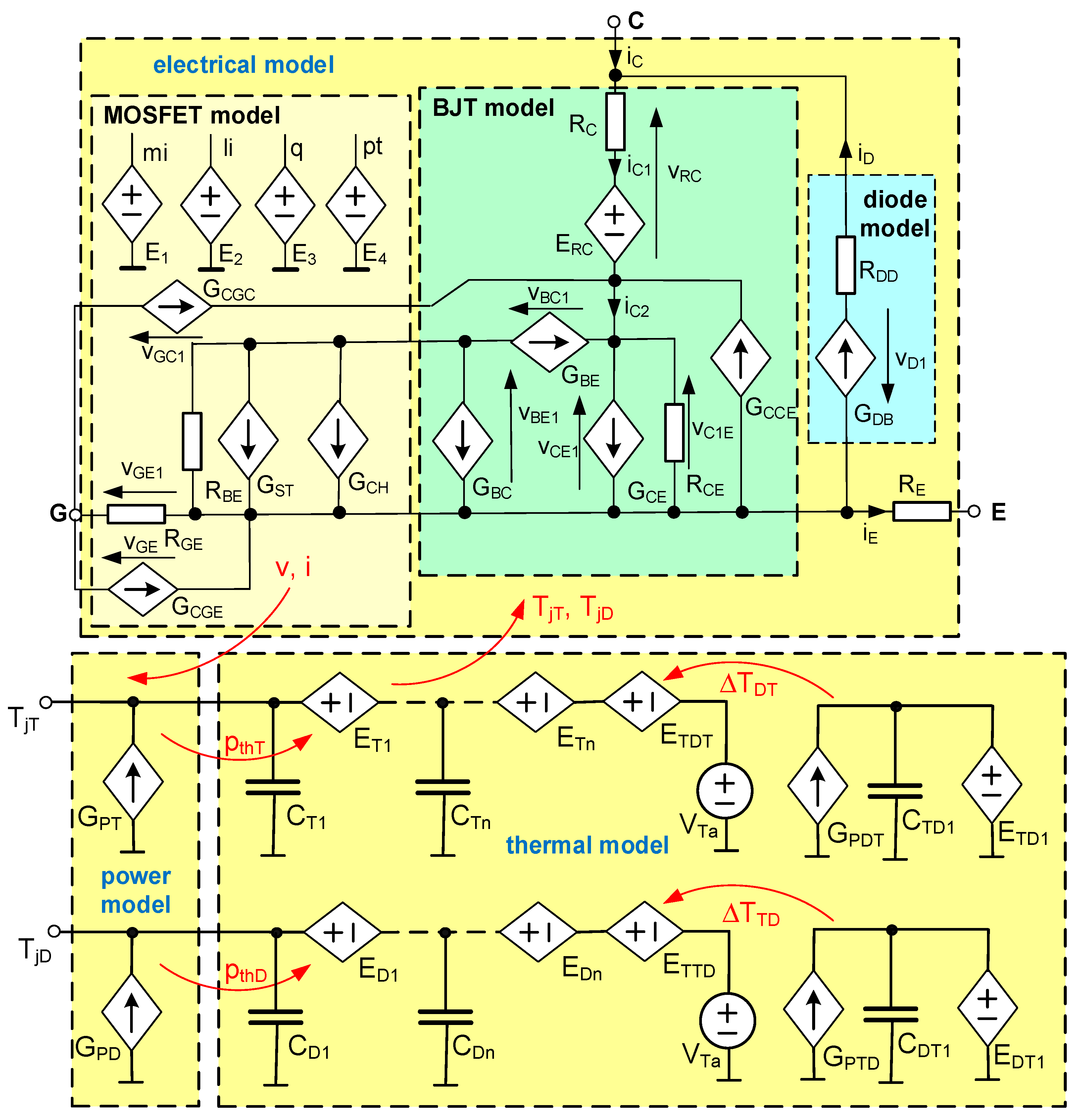
The electrothermal model of the IGBT formulated by the authors has a form of the subcircuit for SPICE. The network representation of this model is presented in Figure 2.
This model consists of three parts: the electrical model, the thermal model, and the power model. In the further part of this section, the mentioned components of the new model are described. Section 2.1 contains a description of the electrical model, the Section 2.2, the power model, whereas Section 2.3, the thermal model.

2.1. Electrical Model

In formulating the electrical model, the classical network representation of the IGBT was used. Therefore, in this model 3 blocks appear. They represent models of the input MOS structure, the output BJT and the diode, respectively. In order to formulate this model, the equations describing the DC characteristics of the transistor MOS given in the paper [50], the equations describing the DC characteristics of the BJT [16] and the equations describing the DC characteristics of the diode proposed in the paper [19] were used. Each dependence existing in the considered model is represented by the controlled voltage and the current sources. These dependences are elaborated for IGBTs made of silicon.
Series resistances of the emitter and the collector are modelled by linear resistors RE and RC. Controlled voltage source ERC models the linear dependence of the collector series resistance RC on temperature. Resistors RCE, RBE and RGE model the leakage currents flowing between each pair of terminals of the transistor.
The drain current of the MOS transistor is modelled by two controlled current sources: GST and GD. The first of these sources model the drain current in the sub-threshold range, whereas the source GD—the channel current of this transistor. The output currents of the mentioned sources are described with the following equations [50]
I G S T = I P O ( T j T T 0 ) exp ( V g o T j T k / q ) ( exp ( L I M I T ( v G E 1 v P H , 0 , v V T v P H ) n P T j T k / q ) 1 )
I G D = B v m i v B E 1 / | v B E 1 |
Values of parameters IPO, np and B occurring in the Equations (1) and (2) correspond to reference temperature T0, Vgo corresponds to a band-gap of silicon and amounts to 1.206 V, TjT is the device internal temperature, k is the Boltzmann constant, and q is the electron charge. LIMIT(x, min, max) is a standard-function of SPICE, whose value is equal to min, if x < min, max, if x > max, and in other cases it is x. Voltages vBE1 and vGE1 are marked in Figure 2. In turn, vmi and vPH mark voltages on terminals of controlled voltage sources E1 and E4, respectively.
Controlled voltage sources E1 and E2 were applied to compute the value of voltage vmi according to the equations contained in the paper [50], and voltages between connectors of controlled voltage sources E3 and E4 describing linear dependences of threshold voltage vVT (E3) and the Fermi level vPH (E4) on temperature.
Current transfluent between the base and the emitter of the bipolar transistor contained in the structure of the modelled IGBT is modelled by controlled current source GBE. The output current of this source is given by the equation:
I G B E = I O β F ( T j T T 0 ) 2 exp ( V g o n 1 T j T k / q ) ( exp ( v B C 1 n 1 T j T k / q ) 1 )
where I0 denotes a model parameter, n1– the emission coefficient of the base-emitter junction, voltage vBC1 is marked in Figure 2, and βF is the coefficient of current amplification of the BJT operating within the forward active mode. The value of this coefficient depends on the collector current iC1 and temperature TjT. This dependence is given in the paper [16].
Controlled current source GBC models current flowing between the base and the collector of the BJT. The current of this source is given by the formula:
I G B C = I O β R ( T j T T 0 ) 2 exp ( V g o n 10 T j T k / q ) ( exp ( v B E 1 n 10 T j T k / q ) 1 )
where n10 is the emission coefficient of the base-collector junction, voltage vBE1 is marked in Figure 2, βR is the coefficient of reverse current amplification of the BJT; βR linearly depends on temperature TjT.
The main current of the IGBT is modelled by controlled current source GCE, whose output current is described by the equation:
I G C E = I O ( T j T T 0 ) 2 exp ( V g o n 1 T j T k / q ) ( 1 + v C E 1 U A N ) ( exp ( v B C 1 n 10 T j T k / q ) exp ( v B E 1 n 1 T j T k / q ) )
where UAN denotes early voltage.
The DC characteristic of the antiparallel diode is modelled by controlled current source GDB. The output current of this source is equal to the sum of diffusive and generation-recombination components and it is described by the formula given in the paper [19].
In order to take into account electric inertia in the described model, three controlled current sources GCGE, GCCE and GCGC are applied. The mentioned sources model current flowing through parasitic capacitances situated between each pair of the transistor removals. Capacitance CGE is connected to the input MOS structure and it is described by the following formula:
C G E = C G E 0 w + x ( T j T T 0 ) + { 0   i f   v G E < V G E min + v C 1 E C o x k 1 ( C G 1 V G C 1 + C G 2 )   i f   V G E min + v C 1 E < v G E V G E max + v C 1 E   C o x   i f   v G E > V G E max + v C 1 E   a n d   v C 1 E < 0   C o x [ u ( T j T T 0 ) + 0.75 ( v G C 1 2 v G E + v C 1 E ) 2 ]   i f   v G E > V G E max + v C 1 E   a n d   v C 1 E 0
where Cox means capacitance dependent on thickness tOX of the layer of SiO2 under the gate, w is width of the channel of the MOS structure, CGE0 is capacitance between the gate and the emitter per unit of widths of the channel, VGEmax, VGEmin, CG1, CG2, x, u and k1 are parameters of the model, whereas voltages vGE, vGC1 and vC1E are marked in Figure 2.
Capacitance Cox occurring in the Equation (6) is connected with the SiO2 layer under the gate of the transistor and it is described by the formula [47]
C o x = ε 0 ε o x L w t O X
where L denotes the length of the channel of the MOS structure, ε0 is dielectric permeability of free air, and εox—relative dielectric permeability of silicon.
In turn, the output capacitance of the modelled device corresponds to the junction capacitance of the antiparallel diode and it is described by the following equation:
C C E = C C E 0 ( 1 + v C E / V j ) M j ( 1 + r ( T j D T 0 ) )
where vCE denotes the collector-emitter voltage, CCE0 is output capacitance at zero voltage on the antiparallel diode, Vj is built-in potential of this diode, Mj is a parameter describing the doping profile of the junction of this diode, r is the temperature coefficient of parameter Mj.
Capacitance between the gate and the collector corresponds to capacitance of the base-emitter junction of the BJT and to the gate-drain capacitance of the MOS transistor and it is described by the dependence of the form
C G C = C 2 i C q k T j T + { C 1 w   i f   v G C 1 < V G C min + e ( T j T T 0 ) [ C G D O + y ( T j T T 0 ) ] w ( 1 + v C 1 E V j C ) M j 2 + n ( T j T T 0 ) i f   v G C 1 V G C min + e ( T j T T 0 )
where CGD0 is capacitance between the gate and the drain per unit of widths of the channel, C1, C2, y, e, n, VGCmin are parameters of the model, VjC is built-in potential of the base-emitter junction of the BJT, Mj2 is a parameter describing the doping profile of this junction.
The output currents of the considered controlled current sources (GCCE, GCGE and GCGC) are equal to the product of capacitances described by the Equations (6)–(9) and the time derivative of the voltage on these sources. The network used to compute each capacitive current contains the controlled current source GC1 modelling parasitic capacitance, the linear capacitor of the fixed capacitance connected in series to the voltage sources of zero value.

2.2. Power Model

The power model describes the dependence of thermal power dissipated in the transistor and in the diode on terminal voltages and currents of the modelled device. Thermal power is equal to the difference between the total power lost in this transistor and the instantaneous power dissipated in internal capacitances of this device [50].
For the modelled transistor, power pthT is described by the Formula (10), whereas power pthD dissipated in the diode is given by the Formula (11).
p t h T = i C 1 v R C + i C 2 v C 1 E + R E i E 2
p t h D = i D 2 R D D + i D v D 1
where currents iD, iC1, iC2 and iE, as well as voltages vRC and vCE1 are marked in Figure 2.
In Figure 2 thermal power pthT is represented by controlled current source GPT, the current of which is given by the Equation (10), whereas thermal power pthD, by controlled current source GPD given by the Equation (11).

2.3. Thermal Model

The thermal model describes the dependence of internal temperatures TjT of the transistor and TjD of the diode on thermal power dissipated in these components pthT and pthD, respectively. This model describes self-heating in the transistor and in the diode as well as mutual thermal couplings between them. This model is described by the network analogue containing four non-linear Cauer networks proposed in the paper [49]. This model takes into account the influence of ambient temperature Ta and the transistor and the diode internal temperatures TjT and TjD on thermal resistances occurring in this model. For example, thermal resistance of transistor RthT is described by means of the equation of the form
R t h T = R t h T 1 ( 1 a ( T a T 0 ) ) exp ( ( T j T T a ) / T z ) + R t h T 0 ( 1 b ( T a T 0 ) )
where RthT1, RthT0, a, b, T0 and TZ are model parameters.
In the network representation of the thermal model of the modelled device, four subcircuits occur. The networks visible on the right-hand side model mutual thermal coupling between the diode and the transistor, whereas the networks visible on the left-hand side model self-heating in the transistor and in the diode. Voltage source VTa represents ambient temperature Ta, capacitors correspond to heat capacitances of each component of the heat flow path, whereas controlled voltage sources ET1, …, ETn describe dependences RthT(Ta, TjT), ED1, …, EDn describes dependences RthD(Ta, TjD), and EDT1 and ETD1, dependences of transfer thermal resistances RthDT(Ta, TjD) and RthTD(Ta, TjT), respectively. Controlled voltage sources ETTD and ETDT model an increase of internal temperatures of the transistor and the diode, respectively, caused by mutual thermal couplings between these devices.

3. Estimation of the Model Parameters

The practical application of the formulated model demands an effective procedure to estimate values of its parameters. Such a procedure was prepared based on the idea of the local estimation described in the paper [51].
According to this idea, the value of each parameter of the model is estimated on the basis of the coordinates of points lying on the measured characteristics of the investigated device. These points are selected in such a manner that the considered characteristics can be described with the use of the simplified analytic formulas, containing fewer parameters. After transforming these formulas, the equations make it possible to calculate values of each parameter of the formulated model.
Values of parameters are computed in the strictly defined order in a multi-stage procedure including measurements and computations. Practical equations used to compute the value of each parameter contain the coordinates of measuring points and values of parameters of the model estimated in the previous stages of the estimation procedure.
The procedure of estimating the values of parameters of the electrical model of the IGBT is described in the paper [19], whereas the manner of estimating parameters of the thermal model is presented in the paper [49]. While estimating values of parameters of the electrical model, suitable current-voltage characteristics or dependences of capacitances on voltages measured at selected values of ambient temperature and in the conditions making it possible to omit self-heating phenomena are used. In turn, to compute the value of parameters of the thermal model, waveforms of transient thermal impedance measured at selected values of ambient temperature and power dissipated in the modelled transistor are used.

4. Verification of the Formulated Model

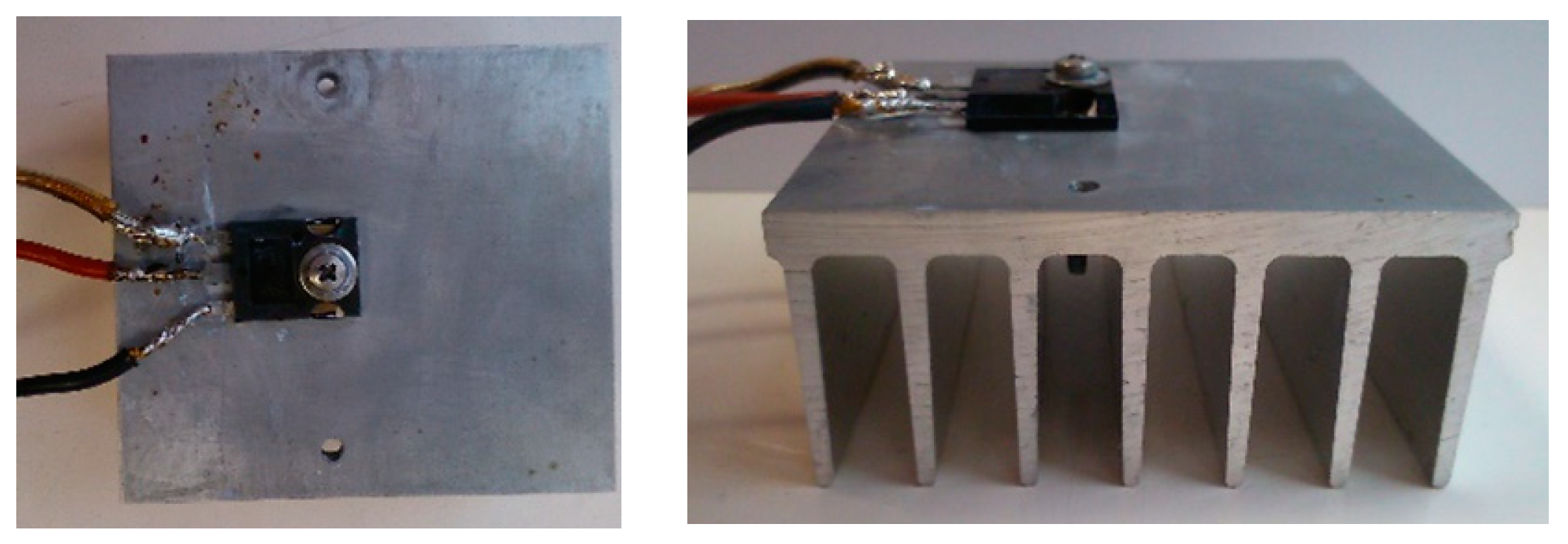
In order to verify the correctness of the proposed model, the DC and dynamic characteristics of the silicon IGBT of the type IRG4PC40UD [52] operating in different cooling conditions were measured and computed with the use of this model. This transistor is characterised by the maximum allowable value of collector current equal to 15 A and the maximum allowable value of collector-emitter voltage equal to 600 V [52]. The estimated value of the threshold voltage of the investigated transistor is equal to Vth0 = 5.82 V at temperature T0 = 300 K. Investigations were performed for the mentioned device contained in the case TO-247 situated on the heat-sink shown in Figure 3 and for this device operating without any heat-sink. The results of these measurements and computations are presented in Figure 4, Figure 5, Figure 6, Figure 7, Figure 8 and Figure 9 in this Section.
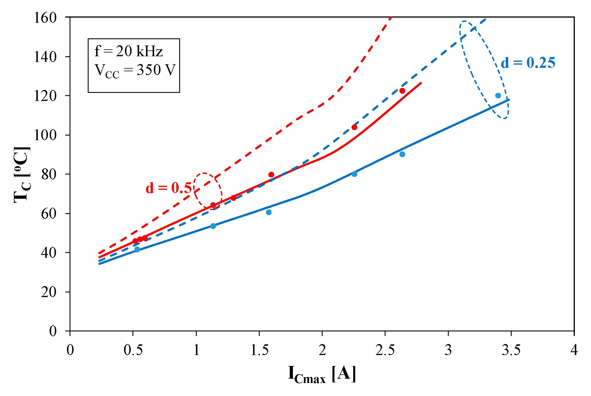
In all these figure’s points represent the results of measurements, and solid lines—the results of computations obtained by means of the formulated model (ETN). Dashed lines represent the results of computations obtained with the use of the same electrothermal model containing the linear thermal model (ETL), in which the dependence Rth(Tj, Ta) is omitted. At first, the DC characteristics of the considered transistor are presented, and next, the results of investigations on its dynamic proprieties are shown. Additionally, the results of computations obtained with the use of the model performed by A.R. Hefner and described in the papers [18,53,54,55] are marked with dotted lines (ETH). The isothermal version of this model is built-in in the current version of the SPICE software commonly used in analyses of electronic and power electronic networks. In the computations performed with this model, self-heating phenomena are taken into account using the separated iterations method described in [56]. The values of the model parameters were estimated using the PSPICE Model Editor, which is a part of the SPICE software. The PSPICE Model Editor uses the catalogue data as the input data. The case temperature TC is measured with the use of an infrared pyrometer. The values of this temperature are computed with the use of the following formula [23].
T C = T a + T j T T a R t h T ( R t h T R t h j C )
where Rthj-c denotes thermal resistance between the die of the IGBT and the device case. The value of this parameter is given by the producer [52].
In order to obtain the characteristics presented in the further part of this section, we performed the classical DC sweep or transient analyses in the PSPICE software using the considered models of the IGBT. The computations were performed in classical networks used to measure the considered characteristics including voltage sources, resistors and the tested IGBT. In each characteristic, the results corresponding to the thermally steady state are presented.
In Figure 4, the output characteristics of the tested transistor (Figure 4a) obtained at strong steering (voltage VGE = 10 V) and, corresponding to them, dependences of the case temperature TC of the transistor on its output voltage (Figure 4b) are presented. The results obtained for the transistor situated on the heat-sink are marked with blue colour, and for the transistor operating without any heat-sink, with red colour.
As can be observed in Figure 4a, all the presented characteristics are monotonically increasing functions. The slope of these functions visibly increases for voltage VCE > 0.9 V. The cooling conditions of the transistor do not influence in an essential manner the obtained courses of characteristics IC(VCE). With the worsening cooling conditions, a small shift left of the considered characteristics is visible. It is connected with a decrease of the forward voltage of the base-emitter junction of the internal BJT due to an increase in internal temperature TjT. For the models ETN and ETL, a good agreement between the results of computations and measurements is obtained (the differences are smaller than 0.1 A), whereas the results obtained by the Hefner model visibly differ from the results of measurements (the differences exceed even 90%).
Cooling conditions strongly influence the dependence TC(VCE) shown in Figure 4b. This dependence is an increasing function. At the collector current equal to about 3 A (at VCE = 1.2 V), the transistor without any heat-sink attains the case temperature equal even to 100 °C. Meanwhile, for the transistor operating on the heat-sink at current IC = 10 A (at VCE = 1.7 V) temperature TC reaches only just 80 °C. The differences between the results of measurements and computations performed with the ETN do not exceed a few celsius degrees. For the other considered models, these differences are much more visible, even exceeding 50 °C.
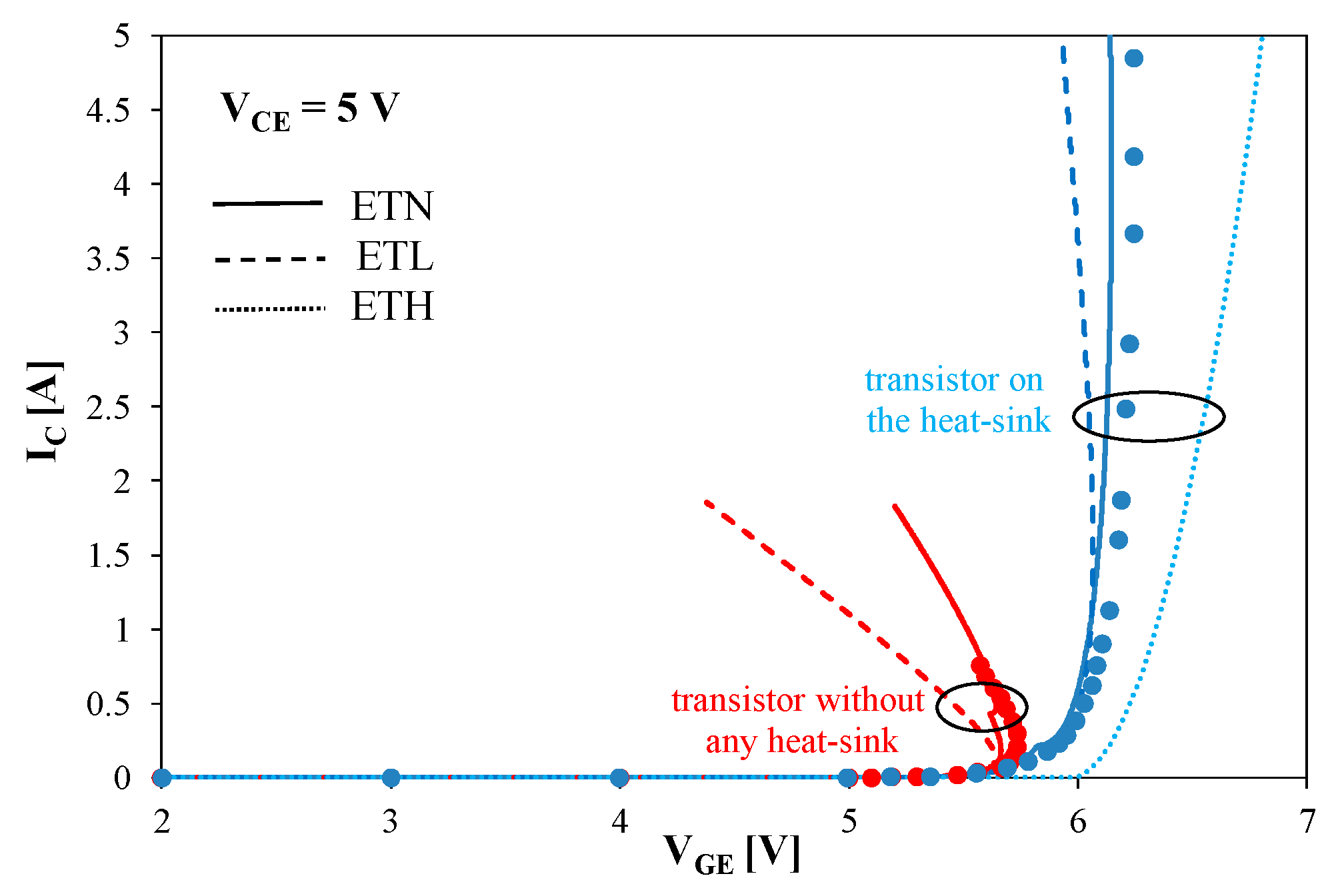
Figure 5 illustrates transfer characteristics of the tested transistor.
The characteristics IC(VGE) obtained at different cooling conditions of the transistor differ in shape. For the transistor situated on the heat-sink, the measured dependence IC(VGE) is an increasing function. In turn, the characteristic for the transistor without any heat-sink shows a negative slope at current IC > 0.2 A. This non-typical shape of the considered characteristic results from a rise of internal temperature of the transistor and a fall in the value of its threshold voltage. At current IC = 1 A voltage, VGE decreases even by 0.5 V as a result of changes of the cooling conditions, causing an increase in the case temperature TC even by 85 °C. The characteristics obtained with the Hefner model are practically the same for both types of the cooling conditions and they do not change with temperature TC due to neglecting the sub-threshold effect in this model. For the ENL model, the value of temperature TC is overestimated and the characteristics IC(VGE) show a shift to the left and differ visibly from the measurement results. The differences in the measured and computed with the ETN model values of VGE voltage do not exceed 0.1 V, whereas for the other models these differences exceed even 1 V and they increase with an increase of IC current.
At weak steering (at values VGE nearing the value of the threshold voltage) ambiguous output characteristics of the considered transistor are obtained. These characteristics are shown in Figure 6a for the transistor operating without any heat-sink and in Figure 6b for the transistor situated on the heat-sink, whereas the corresponding dependences of the case temperature on voltage VCE are shown in Figure 7.
At both types of the cooling conditions ambiguous characteristics IC(VCE) are obtained. On each characteristic, the point of the electrothermal breakdown, in which the sign of the slope of these characteristics changes from the positive to negative, is visible. Such a shape of the output characteristics is well-known for other power semiconductor devices, e.g., power MOS transistors [50] and power BJTs [16]. Such a shape of the output characteristics also means that the breakdown in the investigated transistor can be observed at a considerably lower value of voltage VCE than its admissible catalogue value.
As it is visible in Figure 6, the breakdown can appear even for VCE smaller than 10 V, whereas the admissible value of this voltage given by the producer amounts to 600 V [52]. It is worth noticing that the value of voltage VCE, at which the electrothermal breakdown appears, decreases together with an increase in voltage VGE and when its cooling conditions worsen.
While analysing characteristics TC(VCE) it is visible that in the point of the electrothermal breakdown temperature, TC amounts to about 50 °C. This means that an increase in internal temperature of the investigated device over ambient temperature equal to about 30 °C is sufficient for the electrothermal breakdown to occur. The value of this increase is practically the same for both the considered types of cooling conditions.
In Figure 6, the results obtained with the use of the Hefner model overlap with the VCE axis due to the omission of the sub-threshold effect in this model. As a result of a very low value of current iC obtained using this model, values of the computed temperature TC (shown in Figure 7) are practically equal to the ambient temperature. For the ETL model, the computed value of the voltage corresponding to electrothermal breakdown is underestimated even by 3 V due to the overestimation of TjT temperature. It is a result of omitting in this model the dependence of the thermal resistance on the device internal temperature.
The next figures (Figure 8 and Figure 9) illustrate the influence of self-heating phenomena on parameters values of a switching process of the transistor. This transistor is excited by a rectangular pulses train of frequency f, duty cycle d and voltage levels equal to zero and 15 V, respectively. The circuit of the collector is supplied from voltage source VCC through resistor RL.
In order to take into account self-heating phenomena in transient analyses of the circuits described by means of considerably different time constants, a special method of the analysis described in the paper [57] is applied. In this method only one non-physical thermal time constant of the value considerably longer than electrical time constants characterising the examined circuit is used. In the case of the considered model of the IGBT in its thermal model, only one capacitor representing heat capacitance of the arbitrarily selected value 50 μJ/K and one controlled voltage source representing thermal resistance of the whole transistor are used.
In the paper [28], we showed that in the isothermal conditions the computed by means of the considered electrical model and measured waveforms of the collector current of the IGBT at switching were convergent. A good agreement between the results of computations and measurements was obtained in wide ranges of the values of load resistance and voltage supplying the collector circuit changed. In the cited paper, it is also shown that the waveforms iC(t) computed using the Hefner model visibly differ from the results of measurements. The values of switch-on and switch-off times obtained with this model differ even by 50% from the results of measurements. Therefore, in order to have the clear picture of the presented results of the investigations, the results obtained using the Hefner model are omitted in Figure 8 and Figure 9.
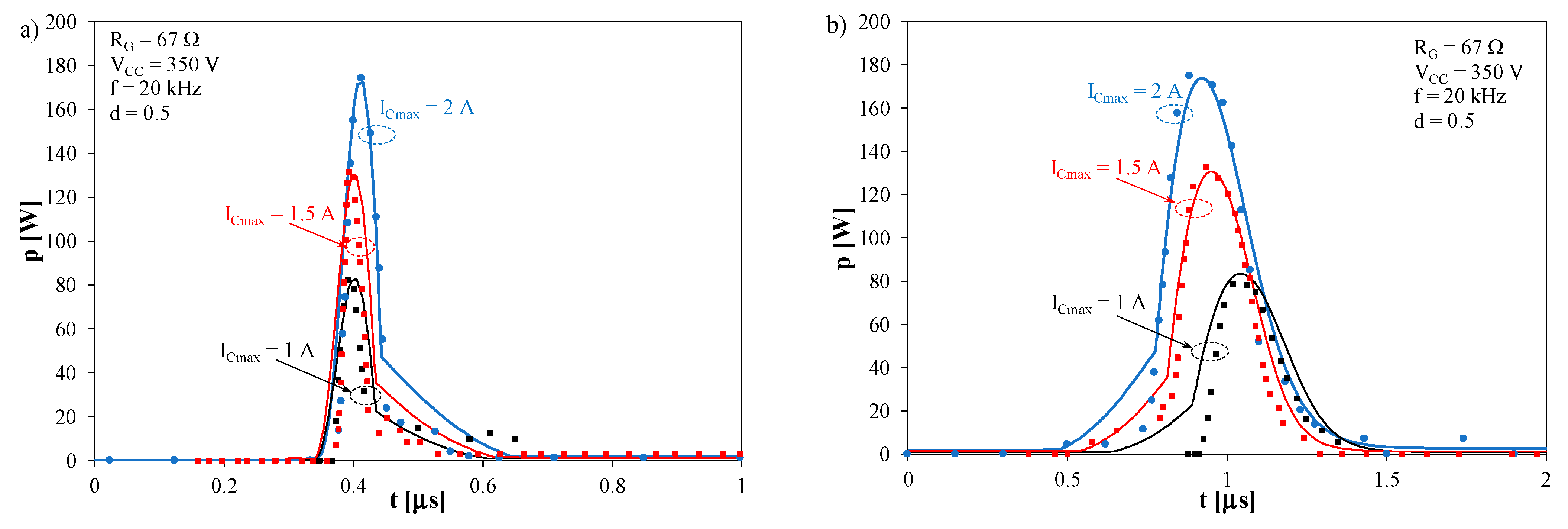
In Figure 8 and Figure 9, the results of computations and measurements at the thermally steady state are presented. In Figure 8, waveforms of power lost in the transistor when switched-on (Figure 8a) and switched-off (Figure 8b) at selected values of current of the switched-on transistor ICmax are shown.
It is proper to notice that power losses at switching-on and switching-off are considerably bigger than power losses at the on and off states of the transistor. In the impulse this power attains even 180 W. The time duration of a switching process causes energy at switching-off to. be higher than energy at switching-on. The values of these energies are computed as a result of integration of the shown waveforms p(t). Together with an increase in the value of current ICmax, the maximum value of power lost in the transistor in the switching process increases. A very good agreement between the results of measurements and computations is obtained.
In Figure 9, the computed and measured dependences of the case temperature of the transistor without any heat-sink operating in the considered switch with resistive load on current ICmax are shown. The presented results were obtained at frequency of the control signal f = 20 kHz and selected values of the duty cycle d.
It is visible that for both values of the duty cycle, the dependence TC(ICmax) is an increasing function. An increase in the value of the coefficient d causes also an increase in temperature TC. At lower values of the coefficient d, the operation of the transistor with a higher value of the collector current at the on-state is possible without a risk of exceeding the admissible value of internal temperature. For the ETN model, a very good agreement between the results of computations and measurements is obtained. The differences do not exceed 2 °C, whereas for the ETL model these differences are much bigger, even up to 40 °C.

5. Conclusions

In this paper a new compact large-signal electrothermal model of the IGBT dedicated for SPICE was proposed. This model makes it possible to compute the values of terminal voltages and currents of the considered device and its internal temperature taking into account both electrical phenomena occurring in this device and self-heating phenomena. The formulated model takes into account such phenomena that are omitted in other models of this device described in the literature: operation in the sub-threshold region and the nonlinearity of thermal properties of the modelled device, which means the dependence of thermal resistance on internal temperature and ambient temperature.
The correctness of the model was verified experimentally at both the dc and dynamic operating conditions of the investigated transistor. Different cooling conditions of this transistor were taken into account. It was proved that for all the considered cases of the operation of the investigated device, a good agreement between the results of computations and measurements was obtained using our model (ETN). It was also shown that at weak control of the investigated device, the accuracy obtained using our model was much better than for the classical models presented in the literature. The characteristics obtained for this range using the ETH have different shapes than the measured characteristics. In turn, the use of the ETL causes underestimating of VCE voltage in the electrothermal breakdown range even by 3 V. In contrast, for the ETN these differences are much smaller and they do not exceed 0.2 V. The ETN model makes it also possible to compute more accurately the device internal and case temperatures than the other considered models.
The presented results of computations and measurements illustrate interesting properties of the considered device. Among other things, it was shown that the ambiguous non-isothermal characteristics IC(VGE) of the transistor can be obtained. It was also shown that at the values of voltage VGE nearing the threshold voltage, the ambiguous non-isothermal output characteristics of this transistor can be obtained. At these characteristics the so-called electrothermal breakdown is observed. This breakdown appears at the values of the transistor output voltage VCE considerably lower than the admissible catalogue value of this voltage. The electrothermal breakdown can be a destructive occurrence for the investigated device. It was also observed that an increase in the internal temperature of the transistor only just by 30 °C above ambient temperature was sufficient to cause the electrothermal breakdown. It was proved that a good agreement between the computed and measured characteristics of the IGBT operating at different cooling conditions in a wide range of changes of its terminal currents and voltages is possible to achieve only taking into account the nonlinearity of the thermal model.
When the transistor operates as a switch with resistive load, one can notice that on-time and off-time of the transistor change with the changes in the value of the collector current in the on-state. Additionally, the value of internal temperature of the transistor at the steady-state strongly depends on load resistance, frequency and the duty cycle of the signal controlling the gate of such a transistor. It is a result of dynamic power losses in the IGBT, which are properly described in the proposed model.
The proposed model of the IGBT was elaborated and verified for the devices made of silicon only. This model can be useful for designers of electronic and power electronic networks containing the IGBT. The presented characteristics of this transistor will help also identify the causes of damage of the networks containing IGBTs.

Author Contributions

Conceptualization, P.G. and K.G.; methodology, P.G., K.G. and J.Z.; investigation, P.G. and K.G.; writing—original draft preparation, P.G. and K.G.; writing—review and editing, K.G., P.G. and J.Z.; visualization P.G. and K.G.; supervision, K.G. and J.Z.; funding acquisition, P.G. All authors have read and agreed to the published version of the manuscript.

Funding

The scientific work financed with the Polish science budget resources in the years 2017–2021, as the investigation project No. DI 2015 0075 45 within the framework of the program “Diamentowy Grant”.

Institutional Review Board Statement

Not applicable.

Informed Consent Statement

Not applicable.

Data Availability Statement

Data is contained within the article.

Conflicts of Interest

The author declares no conflict of interest.

Nomenclature

isothermal characteristicscharacteristics determined at a constant value of the device internal temperature
non-isothermal characteristicscharacteristics determined with thermal phenomena taken into account
electrothermal modela model describing current-voltage-temperature dependences with thermal phenomena taken into account
iCcollector current of the IGBT
kthe Boltzmann constant
LIMIT(x, min, max)a standard-function of SPICE, whose value is equal to min, if x < min, max, if x > max, and in other cases it is equal to x
pthTthermal power dissipated in the transistor
pthDthermal power dissipated in the diode
qelectron charge
RthTthermal resistance of the transistor
RthDthermal resistance of the diode
RthTDtransfer thermal resistance between the transistor and the diode
RthT1, RthT0, a, b, TZparameters occurring in the dependence RthT(Ta, TjT)
Taambient temperature
TjDinternal temperature of the diode
TjTinternal temperature of the IGBT
T0reference temperature
vBE1, vGE1, vBC1, vGE, vGC1, vC1Evoltages between the internal terminals of the BJT and the MOSFET contained in the structure of the IGBT marked in Figure 2
vCEcollector-emitter voltage of the IGBT
vGEgate-emitter voltage of the IGBT
Vgovoltage corresponding to a band-gap of silicon
ε0dielectric permeability of free air
εoxrelative dielectric permeability of silicon
Parameters of a MOS transistor:
Bparameter of the main component of drain current
CGD0capacitance between the gate and the drain per unit of widths of the channel
CGE0capacitance between the gate and the emitter per unit of widths of the channel
Coxcapacitance dependent on thickness tOX of the layer of SiO2 under the gate
C1, C2, y, e, n, VGCminparameters describing CGD0 capacitance
iD, iC1, iC2, iEcurrents marked in Figure 2
IPOparameter of sub-threshold current
Llength of the channel
npthe emission coefficient of sub-threshold current
vmivoltages on terminals of controlled voltage sources E1, to which the main part of drain current is proportional; the value of this voltage depends on voltages vGE1, vBG1 and vVT
vPHthe Fermi level linearly dependent on temperature TjT
vVTthreshold voltage linearly dependent on temperature TjT
wwidth of the channel
VGEmax, VGEmin, CG1, CG2, x, u and k1parameters of the model describing CGE0 capacitance
Parameters of a BJT:
I0parameter, to which the collector current is proportional
Mj2parameter describing the doping profile of the base-emitter junction
n1the emission coefficient of the base-emitter junction
UANEarly voltage
VjCbuilt-in potential of the base-emitter junction
vRC, vCE1voltages between the internal terminals of the BJT marked in Figure 2
βFthe current amplification coefficient within the forward active mode; this coefficient depends on temperature TjT and the collector current
Parameters of a diode:
CCE0capacitance at zero voltage on the diode
I0Dparameter, to which the diode current is proportional
Mjparameter describing the doping profile of the junction
nDthe emission coefficient of the diode
rthe temperature coefficient of parameter Mj.
Vjbuilt-in potential

References

  1. Baliga, B.; Adler, M.; Love, R.; Gray, P.; Zommer, N. The insulated gate transistor: A new three-terminal MOS-controlled bipolar power device. IEEE Trans. Electron. Devices 1984, 31, 821–828. [Google Scholar] [CrossRef]
  2. Iwamuro, N.; Laska, T. IGBT History, state-of-the-art, and future prospects. IEEE Trans. Electron. Devices 2017, 64, 741–752. [Google Scholar] [CrossRef]
  3. Choi, U.-M.; Vernica, I.; Blaabjerg, F. Effect of asymmetric layout of IGBT Modules on reliability of motor drive inverters. IEEE Trans. Power Electron. 2019, 34, 1765–1772. [Google Scholar] [CrossRef] [Green Version]
  4. Yaghoubi, M.; Moghani, J.S.; Noroozi, N.; Zolghadri, M.R. IGBT open-circuit fault diagnosis in a quasi-z-source inverter. IEEE Trans. Ind. Electron. 2019, 66, 2847–2856. [Google Scholar] [CrossRef]
  5. Bae, C.; Lee, D.; Nguyen, T.H. Detection and identification of multiple IGBT open-circuit faults in PWM inverters for AC machine drives. IET Power Electron. 2019, 12, 923–931. [Google Scholar] [CrossRef]
  6. Li, B.; Zhao, X.; Cheng, D.; Zhang, S.; Xu, D.G. Novel hybrid DC/DC converter topology for HVDC interconnections. IEEE Trans. Power Electron. 2019, 34, 5131–5146. [Google Scholar] [CrossRef]
  7. Wang, J.; Li, Z.; Jiang, X.; Zeng, C.; Shen, Z.J. Gate control optimization of Si/SiC hybrid switch for junction temperature balance and power loss reduction. IEEE Trans. Power Electron. 2019, 34, 1744–1754. [Google Scholar] [CrossRef]
  8. Dudrik, J.; Pastor, M.; Lacko, M.; Zatkovic, R. Zero-voltage and zero-current switching PWM DC–DC converter using controlled secondary rectifier with one active switch and nondissipative turn-off snubber. IEEE Trans. Power Electron. 2017, 33, 6012–6023. [Google Scholar] [CrossRef]
  9. Górecki, K.; Detka, K. Application of average electrothermal models in the spice-aided analysis of boost converters. IEEE Trans. Ind. Electron. 2019, 66, 2746–2755. [Google Scholar] [CrossRef]
  10. Hefner, A.R.; Diebolt, D.M. An experimentally verified igbt model implemented in the saber circuit simulator. In Proceedings of the PESC ‘91 Record. 22nd Annual IEEE Power Electronics Specialists Conference, Cambridge, MA, USA, 24–27 June 1991; IEEE: Piscataway Township, NJ, USA, 2002; Volume 9, pp. 532–542. [Google Scholar] [CrossRef]
  11. Riccio, M.; De Falco, G.; Mirone, P.; Maresca, L.; Tedesco, M.; Breglio, G.; Irace, A. Accurate SPICE modeling of reverse-conducting IGBTs including self-heating effects. IEEE Trans. Power Electron. 2017, 32, 3088–3098. [Google Scholar] [CrossRef]
  12. Azar, R.; Udrea, F.; Ng, W.T.; Dawson, F.; Findlay, W.; Waind, P.; Amaratunga, G. Advanced electrothermal SPICE modelling of large power IGBTs. IEE Proc. Circuits Devices Syst. 2004, 151, 249–253. [Google Scholar] [CrossRef] [Green Version]
  13. Bagnoli, P.E.; Casarosa, C.; Ciampi, M.; Dallago, E. Thermal resistance analysis by induced transient (TRAIT) method for power electronic devices thermal characterization—part I: Fundamentals and theory. IEEE Trans. Power Electron. 1998, 13, 1208–1219. [Google Scholar] [CrossRef]
  14. Deng, E.; Zhao, Z.; Zhang, P.; Li, J.; Huang, Y. Study on the methods to measure the junction-to-case thermal resistance of IGBT modules and press pack IGBTs. Microelectron. Reliab. 2017, 79, 248–256. [Google Scholar] [CrossRef]
  15. Bryant, A.T.; Mawby, P.A.; Palmer, P.R.; Santi, E.; Hudgins, J.L. Exploration of Power Device Reliability Using Compact Device Models and Fast Electrothermal Simulation. IEEE Trans. Ind. Appl. 2008, 44, 894–903. [Google Scholar] [CrossRef]
  16. Zarębski, J.; Górecki, K. SPICE-aided modelling of dc characteristics of power bipolar transistors with self-heating taken into account. Int. J. Numer. Model. Electron. Netw. Devices Fields 2009, 22, 422–433. [Google Scholar] [CrossRef]
  17. Górecki, K.; Górecki, P. Modelling the influence of self-heating on characteristics of IGBTs. In Proceedings of the 21st International Conference Mixed Design of Integrated Circuits and Systems (MIXDES), Lublin, Poland, 19–21 June 2014; IEEE: Piscataway Township, NJ, USA, 2014; pp. 298–302. [Google Scholar]
  18. Hefner, A.R. Dynamic electro-thermal model for the IGBT. IEEE Trans. Ind. Appl. 1994, 30, 394–405. [Google Scholar] [CrossRef]
  19. Górecki, P.; Górecki, K.; Zarębski, J. Modelling the temperature influence on dc characteristics of the IGBT. Microelc. Reliab. 2017, 79, 96–103. [Google Scholar] [CrossRef]
  20. Rashid, M. SPICE for Power Electronics and Electronic Power, 3rd ed.; Taylor and Francis Group: Oxfordshire, UK, 2016. [Google Scholar]
  21. Eguchi, K.; Asadi, F.; Kuwahara, K.; Ishibashi, T.; Oota, I. A small direct SC AC-AC converter with cascade topology. Int. J. Innov. Comput. Inf. Control 2018, 14, 1741–1753. [Google Scholar]
  22. Detka, K.; Górecki, K.; Zarębski, J. Modeling single inductor DC–DC converters with thermal phenomena in the inductor taken into account. IEEE Trans. Power Electron. 2017, 32, 7025–7033. [Google Scholar] [CrossRef]
  23. Górecki, P.; Wojciechowski, D. Accurate computation of IGBT junction temperature in PLECS. IEEE Trans. Electron. Devices 2020, 67, 2865–2871. [Google Scholar] [CrossRef]
  24. Basso, C. Switch-Mode Power Supply SPICE Cookbook; McGraw-Hill: New York, NY, USA, 2001. [Google Scholar]
  25. Maksimovic, D.; Stankovic, A.M.; Thottuvelil, V.J.; Verghese, G.C. Modeling and simulation of power electronic converters. Proc. IEEE 2001, 89, 898–912. [Google Scholar] [CrossRef]
  26. Napieralski, A.; Napieralska, M. Polowe Półprzewodnikowe Przyrządy Dużej Mocy; Wydawnictwo Naukowo-Techniczne: Warszawa, Poland, 1995. (In Polish) [Google Scholar]
  27. Rashid, M.H.; Rashid, H.M. Spice for Power Electronics and Electric Power; CRC Press: Boca Raton, FL, USA, 2006. [Google Scholar]
  28. Górecki, P.; Górecki, K. Modelling a switching process of IGBTs with influence of temperature taken into account. Energies 2019, 12, 1894. [Google Scholar] [CrossRef] [Green Version]
  29. Wilamowski, B.; Jager, R.C. Computerized Circuit Analysis Using SPICE Programs; McGraw-Hill: New York, NY, USA, 1997. [Google Scholar]
  30. Sheng, K.B.; Williams, W.; Finney, S.J. A review of IGBT models. IEEE Trans. Power Electron. 2000, 15, 1250–1266. [Google Scholar] [CrossRef]
  31. Gamage, S.; Pathirana, V.; Udrea, F. Electrothermal model for an SOI-based LIGBT. IEEE Trans. Electron. Devices 2006, 53, 1698–1704. [Google Scholar] [CrossRef]
  32. Ji, S.Q.; Zhao, Z.M.; Lu, T.; Yuan, L.Q.; Yu, H.L. HVIGBT physical model analysis during transient. IEEE Trans. Power Electron. 2013, 28, 2616–2624. [Google Scholar] [CrossRef]
  33. Xu, Y.; Ho, C.N.M.; Ghosh, A.; Muthumuni, D. A behavioral transient model of IGBT for switching cell power loss estimation in electromagnetic transient simulation. In Proceedings of the 2018 IEEE Applied Power Electronics Conference and Exposition (APEC), San Antonio, TX, USA, 4–8 March 2018; IEEE: Piscataway Township, NJ, USA, 2018; pp. 270–275. [Google Scholar]
  34. Xue, P.; Fu, G.; Zhang, N. Modeling inductive switching characteristics of high-speed buffer layer IGBT. IEEE Trans. Power Electron. 2016, 32, 3075–3087. [Google Scholar] [CrossRef]
  35. Musikka, T.; Smirnova, L.; Niemelä, M.; Silventoinen, P.; Pyrhönen, O. Modelling of high-power IGBT module short-circuit operation and current distribution by a behavioural model. IET Power Electron. 2016, 9, 2700–2705. [Google Scholar] [CrossRef]
  36. Yang, X.; Otsuki, M.; Palmer, P.R. Physics-based insulated-gate bipolar transistor model with input capacitance correction. IET Power Electron. 2015, 8, 417–427. [Google Scholar] [CrossRef]
  37. Duan, Y.; Xiao, F.; Luo, Y.; Iannuzzo, F. A lumped-charge approach based physical SPICE-model for high power soft-punch through IGBT. IEEE J. Emerg. Sel. Top. Power Electron. 2019, 7, 62–70. [Google Scholar] [CrossRef] [Green Version]
  38. Wang, Z.; Qiao, W.; Tian, B.; Qu, L. An effective heat propagation path-based online adaptive thermal model for IGBT modules. In Proceedings of the 2014 IEEE Applied Power Electronics Conference and Exposition—APEC, Fort Worth, TX, USA, 16–20 March 2014; IEEE: Piscataway Township, NJ, USA, 2014; pp. 513–518. [Google Scholar]
  39. Marcault, E.J.; Massol, L.; Tounsi, P.; Dorkel, J.M. Distributed electrothermal modelling methodology for MOS gated power devices simulations. In Proceedings of the MIXDES 2013: 20th International Conference Mixed Design of Integrated Circuits and Systems, Gdynia, Poland, 20–22 June 2013; pp. 301–305. [Google Scholar]
  40. Sfakianakis, G.E.; Nawaz, M. Development of a modeling platform for 4.5 kV IGBT power modules. Proceedings of IECON 2014—40th Annual Conference of the IEEE Industrial Electronics Society, Dallas, TX, USA, 29 October–1 November 2014; IEEE: Piscataway Township, NJ, USA, 2014; pp. 1416–1422. [Google Scholar]
  41. Wu, R.; Wang, H.; Pedersen, K.B.; Ma, K.; Ghimire, P.; Iannuzzo, F.; Blaabjerg, F. A temperature-dependent thermal model of IGBT modules suitable for circuit-level simulations. IEEE Trans. Ind. Appl. 2016, 52, 3306–3314. [Google Scholar] [CrossRef] [Green Version]
  42. Hyeong-Seok, O.; El Nokali, M. A new IGBT behavioral model. Solid State Electron. 2001, 45, 2069–2075. [Google Scholar]
  43. Iannuzzo, F.; Busatto, G. Physical CAD model for high-voltage IGBTs based on lumped-charge approach. IEEE Trans. Power Electron. 2004, 19, 885–893. [Google Scholar] [CrossRef]
  44. Meng, J.; Ning, P.; Wen, X. A physical modeling method for NPT IGBTs verified by experiments. In Proceedings of the IEEE Conference and Expo Transportation Electrification, Asia-Pacific (ITEC Asia-Pacific), Beijing, China, 31 August–3 September 2014; IEEE: Piscataway, NJ, USA, 2014; pp. 1–6. [Google Scholar]
  45. Górecki, P.; Górecki, K. Measurements and computations of internal temperatures of the IGBT and the diode situated in the common case. Electronics 2021, 10, 210. [Google Scholar] [CrossRef]
  46. Spice Models and Saber Models. Website of International Rectifier. Available online: http://www.irf.com/product-info/models/saber/ (accessed on 21 April 2021).
  47. Górecki, K.; Górecki, P. Modelling dynamic characteristics of the IGBT with thermal phenomena taken into account. Microelectron. Int. 2017, 34, 160–164. [Google Scholar] [CrossRef]
  48. Codecasa, L.; d’Alessandro, V.; Magnani, A.; Irace, A. Circuit-based electrothermal simulation of power devices by an ultrafast nonlinear MOS approach. IEEE Trans. Power Electron. 2016, 31, 5906–5916. [Google Scholar] [CrossRef]
  49. Górecki, K.; Górecki, P. Nonlinear compact thermal model of the IGBT dedicated to SPICE. IEEE Trans. Power Electron. 2020, 35, 13420–13428. [Google Scholar] [CrossRef]
  50. Zarębski, J.; Górecki, K. The electrothermal large-signal model of power MOS transistors for SPICE. IEEE Trans. Power Electron. 2010, 25, 1265–1274. [Google Scholar] [CrossRef]
  51. Zarębski, J.; Górecki, K. Parameters estimation of the d.c. electrothermal model of the bipolar transistor. Int. J. Numer. Model. Electron. Netw. Devices Fields 2002, 15, 181–194. [Google Scholar] [CrossRef]
  52. IRG4PC40UD. Insulated Gate Bipolar Transistor with Ultrafast Soft Recovery Diode, Data Sheet. International Rectifier. Available online: http://www.irf.com/product-info/datasheets/data/irg4pc40ud.pdf (accessed on 21 April 2021).
  53. Hefner, A.R., Jr. INSTANT—IGBT Network Simulation and Transient Analysis Tool. Special Publication SP 400-88; National Institute of Standards and Technology: Gaithersburg, MD, USA, 1992. [Google Scholar]
  54. Hefner, A.R., Jr. An investigation of the drive circuit requirements for the power Insulated Gate Bipolar Transistor (IGBT). IEEE Trans. Power Electron. 1991, 6, 208–219. [Google Scholar] [CrossRef]
  55. Hefner, A.R., Jr. Modeling buffer layer IGBTs for circuit simulation. IEEE Trans. Power Electron. 1995, 10, 111–123. [Google Scholar] [CrossRef]
  56. Zarębski, J.; Górecki, K. The electrothermal macromodel of MA7800 monolithic positive voltage regulators family. Int. J. Numer. Model. Electron. Netw. Devices Fields 2006, 19, 331–343. [Google Scholar] [CrossRef]
  57. Górecki, K.; Zarębski, J. The method of a fast electrothermal transient analysis of single-inductance dc-dc converters. IEEE Trans. Power Electron. 2012, 27, 4005–4012. [Google Scholar] [CrossRef]
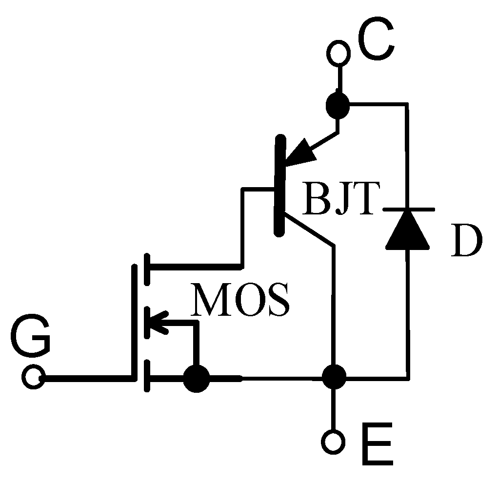
Figure 1. Network representation of the IGBT structure.
Energies 14 02372 g001
Figure 2. Network representation of a large-signal electrothermal model of the IGBT.
Energies 14 02372 g002
Figure 3. View of the tested device situated on the heat-sink.
Energies 14 02372 g003
Figure 4. Computed and measured output characteristics of the tested transistor operating at strong steering (a) and dependences of the case temperature on voltage VCE (b).
Energies 14 02372 g004
Figure 5. Computed and measured transfer characteristics of the tested transistor.
Energies 14 02372 g005
Figure 6. Computed and measured output characteristics at weak steering for the transistor operating without any heat-sink (a) and situated on the heat-sink (b).
Energies 14 02372 g006
Figure 7. Computed and measured dependences of the case temperature on output voltage at weak steering for the transistor operating without any heat-sink (a) and situated on the heat-sink (b).
Energies 14 02372 g007
Figure 8. Computed and measured waveforms of power lost in the tested transistor at switching-on (a) and switching-off (b).
Energies 14 02372 g008
Figure 9. Computed and measured dependences of the case temperature of the transistor operating in the circuit of a switch at the steady state on the maximum value of the collector current.
Energies 14 02372 g009
Publisher’s Note: MDPI stays neutral with regard to jurisdictional claims in published maps and institutional affiliations.