Abstract
Virtual Oscillator Control (VOC) is a promising technique that allows several inverters connected to a microgrid to naturally synchronize, without communication. However, the selection of the VOC parameters often require iterative or optimization procedures that render its practical use not straightforward. In this paper, this problem is overcome with the proposition of a novel methodology for determining the dead-zone type VOC parameters based on the describing function method. The methodology consists of a set of analytical equations that use as input data few basic electrical system parameters from the converter and from the microgrid, namely, the operating voltage and frequency ranges, besides rated power. The proposed set of equations is used to calculate the parameters required to control an inverter in voltage mode. The validity of the proposed approach is demonstrated in experiments that encompass different situations such as pre-synchronization, connection, and disconnection of a second inverter from a microgrid.
1. Introduction
Decentralized energy systems are becoming a promising alternative to the traditionally centralized model. This approach reduces the need for investments in transmission infrastructures, optimizes line losses, and assists in reactive compensation and voltage regulation [1,2]. At the same time, interest in using renewable energy for the energy matrix has increased considerably in recent years [3]. The use of photovoltaic panels, wind turbines, and other types of clean energy, besides the reduction of environmental impacts, has already become economically viable, especially in isolated places [4].
Observing this trend in the energy market, it is imperative to develop efficient and robust control strategies for power inverters operating in parallel, connected to the distribution system, or operating isolated from the grid. This type of structure is the basis for Parallel Connected Uninterruptible Power Supplies (PCUPS) and Micro Grid-based Electrical Power Systems (MGEPS) [5,6]. Important challenges in this architecture are related to the reduction or elimination of direct communication among inverters while ensuring stability and synchronization between generating units regardless of loads, regulating frequency and voltage, and providing load distribution according to the power of each generating device [7].
Parallel inverters synchronization methods can be divided into centralized, master/slave, distributed, and without communication (fully decentralized) [8]. This paper deals with the approach to control parallel inverters in a microgrid system without communication. The main advantage of this class of techniques is to avoid a common mode failure for the power distribution network associated with possible communication channel faults, thus improving the system overall reliability [9]. Usually the price to pay is the difficulty in distributing the power demand, since the load that each device must assume is unknown after unanticipated disconnections of faulted inverters.
Among methods of parallelism without communication, one of the most widely used is the Voltage and Frequency Droop Method (VFDM), or just Droop Control [10]. One of the first works on VFDM for converter control is presented in Chandorkar et al. [11], where transmission lines are considered inductive. VFDM then emulates the behavior of a synchronous generator controller, imposing an inverse relationship between frequency and active supplied power, while the exchanged reactive power is varied by voltage amplitude control. When the line cannot be considered purely inductive, the relationship between these variables needs to be modified accordingly [12]. In addition, when the line impedances to the load of each inverter are different, the method, as initially proposed, fails to properly distribute power between the generating units [12]. An approach used to mitigate the impacts of the two issues mentioned above is the use of a virtual impedance [13]. This impedance is designed to contribute to load distribution and can be chosen in such way that the equivalent impedance is inductive. Virtual impedances may even vary over time to accommodate changes in the electrical system [13].
Smooth operation of VFDM inverters is highly dependent on the way active and reactive power are estimated. Changing the underlying computation can improve the performance of a given implementation or lead to instability, as each estimation method adds different amounts of delay, usually associated with low-pass filters, to the control loop in each inverter. A simple way to obtain these power variables is presented in Andrade et al. [14].
In addition, previously developed synchronization methods that rely on estimated active and reactive power may exhibit slow convergence to the target power balance condition and usually need specific apparatus for the pre-synchronization and the power estimation procedures, such as phase-locked loops (PLLs). Other types of synchronization methods, e.g., those based on rotating (synchronous) reference frames, rely directly on PLLs to implement their strategies. In Wu et al. [15], it is shown the effects of PLLs on the converter stability, particularly how the interaction of PLLs with the grid/regulators can lead to instability.
These drawbacks have motivated the development of a new approach, the Virtual Oscillator Control (VOC), initially proposed in Torres et al. [16,17], with mathematical proofs for guaranteeing global asymptotic stability of the synchronization condition for symmetric electrical networks. To validate the theoretical developments, experimental results for the parallel operation of two inverters were presented, together with a pre-synchronization strategy to reduce the amplitude of transients at the time of connection of a new device in the electrical network [18]. In Johnson et al. [7,19], similar theoretical analysis and new experimental results were reported, and the term VOC was likely used for the first time.
Inverters controlled using the VOC technique usually have shorter settling times after load changes in comparison with other techniques. This is mainly because they do not depend on active and reactive power estimates commonly employed in other approaches. VOC is conceived considering time-domain variables [17], whereas conventional techniques are often based on phasors, taken as steady-state quantities or approximate mean values [20]. The steady state behavior of an inverter using VOC is similar to an inverter using VFDM [20,21]. Thus, it would be possible to use in the same network inverters controlled by both techniques. However, no work to date has explored this possibility. In Johnson et al. [21], the convergence time comparison is made between VOC and VFDM. It is possible to notice the superiority of the first method in the considered cases.
The first VOC studies have focused only on isolated microgrids, like the one shown in Figure 1. In more recent publications [22,23,24], a dispatchable VOC (dVOC) strategy was proposed. In this new approach, it is possible to set desired reference values for power injection that satisfy the power flow equations (steady-state condition). Nevertheless, the studied cases focus on isolated grids. Although Minghui Lu et al. [25] highlights that the VOC presented is grid-connected capable, neither stability nor synchronization studies in this context were presented. Furthermore, the Unified Virtual Oscillator Control (uVOC) is proposed in Awal et al. [26], which is built on the theoretical results of dVOC. The authors claim that uVOC can operate as Grid-Forming and Grid-Following with built-in fault protection, which allows a smooth transition between connected/isolated operation and protection of hardware against short circuits. The VOC can be used in conjunction with the active and reactive injection control to obtain dispatchable characteristics [27], this has advantage over the methods dVOC and uVOC because it is independent on the ratio of the line. Surprisingly, the VOC method has also been applied in direct current (DC) systems [28,29]. In Lin at al. [28], a current mode oscillator structure is used to control distributed active filters to attenuate the ripple in the DC line. On the other hand, in Duarte et al. [29] the VOC voltage output, after a coordinate transformation, is used to control DC/DC converters connected to a DC microgrid.
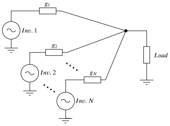
Figure 1.
Interconnected system with N inverters.
In most works about VOC, the underlying mathematical developments and methods used to choose appropriate parameters can render the widespread usage of this technique somewhat difficult. This paper proposes a novel strategy to determine VOC design parameters for application on parallel inverters connected to a microgrid (Section 2.2). Different from the work in Johnson et al. [21], this paper deals with dead-zone (or saturation) type oscillators, for which the parameter calculation method presented there is not applicable. In addition, the use of a saturation function instead of the cubic function, considered in that work, can potentially generate less third harmonic distortion for nominal load operation, if the parameters are chosen following our tuning methodology, by avoiding the saturation limits in this condition. Finally, the use of a piecewise-linear function (the saturation or dead-zone function, depending on the point-of-view) facilitates the discrete-time numerical implementation of the VOC strategy on Digital Signal Processors (DSPs) by the use of exact discretization methods for linear and time-invariant systems. The development presented in this paper could be used directly in applications such as in Ali et al. [27], Duarte et al. [29] and, with some modifications, in Lin at al. [28], with the benefits described above.
The proposed strategy consists of a set of analytical equations that use as input data only basic electrical parameters from the converter and from the microgrid, namely, the rated power and voltage and frequency ranges. It has the advantage over existing procedures to avoid the use of optimization, numerical solutions or graphical analyzes, and therefore significantly simplifies the VOC tuning process. In addition, a simple pre-synchronization strategy is presented (Section 3) to ensure smooth connection transients. Experimental results are presented in Section 4 to validate the proposed approach for a single-phase system. Other works has exploited the use of this type of controller on three-phase converters. The ideas presented in Johnson et al. [30] and Rosse et al. [31], concerning three-phase implementations, are compatible with the method presented here.
2. An Overview of The VOC Method
The concept of the VOC method is to emulate the dynamics of an oscillator through a power inverter. In the case of cooperation to feed the same load, this oscillator must have the property of naturally synchronizing with a unknown but finite number of several other power oscillators, that is, by construction the output voltages of all oscillators converge to the same quasi-sinusoidal oscillatory pattern, with low harmonic distortion, as a natural result of being connected to the same microgrid [17]. One of the possible oscillatory systems capable of presenting this property is shown in Figure 2, consisting of a filter and a current source controlled by a nonlinear voltage function, . The dynamic equations of this circuit are integrated by an appropriate numerical method, implemented in a DSP, which generates the voltage reference, , in that case equal to . This means that the components shown in Figure 2 are virtual ones, the reason why this method has been called Virtual Oscillator Control.
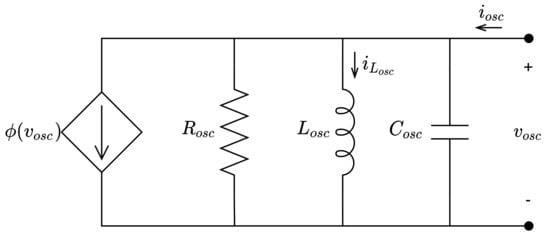
Figure 2.
Oscillator example, compatible with Virtual Oscillator Control (VOC) method and used in this work.
Considering the circuit in Figure 2, and applying Kirchhoff’s laws, one has that
where , , and is defined as the current flowing into the inverter. The controlled current source in Figure 2 behaves as a nonlinear resistor with piecewise constant non-positive resistance values, and it is able to inject current into the circuit. For limited amplitude oscillations, the function must also be bounded. The following saturation-like function is used:
where and are constant parameters to be designed.
Now, consider inverters controlled using this technique, with identical parameters, connected in parallel as shown in Figure 1. The theoretical justification for the synchronization of a unknown but finite number of power oscillators in a symmetric electrical network is related to the incremental passivity of the oscillators, together with the incremental passivity of the electrical network, in the sense briefly presented in Appendix A. Using this concept it was shown that a sufficient condition for synchronization, among others, is that
where is the passivity characteristic of the electrical network and is the passivity characteristic of the linear time-invariant (LTI) system (1) (see Section 2.1). In this case, all units in Figure 1 will synchronize naturally, sharing equally the load [17]. It is important to emphasize that inequality (3) is only a sufficient condition. In other words, even if the system violates this condition, it can still achieve synchronization in some cases. In Torres et al. [17], although the connection impedances were considered identical, the value of or the load characteristic (resistive/inductive) does not require modifications to the method structure, as opposed to VFDM.
2.1. Passivity Constraints on the Virtual Oscillator Design
Considering the LTI system presented in Equation (1), it is possible to define an energy storage function ([32] Definition 6.3) and compute its time-derivative as
As , one has that
and it can be concluded that the LTI system Equation (1) is Output Strictly Passive (OSP) ([32] Definition 6.3). Although the filter is passive, the nonlinear oscillator should not be, otherwise oscillations would not exist. The analysis of this condition can be performed by substituting in Equation (4), and recognizing that the system input is now ,
However, belongs to sector , so and Equation (5) can be rewritten as
Thus, the system will be OSP ([32] Definition 6.1) if
Moreover, making and , , in Eqation (1) leads to the conclusion that , , and therefore . This means that the system is zero-state observable ([32] Definition 6.5) and, from ([32] Lemma 6.7), the virtual oscillator, with , would be globally asymptotically stable, which is an undesirable condition. Therefore, one must have
where represents a safety margin for sustained oscillations when . So, the condition expressed in Equation (8) is a necessary one. This will be explored in the next section.
2.2. Practical VOC Parameters Selection
In Johnson et al. [21], the average oscillator models are used to obtain parameters for a Van der Pol oscillator with cubic function, considering a quasi-stationary operation condition. However, the described procedure can be laborious and somewhat non-intuitive. The use of cubic function nonlinearity has some disadvantages, as third harmonic generation (see Section 4.1). Besides, as reported in that work, an adaptation was required to eliminate an algebraic loop resulted from the use of approximate integration by means of the trapezoidal rule applied to discretize the smooth nonlinear differential equations. In order to overcome these drawbacks, a new approach for Voltage-Controlled Voltage Source Inverters (VCVSIs) control design, using VOC, is presented in this section. As described in Section 2, an oscillator with saturation nonlinearity will be used. The parameters are selected to reduce harmonic generation. As the saturation is a piecewise linear function, this allows the use of exact discretization of the linear time-invariant systems that are used in the DSP numerical implementation.
From Section 2, the necessary parameters to apply the VOC method are , , , , and . The parameters and are associated with the frequency of , while the amplitude is determined by the set of parameters , and . Furthermore, it is desirable to satisfy inequality Equation (3) such that must be chosen in order to guarantee both sustained oscillations and synchronization of inverters. From Equation (1), it is possible to infer that the current also influences the amplitude of the oscillations. In the event that , the load current will have little impact on voltage regulation. However, the more insensitive to the load current, the slower the synchronization process will become.
The describing function method is applied to the oscillator in Figure 2. For a single-input single-output (SISO) nonlinear system, represented by a linear system with a nonlinear function feedback with , there might be a periodic solution with a frequency and amplitude close to and a, if it is possible to solve the equation
where is the frequency response of the LTI system Equation (1) and is the describing function obtained for the nonlinear function ([32] Section 7.2). The expression in Equation (9) is known as the harmonic balance equation. For memoryless, time-invariant and odd functions, is real and can be calculated as
For the addressed problem, corresponds to the saturation function, Equation (2), with . In this case, the solution of Equation (10) is given by
where . By inspection we have
The transfer function for the system in Equation (1) is
Making , we have
Solving Equation (14) for it is found that the oscillation of the system, if it exists, must have an approximate frequency of
This result was already expected, as this is the central frequency of the bandpass filter shown in Figure 2. Solving now Equation (13) using Equation (17) we have
Therefore, if Equation (19) is met, according to the describing function method, the system represented by Equation (1), with feedback and with (disconnected from the electrical network), has a limit-cycle with amplitude a and frequency .
Although the describing function method is based on approximations and does not guarantee the existence of oscillations [32], the condition expressed in Equation (19) is consistent with that obtained in Equation (8). In addition, the method is useful in determining an approximate relation between the parameters , , , and the steady-state amplitude a. On the other hand, it also gives an approximate relation between the steady-state frequency and the parameters and .
In the previous analysis, was considered to be zero. However, this condition is not realistic, as the main objective of the inverter is to supply power to the grid. To partially circumvent this issue, it is possible to imagine that a load connected to the oscillator is actually part of it, changing the values of the internal impedances. In the special case where the load is a pure resistance, , the resulting equivalent resistance, , of the new oscillator would be the computed from the parallel connection between and . This means that regardless of the value of , the new value of the resistance of the oscillator would be less than the original value. Therefore, the load seen by the inverter when connected to the network has a direct impact on the oscillation condition of Equation (19). For a given value of , it is possible for the system to become asymptotically stable when connected to a load with a sufficiently small resistance value as pointed out in Equation (8). This will be associated with the maximum allowed active power output, or rated power. Furthermore, as already discussed, has an impact on the steady state amplitude, a, and must be used to define the minimum oscillation amplitude. Similarly, looking at Equation (17), inductive and capacitive loads will directly impact the ultimate system’s oscillation frequency.
To formalize the previous discussion, consider that the N inverters controlled by the VOC technique shown in Figure 1 are synchronized. Using the fact that these oscillators are incrementally passive, it can be inferred that all states between oscillators are equal in steady state. In this condition, the microgrid can be represented as shown in Figure 3. An equivalent circuit for a single inverter that is mathematically equivalent to the one in Figure 3 is shown in Figure 4.
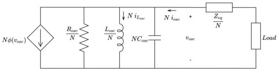
Figure 3.
Microgrid schematic representation after synchronization.
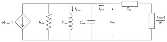
Figure 4.
Operating condition of one inverter after synchronization.
Neglecting the harmonics that can be generated by the load or by and considering that the system operates in steady state, that is, that phasor analysis can be applied, it is possible to decompose in a parallel or circuit in order to keep unchanged. In this case, , thus and . In addition, the power absorbed by the grid is given by and . Therefore, it is possible to determine the values of and as
Considering what has been presented so far, it is possible to describe an algorithm for choosing the VOC parameters. The input data are the minimum and maximum voltage values ( and ), nominal frequency and maximum frequency deviation ( and ), and inverter rated power ( and ).
First, we will define . The lowest bound is given by Equation (8), but for the new equivalent oscillator we must use and . When the inverter delivers nominal power, the oscillator voltage will be minimum. From Equation (20), . Considering the synchronization condition expressed in Equation (3) one has that
For simplicity, we choose as
This is a good choice because there is no need to deal with the grid structure or impedance to calculate . It is true that this does not guarantee synchronization, at least not without knowing the passivity characteristic of the electrical network. This represents a compromise between a simplified design procedure, which is the main purpose in this work, and the computation of a property that depends on the exact knowledge of the electrical network parameters but that would guarantee the satisfaction of the sufficient, and therefore strong, condition (3) for inverters synchronization. More information on the synchronization criteria and calculation are found in Torres et al. [17].
Using again the minimum voltage condition together with Equation (11) and Equation (18), for the value of to be equal to , must be greater than or equal to in Equation (11). The maximum voltage condition will happen for the no-load condition. This time must be equal to . Looking at the second part in Equation (11) we note that must be less than one, otherwise this equation has no solution. Thus must be less than . Again, for simplicity we choose
Using the minimum value allowed for will maximize , which helps filtering high frequencies created by . Moreover, for nominal load operation, the peak values of will be close to then , and practically no harmonic is generated by the oscillator.
After defining , and using the maximum voltage condition, it is possible to write the second part in Equation (11) as
where
The reactive power delivered by the converter can be associated with an inductive or capacitive current. If is inductive, the new inductance will be less than and the system frequency will be greater than the nominal frequency ; in this case, . On the other hand, with capacitive, will be greater than and the frequency will be less than the nominal frequency; in this case, . From circuit theory, it is known that
From Equation (17),
Applying these relations to Equations (27), (28) and (20), remembering that and , it is possible to write
As Equation (17) must also be satisfied with , it is not possible to satisfy Equations (29) and (30) simultaneously. However, must be maximized in order to minimize the filter pass band, given by
The lower the value of , the lower is the voltage harmonic distortion due to the nonlinear function . is calculated again starting from Equation (17) using Equation (29). The result is given by
must be chosen from . Comparing Equations (30) and (32) it can be concluded that , so (32) should be used. Once has been determined, the value of can be calculated using
We can summarize the presented method as follows:
- First, define the input parameters , , , , , and . Acquire the parameters from the inverter and from the microgrid (the inverter rated power and grid voltage and frequency). Define the aspects of power quality for your application. What is the minimal and maximum voltage amplitude and frequency allowed on your system? A good starting point is to use and and . Besides, some regulation or standard can be used to drive this choice [33].
- Use to calculate with Equation (23).
- Use to calculate with Equation (25).
- Use from previous step, , and to calculate and with Equation (26).
- Use , and to calculate with Equation (32).
- Use from previous step and to calculate with Equation (33).
In Section 4, an example is presented with the actual parameters extracted from an implemented test setup.
3. A Pre-Synchronization Strategy
Although it is shown that devices operating with VOC will achieve synchronization asymptotically regardless of the initial condition, the insertion of a new inverter in the network may cause unwanted transients [17]. With that in mind, it is important to perform the pre-synchronization of a device before connection. As shown in the next section, pre-synchronization allows the oscillator output voltage to be close to the line voltage before closing the connection switch. The voltage at the end of the line, however, is out of phase with the voltage of the inverters already in operation due to the connection impendance. Only after closing the switch final synchronization will take place.
The pre-synchronization method that is used in this work was inspired by Johnson et al. [7]. When a VOC inverter, with parameters obtained as described in Section 2.2, is inserted into the network, even if with large amplitude and phase differences, it quickly adapts and synchronizes with the rest of the system. The pre-synchronization process takes advantage of this feature. Thus, it is only required to emulate the converter operation before the switch is effectively closed. For this purpose, the circuit shown in Figure 5 is emulated in the that controls the converter.
Figure 5.
VOC schematic with pre-synchronization circuit.
As seen in the figure, a virtual source with a series resistor is used. The virtual source is a mirror of the voltage measured at the inverter terminals, where it will be connected. Therefore, the procedure consists of making the output current during the pre-synchronization period equal to
The virtual resistor, , must have a resistance value of the order of the equivalent connection resistance. If this parameter is unknown, can be used. The obtained value has little influence on the pre-synchronization result as long as the procedure described in Section 2.2 is followed. In any case, actual synchronization will follow after connection.
4. Results
4.1. Simulation Results
The main purpose of this section is to compare the dead-zone VOC, and design procedure introduced in this work, with the methodology presented in Johnson et al. [21]. It will be shown that less harmonic distortion, especially third harmonic, can be obtained by following the tuning methodology presented here, which relies on the use of a piecewise-linear nonlinear function, in comparison to the approach relying on a cubic nonlinear function. In addition, the reduction of harmonic content is achieved without harming dynamic behavior. In fact, it is possible to notice a reduction in synchronization time between devices that use this new approach. The simulation platform MATLAB® [34] was used along with Simulink® to obtain the results presented in this section.
First, it is important to understand the source of the harmonics related to both methods. The cubic function employed in Johnson et al. [21], considering a static application, will always generate the same relative third harmonic content because
and the ratio of the third harmonic amplitude to the amplitude of the fundamental component is always the same. Let be the relation between the third harmonic and the fundamental amplitude regarding only the static behavior of the nonlinear function, for the cubic function . For a saturation function the harmonic generation depends on how much an input sine wave is distorted, and this is regulated by the parameter. Remembering, the saturation function is defined as
The value assigned to from Section 2.2 is . The term is used because is compared with , which is an instantaneous voltage. The minimum voltage is reached with nominal load, so in this condition , and practically no harmonic distortion is generated by the oscillator. The worst case is the “no load” condition. In this scenario, the output voltage will be and the nonlinear function will cut the sine wave above . These voltages, and , are normally chosen to be close to the nominal voltage, thus only a small piece of the sine wave is removed. For saturation function the , where is defined by Equation (11), and is defined as
with Using the parameters from Table 1 and Table 2, the worst-case distortion rate for saturation function will be , that is, more than ten times better than the cubic function.

Table 1.
Input parameters from Reference Method (RM) [21].
Table 2.
Output parameters Proposed Method (PM).
However, all harmonics generated by the nonlinear function are attenuated by the RLC filter in the oscillator. Finally, the total harmonic distortion is obtained from the combination between harmonic source and filter attenuation in a feedback system—the oscillator. Therefore, let be the effective relation between the third harmonic and the fundamental amplitude. For a more detailed discussion we will present some simulation results. The simulation is configured such that there is only one oscillator connected, or not, to a load. The objective is to compare the harmonic distortion and frequency deviation obtained by using oscillators designed using our Proposed Method (PM) with oscillators designed using the Reference Method (RM) published in Johnson et al. [21]. The input parameters are taken from the RM, and they are replicated in Table 1.
Using these parameters on both selection guides generates the output parameters presented in Table 2 and Table 3. The last two parameters from Table 1 are used only in the RM.
Table 3.
Output parameters RM.
Note that the values obtained for the are quite different, and the value for the RM is approximately 19 times higher than for the PM. The larger capacitor in the RM is used to guarantee proper frequency regulation ([21] Equation (47)). With value, the effective third-to-first harmonic ratio can be calculated, for the RM ([21] Equation (41)). After the parameter definition, the two types of oscillators were implemented on simulation, on continuous and discrete-time domains. The integration step time for continuous-time simulation is and for the sample time in the discrete-time case. The simulation run for after voltage stabilization, and then the FFT algorithm was applied over the steady state portion of the data.
In the following, three simulation scenarios are presented, first with no load, second with nominal RL load, and third with nominal RC load. The results are respectively shown in Table 4, Table 5 and Table 6, where the acronyms “c.” and “d.” stand for continuous and discrete, respectively; “f” is the fundamental frequency; is the fundamental amplitude; and is the third harmonic amplitude.
Table 4.
No load simulation.
Table 5.
Nominal RL load.
Table 6.
Nominal RC load.
Note that in all cases the PM was better than the RM in terms of . In addition, among the investigated operating conditions, the RM had a small change, unlike the PM. This was expected, because the cubic function always generates the same , no matter the voltage amplitude. The calculated using Equation (41) from [21], is in accordance with the results. Moreover, the RM has a little, but noticeable, error on frequency regulation, and they are different for continuous and discrete implementation. To verify changing behavior related to load condition, another simulation was performed, now with of nominal RL load, and the result is presented in Table 7. There seems to be an almost linear relationship between and the load percentage when the PM is applied.
Table 7.
RL load 50% of nominal, (*) using and from RM.
The last two lines in Table 7 are related to the PM when and parameters from the RM are used. These values give a view of the impact of the oscillator structure on frequency regulation and harmonics generation. However, the higher the capacitance value and the lower the inductance, the more energy is stored in the oscillator. This will potentially impact the synchronization procedure. If there is a difference between the states of each oscillator, more energy needs to be dissipated in the network, and more time could be required for the synchronization. Even so, in the PM one has a considerable margin to increase the capacitance value when compared to the RM if some other performance target needs to be met. This gives space for future improvements in this designing guide.
In the sequence, a comparison between the PM and RM synchronization process will be presented. For the following simulations, two identical oscillators, with parameters from Table 2 and Table 3, are connected to an RL load, with 50% of nominal power, through two identical lines with and , as shown in Figure 1. The oscillators are constructed in discrete-time domain and the connection network in continuous-time domain, with and . Initially, only one oscillator is connected to the load, and after some time the second oscillator is added to the system. For the results presented in Figure 6 and Figure 7, the pre-synchronization procedure is not used. Instead, the initial conditions of each oscillator are calculated to generate a lag of between then. When the clock reaches the second oscillator is connected to the load through the RL line. As can be seen the oscillators behave similarly for the PM and RM.
Figure 6.
Synchronization of two oscillators designed with RM without pre-synchronization.
Figure 7.
Synchronization of two oscillators designed with PM without pre-synchronization.
For a more detailed analysis, the graph of Figure 8 was constructed, where the difference between the output voltages and output currents for each method is compared.
Figure 8.
Difference between output voltage and output current of each oscillator without pre-synchronization.
As can be seen in Figure 8, the PM reaches synchronization between oscillators faster than RM. Defining the settling time, , as the time it takes for a signal to fall below of its peak value, for PM and for RM , considering signal.
In order to check the total time of an oscillator on the network for entering into service, the next simulation also takes into account the pre-synchronization process following the technique presented in Section 3 with . The results are shown in Figure 9, Figure 10 and Figure 11. The initial conditions of each oscillator are calculated to generate a lag of 90° between then. When the clock reaches , the pre-synchronization process starts in the second oscillator, and at 30 ms mark it is connected to the load through the RL line. The pre-synchronization quickly changes the output voltage of the second oscillator for both methods, as seen in Figure 9 and Figure 10. Besides, the output current of oscillator increases smoothly after connection.
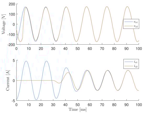
Figure 9.
Synchronization of two oscillators designed with RM with pre-synchronization.
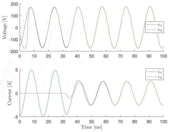
Figure 10.
Synchronization of two oscillators designed with PM with pre-synchronization.
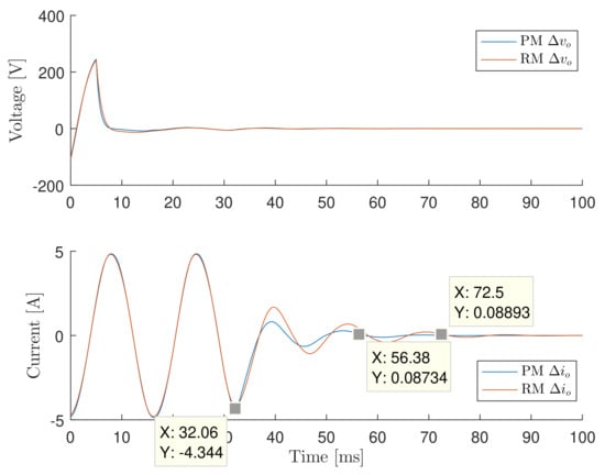
Figure 11.
Difference between output voltage and output current of each oscillator with pre-synchronization.
From Figure 11 it is possible to measure the settling time when the pre-synchronization is applied. In this case, this value will give an overview of the pre-synchronization and synchronization efficacy related with the VOC method applied. As in the previous case, the synchronization process for the PM is faster than in the RM. The values are for PM and for RM. For a quick comparison, Table 8 was constructed with the most important results presented in this section.
Table 8.
Results Summary.
4.2. Experimental Results
The VOC method was embedded in a single-phase commercial PV inverter [35] by firmware changing. The simplified schematic for the experiment is shown in Figure 12 and the assembly can be seen in Figure 13. The inverter output is connected to a coupling transformer, with a 1:1 ratio, that provides galvanic isolation between the input and output. The switch is used only for pre-synchronization strategy validation. When is closed, Inverter 2 automatically detects terminal voltage and starts the pre-synchronization procedure. Currents were measured with Hall effect current probes, while voltages were measured with differential probes. Data were stored in a four-channel digital scope, without any filtering. For reference, all relevant parameters are listed in Table 9. The two inverters have the same part numbers and are based on a H-brige IGBT (Insulated-gate Bipolar Transistor) topology with hard switching. The inductor and capacitor filters have and tolerances, respectively.
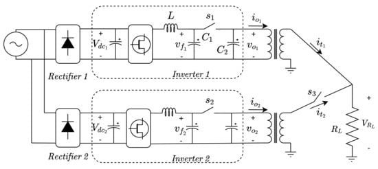
Figure 12.
Schematic of the laboratory-scale prototype for testing the VOC.
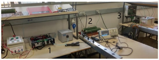
Figure 13.
Picture of the inverter assembly for testing the VOC algorithm: (1) Inverter nº. 1, (2) Set of resistive loads, and (3) Inverter nº. 2.
Table 9.
Parameters of the experimental setup.
The commands are made with triangular carrier unipolar PWM (). The duty cycle is defined as
All the calculations were made with fixed point math. To simplify implementation, the per unit system was used. Thus, before using the equations in Section 2.2, the input data must be converted using voltage and power bases. The used VOC parameters are presented in Table 9.
The values and are chosen symmetrically to as recommended on Section 2.2. The rated power of this inverter is . As the experiments will be performed with a resistive load, the values are chosen only to overcome the reactance from the transformers. A good starting point for is , but that limit could vary regarding some standard or equipment needs. We are choosing this parameter more tightly, , because we will deliver little reactive power. For the same value, a more restricted will increase , that normally leads to a longer synchronization time, regarding the same system. However, a bigger capacitance will help to reject more harmonics, because it reduces .
The test was conducted as follows. Initially, Inverter 1 was started. After stabilization, it was connected to the microgrid by closing switch . Then, switch was closed. The pre-synchronization procedure started automatically as soon as the rms value of exceeded . Subsequently, switch was closed to put inverter 2 into operation. After operating for a short period, switch was opened again so that Inverter 1 took over the entire load again. Results related to each of these steps are presented next. It must be noted that both inverters have the same firmware.
The first results are shown in Figure 14. This is related to pre-synchronization process of Inverter 2. As it can be seen, after a small transient the voltage in the inverter filter, , which is an image of VOC output voltage, replicates , except for a small lag. As will be seen below, this procedure ensures that the input transients of the inverters are well controlled.
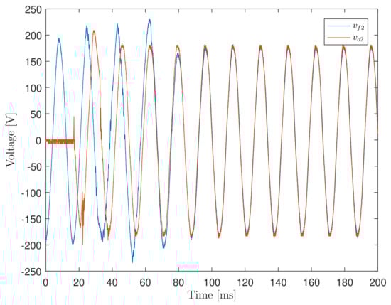
Figure 14.
Pre-synchronization process for Inverter 2.
Figure 15 shows the moment when the second inverter is connected to the microgrid. The measured voltages are and , as well as currents and (see Figure 12).
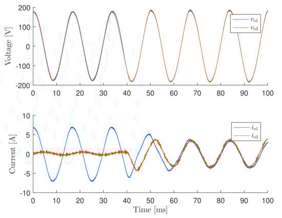
Figure 15.
Connection of the second inverter in the microgrid.
As seen in Figure 15, current quickly synchronizes with . In addition, a soft transient is achieved due to the pre-synchronization procedure. The difference between and is due to difference in transformers impedance. The more noticeable noise presented in is related to the higher sensitivity of the current probe 2. This noise comes mainly from common-mode electromagnetic interference generated by the inverter switching.
After some time in operation, switch was opened. The result is shown in Figure 16.
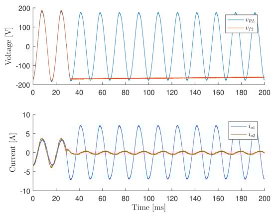
Figure 16.
Disconnection of the second inverter from microgrid.
The measured voltages are and . Once requested to disconnect, the inverter goes to a state where the PWM is deactivated, so the filter voltage after this event will tend to zero. The capacitor discharge, compared to the network frequency, is slow. This ends up generating the “continuous” signal seen in the graph of Figure 16. Another point to be highlighted is the reduction of the voltage in the load after the Inverter 2 is interrupted. This reduction is due to both the increase in losses in Inverter 1 and transformer and the reduction in the reference voltage generated by the virtual oscillator. Although the values of and were chosen symmetrically in relation to , this is not mandatory. The only restriction is that . In this way the value of can be chosen to compensate for possible losses in the inverter filter, if this is relevant in a specific application.
5. Conclusions
In this paper, a new method is proposed for determining the design parameters required for virtual oscillator control. In the the proposed method, all VCO parameters are directly computed with simple expressions that use as input data information that is readily available from the inverter and from the microgrid. The proposed method was implemented in a pair of converters that were set to operate as a microgrid in the laboratory. The obtained results demonstrate the validity of the method by investigating both the pre-synchronization process and the cooperative operation of both inverters in different operating conditions. The pre-synchronization ensures that the transients resulting from the insertion of a second inverter on an operating microcrid are smooth. This is essential for commercial applications, reducing the downtime of the device. It is also shown that the disconnection of inverter 2 does not create any trouble for the operation of inverter 1, which ultimately assumes all power that is delivered to the loads after disconnection. In future work, other scenarios need to be investigated, as well as pre-synchronization and cooperative operation. In addition, as presented in the results, the proposed method has potential advantages over the technique established in the literature. Following the design guide presented here, the dead-zone type VOC generates less third harmonic distortion and needs less time to synchronize when connected to a network.
Author Contributions
Conceptualization, D.A.C. and L.A.B.T.; methodology, D.A.C.; Resources D.I.B. and S.M.S.; Software, D.A.C.; validation, D.A.C., S.M.S., and D.I.B.; writing—original draft preparation, D.A.C., L.A.B.T., S.M.S., A.D.C., and D.I.B.; writing—review and editing, D.A.C., A.D.C., L.A.B.T., and S.M.S. All authors have read and agreed to the published version of the manuscript.
Funding
This research was funded by the Brazilian government agencies CAPES, FAPEMIG, and CNPQ.
Institutional Review Board Statement
Not applicable.
Informed Consent Statement
Not applicable.
Acknowledgments
The authors thank the Graduate Program in Electrical Engineering (PPGEE-UFMG) for supporting this research.
Conflicts of Interest
The authors declare no conflict of interest.
Appendix A. Incremental Passivity
The notion of incremental passivity is closely related to the usual concept of passivity representing relations among inputs, outputs, and storage functions depending on system states [32]. The incremental notion is instead associated with differences between inputs, outputs, and trajectories in state space. According to the work in [16], a generic dynamical system represented by
with inputs , outputs , and states , is said to be Incrementally Input Strictly Passive (IISP) (resp. Incrementally Output Strictly Passive (IOSP)) if there exists a positive definite incremental storage function and passivity characteristic (resp. and passivity characteristic ) such that the following respective inequalities hold, :
with such that the time-derivatives in the left-hand side are taken along the difference between the solutions and to (A1) starting, respectively, at with input and output , and at with input and output . Note that passivity of LTI systems implies the corresponding incremental passivity property, but this is not true for nonlinear systems.
One way to prove that the VOC method applied to power oscillators connected to symmetric networks will lead to the synchronization of the oscillators is to show that the differences between state trajectories from different oscillators will vanish asymptotically because of their incremental passivity properties, and the fact that they are in feedback with the incrementally passive interconnection electrical network. This gives an overall incrementally strictly passive system. A more in depth discussion of this topic can be found in Torres et al. [16,17].
References
- Chiradeja, P. Benefit of Distributed Generation: A Line Loss Reduction Analysis. In Proceedings of the IEEE/PES Transmission & Distribution, Conference & Exposition: Asia and Pacific, Dalian, China, 18 August 2005. [Google Scholar] [CrossRef]
- Huang, B.B.; Xie, G.H.; Kong, W.Z.; Li, Q.H. Study on smart grid and key technology system to promote the development of distributed generation. In Proceedings of the IEEE PES Innovative Smart Grid Technologies, Tianjin, China, 21–24 May 2012. [Google Scholar] [CrossRef]
- Ritchie, H.; Roser, M. Renewable Energy Charts. Available online: https://ourworldindata.org/renewable-energy (accessed on 15 October 2020).
- Li, Z.; Zang, C.; Zeng, P.; Yu, H.; Li, S. Fully Distributed Hierarchical Control of Parallel Grid-Supporting Inverters in Islanded AC Microgrids. IEEE Trans. Ind. Inform. 2018, 14, 679–690. [Google Scholar] [CrossRef]
- Alberto, L.; Silva, F.; Bretas, N. Direct methods for transient stability analysis in power systems: State of art and future perspectives. In Proceedings of the IEEE Porto Power Tech Proceedings (Cat. No.01EX502), Porto, Portugal, 10–13 September 2001. [Google Scholar] [CrossRef]
- Borrega, M.; Marroyo, L.; Gonzalez, R.; Balda, J.; Agorreta, J.L. Modeling and Control of a Master–Slave PV Inverter With N-Paralleled Inverters and Three-Phase Three-Limb Inductors. IEEE Trans. Power Electron. 2013, 28, 2842–2855. [Google Scholar] [CrossRef]
- Johnson, B.B.; Dhople, S.V.; Hamadeh, A.O.; Krein, P.T. Synchronization of Parallel Single-Phase Inverters With Virtual Oscillator Control. IEEE Trans. Power Electron. 2014, 29, 6124–6138. [Google Scholar] [CrossRef]
- Shanxu, D.; Yu, M.; Jian, X.; Yong, K.; Jian, C. Parallel operation control technique of voltage source inverters in UPS. In Proceedings of the IEEE 1999 International Conference on Power Electronics and Drive Systems. PEDS 99 (Cat. No.99TH8475), Hong Kong, China, 27–29 July 1999. [Google Scholar] [CrossRef]
- Patrick O’Connor, A.V.K. Practical Reliability Engineering; John Wiley and Sons Ltd.: Hoboken, NJ, USA, 2012. [Google Scholar]
- Vaidya, S.; Somalwar, R.; Kadwane, S.G. Review of various control techniques for power sharing in microgrid. In Proceedings of the 2016 International Conference on Global Trends in Signal Processing, Information Computing and Communication (ICGTSPICC), Jalgaon, India, 22–24 December 2016. [Google Scholar] [CrossRef]
- Chandorkar, M.; Divan, D.; Adapa, R. Control of parallel connected inverters in stand-alone AC supply systems. In Proceedings of the Conference Record of the 1991 IEEE Industry Applications Society Annual Meeting, Dearborn, MI, USA, 28 September–4 October 1991. [Google Scholar] [CrossRef]
- De Souza Azevedo, G.M. Controle e Operação de Conversores em Microrredes. Ph.D. Thesis, Univerdade Federal de Pernanbuco, Recife, Brazil, 2011. [Google Scholar]
- Guerrero, J.; GarciadeVicuna, L.; Matas, J.; Castilla, M.; Miret, J. Output Impedance Design of Parallel-Connected UPS Inverters With Wireless Load-Sharing Control. IEEE Trans. Ind. Electron. 2005, 52, 1126–1135. [Google Scholar] [CrossRef]
- Andrade, E.T.; Ribeiro, P.E.M.J.; Pinto, J.O.P.; Chen, C.L.; Lai, J.S.; Kees, N. A novel power calculation method for droop-control microgrid systems. In Proceedings of the 2012 Twenty-Seventh Annual IEEE Applied Power Electronics Conference and Exposition (APEC), Orlando, FL, USA, 5–9 February 2012. [Google Scholar] [CrossRef]
- Wu, H.; Wang, X. Design-Oriented Transient Stability Analysis of PLL-Synchronized Voltage-Source Converters. IEEE Trans. Power Electron. 2020, 35, 3573–3589. [Google Scholar] [CrossRef]
- Torres, L.A.B.; Hespanha, J.P.; Moehlis, J. Power supply synchronization without communication. In Proceedings of the 2012 IEEE Power and Energy Society General Meeting, San Diego, CA, USA, 22–26 July 2012. [Google Scholar] [CrossRef]
- Torres, L.A.B.; Hespanha, J.P.; Moehlis, J. Synchronization of Identical Oscillators Coupled Through a Symmetric Network With Dynamics: A Constructive Approach With Applications to Parallel Operation of Inverters. IEEE Trans. Autom. Control 2015, 60, 3226–3241. [Google Scholar] [CrossRef]
- De Azevedo Ávila, M. Operação em Paralelo e sem Comunicação de Sistemas UPS: Uma abordagem baseada em Passividade. Master’s Thesis, Universidade Federal de Minas Gerais, Belo Horizonte, Brazil, 2013. [Google Scholar]
- Johnson, B.B.; Dhople, S.V.; Hamadeh, A.O.; Krein, P.T. Synchronization of Nonlinear Oscillators in an LTI Electrical Power Network. IEEE Trans. Circuits Syst. I: Regul. Pap. 2014, 61, 834–844. [Google Scholar] [CrossRef]
- Sinha, M.; Dorfler, F.; Johnson, B.B.; Dhople, S.V. Uncovering Droop Control Laws Embedded Within the Nonlinear Dynamics of Van der Pol Oscillators. IEEE Trans. Control Netw. Syst. 2017, 4, 347–358. [Google Scholar] [CrossRef]
- Johnson, B.B.; Sinha, M.; Ainsworth, N.G.; Dorfler, F.; Dhople, S.V. Synthesizing Virtual Oscillators to Control Islanded Inverters. IEEE Trans. Power Electron. 2016, 31, 6002–6015. [Google Scholar] [CrossRef]
- Seo, G.S.; Colombino, M.; Subotic, I.; Johnson, B.; Gros, D.; Dorfler, F. Dispatchable Virtual Oscillator Control for Decentralized Inverter-dominated Power Systems: Analysis and Experiments. In Proceedings of the 2019 IEEE Applied Power Electronics Conference and Exposition (APEC), Anaheim, CA, USA, 17–21 March 2019. [Google Scholar] [CrossRef]
- Gros, D.; Colombino, M.; Brouillon, J.S.; Dorfler, F. The Effect of Transmission-Line Dynamics on Grid-Forming Dispatchable Virtual Oscillator Control. IEEE Trans. Control Netw. Syst. 2019, 6, 1148–1160. [Google Scholar] [CrossRef]
- Colombino, M.; Groz, D.; Brouillon, J.S.; Dorfler, F. Global Phase and Magnitude Synchronization of Coupled Oscillators With Application to the Control of Grid-Forming Power Inverters. IEEE Trans. Autom. Control 2019, 64, 4496–4511. [Google Scholar] [CrossRef]
- Lu, M.; Dutta, S.; Purba, V.; Dhople, S.; Johnson, B. A Grid-compatible Virtual Oscillator Controller: Analysis and Design. In Proceedings of the 2019 IEEE Energy Conversion Congress and Exposition (ECCE), Baltimore, MD, USA, 29 September–3 October 2019. [Google Scholar] [CrossRef]
- Awal, M.A.; Husain, I. Unified Virtual Oscillator Control for Grid-Forming and Grid-Following Converters. IEEE J. Emerg. Sel. Top. Power Electron. 2020, 1–1. [Google Scholar] [CrossRef]
- Ali, M.; Nurdin, H.I.; Fletcher, J. Dispatchable Virtual Oscillator Control for Single-Phase Islanded Inverters: Analysis and Experiments. IEEE Transactions on Industrial Electronics 2020, 68, 4812–4826. [Google Scholar] [CrossRef]
- Lin, J. Virtual Oscillator Control of Distributed Power Filters for Selective Ripple Attenuation in DC Systems. IEEE Trans. Power Electron. 2021, 36, 8552–8560. [Google Scholar] [CrossRef]
- Duarte, J.L.; Roes, M.; Xu, X.; Wang, F. Virtual Oscillator Control as Applied to DC Microgrids with Multiple Sources. In Proceedings of the 2020 IEEE 9th International Power Electronics and Motion Control Conference (IPEMC2020-ECCE Asia), Nanjing, China, 31 May–3 June 2020; pp. 2007–2011. [Google Scholar] [CrossRef]
- Johnson, B.B.; Dhople, S.V.; Cale, J.L.; Hamadeh, A.O.; Krein, P.T. Oscillator-Based Inverter Control for Islanded Three-Phase Microgrids. IEEE J. Photovoltaics 2014, 4, 387–395. [Google Scholar] [CrossRef]
- Rosse, A.; Denis, R.; Zakhour, C. Control of parallel inverters using nonlinear oscillators with virtual output impedance. In Proceedings of the 2016 18th European Conference on Power Electronics and Applications (EPE16 ECCE Europe), Karlsruhe, Germany, 5–9 September 2016. [Google Scholar] [CrossRef]
- Khalil, H.K. Nonlinear Systems; Prentice Hall: Upper Saddle River, NJ, USA, 2002. [Google Scholar]
- IEEE. IEEE Standard for Interconnection and Interoperability of Distributed Energy Resources with Associated Electric Power Systems Interfaces; IEEE Std 1547-2018 (Revision of IEEE Std 1547-2003); IEEE: Piscataway, NJ, USA, 2018; pp. 1–138. [Google Scholar]
- MATLAB Version 9.0.0.341360 (R2016a); The Mathworks, Inc.: Natick, MA, USA, 2016.
- Inverter Model: PHB 1500NS, Processing Unit: TMS320F28034; PHB Eletronica Ltda.: São Paulo, Brazil, 2018.
Publisher’s Note: MDPI stays neutral with regard to jurisdictional claims in published maps and institutional affiliations. |
© 2021 by the authors. Licensee MDPI, Basel, Switzerland. This article is an open access article distributed under the terms and conditions of the Creative Commons Attribution (CC BY) license (http://creativecommons.org/licenses/by/4.0/).