Article

Parasitic Loop Inductances Reduction in the PCB Layout in GaN-Based Power Converters Using S-Parameters and EM Simulations

1
Arts et Metiers Institute of Technology, Centrale Lille, Junia, University Lille, ULR 2697-L2EP, F-59000 Lille, France
2
CNRS, Centrale Lille, University Lille, F-59000 Lille, France
*
Author to whom correspondence should be addressed.
Energies 2021, 14(5), 1495; https://doi.org/10.3390/en14051495
Submission received: 27 January 2021 / Revised: 26 February 2021 / Accepted: 3 March 2021 / Published: 9 March 2021
(This article belongs to the Special Issue Wide Bandgap Semiconductors and Their Applications)

Abstract

:
Due to the high switching speed of Gallium Nitride (GaN) transistors, parasitic inductances have significant impacts on power losses and electromagnetic interferences (EMI) in GaN-based power converters. Thus, the proper design of high-frequency converters in a simulation tool requires accurate electromagnetic (EM) modeling of the commutation loops. This work proposes an EM modeling of the parasitic inductance of a GaN-based commutation cell on a printed circuit board (PCB) using Advanced Design System (ADS®) software. Two different PCB designs of the commutation loop, lateral (single-sided) and vertical (double-sided) are characterized in terms of parasitic inductance contribution. An experimental approach based on S-parameters, the Cold FET technique and a specific calibration procedure is developed to obtain reference values for comparison with the proposed models. First, lateral and vertical PCB loop inductances are extracted. Then, the whole commutation loop inductances including the packaging of the GaN transistors are determined by developing an EM model of the device’s internal parasitic. The switching waveforms of the GaN transistors in a 1 MHz DC/DC converter are given for the different commutation loop designs. Finally, a discussion is proposed on the presented results and the development of advanced tools for high-frequency GaN-based power electronics design.

1. Introduction

The requirements of high power density and compact power electronics systems have increasing importance in recent years in embedded systems, such as automotive, aerospace. Increasing the switching frequency of power converters is a notorious solution to reduce the size and weight of passive devices. However, switching losses in active devices will increase proportionally with frequency, leading to a negative impact on converter efficiency and size of cooling systems. Consequently, there is a need of new power devices with better suitability for high-frequency operation than their silicon counterparts. In this context, Gallium Nitride (GaN) High Electron Mobility Transistors (HEMTs) are attractive technologies for efficient power conversion at frequencies higher than the megahertz due to their higher electron mobility and lower interelectrode capacitances than silicon components [1]. Several recent works have brought to light the great potential of GaN power devices for high power density converter design [2,3,4,5,6].
Although GaN transistors are the key to high-frequency power conversion, their switching speed in the nanosecond range generates high voltage spikes and ringing by exciting parasitic elements in the commutation cells. Consequently, it is necessary to minimize the parasitic inductances of commutation loops in order to reduce power losses as well as high-frequency electromagnetic interferences (EMI) [7]. As shown in Figure 1, the commutation loop inductance has two main origins: the internal interconnections in devices packages and the external interconnections, for example, on a printed circuit board (PCB tracks).
Technological improvements have been achieved in recent years to minimize parasitic inductances in GaN transistors packaging, leading to a drastic reduction in the component sizes [8,9]. The monolithic integration of the GaN power transistor and its gate driver, minimizing the gate loop inductance, contributes to modern challenges for highly efficient high-frequency power conversion [10,11]. For low power applications, previous works have shown the possibility of a monolithic integration of the full power stages [12,13]. However, for higher power applications, larger parasitic inductance due to interconnections between GaN devices and the DC link capacitor is still present in classic commutation loop configuration. Previous works have highlighted that the proper design of a commutation loop on a PCB can reduce the resulting parasitic inductance [14,15,16].
The determination of commutation loop inductance over a wide frequency range enables an improvement in the modeling of component behavior in high-frequency power converters. Thus, power losses in devices and electromagnetic interferences (EMI) can be better predicted. A method to determine the loop inductance using an analytical model based on the Biot–Savart formula is presented in [17]. Other works have estimated the parasitic inductance using numerical methods, such as Partial Element Equivalent Circuit (PEEC) or the Method of Moments (MoM) [18,19]. However, a frequency-dependent model of commutation loop inductance including power devices usable in an electromagnetic (EM)/circuit simulation environment is needed to perform accurate predictions of switching waveforms. Furthermore, to date, an experimental validation of the parasitic loop inductance modeling has not been proposed.
This work proposes a frequency-dependent inductance model of a commutation cell including GaN transistors on the PCB for high-frequency power converter design. The proposed model is based on EM/circuit co-simulations and an experimental extraction of the parasitic inductance including GaN device packaging effects using S-parameter measurements over the frequency range 1–500 MHz. The S-parameters method is an accurate microwave measurement technique showing accuracy to extract parasitics in power devices [20,21,22,23]. In this study, it is proposed to extend existing techniques to the characterization of parasitic elements in a commutation cell. A calibration procedure and different 2-port measurement techniques are presented in order to obtain the best accuracy in the considered frequency range. The obtained experimental results are then used to validate the developed models but also to adjust the GaN transistor intrinsic inductance. Two different PCB designs of the commutation loop are studied: a lateral structure (single-sided) and a vertical structure (double-sided) involving high inductive coupling between PCB tracks [24]. Both designs are characterized by S-parameters and modeled using Advanced Design System (ADS®) software. Experimental switching waveforms in a 1 MHz DC/DC converter are given for both PCB layouts of the commutation loop. The advantages of the proposed commutation loop modeling for the development of high-frequency power converter design tools are finally discussed.

2. Commutation Loop Characterization Method

2.1. Description of the Studied Commutation Loop

In this work, it is proposed to extract the parasitic inductance of a commutation loop in a wide frequency range. Figure 1 gives a schematic representation of the considered commutation cell. It is composed of two GaN transistor GS66502B 650 V, 7.5 A and a DC bus ceramic capacitor of 100 nF in 0603 package, which withstands 630 V. All the components are connected on a printed circuit board with 35 µm of copper thickness and 400 µm of FR4 height. Referring to Figure 1, the characterized parasitic loop inductance L l o o p is given by (1).
L l o o p = L e x t + L D T 1 + L S T 1 + L D T 2 + L S T 2 ,
where L e x t is the external inductance due to PCB interconnects; L D T 1 ,   L D T 2 ,   L S T 1 ,   and   L S T 2 are the drain and source intrinsic access inductances of the GaN devices.
In the first approach, the equivalent series inductance (ESL) of the DC bus capacitor is not considered in the commutation loop inductance. However, this parameter should be added in the simulation of the whole system.

2.2. Calibration Procedure

S-parameter characterization has demonstrated a good accuracy to extract low inductance values in the nanohenry range up to the gigahertz [20,21]. In order to perform accurate S-parameter measurements on a PCB commutation loop, test fixtures associated with a specific calibration method were developed. Thus, it is proposed to design 50 Ω microstrip transmission lines on PCB ended by 50 Ω Subminiature A (SMA) connectors to connect the vector network analyzer (VNA) for S-parameter characterization. The geometry of the transmission lines is determined using the classic formula from [25] and given by (2).
Z C T L = 60 0.475   ε r + 0.67 ln ( 5.98   h 0.8   w + t ) ,
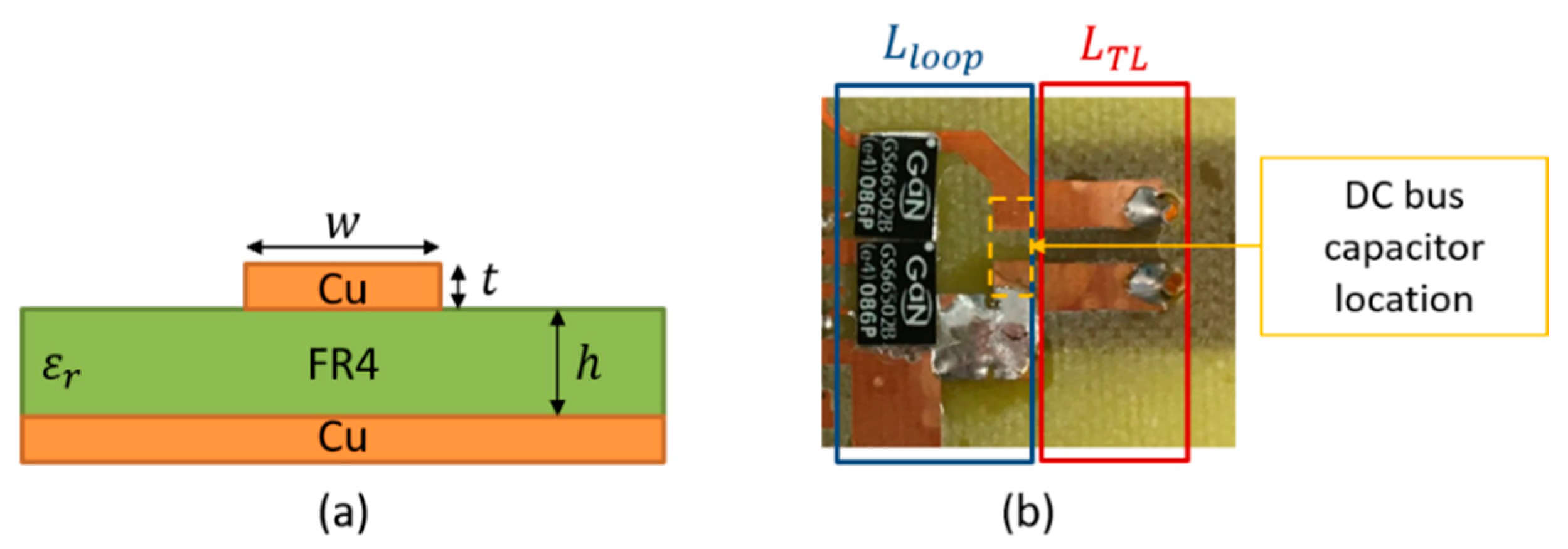
where Z C T L is the characteristic impedance of the transmission line (50 Ω). As represented in Figure 2a, ε r = 4.2 is the relative permittivity of FR4, h is the thickness of the dielectric, w is the width of the line and t is the conductor thickness. A ground plane is located on the PCB bottom side.
Figure 2b gives a first design of the commutation loop in a lateral configuration on PCB connected to transmission lines for the 2-port S-parameter characterization. According to Figure 2b, the measured inductance is given by (3), where L T L is the inductance induced by the transmission lines.
L m e a s = L l o o p + L T L ,
In order to determine the loop inductance L l o o p , it is necessary to obtain accurate values of L T L over the studied frequency range. Thus, the proposed method can be divided into three different steps. Figure 3 gives the organizational chart of the proposed method. First, S-parameter measurement is performed on fixture 1 which consists of two transmission lines connected without any coupling between lines. This measurement is compared with the EM simulation in ADS software permitting us to adjust the modeling of the SMA connectors. Then, the inductance L T L of the transmission lines in fixture 2 is determined by simulation over the characterization frequency range. A second step consists in extracting the inductance of a PCB loop with a design close to those of the commutation loop. Then, the experimental results are compared with simulations. Once this second step is validated, it consists in modeling the drain–source inductance added by the GaN devices packaging. The last part of the work is performing S-parameter measurement on the commutation loop including the GaN devices and comparing experimental results with EM simulations.
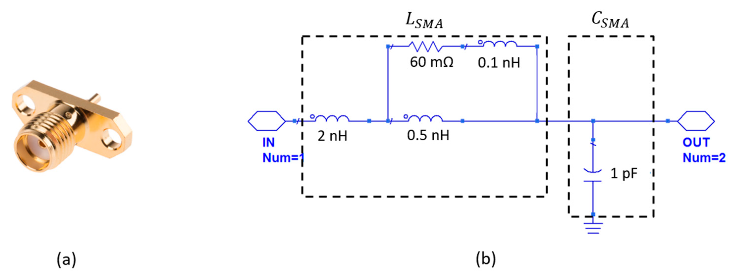
In order to obtain accurate modeling of the SMA connectors, a “Thru” S-parameter measurement was performed on fixture 1, shown in Figure 3, from 1 to 500 MHz. An EM model was obtained from the PCB layout of the test fixture using the setup given in Table 1. A classical LC modeling ( L S M A ,   C S M A ) of the SMA connector can be determined from the well-known Formulas (4) and (5) adapted to a coaxial connector [26,27], where µ 0 is the permeability constant, ϵ 0 is the permittivity constant, ϵ r is the relative permittivity of dielectric in connectors ( ϵ r = 2 ), a is the inner diameter and b is the outer diameter and l is the length of the connector. This modeling was further improved by considering the observed frequency dependence of the inductance. The modeled SMA connector is presented in Figure 4a, and the proposed equivalent circuit for this connector is given in Figure 4b.
L S M A = µ 0 2 π ln ( b a ) l ,
C S M A = 2 π ϵ r ϵ 0 ln ( b a ) l ,
Figure 5a shows the experimental and simulation setups. The measured and simulated inductance of fixture 1 is compared in Figure 5b. It can be noted that measurements are noisy below 10 MHz due to the low impedance values. The relative error between measurement and simulation is less than 3% in the frequency band 10–500 MHz. Once the SMA model and the EM simulations are set off, the inductance, L T L , of the fixture 2 is determined by simulation over the considered frequency range.

2.3. S-Parameter Measurement Techniques

Extracting the low parasitic values in GaN-based commutation loops requires accurate S-parameter measurement techniques. The three different ways to measure an impedance Z 0 using S-parameters are presented in Figure 6. The classic 1-port S-parameter reflection in Figure 6a has good accuracy to measure impedances close to 50 Ohms. However, the measurement error increases rapidly when the impedance differs from 50 Ohms. In order to perform accurate extraction of a low inductance over a wide frequency range, 2-port S-parameters techniques, such as Shunt-Thru and Series-Thru (in Figure 6b,c, respectively), are preferred to the 1-port measurement [28,29]. It has been shown that when the impedance value is below 50 Ω, the Shunt-Thru measurement demonstrates the best accuracy. By opposition, when the impedance values are higher than 50 Ω, the Series-Thru technique gives the best results. As the impedance of an inductance increases with the frequency, the Shunt-Thru method is the most suitable for low-frequency measurements, while Series-Thru is most suitable for high-frequency characterizations. Theoretically, considering inductance values around 10 nH or lower, the Shunt-Thru technique is the most accurate over the complete characterization frequency range in this work. However, in Shunt-Thru configuration, a T-SMA connector is needed to connect the 2 ports together. This added connector increases the inductance of the measurement setup, possibly increases the measurement error and complicates the calibration process. Thus, both Shunt-Thru and Series-Thru methods are compared in this work.
The Series-Thru S-parameter measurement setup and its equivalent circuit are presented in Figure 7. In this equivalent circuit, Z o p e n is the open impedance due to capacitive coupling between lines and ground plane, Z T L is the impedance of both transmission lines obtained according to the calibration procedure described in Section 2.2 and Z 0 is the characterized impedance. After transforming the measured S-parameter matrix [ S S e T ] into admittance parameters [ Y S e T ] , the impedance Z 0 can be determined using Equation (6). Considering Z 0 is purely resistive and inductive, the desired inductance value L 0 is obtained using Equation (7).
Z 0 = 1 Y 21 S e T Z T L ,
L 0 = I m ( Z 0 ) ω ,
The Shunt-Thru S-parameter measurement setup and its equivalent circuit are presented in Figure 8. After transforming the measured S-parameter matrix [ S S h T ] into impedance parameters [ Z S h T ] , the impedance Z 0 can be determined using Equation (8). As previously mentioned, considering Z 0 is purely resistive and inductive, the desired inductance value L 0 is obtained using Equation (7).
Z 0 = 1 1 Z 21 S h T 2 Z o p e n Z T L ,
The impedance Z o p e n can be determined by a first measurement without connecting the ground termination shown in Figure 8a.

3. Characterization and Modeling of a Lateral Commutation Loop Inductance

In this section, it is proposed to characterize the inductance of a lateral PCB loop and a lateral commutation cell including the GaN transistors in the loop. The followed methodology is presented in Figure 3. For each commutation loop, S-parameter measurements and simulations were performed and results were compared. For experimental characterizations, the calibration procedure described in Section 2 was used. For simulations, EM models of the loops were developed using ADS Momentum®. In order to improve the simulation results on the complete commutation loop, a method is proposed to obtain an equivalent EM modeling of the GaN transistors packaging.

3.1. Inductance of a Lateral PCB Loop

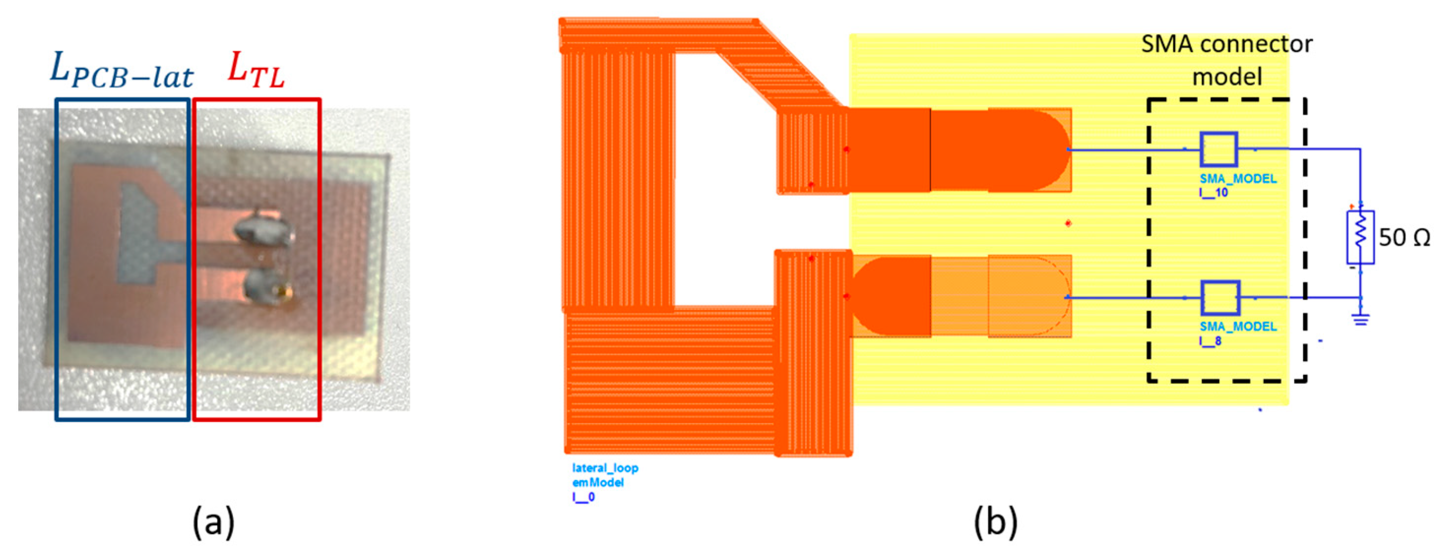
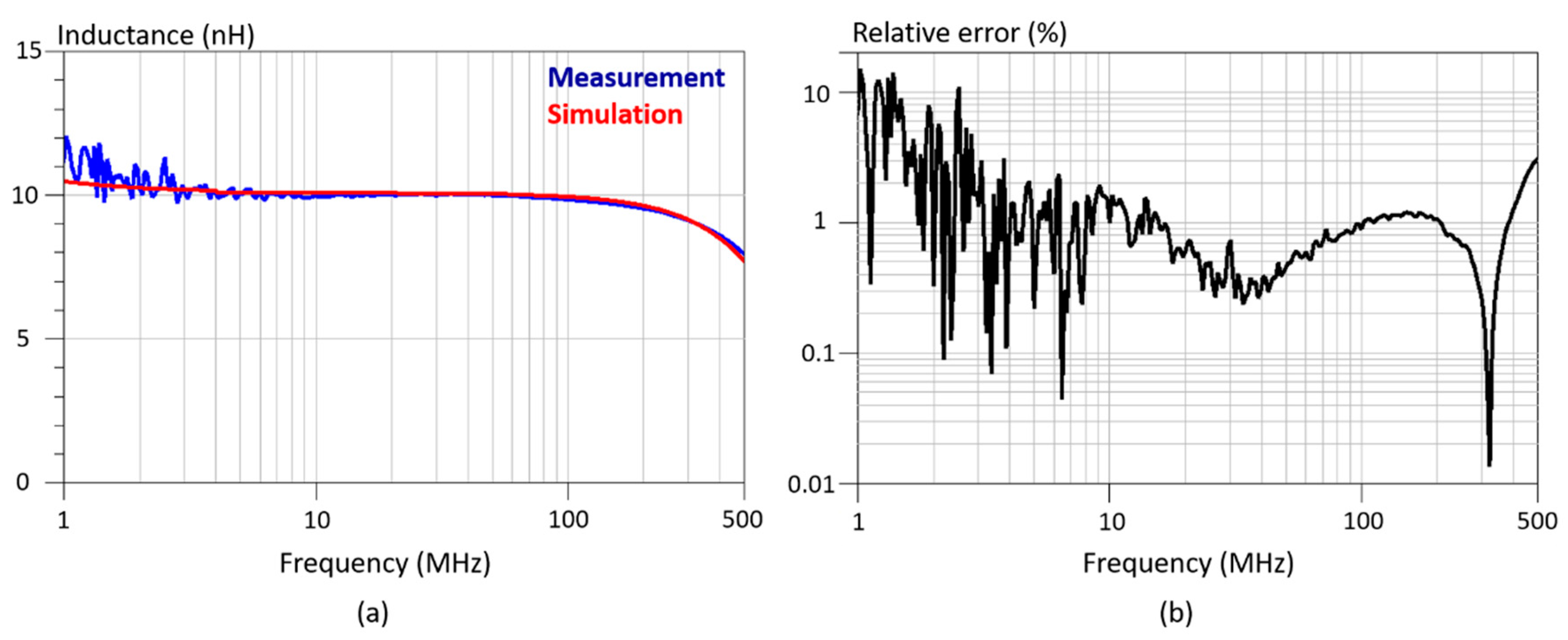
In order to validate the S-parameter characterization procedure, the PCB loop shown in Figure 9a was designed with equivalent sizes to the lateral commutation loop shown in Figure 2b. An EM modeling of the PCB layout was performed in ADS Momentum using the setup given in Table 1. Figure 9b presents the corresponding simulation setup implemented in the software. Using the calibration procedure described in Section 2.2 and Equations (6)–(8), the inductance of the lateral PCB loop L P C B l a t can be determined. Figure 10a gives the inductance values extracted from measurement and simulation in the frequency band 1—500 MHz. A good agreement between experimental and simulated results with less than 10% of relative error over the frequency range is shown in Figure 10b.

3.2. GaN Transistors Drain–Source Inductance

The determination of the drain–source inductance of the GaN transistors is required in order to obtain an accurate estimation of the commutation loop inductance by simulation. This inductance is a combination of internal parasitic inductance due to the packaging and inductive effects of devices footprints on PCB. Therefore, in this work, it is proposed to develop an EM model of the drain–source inductance based on the characterization of the GaN device soldered on PCB.
A 2-port S-parameter measurement was performed on the GaN transistor using specific characterization fixtures on PCB as detailed in [20]. The experimental setup is given in Figure 11a. It can be noted that the thickness of PCB is 1.6 mm for this fixture. The Cold FET measurement technique was used to create a resistive and inductive path between drain and source of the device [30]. The equivalent circuit of the transistor in Cold FET conditions is presented in Figure 11b, where C g and G g are the capacitance and conductance of the gate diodes, and R c h is the channel resistance depending on V G S voltage. R G , R D and R S are the access resistances and L G , L D and L S are the parasitic inductances at each terminal of the device.
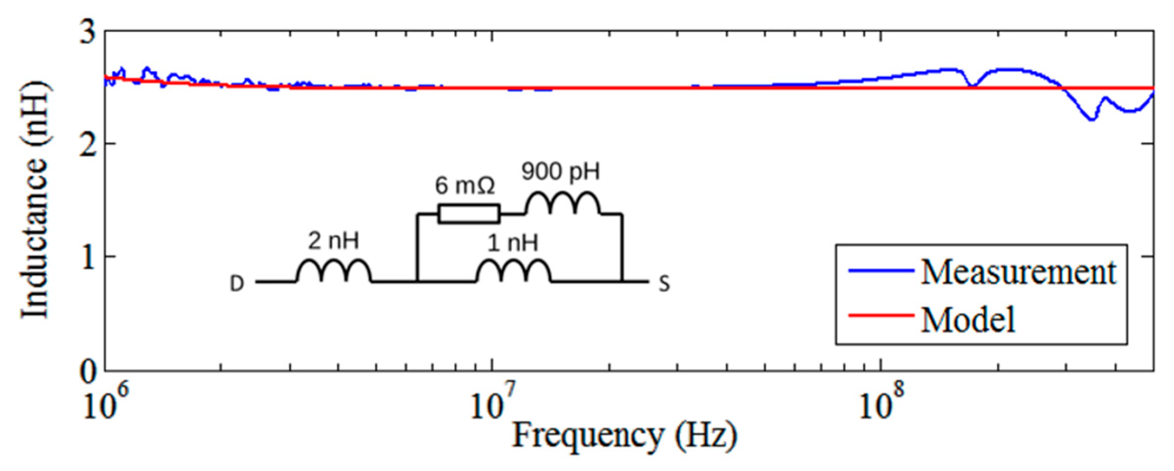
After calibration, the obtained S-parameters in the plane of the device [ S T ] were transformed into Z-parameters [ Z T ] . According to the circuit shown in Figure 11b, the drain–source inductance, L D S T , can be determined using Equation (9). Measurements were performed in the frequency band 1–500 MHz at V G S = 6 V using Bias Tees. Experimental results and a first modeling using R-L circuits are given in Figure 12. It was observed that the results converge to an equivalent drain–source inductance of 2.5 nH in the frequency range 1–500 MHz.
L D S T = L D + L S = I m ( Z 22 T ) ω ,
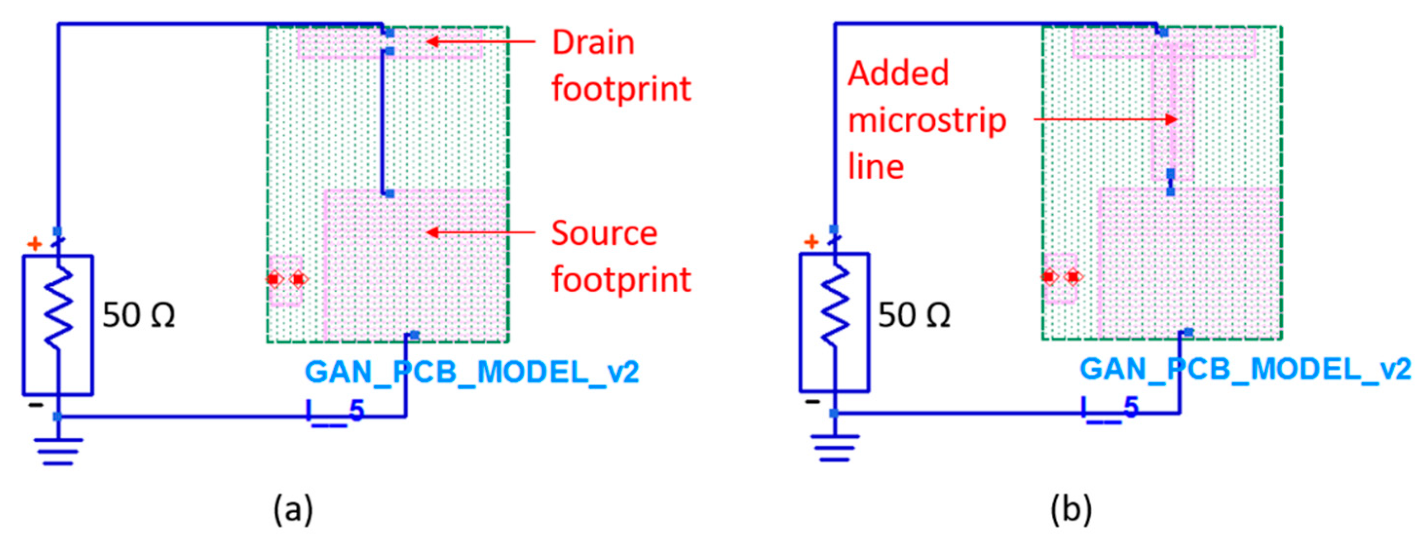
Accurate modeling of the commutation loop requires an EM modeling of the equivalent drain–source inductance. A first simulation, presented in Figure 13a, analyzed the inductance due to the PCB footprint of the device, called L P C B T . Simulation results given in Figure 14 show that there is a difference of about 20% between L P C B T and the measured drain–source inductance L D S T . It is assumed that this difference comes from a parasitic inductance due to interconnections in the device packaging.
To adjust the EM modeling with experimental results, a piece of microstrip line was added into the drain to source path. The microstrip line inductance, L m s , was determined using Equation (10) derived from [31,32], where L is the length of the line. The inductance is given in µH. L , w and h are in inches in the formula. The simulation model with the added microstrip line is presented in Figure 13b. Simulation results with this improved modeling give a maximal difference of 2% according to experimental results, as shown in Figure 14.
L m s = 0.00508   L ( ln ( 2 L w + h ) + 0.5 + 0.2235 ( w + h L ) ) ,

3.3. Inductance of a Lateral Commutation Loop Including GaN Devices

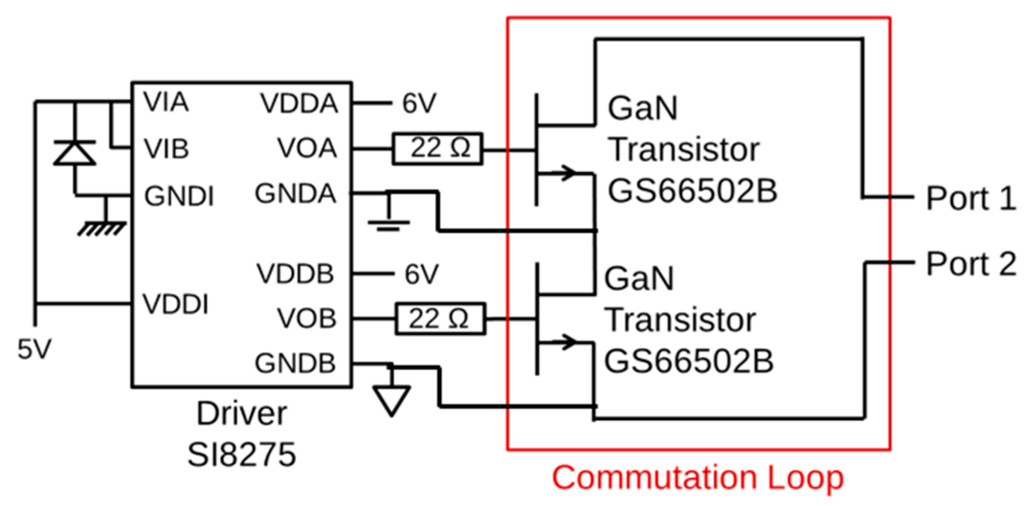
The experimental extraction of the commutation loop inductance is only possible if both GaN transistors are in conductive states. As detailed in Section 3.2, the drain–source path is resistive and inductive when GaN devices are in Cold FET conditions. Therefore, it is proposed to bias both transistors at V G S = 6 V during measurements using an auxiliary circuit, as shown in Figure 15. The driver SI8275 allows us to apply control signals to the transistors in a half-bridge configuration with separated ground references.
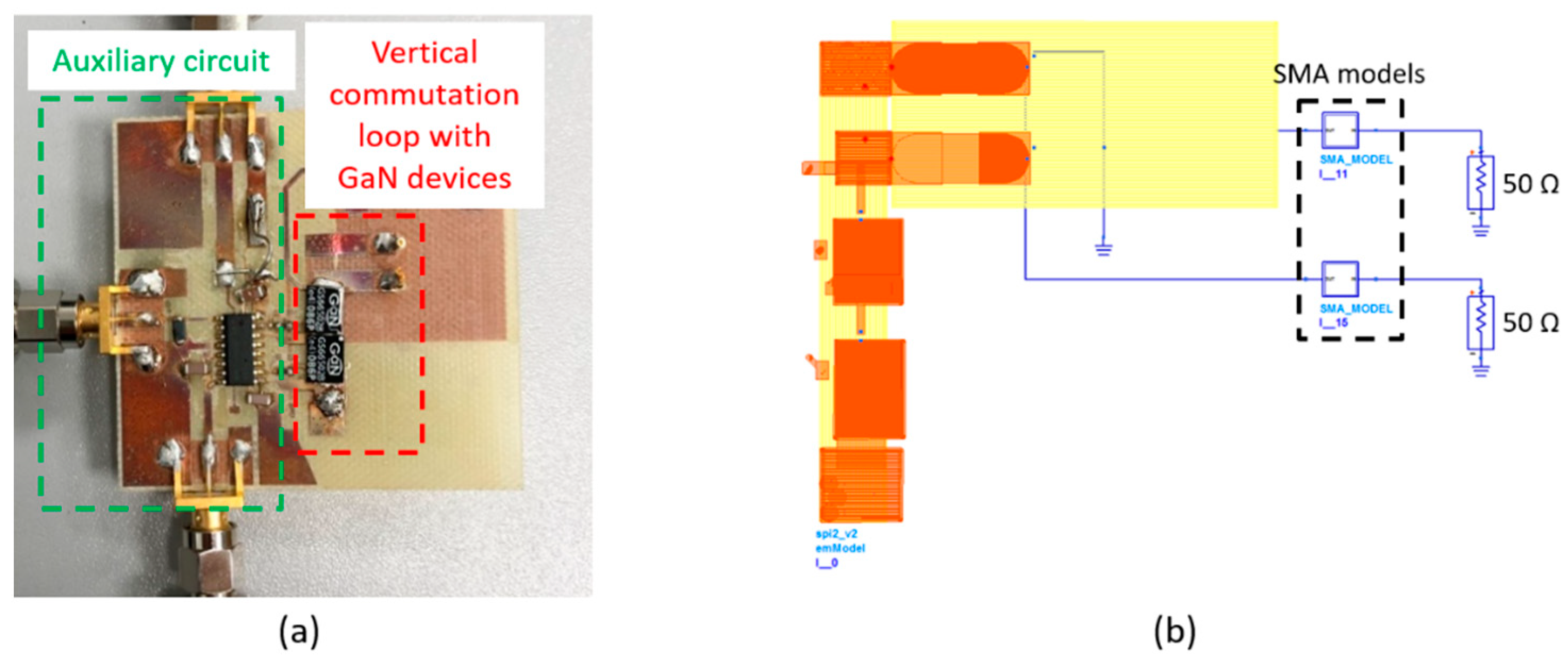
Figure 16a presents the experimental characterization circuit. Using the calibration procedure described in Section 2.2 and Equations (6)–(8), the inductance of the lateral commutation loop L l o o p l a t can be determined. An EM modeling of the PCB layout was performed in ADS Momentum using the setup given in Table 1. The EM models of the GaN devices developed in Section 3.2 were added to the simulation. Figure 16b presents the corresponding simulation setup in the software.
Figure 17a gives measurement and simulation results of the commutation loop inductance in the frequency band 1–500 MHz. A good agreement between experimental and simulated values globally less than 10% of relative error is shown in Figure 17b. It can be noted that due to the auxiliary circuit in the test setup, measurement results are noisier than those presented in Section 3.1. This can impact the calculation of the relative error.

4. Characterization and Modeling of a Vertical Commutation Loop Inductance

In this section, the proposed method was applied to an improved design of the commutation loop. The vertical configuration of the commutation loop presented in Figure 18 allows us to reduce the loop inductance due to the magnetic flux where opposite current directions occur in the top and bottom layers [14].
Although the inductance of a lateral commutation loop can be accurately simulated using a simple circuit simulation, the vertical commutation loop simulation is more complex due to high inductive couplings and via holes. Therefore, EM simulations become necessary. The GaN transistors will have an impact on the inductive coupling between layers; therefore, an experimental characterization of the vertical loop inductance including GaN devices is required to obtain accurate results. First, the extraction of a PCB vertical loop inductance was studied. Then, the method was applied to the complete commutation loop including the GaN transistors.

4.1. Inductance of a Vertical PCB Loop

The vertical PCB loop shown in Figure 19a was designed according to sizes of GaN transistors in the vertical commutation loop represented in Figure 18. As previously described, transmission lines were added for S-parameter characterizations. An EM modeling of the PCB layout was performed in ADS Momentum using the setup given in Table 1. Figure 19b presents the corresponding simulation setup in the software. Using the calibration procedure described in Section 2.2 and Equations (6)–(8), the inductance of the vertical PCB loop L P C B v e r can be determined. Figure 20a gives the extracted inductance by measurement and simulation in the frequency band 1–500 MHz. A good agreement between experimental and simulated values with less than 10% of relative error in the frequency range 10–500 MHz is shown in Figure 20b. Measurements are noisy below 10 MHz due to low impedance values.

4.2. Inductance of a Vertical Commutation Loop Including GaN Transistors

The experimental extraction of the vertical commutation loop inductance with the GaN transistors is based on the same circuit shown in Figure 14. Figure 21a presents the experimental characterization circuit. Using the calibration procedure described in Section 2.2 and Equations (6)–(8), the inductance of the lateral commutation loop L l o o p v e r was determined. An EM modeling of the PCB layout was performed in ADS Momentum using the setup given in Table 1. The EM model of the GaN devices developed in Section 3.2 was added to the simulation. Figure 21b presents the corresponding simulation setup in the software.
Figure 22a gives the vertical commutation loop inductance values extracted from the measurement and simulation in the frequency band 1–500 MHz. A good estimation of the commutation loop inductance with globally between 20 and 30% of relative error in the whole frequency range between measurement and simulation is shown in Figure 22b. As for the lateral commutation loop, due to the auxiliary circuit in the test setup, measurement results are noisier than those presented previously. This can impact the relative error calculation. Furthermore, the characterization of a vertical commutation loop is more complex than the lateral configuration due to strong inductive couplings and the presence of via holes. One explanation for the higher relative error can be the copper thickness in the metallized vias set off in simulation, which is only an estimation. Accurate modeling of the via holes should be investigated in future works.
Table 2 shows the experimental and simulated inductance values at 10 and 100 MHz for each characterized loop including the GaN devices. It was observed that the proposed method enables a good estimation of the commutation loop inductance in the different tested configurations and over a wide frequency range. As shown in Table 2, the vertical design of the commutation loop allows us to reduce the parasitic inductance by approximately a factor of 3. Measurement and simulation results are in good agreement.

5. Analysis of GaN Transistors Switching Waveforms for Two Commutation Loops

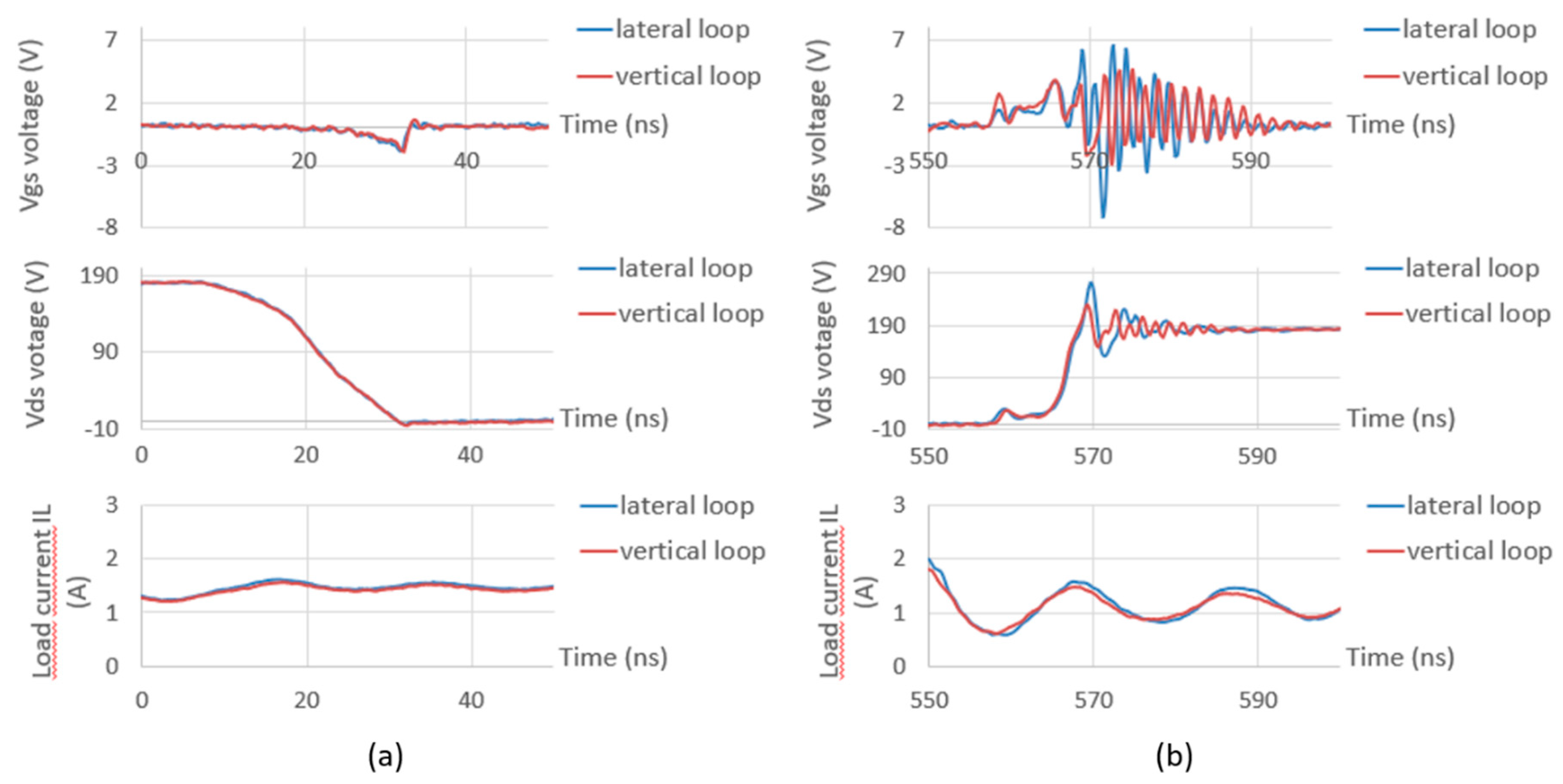
In this section, it is proposed to analyze the effect of the parasitic inductances on switching waveforms of the GaN transistors. The test circuit is presented in Figure 23a. The DC bus voltage is 200 V, and the switched current is about 2 A. The switching frequency is 1 MHz. The gate–source voltage, V G S , and the drain–source voltage, V D S , of the low side transistor T 2 were measured using optically isolated voltage probes IsoVu® (TIVM1 and TIVH08) with a bandwidth of 1 GHz. The current in the transistor was not measured because the introduction of current probe would modify the parasitic inductance of the switching loop. Figure 23b gives the switching waveforms during the measurement. The realization of both converters with lateral and vertical loop are presented in Figure 24a,b, respectively, and the measurement setup is given in Figure 24c. The experimental V G S and V D S waveforms at turn-off and turn-on of the transistor T 2 are given in Figure 25a,b, respectively. No notable difference was observed at turn-on transition. However, it can be observed that the overvoltage at turn-off is greatly reduced using the vertical design of the commutation loop. Experimental results give 50% overvoltage with the lateral commutation loop and 27% overvoltage with the vertical configuration. Voltage ringing frequencies at turn-off were estimated to 240 MHz with the lateral loop and 600 MHz with the vertical loop. The V G S waveform comparisons at turn-off show that the high dv/dt (≅100 V/ns) of the transistor generate important disturbances in the gate drive circuit by the Miller effect [33]. It was observed that the vertical commutation loop gives a better immunity to these possible “false turn-on”.
Figure 26 gives the spectral analysis of the V D S voltage waveform (in dBµV) of the transistor T 2 . These results show that the influence of the two commutation loop parasitic inductances on the V D S spectrum appears in a frequency band from 100 to 700 MHz. The ringing frequencies identified on V D S waveforms at turn-off are well identified on these spectra.

6. Discussion

In this work, S-parameter characterization and EM modeling of the commutation loop parasitic inductance in PCB were developed, and its impact on the performances of a 200 W 1 MHz GaN-based power converter was studied. Two different designs of the commutation cell were considered: the lateral design on a single layer of the PCB and the vertical design with magnetic flux canceling effect. The proposed characterizations and modeling were developed in the frequency range 1–500 MHz to cover the switching frequency and the very high-frequency ringing.
First, a calibration procedure was proposed for accurate 2-port S-parameter measurement. Then, for both designs, experimental and simulation results were compared firstly for a full PCB loop and secondly for the complete commutation cell including the GaN transistors packaging connections. For this purpose, S-parameter characterization was applied to the commutation cell using the Cold FET technique, and a method was detailed to obtain an accurate EM modeling of the GaN devices intrinsic inductance in the simulation software.
A good agreement was observed between the measured and simulated parasitic inductance values in the considered frequency range with less than 10% error for the lateral commutation loop and less than 30% for the vertical configuration. These results highlight the potential of the EM/circuit modeling and simulations for optimizing the design of high-frequency GaN-based power converters. Future work on the vertical commutation loop should analyze separately the impact of via holes and the flux canceling effects on the simulation results. These information are also of great interest for high-frequency power electronics designers, as it can then be implemented in an automation design tool.
It has been shown by the proposed characterization and modeling method that the vertical design of the commutation loop allows a drastic reduction in the total parasitic inductance, divided approximately by three compared to the lateral configuration. These results were confirmed by the switching waveform comparisons of the GaN transistors with both designs. Voltage spikes and ringing at turn-off of the device are reduced with the vertical design, leading to lower power losses, better gate immunity and lower EMI. Although the vertical configuration of the commutation loop seems a better option for high-frequency power converter design, in some cases, it may not be applicable due to thermal management conditions of power devices. Additionally, an important reduction in the parasitic inductance in vertical design requires low PCB substrate thickness, which induces higher parasitic capacitances between top and bottom layers and can amplify common mode effects. Even if a lateral design of the commutation loop is required, the proposed modeling method is of great interest for optimizing the design and performances of high-frequency power converters.
It was demonstrated in the spectral analysis that the ringing frequencies with the vertical commutation loop are close to 600 MHz. Thus, future work should focus on the extension of the characterization and modeling frequency range for adequacy with optimized commutation loop designs.

Author Contributions

All authors contributed equally to this work. Conceptualization, L.P., N.I., T.D. and J.-C.D.J.; methodology, L.P., N.I. and J.-C.D.J.; software, L.P. and N.I.; validation, L.P., N.I., T.D. and J.-C.D.J.; formal analysis, L.P., N.I. and J.-C.D.J.; writing–original draft preparation, L.P.; writing–review and editing, L.P. and N.I.; project administration, L.P. and N.I.; funding acquisition, N.I. All authors have read and agreed to the published version of the manuscript.

Funding

This work was carried out as part of the State-Region Planning Contract (CPER) project CE2I (Intelligent Integrated Energy Converter) with the financial support of European Regional Development Fund, French state and the French region Hauts-de-France.

Acknowledgments

We also would like to acknowledge Ke Li for technical discussions and experimental support.

Conflicts of Interest

The authors declare no conflict of interest.

References

  1. Omura, I.; Saito, W.; Domon, T.; Tsuda, K. Gallium Nitride power HEMT for high switching frequency power electronics. In Proceedings of the 2007 International Workshop on Physics of Semiconductor Devices, Mumbai, India, 16–20 December 2007. [Google Scholar]
  2. Reusch, D.; Strydom, J.; Lidow, A. A new family of GaN transistors for highly efficient high frequency DC-DC converters. In Proceedings of the 2015 IEEE Applied Power Electronics Conference and Exposition (APEC), Charlotte, NC, USA, 15–19 March 2015. [Google Scholar]
  3. Maset, E.; Ejea, J.B.; Ferreres, A.; Lizán, J.L.; Blanes, J.M.; Sanchis-Kilders, E.; Garrigós, A. Optimized Design of 1 MHz Intermediate Bus Converter Using GaN HEMT for Aerospace Applications. Energies 2020, 13, 6583. [Google Scholar] [CrossRef]
  4. Faraci, E.; Seeman, M.; Gu, B.; Ramadass, Y.; Brohlin, P. High Efficiency and Power Density GaN-Based LED Driver. In Proceedings of the 2016 IEEE Applied Power Electronics Conference and Exposition (APEC), Long Beach, CA, USA, 20–24 March 2016. [Google Scholar]
  5. Ahmed, M.H.; De Rooij, M.A.; Wang, J. High-Power Density, 900-W LLC Converters for Servers Using GaN FETs: Toward Greater Efficiency and Power Density in 48 V to 6\/12 V Converters. IEEE Power Electron. Mag. 2019, 6, 40–47. [Google Scholar] [CrossRef]
  6. Salomez, F.; Vienot, S.; Zaidi, B.; Videt, A.; Duquesne, T.; Pichon, H.; Semail, E.; Idir, N. Design of an integrated GaN inverter into a multiphase PMSM. In Proceedings of the 2020 IEEE Vehicle Power and Propulsion Conference (VPPC), Gijon, Spain, 26–29 October 2020. [Google Scholar]
  7. Vienot, S.; Videt, A.; Idir, N.; Kone, L.; Weiss, S.; Lafon, F. Frequency-domain simulation of power electronic systems based on multi-topology equivalent sources modelling method. In Proceedings of the 2020 22nd European Conference on Power Electronics and Applications (EPE’20 ECCE Europe), Lyon, France, 7–11 September 2020. [Google Scholar]
  8. Lu, S.; Zhao, T.; Burgos, R.P.; Lu, G.; Bala, S.; Xu, J. PCB-Interposer-on-DBC Packaging of 650 V, 120 A GaN HEMTs. In Proceedings of the 2020 IEEE Applied Power Electronics Conference and Exposition (APEC), New Orleans, LA, USA, 15–19 March 2020. [Google Scholar]
  9. Longford, A.; Klowak, G. Utilising advanced packaging technologies to enable smaller, more efficient GaN power devices. In Proceedings of the 2013 Eurpoean Microelectronics Packaging Conference (EMPC), Grenoble, France, 9–12 September 2013. [Google Scholar]
  10. Sun, R.; Lai, J.; Chen, W.; Zhang, B. GaN Power Integration for High Frequency and High Efficiency Power Applications: A Review. IEEE Access 2020, 8, 15529–15542. [Google Scholar] [CrossRef]
  11. Moench, S.; Costa, M.; Barner, A.; Kallfass, I.; Reiner, R.; Weiss, B.; Waltereit, P.; Quay, R.; Ambacher, O. Monolithic integrated quasi-normally-off gate driver and 600 V GaN-on-Si HEMT. In Proceedings of the 2015 IEEE 3rd Workshop on Wide Bandgap Power Devices and Applications (WiPDA), Blacksburg, VA, USA, 2–4 November 2015. [Google Scholar]
  12. Zhang, Y.; Rodríguez, M.; Maksimović, D. Very High Frequency PWM Buck Converters Using Monolithic GaN Half-Bridge Power Stages With Integrated Gate Drivers. IEEE Trans. Power Electron. 2015, 31, 7926–7942. [Google Scholar] [CrossRef]
  13. Lai, L.; Zhang, R.; Cheng, K.; Xia, Z.; Wei, C.; Wei, K.; Luo, W.; Liu, X. Monolithic Integrated High Frequency GaN DC-DC Buck Converters with High Power Density Controlled by Current Mode Logic Level Signal. Electronics 2020, 9, 1540. [Google Scholar] [CrossRef]
  14. Reusch, D.; Strydom, J. Understanding the Effect of PCB Layout on Circuit Performance in a High-Frequency Gallium-Nitride-Based Point of Load Converter. IEEE Trans. Power Electron. 2013, 29, 2008–2015. [Google Scholar] [CrossRef]
  15. Wang, K.; Wang, L.; Yang, X.; Zeng, X.; Chen, W.; Li, H. A Multiloop Method for Minimization of Parasitic Inductance in GaN-Based High-Frequency DC–DC Converter. IEEE Trans. Power Electron. 2016, 32, 4728–4740. [Google Scholar] [CrossRef]
  16. Sun, B.; Zhang, Z.; Andersen, M.A. Research of PCB Parasitic Inductance in the GaN Transistor Power Loop. In Proceedings of the 2019 IEEE Workshop on Wide Bandgap Power Devices and Applications in Asia (WiPDA Asia), Taipei, Taiwan, 23–25 May 2019. [Google Scholar]
  17. Letellier, A.; Dubois, M.R.; Trovao, J.P.F.; Maher, H. Calculation of Printed Circuit Board Power-Loop Stray Inductance in GaN or High di/dt Applications. IEEE Trans. Power Electron. 2018, 34, 612–623. [Google Scholar] [CrossRef]
  18. Cao, Y.S.; Makharashvili, T.; Cho, J.; Bai, S.; Connor, S.; Archambeault, B.; Jiang, L.; Ruehli, A.E.; Fan, J.; Drewniak, J.L. Inductance Extraction for PCB Prelayout Power Integrity Using PMSR Method. IEEE Trans. Electromagn. Compat. 2017, 59, 1339–1346. [Google Scholar] [CrossRef]
  19. Aberg, B.; Moorthy, R.S.K.; Yang, L.; Yu, W.; Husain, I. Estimation and minimization of power loop inductance in 135 kW SiC traction inverter. In Proceedings of the 2018 IEEE Applied Power Electronics Conference and Exposition (APEC), San Antonio, TX, USA, 4–8 March 2018. [Google Scholar]
  20. Pace, L.; Defrance, N.; Videt, A.; Idir, N.; De Jaeger, J.-C.; Avramovic, V. Extraction of Packaged GaN Power Transistors Parasitics Using S-Parameters. IEEE Trans. Electron Devices 2019, 66, 2583–2588. [Google Scholar] [CrossRef]
  21. Liu, T.; Wong, T.T.Y.; Shen, Z.J. A New Characterization Technique for Extracting Parasitic Inductances of SiC Power MOSFETs in Discrete and Module Packages Based on Two-Port S-Parameters Measurement. IEEE Trans. Power Electron. 2018, 33, 9819–9833. [Google Scholar] [CrossRef]
  22. Li, K.; Videt, A.; Idir, N. Multiprobe Measurement Method for Voltage-Dependent Capacitances of Power Semiconductor Devices in High Voltage. IEEE Trans. Power Electron. 2013, 28, 5414–5422. [Google Scholar] [CrossRef]
  23. Chafi, A.; Idir, N.; Videt, A.; Maher, H. Design Method of PCB Inductors for High-Frequency GaN Converters. IEEE Trans. Power Electron. 2020, 36, 805–814. [Google Scholar] [CrossRef]
  24. Yang, S.-S.; Soh, J.-H.; Kim, R.-Y. Parasitic Inductance Reduction Design Method of Vertical Lattice Loop Structure for Stable Driving of GaN HEMT. In Proceedings of the 2019 IEEE 4th International Future Energy Electronics Conference (IFEEC), Singapore, 25–28 November 2019. [Google Scholar]
  25. Kaupp, H.R. Characteristics of Microstrip Transmission Lines. IEEE Trans. Electron. Comput. 1967, EC-16, 185–193. [Google Scholar] [CrossRef]
  26. Hirano, T.; Hirokawa, J.; Ando, M. Influence of the SMA connector and its modeling on electromagnetic simulation. Microw. Opt. Technol. Lett. 2015, 57, 2168–2171. [Google Scholar] [CrossRef]
  27. Palecek, J.; Vestenicky, M.; Vestenicky, P.; Spalek, J. Examination of SMA connector parameters. In Proceedings of the 2012 IEEE 16th International Conference on Intelligent Engineering Systems (INES), Lisbon, Portugal, 13–15 June 2012. [Google Scholar]
  28. Stepins, D.; Asmanis, G.; Asmanis, A. Measuring Capacitor Parameters Using Vector Network Analyzers. Electron. ETF 2014, 18, 29–38. [Google Scholar] [CrossRef] [Green Version]
  29. Walker, B. Make Accurate Impedance Measurements Using a VNA. Microw. RF 2019, 30–36. [Google Scholar]
  30. Dambrine, G.; Cappy, A.; Heliodore, F.; Playez, E. A new method for determining the FET small-signal equivalent circuit. IEEE Trans. Microw. Theory Tech. 1988, 36, 1151–1159. [Google Scholar] [CrossRef]
  31. Paul, C.R. Inductance: Loop and Partial; Wiley-IEEE Press: Piscataway, NJ, USA, 2011. [Google Scholar]
  32. Masuda, T.; Shiramizu, N.; Nakamura, T.; Washio, K. Characterization and Modeling of Microstrip Transmission Lines with Slow-Wave Effect. In Proceedings of the 2008 IEEE Topical Meeting on Silicon Monolithic Integrated Circuits in RF Systems, Orlando, FL, USA, 23–25 January 2008. [Google Scholar]
  33. Prasobhu, P.K.; Hoffmann, F.; Liserre, M. Transient-Immune GaN Gate Driver and Power Layout. In Proceedings of the 2019 IEEE Applied Power Electronics Conference and Exposition (APEC), Anaheim, CA, USA, 27 May 2019. [Google Scholar]
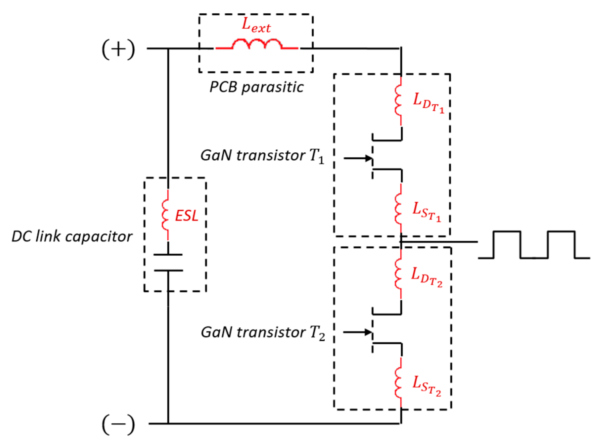
Figure 1. Parasitic inductances identification in the commutation loop on printed circuit board (PCB).
Energies 14 01495 g001
Figure 2. Characterization fixture (a) microstrip transmission line parameters (bottom layer as ground plane); (b) lateral commutation loop connected to transmission lines.
Energies 14 01495 g002
Figure 3. Organizational chart of the proposed modeling method.
Energies 14 01495 g003
Figure 4. SMA connector: (a) presentation of the connector; (b) proposed equivalent circuit.
Energies 14 01495 g004
Figure 5. Fixture 1 characterization and modeling: (a) experimental (photos) and simulation (circuit) setup; (b) measured vs. simulated inductance.
Energies 14 01495 g005
Figure 6. S-parameter measurement techniques: (a) 1-port reflection; (b) 2-port Shunt-Thru; (c) 2-port Series-Thru.
Energies 14 01495 g006
Figure 7. Series-Thru characterization: (a) measurement setup; (b) equivalent circuit.
Energies 14 01495 g007
Figure 8. Shunt-Thru characterization: (a) measurement setup; (b) equivalent circuit.
Energies 14 01495 g008
Figure 9. Lateral PCB loop: (a) test fixture; (b) simulation setup.
Energies 14 01495 g009
Figure 10. Lateral PCB loop inductance extraction: (a) measurement vs. simulation; (b) relative error.
Energies 14 01495 g010
Figure 11. Characterization of the drain–source inductance of a GaN transistor: (a) test fixture; (b) Cold FET equivalent circuit of the device.
Energies 14 01495 g011
Figure 12. Experimental determination of the drain–source inductance L D S T and electrical modeling.
Energies 14 01495 g012
Figure 13. Simulation of the GaN transistor drain–source inductance: (a) EM model with device PCB footprint; (b) EM model with device PCB footprint and added microstrip line.
Energies 14 01495 g013
Figure 14. Comparison between experimental drain–source inductance and EM modeling.
Energies 14 01495 g014
Figure 15. Schematic representation of the commutation loop characterization circuit.
Energies 14 01495 g015
Figure 16. Lateral commutation loop: (a) test fixture; (b) simulation setup.
Energies 14 01495 g016
Figure 17. Lateral commutation loop inductance extraction: (a) measurement vs. simulation; (b) relative error.
Energies 14 01495 g017
Figure 18. Vertical commutation loop configuration.
Energies 14 01495 g018
Figure 19. Vertical PCB loop: (a) test fixture; (b) simulation setup.
Energies 14 01495 g019
Figure 20. Vertical PCB loop inductance extraction: (a) measurement vs. simulation; (b) relative error.
Energies 14 01495 g020
Figure 21. Vertical commutation loop: (a) test fixture; (b) simulation setup.
Energies 14 01495 g021
Figure 22. Vertical commutation loop inductance extraction: (a) measurement vs. simulation; (b) relative error.
Energies 14 01495 g022
Figure 23. Switching waveforms measurement: (a) schematic representation of the test setup; (b) voltage waveforms of T 2 and load current.
Energies 14 01495 g023
Figure 24. Converters tests: (a) commutation cell with lateral loop; (b) commutation cell with vertical loop; (c) test setup with commutation cell, DC load and optically isolated voltage probes.
Energies 14 01495 g024
Figure 25. Experimental switching waveforms: (a) at turn-on of T 2 ; (b) at turn-off of T 2 .
Energies 14 01495 g025
Figure 26. Spectral analysis of GaN transistor T 2 V D S voltage for the two stuided commutation loops.
Energies 14 01495 g026
Table 1. Electromagnetic (EM) simulation setup for PCB design modeling.
S-Parameters ReferenceFrequency PlanMesh
Bottom layer (ground plane)1–2 GHz (adaptive)50 cells per wavelength
Table 2. Measured and simulated inductance values at 10 and 100 MHz for the different characterized loops.
10 MHz100 MHz
L l o o p l a t   ( nH ) L l o o p v e r   ( nH ) L l o o p v e r L l o o p l a t L l o o p l a t   ( nH ) L l o o p v e r   ( nH ) L l o o p v e r L l o o p l a t
Measurement12.354.850.3912.194.700.39
Simulation12.523.940.3212.363.800.31
Publisher’s Note: MDPI stays neutral with regard to jurisdictional claims in published maps and institutional affiliations.