Abstract
For medium voltage applications, multilevel inverters are used. One of its classic topologies is the Cascaded H-Bridge, which requires isolated DC voltages to work. Depending on the DC voltage ratio used in the Cascaded H-bridge can be classified into symmetric and asymmetric. In comparison between symmetric and asymmetric inverters, the latter can generate an AC output voltage with more output voltage levels. DC voltage ratio most documented are binary and trinary. The last can generate an AC voltage of 3n = 27 levels is obtained, using n = 3 inverters in cascade and NLM modulation, which generates a flow power of the load to the inverters (regeneration). This work analyzes the semiconductor losses (switching and conduction) and the THD of the AC output voltage in function of index modulation, considering a non-regenerative modulation technique for a 27-level single-phase asymmetric inverter. To confirm the theoretical analyzes, simulation and experimental results are shown.
1. Introduction
In applications for medium and high voltage drives, multilevel inverters are used [1,2]. By using low-voltage semiconductor devices, it is possible to generate any AC voltage [3]. The classic topologies within multilevel inverters are NPC [4], Clamped capacitor [5], and cascaded H-bridge (CHB) [6]. These topologies advantages are: (i) low distortion and low dv/dt AC voltage, (ii) low switching frequency, and (iii) low common-mode voltage [7].
Depending on the multilevel inverter’s topology, the number of power cells or semiconductors used to achieve the desired number of AC voltage levels can be a problem. An option to solve the problem indicated above is the use of CHB, with different DC voltages, which is called an asymmetric inverter [8]. Depending on the DC voltage ratio, this relationship can be binary [9] or tertiary [10], the latter being the most documented.
Some advantages of asymmetric inverters are: (i) generates an AC output voltage with low THD (<3%), when DC voltage ratio is tertiary, 1:3:9, with a reduced number of power cells and suitable modulation technique [10,11], (ii) minimize the switching frequency of semiconductors devices, and (iii) use effectively use the blocking characteristics of each device used in the power converter [12].
Despite these significant advantages, asymmetric inverters have the following disadvantages: (i) many isolated DC sources are required, this will depend on the number of output voltage levels [13], (ii) asymmetric power distribution, due to different DC voltages in the power cells [14], (iii) loss of modularity, due to its different values at their DC voltages [15], and (iv) depending on the DC voltage ratios, the existence of power flow between its power cells is possible, regardless of the type of load that the asymmetric inverter feeds, in specific when DC voltage ratio is trinary. The most traditional modulation technique used in trinary asymmetric inverters is (Nearest Level Modulation) NLM, but it generates the drawback indicated above. Thus, the use of this type of modulation in AC drives can be a problem, complicating the topology and/or its control [16,17,18,19].
Solutions to the last drawback above indicated are found in the literature as in [20], asymmetric inverters with 13 voltage levels have also been used [21], as well as the adequate DC voltage ratio [22], but in all cases, the THD of the AC output voltage is not optimal. On the other hand, a modulation technique with minimization of the output voltage THD has been developed for an asymmetric inverter with 15 levels [23], in the same way for an asymmetric inverter with 27 levels [24], both cases without flow of power from the load to the inverters.
A point that is not considered in this work is the economic one. However, the increase in the output voltage levels has a close relationship with reducing its harmonic content and low THD, but the economic cost is not considered to achieve these desired technical characteristics. The economic impact generated by the use and maintenance of a multilevel converter, in this case asymmetric, must be considered, in addition to its installation. Furthermore, when designing the converter, the number of components must be taken into account, such as: switches, drivers, heatsinks, voltage sensors, filters (if necessary) according to the converter’s power levels. A methodology for the above is explained in [25].
This work analyzes the 27-level single-phase asymmetric inverter without regeneration [24], Figure 1. It considers the quality of its output voltage waveform va(t) THD and its efficiency, evaluating the semiconductors losses before the variations of modulation index, variation of the DC voltage in the power cells, and variation of the power factor of the load that this inverter feeds. All of the above, in steady-state. Transient state analysis is not considered in this work because under this condition, the physical variables must have their limits both in value and time, such as blocking voltage, recovery current, dissipated power, collector current in the IGBT, and voltage and current in the load, etc. Furthermore, the modulation strategy analyzed considers the THD’s minimization in the voltage at the load, which is calculated for a steady-state waveform. To demonstrate the theoretical analyzes, simulation and experimental results will be shown.
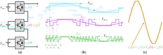
Figure 1.
(a) Topology single-phase Cascaded H-Bridge for asymmetric inverters with 27 levels with regeneration, (b) individual output voltage for m =1.0, (c) output voltage for m = 1.0.
The manuscript is organized as follows; Section 2 explained the methodology used to computed the efficiency in 27 Levels Single-Phase Asymmetric Inverter without Regeneration, the Section 3 shows the topology used in this study. Section 4 analyzes the switching frequency in the semiconductor devices, which depends on the modulation technique used in each power cell. Then, Section 5 presents the semiconductors losses. These losses are divided into two: (i) switching losses and (ii) conduction losses; both depend on the semiconductors devices parameters, the operating point of each power cell, and the modulation technique. In Section 6, simulated results are displayed for steady-state and disturbances, and in Section 7, experimental results are presented. Finally, in Section 8, the conclusions of the work are explained.
2. Methodology
To estimate efficiency, based on semiconductors losses, in the 27 Level Single-Phase Asymmetric Inverter without Regeneration, it is necessary to know specific parameters and operating conditions of the power converter.
The first is necessary to know the operating point of the power converter and the topology. In this case, these variables depend on the power cell, VDCi, IDCi, vai, (with i = 1, 2, 3), and others are common of the power cell, as load parameters (ZL, RL, LL, θ) and load current IL.
The second step is mandatory to know the parameters of the semiconductor. In this case, IGBT is used in all power cells because the VDC values are not high (experimental results with low power prototype). These parameters are used to characterize the IGBT turn-on, IGBT turn-off, and diode turn-off.
The third step is to analyze the modulation technique used in the power converter. In particular is interesting to obtain the switching frequency device in function of index modulation. In asymmetric inverters, this parameter depends on the power cell because the firing pattern is not the same between them.
The fourth step is to analyze the modulation technique but considering the load that feeds. Assuming that the asymmetric inverter feeds an AC motor, the simplified steady-state behavior is represented as RL load. Thus, the conduction time inside the semiconductor device depends on the θ of the load. When the voltage and current load has the same sign, IGBT is on, but the voltage and current do not have the same sign; the diode is on.
In the fifth step, the energy dissipated is estimated in the semiconductor devices considering [26], and finally the sixth step, the efficiency is computed.
The summary methodology is depicted in Figure 2.
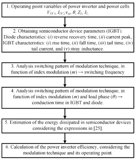
Figure 2.
Methodology used to compute efficiency in 27 levels single-phase asymmetric inverter without regeneration.
3. Topology
Figure 1a, is shown the topology used for the asymmetric inverter. It is based on CHB, in this case, by 3 H-bridge inverters connected in cascade. Using equal DC voltages, the AC output voltage has seven levels. An alternative is to use different DC voltage ratios to obtain a greater number of voltage levels at the output AC voltage.
Using a 1: 3: 9 trinary type DC voltage ratio, va(t) has 27 levels, obtaining a low THD. Commonly for this type of asymmetric inverter, the NLM modulation technique is used, which generates power flow between the power cells, Figure 3a, for specific values of the modulation index, regardless of the type of load it feeds [16,17,18,19]. The use of AFE rectifiers or dissipation resistors is necessary for specific applications, such as AC drives.
Figure 3.
Active power distribution. (a) 27-level single—phase asymmetric inverter with regeneration, (b) 27-level single—phase asymmetric inverter without regeneration.
An alternative is the use of an asymmetric inverter with a trinary DC voltage ratio, 1:3:9, where the calculation of the αi is done by minimizing the THD of the AC voltage, Figure 1b, considering as limitation that the voltages of each inverter vai,1, i = 1, 2, 3, are greater than or equal to zero. Avoiding the existence of regeneration [24], Figure 3b, but obtaining an output voltage with low THD (<3.0% for m = 1.0), Figure 1c. This solution eliminates the flow of power between the power cells, simplifying the converter’s topology and control.
4. Semiconductors Losses
4.1. Switching Losses
The switching process in semiconductor devices is not-ideal Figure 4, as shown in [27].
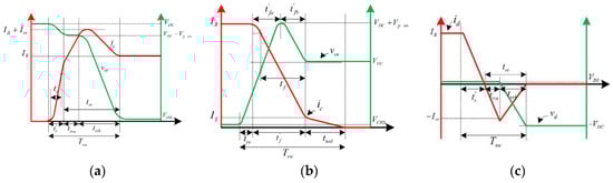
Figure 4.
Non-linear characteristic IGBT switching process. (a) IGBT Turn on, (b) IGBT Turn off, (c) Diode turn off.
In asymmetric inverters, the semiconductor device used in each power cell depends on the value of the DC voltage (blocking voltage) and the switching frequency, according to the switching pattern proposed by the modulation technique. Therefore, each power cell should have a different semiconductor device.
Due to the switches available for experimental results, only IGBTs are considered to analyze switching losses.
The losses in a switching period depend on the following factors: (i) the characteristics of the diode (reverse recovery time and current peak), (ii) characteristics of the IGBT (rise and fall time, tail time and tail current), and (iii) stray inductance. The diodes used in modern IGBTs are fast recovery diodes; thus, the losses due to switching on the diode are less than 1% compared to the losses due to switching off the diode [28]; they are neglected in the analysis. The loss estimation considers the IGBT switching on, the IGBT switching off, and the losses due to the diode switching off, as reviewed in [26].
4.2. Conduction Losses
In a semiconductor device, the conduction losses depend on the saturation voltage vsat, and the current flowing through it [29]. A first-order approximation is used to model the saturation voltage, considering threshold voltage VT, and series resistance RT, thus,
Then, the average power dissipated in the conduction of the semiconductors at the fundamental frequency is given by,
where IAVG corresponds to the average value of the current flowing through the semiconductor, and IRMS is the RMS value of the semiconductor current. Finally, the energy dissipated during a period is,
where TCOND is the conduction time of the semiconductor. In this work (3) is used to calculate conduction losses.
5. Switching Frequency
In each power cell of an asymmetric inverter, the output voltage is different, Figure 1b. This is to achieve full AC output voltage, with a high amount of levels and a low THD, Figure 1c. Due to this, the switching frequency of semiconductor devices is different for each power cell.
The switching frequency of a semiconductor device depends on the modulation index of the modulation technique. As the modulation index m decreases, the THD of the AC output voltage increases, Figure 5a. This is due to the disappearance of the firing angles αi; they tend to a 90°. Consequently, the inverter’s levels of the total output voltage are decreasing.
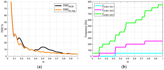
Figure 5.
(a) Comparison THD output voltage, comparison between NLM and no regenerative modulation technique [22] (b) Switching frequency distribution by semiconductor device.
The main inverter has a semiconductor device switching frequency (fswdev) of 50 Hz, until m = 0.33; in the remaining two secondary inverters (named in this way for the power supply to the load), their switching frequencies will depend on the pattern of firing of semiconductors and index modulation, Figure 6. For the secondary inverters of 27-level single-phase inverter without regeneration, the second inverter has fswdev = 250 Hz, and for the third inverter, fswdev = 850 Hz, the indicated values are for m = 1.0, where the switching frequency is maximum, and THD is minimum, Figure 5b. The gating pattern for m = 1.0 is shown in Figure 6a. As indicated aforementioned, when m decreases, the switching frequency changes in the semiconductor device, in Figure 6b shown the gating pattern for m = 0.7. Similarly, the gating signal activates the semiconductor device, in this case, IGBT with diode in antiparallel, but the activation of one of these two will depend on the voltage’s polarity the current in the load. If the polarity of the voltage and current load is the same, IGBT is on, otherwise the diode is turned on.
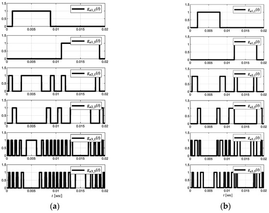
Figure 6.
Gate signals for semiconductors devices of 27-level single–phase asymmetric inverter with regeneration. (a) m = 1.0, (b) m =0.7.
6. Simulated Results
6.1. Steady-State Analysis
The asymmetric inverter of 27-level single-phase inverter without regeneration is analyzed, simulated in PSIM 2020a® [30]. The simulation’s schematic is shown in Figure 7, and the parameters are shown in Table 1, and the values of the αi used are presented in Table 2.
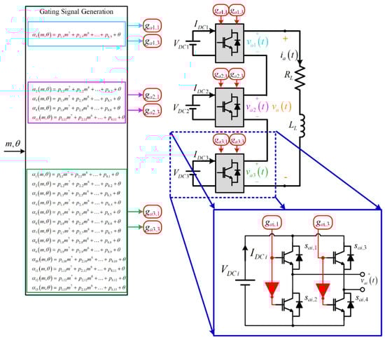
Figure 7.
Schematic of the simulation.

Table 1.
Simulated parameters.
Table 2.
Firing angles.
In Figure 8a is shown va(t). This voltage has 27 levels, with a THD of 3%. The load current is highly sinusoidal with a THD less than 1.0%. The spectrum harmonic of the load voltage is shown in Figure 8b, where the harmonics’ amplitude does not exceed 1.0%. Figure 8c shows the output voltage in each power cells vai(t); these are in phase allowing the harmonics generated by them to cancel each other, not appearing in the load voltage va(t); this condition is imposed by the THD minimization algorithm [24]. The above can be verified by Figure 8b,d.
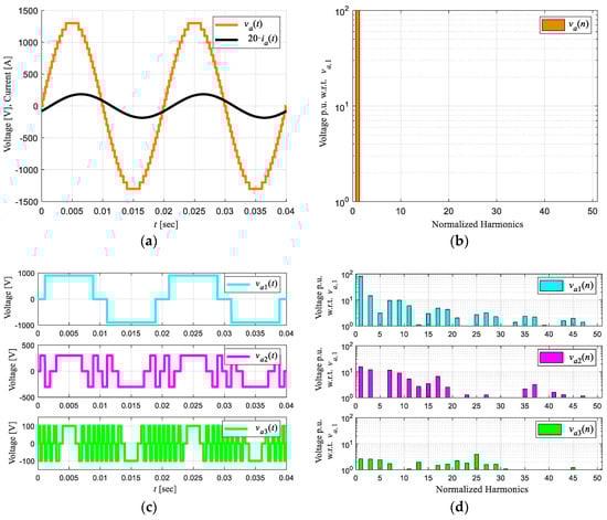
Figure 8.
Simulation results 27 levels single-phase asymmetric Inverter without regeneration for m = 1.0. (a) Output voltage and current, (b) Harmonic spectrum for output voltage va(t), (c) Individual inverter output voltages, (d) Harmonic spectrum va1(n), va2(n), and va3(n).
To check the modulation technique proposed in [24], it is simulated again for m = 0.7. The output voltage va(t) is shown, Figure 9a, which has 17 levels, a low harmonic content with a THD of 5.3% Figure 9b, and the load current is sinusoidal with a low THD of 1.3%. The NLM modulation technique presents current circulation between the inverters with lower DC link voltage [16,17,18,19], Figure 3a; this is because the phase between the voltage and the load current are 180° out of phase, even though the load is purely resistive. In the case of the analyzed technique [21], the inverter does not present current circulation between the inverters, Figure 9c; this agrees with what is shown in Figure 3b.
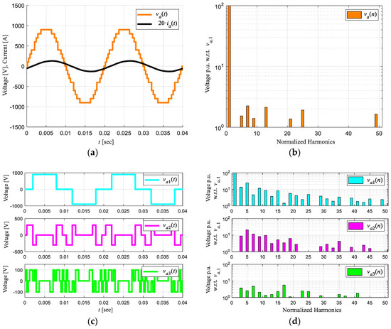
Figure 9.
Simulation results 27 levels single-phase asymmetric Inverter without regeneration for m = 0.7. (a) Output voltage and current, (b) Harmonic spectrum for output voltage va(t), (c) Individual inverter output voltages, (d) Harmonic spectrum va1(n), va2(n), and va3(n).
It can be appreciated, the value of the fundamental is zero for va2(n) and va3(n) for the value of m = 0.7, Figure 9d; this is imposed by the modulation technique proposed in [24]. With this, it is avoided that the asymmetric inverter’s secondary power cells have a power flow between them. Avoiding regeneration.
For the analysis of semiconductor losses, the IRG4BC20UDPBF IGBT switch [31] is considered. IGBTs are subjected to different dc voltages due to the voltage ratio used. This also determines the type of output voltage that they will generate, defining the switching frequency of the IGBTs.
The 27-level single-phase asymmetric inverter without regeneration has an efficiency of 96.22% for m = 1.0 and load power factor 0.8(i), with a THD of va(t) of 3%, considered the values shown in Table 1 and Table 2. The semiconductor losses distribution in Figure 10a is shown for the conditions listed above. It extends the previous analysis for the entire range of the modulation index 0.0 < m < 1.0, but the same load, Figure 10b. It is appreciated that the 27 levels single-phase asymmetric inverter without regeneration for a range 0.8 < m < 1.0, the output voltage has a THD < 5%, with an efficiency close to 96%.
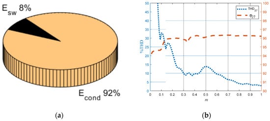
Figure 10.
(a) Semiconductor losses distribution for m = 1.0, (b) comparison between THDva and efficiency and 27 levels single—phase asymmetric inverter without regeneration, for all m.
6.2. Analysis before Disturbances
In an AC electrical system, voltage variations are allowed within a range of ±10%, where the equipment must be work. In applications such as AC drives, the DC voltage link can have a ripple; this depends on several factors, such as the power converter’s topology, the DC capacitor’s size, the type of load fed, and the operating point of the power converter [32].
Variations in AC voltage supply affect the DC voltage link in power cells. This dramatically affects the modulation technique analyzed in this work, not allowing the generation of the different output voltage levels, increasing its THD. We focus on analyzing how the DC voltage variation affects the efficiency of the 27 levels single-phase asymmetric inverter without regeneration.
As can be seen in Figure 11a, the DC voltage variation is ±10% [33], for a value of m that varies between 0.0 < m < 1.0. Despite the DC voltage variation in the power cells, the asymmetric inverter’s efficiency, for the same value of m, does not change more than 0.5%. This is because this variation mainly affects switching losses, which are not very significant regarding conduction losses for the modulation technique analyzed.
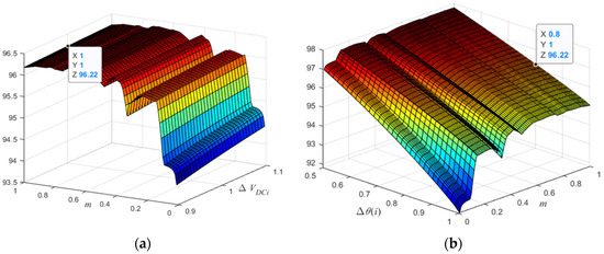
Figure 11.
Efficiency analysis in the event of disturbances. (a) VDCi variation v/s m, (b) θ(i) variation v/s m.
On the other hand, a variation of the load power factor that can supply this 27 levels single-phase asymmetric inverter without regeneration is analyzed for any value of m between 0.0 < m < 1.0, Figure 11b.
The lowest efficiency is when the inverter feeds a pure resistive load, the worst case is an efficiency of 91.81% and improves as the load has more inductive. This behavior is explained below.
Depending on the load power factor, there are instances of time where each power cell’s output voltage does not have the same polarity as the load current. This generates that the IGBT does not conduct for these moments, but rather its diode connected in antiparallel. According to the datasheet parameters, it consumes less energy in its conduction state than the IGBT [31].
Additionally, it should be considered that conduction losses are of greater importance for the modulation technique analyzed in this work, compared to switching losses.
7. Experimental Results
Finally, to verify what was theoretically exposed, a low-power experimental prototype was implemented. The schematic is very similar, shown in Figure 7. The parameters of the experimental results are shown in Table 3. The DSP TMS320C6713 is used to generate the firing pulses to activate the IRG4BC20UDPBF IGBT switch [31]. Unlike other jobs that use a look-up table. The authors use a polynomial approximation of the seventh degree to obtain the firing angles, which depends on the modulation index and the desired phase angle.
Table 3.
Experimental parameters.
Figure 12 is depicted the experimental results for m = 1.0. The output voltage va(t), has a THD of 3.45%, and the load current ia(t) is almost sinusoidal with a THD < 2%, Figure 12a. The voltage and current load is very similar to that shown in Figure 8a. The harmonic spectrum of va(t) is the depicted in Figure 12b, this has low-frequency harmonics, but amplitude is less than 2%. Compared with Figure 8b, it is slightly different due to the sampling time used, TS = 50 [µS]. With this TS, the amount of points for a period is 400, with a resolution of 0.9°, affecting the firing pulses for semiconductor devices. Then, the individual voltages vai(t) and load current ia(t) are depicted in Figure 12c; these are similar are shown in Figure 8c. As the asymmetric inverter feeds an RL load with a power factor of 0.8 (i), in some instances, the load current and individual voltages have not the same polarity; with this, the antiparallel diode in the IGBT is turned on. Thus, the diode’s forward voltage is significant concerning VDC2 and VDC3, Table 3, generating an offset DC in va2(t) and va3(t). Finally, Figure 12d shown the harmonic spectrum of the individual voltages vai(t); these are similar to the ones shown in Figure 8d.
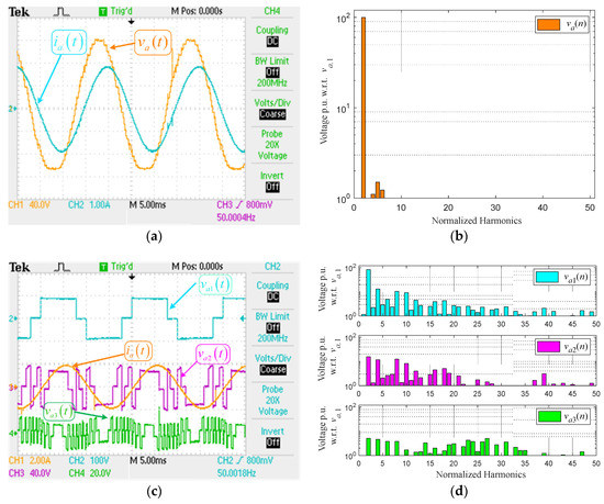
Figure 12.
Experimental key waveforms for m = 1.0. (a) output voltage va(t) and load current ia(t), (b) Harmonic spectrum for output voltage va(n), (c) Individual inverter output voltages vai(t) and load current ia(t), (d) Harmonic spectrum va1(n), va2(n), and va3(n).
The second test is for m = 0.7, where the NLM strategy presents regeneration for 27 levels asymmetric inverter, and the analyzed technique does not. Figure 13a shows the output voltage va(t) and load current ia(t), which is similar to the one shown in Figure 9a, va(t) has 17 levels and low harmonic content with a 6.5% THD. The harmonic spectrum of va(t) in Figure 13b, is similar at shown in Figure 9b. As mentioned above, the difference between the simulated and experimental results is due to the resolution of 0.9° by point. The individual voltages vai(t) and load current ia(t) are depicted in Figure 13c; the phase shift present between the voltage and current is due to the load power factor. In this case, the NLM approach presents a circulating current, creating regeneration in the lower DC voltage inverters. Figure 13d shows the experimental spectra of va1(n), va2(n) and va3(n), where the fundamental component of va2(n) and va3(n) is zero. On the other hand, the diode voltage drop in the IGBT is significant, due to the low DC voltages used in the experimental setup. Generating a slight displacement in va2(t) and va3(t). Despite the above, the modulation technique avoids power flow between the power cells with lower DC voltage.
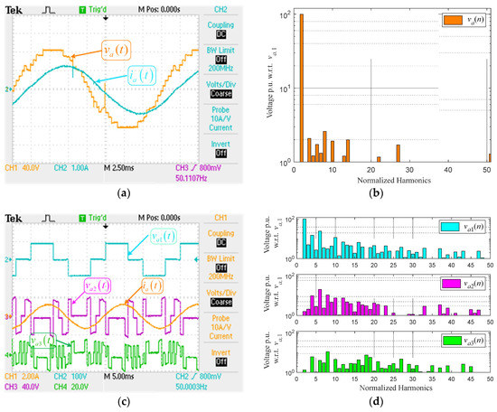
Figure 13.
Experimental key waveforms for m = 0.7. (a) output voltage va(t) and load current ia(t), (b) Harmonic spectrum for output voltage va(n), (c) Individual inverter output voltages vai(t) and load current ia(t), (d) Harmonic spectrum va1(n), va2(n), and va3(n).
8. Conclusions
An efficiency analysis has been performed to 27-level single-phase asymmetric inverter without regeneration, including THD of the output voltage. The analysis considers THD of the output voltage va(t) and the semiconductors losses as a function of the modulation index, DC voltage variation, and load power factor variation.
The 27 levels single-phase asymmetric inverter without regeneration for m = 1.0 and load power factor 0.8(i), has an efficiency η = 96.22%, with a THD of va(t) 3%. Considering a wider modulation index range, 0.8 < m < 1.0, the efficiency is near (η ≈ 96%) with a THD of va(t) < 5%. Furthermore, the analysis shows that when faced with variations in each power cell’s DC voltage, the efficiency does not changes much. The opposite case is with variations in the load power factor, where the efficiency can vary up to 5%, the worst case being an efficiency of 91.81% for m = 0.01.
With this background, the 27-level single-phase asymmetric inverter, with a modulation technique that prevents the flow of power between its power cells, is a good alternative for low and medium voltage applications, thanks to its high efficiency and output voltage with high quality.
Author Contributions
Formal analysis, E.E.; Funding acquisition, E.E.; Methodology, P.M. and C.B.; Software, C.B. and H.G.; Supervision, J.E.; Writing—original draft, E.E.; Writing—review & editing, P.M., J.E. and H.G. All authors have read and agreed to the published version of the manuscript.
Funding
E.E., P.M., C.B., J.E., and H.G. would like to express their gratitude to Universidad Católica de la Santísima Concepción, Dirección de Investigación, for its immense support under Grant DIN 12/2016.
Institutional Review Board Statement
Not applicable.
Informed Consent Statement
Not applicable.
Data Availability Statement
Data available on request due to restrictions privacy. The data presented in this study are available on request from the corresponding author.
Acknowledgments
The authors would like to acknowledge the financial support received from Universidad Católica de la Santísima Concepción, Dirección de Investigación, through Grant DIN 12/2016 and ANID/FONDAP SERC/15110019.
Conflicts of Interest
The authors declare no conflict of interest.
References
- Akagi, H. Multilevel Converters: Fundamental Circuits and Systems. Proc. IEEE 2017, 105, 2048–2065. [Google Scholar] [CrossRef]
- Wu, B.; Narimani, M. Voltage Source Inverter Fed Drives. In High-Power Converters and AC Drives, 2nd ed.; Wiley-IEEE Press: Piscataway, NJ, USA, 2017; pp. 287–308. [Google Scholar]
- Leon, J.I.; Vazquez, S.; Franquelo, L.G. Multilevel Converters: Control and Modulation Techniques for Their Operation and Industrial Applications. Proc. IEEE 2017, 105, 2066–2081. [Google Scholar] [CrossRef]
- Nabae, A.; Takahashi, I.; Akagi, H. A new Neutral-Point-Clamped PWM Inverter. IEEE Trans. Ind. Appl. 1981, 1A-17, 518–523. [Google Scholar] [CrossRef]
- Lai, J.S.; Peng, F.Z. Multilevel converters-A new breed of power converters. IEEE Trans. Ind. Appl. 1996, 32, 509–517. [Google Scholar]
- Hammond, P. A new approach to enhance power quality for medium voltage AC drives. IEEE Trans. Ind. Appl. 1997, 33, 202–208. [Google Scholar] [CrossRef]
- Abu-Rub, H.; Bayhan, S.; Moinoddin, S.; Malinowski, M.; Guzinski, J. Medium-Voltage Drives: Challenges and existing technology. IEEE Power Electron. Mag. 2016, 3, 29–41. [Google Scholar] [CrossRef]
- Mueller, O.M.; Park, J.N. Quasi-linear IGBT inverter topologies. In Proceedings of the IEEE Applied Power Electronics Conference and Exposition—ASPEC’94, Orlando, FL, USA, 13–17 February 1994; IEEE: Piscataway, NJ, USA, 1994; pp. 253–259. [Google Scholar]
- Vasu, R.; Chattopadhyay, S.K.; Chakraborty, C. Asymmetric Cascaded H-Bridge Multilevel Inverter with Single DC Source per Phase. IEEE Trans. Ind. Electron. 2020, 67, 5398–5409. [Google Scholar] [CrossRef]
- Manoharan, M.S.; Ahmed, A.; Park, J.-H. An Improved Model Predictive Controller for 27-Level Asymmetric Cascaded Inverter Applicable in High-Power PV Grid-Connected Systems. IEEE J. Emerg. Sel. Top. Power Electron. 2020, 8, 4395–4405. [Google Scholar] [CrossRef]
- Manoharan, M.S.; Ahmed, A.; Park, J. A PV Power Conditioning System Using Nonregenerative Single-Sourced Trinary Asymmetric Multilevel Inverter with Hybrid Control Scheme and Reduced Leakage Current. IEEE Trans. Power Electron. 2017, 32, 7602–7614. [Google Scholar] [CrossRef]
- Perez, R.J.; Beristain, J.J.A.; Hernández, L.J.H.; Urquijo, R.F.R. Hybrid Modulation Strategy for Asymmetrical Cascade H-Bridge Multilevel Inverters. IEEE Lat. Am. Trans. 2018, 16, 1623–1630. [Google Scholar]
- Ahmed, A.; Manoharan, M.S.; Park, J. An Efficient Single-Sourced Asymmetrical Cascaded Multilevel Inverter with Reduced Leakage Current Suitable for Single-Stage PV Systems. IEEE Trans. Energy Convers. 2019, 34, 211–220. [Google Scholar] [CrossRef]
- Perez, M.; Rodriguez, J.; Pontt, J.; Kouro, S. Power Distribution in Hybrid Multi-cell Converter with Nearest Level Modulation. In Proceedings of the IEEE International Symposium on Industrial Electronics, Vigo, Spain, 4–7 June 2007; IEEE: Piscataway, NJ, USA, 2007; pp. 736–741. [Google Scholar]
- Busarello, T.D.C.; Reuter, A.L.d.M.; Péres, A.; Simões, M.G. Understanding the Staircase Modulation Strategy and Its Application in Both Isolated and Grid-Connected Asymmetric Cascaded H-Bridge Multilevel Inverters. IEEE Trans. Ind. Appl. 2019, 55, 5371–5382. [Google Scholar] [CrossRef]
- Flores, P.; Dixon, J.; Ortuzar, M.; Carmi, R.; Barriuso, P.; Moran, L. Static Var Compensator and Active Power Filter With Power Injection Capability, Using 27-Level Inverters and Photovoltaic Cells. IEEE Trans. Ind. Electron. 2009, 56, 130–138. [Google Scholar] [CrossRef]
- Dixon, J.; Pereda, J.; Castillo, C.; Bosch, S. Asymmetrical Multilevel Inverter for Traction Drives Using Only One DC Supply. IEEE Trans. Veh. Tech. 2010, 59, 3736–3743. [Google Scholar] [CrossRef]
- Dixon, J.; Breton, A.A.; Rios, F.E.; Rodriguez, J.; Pontt, J.; Perez, M.A. High-Power Machine Drive, Using Nonredundant 27-Level Inverters and Active Front End Rectifiers. IEEE Trans. Power Electron. 2007, 22, 2527–2533. [Google Scholar] [CrossRef]
- Pereda, J.; Dixon, J. High-Frequency Link: A Solution for Using Only One DC Source in Asymmetric Cascaded Multilevel Inverters. IEEE Trans. Ind. Electro. 2011, 58, 3884–3892. [Google Scholar] [CrossRef]
- Rotella, M.; Peñailillo, G.; Pereda, J.; Dixon, J. PWM Method to Eliminate Power Sources in a Nonredundant 27-Level Inverter for Machine Drive Applications. IEEE Trans. Ind. Electron. 2009, 56, 194–201. [Google Scholar] [CrossRef]
- Espinosa, E.; Espinoza, J.R.; Melin, P.; Ramírez, R.; Villarroel, F.; Muñoz, J.; Moran, L. A New Modulation Method for a 13-Level Asymmetric Inverter towards Minimum THD. IEEE Trans. Ind. Appl. 2014, 50, 1924–1933. [Google Scholar] [CrossRef]
- Lu, S.; Mariéthoz, S.; Corzine, K.A. Asymmetrical Cascade Multilevel Converters with Noninteger or Dynamically Changing DC Voltage Ratios: Concepts and Modulation Techniques. IEEE Trans. Ind. Electron. 2010, 57, 2411–2418. [Google Scholar]
- Espinosa, E.; Espinoza, J.; Ramirez, R.; Rohten, J.; Villarroel, F.; Melin, P.; Guzman, J. A new modulation technique for 15-level asymmetric inverter operating with minimum THD. In Proceedings of the IECON 2013—39th Annual Conference of the IEEE Industrial Electronics Society, Vienna, Austria, 10–13 November 2013; IEEE: Piscataway, NJ, USA, 2013; pp. 6164–6169. [Google Scholar]
- Espinosa, E.; Espinoza, J.; Villarroel, F.; Muñoz, J.; Melin, P.; Ramirez, R. A novel modulation technique for asymmetric multi-cell inverters of 27-level without regeneration. In Proceedings of the IECON 2012—38th Annual Conference on IEEE Industrial Electronics Society, Montreal, QC, Canada, 25–28 October 2012; IEEE: Piscataway, NJ, USA, 2012; pp. 123–128. [Google Scholar]
- Saif, A.M.; Buccella, C.; Patel, V.; Tinari, M.; Cecati, C. Design and Cost Analysis for STATCOM in Low and Medium Voltage Systems. In Proceedings of the IECON 2018—44th Annual Conference of the IEEE Industrial Electronics Society, Washington, DC, USA, 21–23 October 2018; IEEE: Piscataway, NJ, USA, 2018; pp. 3938–3943. [Google Scholar]
- Espinosa, E.; Espinoza, J.; Rohten, J.; Ramirez, R.; Reyes, M.; Muñoz, J.; Melin, P. An efficiency comparison between a 18 pulses diode rectifier and a multi-cell AFE rectifier operating with FCS—MPC. In Proceedings of the IECON 2014—40th Annual Conference of the IEEE Industrial Electronics Society, Dallas, TX, USA, 29 October–1 November 2014; IEEE: Piscataway, NJ, USA, 2014; pp. 1214–1220. [Google Scholar]
- Rajapakse, A.D.; Gole, A.M.; Wilson, P.L. Electromagnetic transients simulation models for accurate representation of switching losses and thermal performance in power electronic systems. IEEE Trans. Power Deliv. 2005, 20, 319–327. [Google Scholar]
- Schonberger, J.; Feix, G. Modelling turn-off losses in power diodes. In Proceedings of the 11th Workshop on Control and Modeling for Power Electronics, Zurich, Switzerland, 17–20 August 2008; IEEE: Piscataway, NJ, USA, 2008; pp. 1–6. [Google Scholar]
- Wiechmann, E.P.; Aqueveque, P.; Burgos, R.; Rodriguez, J. On the Efficiency of Voltage Source and Current Source Inverters for High-Power Drives. IEEE Trans. Ind. Electron. 2008, 55, 1771–1782. [Google Scholar] [CrossRef]
- Power Electronics SOFTWARE Simulation PSIM 2020A. Available online: https://powersimtech.com/ (accessed on 16 February 2021).
- Datasheet IRG4BC20UDPbF. Insulated Gate Bipolar Transistor with Ultrafast Soft Recovery Diode, International Rectifier. Available online: http://www.irf.com/product-info/datasheets/data/irg4bc20udpbf.pdf (accessed on 16 February 2021).
- Kuoro, S.; Lezana, P.; Angulo, M.; Rodriguez, J. Multicarrier PWM with DC-Link Ripple Feedforward Compensation for Multilevel Inverters. IEEE Trans. Power Electron. 2008, 23, 52–59. [Google Scholar] [CrossRef]
- Sarmiento, H.G.; Estrada, E. A Voltage Sag Study in an Industry with Adjustable Speed Drives. IEEE Ind. Magaz. Appl. 1996, 2, 16–19. [Google Scholar] [CrossRef]
Publisher’s Note: MDPI stays neutral with regard to jurisdictional claims in published maps and institutional affiliations. |
© 2021 by the authors. Licensee MDPI, Basel, Switzerland. This article is an open access article distributed under the terms and conditions of the Creative Commons Attribution (CC BY) license (http://creativecommons.org/licenses/by/4.0/).