Article

Tin Oxide Modified Titanium Dioxide as Electron Transport Layer in Formamidinium-Rich Perovskite Solar Cells

1
Department of Mechanical Engineering, Worcester Polytechnic Institute, 100 Institute Road, Worcester, MA 01609, USA
2
Department of Materials Science and Engineering, African University of Science and Technology, Km. 10 Airport Road, Abuja 900107, Nigeria
3
Department of Mathematics, Physics and Computing, Moi University, P.O. Box 3900-30100, Eldoret 3 0107, Kenya
4
Program in Materials Science and Engineering, Department of Mechanical Engineering, Worcester Polytechnic Institute, 100 Institute Road, Worcester, MA 01609, USA
5
Department of Theoretical and Applied Physics, African University of Science and Technology, Km. 10 Airport Road, Abuja 900107, Nigeria
6
CEMHTI-CNRS Site Cyclotron, 3A Rue de la Férollerie, 45071 Orléans, France
7
Department of Biomedical Engineering, Worcester Polytechnic Institute, 60 Prescott Street, Gateway Park Life Sciences and Bioengineering Center, Worcester, MA 01609, USA
*
Author to whom correspondence should be addressed.
Energies 2021, 14(23), 7870; https://doi.org/10.3390/en14237870
Submission received: 25 September 2021 / Revised: 18 October 2021 / Accepted: 2 November 2021 / Published: 24 November 2021
(This article belongs to the Topic Solar Thermal Energy and Photovoltaic Systems)

Abstract

:
The design of electron transport layers (ETLs) with good optoelectronic properties is one of the keys to the improvement of the power conversion efficiencies (PCEs) and stability of perovskite solar cells (PSCs). Titanium dioxide (TiO2), one of the most widely used ETL in PSCs, is characterized by low electrical conductivity that increases the series resistance of PSCs, thus limiting their PCEs. In this work, we incorporated tin oxide (SnO2) into titanium dioxide (TiO2) and studied the evolution of its microstructural and optoelectronic properties with SnO2 loading. The thin films were then integrated as ETLs in a regular planar Formamidinium (FA)-rich mixed lead halide PSCs so as to assess the overall effect of SnO2 incorporation on their charge transport and Photovoltaic (PV) characteristics. Analysis of the fabricated PSCs devices revealed that the best performing devices; based on the ETL modified with 0.2 proportion of SnO2; had an average PCE of 17.35 ± 1.39%, which was about 7.16% higher than those with pristine TiO2 as ETL. The improvement in the PCE of the PSC devices with 0.2 SnO2 content in the ETL was attributed to the improved electron extraction and transport ability as revealed by the Time Resolved Photoluminescence (TRPL) and Electrochemical Impedance Spectroscopy (EIS) studies.

1. Introduction

Perovskite solar cells (PSCs) have emerged as one of the low-cost photovoltaic (PV) technologies with photoconversion efficiencies comparable to those of the conventional crystalline silicon based solar cells [1,2]. They consist of photoactive perovskite layers that are sandwiched between two oppositely doped charge transport layers (CTLs) to form regular (n-i-p) or inverted (p-i-n) device architectures with electrodes on either side [3,4]. Within these architectures, the perovskite layer absorbs light and generates charge carriers that are injected into the CTLs before being transported in opposite directions to their respective electrodes where they are collected as electric current [5].
The charge carrier collection efficiency and hence the overall power conversion efficiency (PCE) of PSCs depends on the effectiveness of light absorption [6] and the accompanying charge carrier dynamics [7] that occur within the PSC structure. Owing to the exceptional optoelectronic properties of the perovskite active layer such as high light absorption ability [6], low exciton binding energies [8], balanced ambipolar charge carrier transport [7,9], high defect tolerance and long carrier diffusion lengths [10], the charge carriers in the Active Layer (AL) are effectively generated, separated and transported to the interface with CTLs when PSCs are illuminated [11].
One of the main hindrances to achieving high PCEs in PSCs is the low charge carrier collection efficiency that is associated with non-radiative recombination losses arising from inadequate extraction and transportation of photo-generated charge carriers through the CTLs to the electrodes [12,13,14,15]. These processes are mainly governed by the material properties of the CTLs and the nature of the interface they form with the AL [16,17]. In order to further improve the performance of PSCs, the CTLs ought to be designed to achieve a good optical transparency, excellent carrier selectivity, good electrical conductivity and band energy levels that align well with those of the AL [18,19].
In planar PSCs with n-i-p configurations, the ETL not only plays a key role in the extraction and transportation of photo-generated electrons [20] but also in the light absorption and the crystallization dynamics of the AL [21]. Hence, different materials have been explored for use as ETLs in PSCs with those based on metal oxide semiconductors; either in mesoporous and/or compact forms, proving to be attractive in terms of PCE and stability [19,22,23,24]. Among the metal oxide semiconductors, titanium dioxide (TiO2) is the most commonly used ETL due to its high transmittance in the visible light regime, low cost, good chemical stability, non-toxicity and the ease with which its properties can be tuned with minimal impact on its structure [25,26]. However, TiO2 has low electrical conductivity that increases the series resistance (Rs) and cause power losses in PSCs [27,28].
Modification of TiO2 through strategies such as doping with cations/anions [29], hybridization with graphene derivatives [30,31], forming core-shell nanostructures [32] and coupling with other n-type semiconductors [33,34] is an effective method to improve its optoelectronic properties which consequently leads to an improvement in the PCEs and stability of PSCs [35]. Tin (IV) Oxide (SnO2) is one of the n-type metal oxide semiconductors that has successfully been used to tune the optoelectronic properties of TiO2 for applications in photocatalysis [34], gas sensing [36] and in dye-sensitized solar cells [37,38]. It has a similar crystal structure with TiO2 but exhibits higher optical transmittance, higher electrical conductivity, better UV stability and is more favorable for the growth of perovskite films than TiO2 [20,39].
The synergetic effects that arise from the combination of SnO2 and TiO2 to form either a bi-layered or composite ETL structure have been utilized to improve the PCE and stability of PSCs [40,41,42,43,44,45,46]. The improvement has mainly been attributed to suppression of charge carrier recombination and accelerated extraction of the photo-generated electrons resulting from better energy level alignment and defect passivation at the ETL/perovskite interface [46]. Though the few studies that have been done on the use of SnO2-TiO2 nano-composite as ETLs in PSCs have shown that they help to improve the performance [40,47,48], the underlying physical and intrinsic phenomena that are responsible for the reported improvement are not clear, necessitating the need for more research in this area. In particular, the evolution of the properties of TiO2 with SnO2 loading, its possible impacts on the optoelectronic properties of the perovskite film and how it influences the overall charge transport kinetics and performance metrics of PSC requires further investigation.
This paper presents the results of the effects of SnO2 incorporation in TiO2-based ETL on the charge carrier dynamics and performance characteristics of planar Formamidium (FA)-rich mixed lead halide PSCs. First, we processed the ETL thin films on Fluorine doped Tin oxide (FTO)-coated glass substrates and studied the evolution of their structural, morphological, and optoelectronic properties with the proportion of SnO2 in TiO2. We then fabricated a series of planar regular PSCs that incorporated the SnO2-TiO2 and pristine TiO2 thin films as ETLs and compared their performance parameters. The results are then discussed for the design of efficient PSCs.

2. Materials and Methods

2.1. Materials

Unless otherwise stated, all the materials and reagents used in this work were purchased from Sigma Aldrich and used in the as-received condition. They include Titanium diisopropoxide, Tin (IV) Oxide nanoparticles (2.5% weight in butanol, nanoparticle size < 20 nm), Formamidinium iodide (FAI), Methylammonium Chloride (MACl), Methylammonium Bromide (MABr), Lead (II) Iodide, Spiro-OMeTAD and Fullerene C60. Dimethyl sulfoxide (DMSO), anhydrous N,N-dimethylformamide (DMF), Chlorobenzene were among the solvents used. Gold pellets (99.999%) were purchased from Kurt J. Lesker Company. 1925 Route 51, Jefferson Hills, PA 15025, USA.

2.2. Processing of ETL Thin Films

FTO-coated glass substrates were patterned using zinc powder and 2M Hydrochloric acid and cleaned sequentially in an ultrasonic bath using detergent, deionized water, acetone and isopropyl alcohol (IPA) for 15 min each. The substrates were then blow-dried using nitrogen gas before being treated with UV ozone for 15 min in order to remove any residual organic matter. Solutions of 0.15 M and 0.3 M of compact TiO2 were then prepared by dissolving 55 µL and 110 µL of titanium diisopropoxide bis(acetylacetonate) respectively in 1ml of 1-butanol. SnO2 nano-particle ink (2.5% in butanol, particle size < 20 nm) was then incorporated into the 0.15 M and 0.3 M TiO2 solutions in different volume fractions of 0.1, 0.2 and 0.3 to obtain SnO2-TiO2 mixed solutions. The mixed solutions were sonicated for 30 min before being spin-coated onto the FTO-coated glass substrates. The solutions containing 0.15 M were first spin-coated onto the FTO coated glass at 2000 rpm for 30 s, annealed at 150 °C for 5 min and allowed to cool to room temperature. This was followed by spin-coating of the mixed solution containing 0.3M TiO2 at 2000 rpm for 30 s before sintering at 500 °C for 30 min on a hot plate under ambient conditions. The thin film of pristine TiO2 was also prepared following the same protocol. Figure 1a–f presents the schematics of the processing procedure of the ETL thin films.

2.3. Fabrication of PSCs

Planar PSCs were prepared based on the modified and pristine TiO2 as ETLs via a spin-coating technique. First, the ETLs were prepared on cleaned FTO-coated glass substrate as per the procedure summarized in Figure 1a–f. Perovskite films were then deposited on the ETLs via a two-step spin-coating process described elsewhere [49]. The films were annealed at 130 °C for 15 min before the Spiro-OMeTAD solution was spin-coated onto it at 4000 rpm for 30 s. A thin layer of gold (80 nm) was deposited on the Spiro-OMeTAD film to form an electrode using a thermal evaporator (Edward E306A, UK).

2.4. Characterization of Materials

The morphological, structural, optical, and electrical properties of the ETL thin films were investigated using various characterization techniques. The microstructural images of the films and elemental composition were obtained using a field emission scanning electron microscope (SEM) (JEOL JSM-700F, Hollingsworth & Vose, MA, USA) that was instrumented with an energy dispersive X-ray spectrometer (EDS) (Oxford Instrument). The X-ray diffraction (XRD) patterns of the films were obtained using an X-ray diffractometer (Malvern PANalytical, Westborough, MA, USA) under Cu Kα radiation source at a voltage of 40 kV, current of 40 mA. This was done with a scanning step size of 0.01° and 2θ angles in the range of 20–90°. The optical properties of the thin films were measured using an Ultraviolet-Visible (UV-Vis) spectrometer (AVANTES Starline, Avaspec-2048) in the wavelength range of 200 nm to 1100 nm.
The current density-voltage (J-V) characteristics of the films and PSC devices were studied using Keithley 2400 source meter unit (Keithley, Tektronix, Newark, NJ, USA) interfaced with a computer. In the case of PSC devices, the Keithley system was connected to an Oriel solar simulator (Oriel, Newport Corporation, Irvine, CA, USA) and the J-V curves were obtained under AM1.5G illumination of 100 mW/cm2. The J-V measurement for the PSC device was carried out on a device area of 0.1 cm2 with a voltage scan range of −0.4 to 1.2 V. The electrochemical impedance spectroscopy (EIS) of the fabricated PSCs were measured under illumination using a potentiostat (SP-300, BioLogic Instrument). The impedance measurements were performed at a bias voltage of 0.1 V with an AC signal of amplitude 10mV in the frequency range 1 MHz to 1 Hz while the external quantum efficiency measurement was carried out with Quantx-300 quantum efficiency measurement system.

3. Results and Discussion

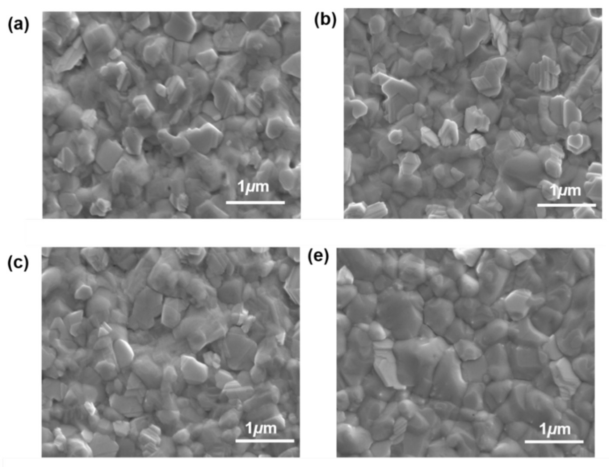
3.1. Structure and Morphology of the ETL and Perovskite Thin Films

The microstructural characteristics of the ETL and perovskite films play an important role in the charge carrier dynamics and the overall performance of PSCs. Compact morphologies with less pinholes and grain boundaries are essentially needed to form good interfacial contacts with adjacent layers and to reduce power losses due to series resistance, current leakage and charge carrier trapping [50]. The SEM images of the ETL thin films with different proportions of SnO2 are presented in Figure 2a–d. As seen in the figure, the SEM images of the ETLs with 0, 0.1 and 0.2 proportions of SnO2 (Figure 2a–c) are smooth and more compact when compared to the one with 0.3 proportion of SnO2 which appears to be porous and with more pinholes (Figure 2d). The formation of pinholes at higher SnO2 content can be associated with agglomeration of SnO2 nanoparticles or the degradation of SnO2 at higher annealing temperature [51]. The presence of the pinholes in these films can provide shunting paths that cause current leakage from the active layer to the FTO thus reducing the fill factor (FF) and the overall PCEs of PSC devices.
The elemental composition of the ETLs was studied by taking the EDS cross-sectional images. Figure 3a,b shows the SEM and EDS cross-sectional images of the representative SnO2-TiO2 ETL film deposited on FTO-coated glass substrate. From the figure, a thin layer of the ETL (around 100 nm in thickness) is visible on top of the FTO with an even distribution of Sn (Green) and Ti (Red). The EDS spectra of the ETLs at different SnO2 content are presented in Figure S1 in the Supplementary Materials. From the figure, we see that Sn, Ti and O are present in all the ETL films with different weight percentages. The SnO2-TiO2 based ETLs showed a higher Sn content relative to the TiO2-based ETL and the percentage weight of Sn increased with the SnO2 content. This confirms successful incorporation of SnO2 in TiO2. The Sn signals detected in the pristine TiO2 ETL possibly diffused from the underlying FTO layer during the sintering process. The other elements detected such as Si, Mg, and Cu, originated from glass substrate and the copper tape that was used to attach the samples to the sample holder while Pd and Au came from the coating film used.
To investigate the possible impact of SnO2 incorporation on the structural properties of the ETL films, the XRD patterns of the different films were recorded at room temperature (25 °C). Figure 3c shows the XRD patterns of all the ETL films at different proportions of SnO2. The result shows that the diffraction peaks of all the ETL films occur at 2θ angles of 26.5°, 33.8°, 37.8°, 51.8°, 61.6° and 66° which can respectively be indexed to the planes (110), (011), (020), (121), (130) and (031) for tetragonal titanium tin oxide composite (ICSD 98-009-0868). The (020) plane is the preferred crystal orientation in nearly all the ETL films except the one containing 0.2 SnO2 proportion whose preferred crystal orientation is the plane (110). Another observable difference in the diffractograms of the ETL films lies on the intensity of the diffraction peaks. The intensity of the peak corresponding to the plane (011) (labelled #) is observed to increase with the content of SnO2 in the ETL and reaches the highest value at SnO2 proportion of 0.2. The fullwidth at half maximum (FWHM) of the peak was also found to decrease with increasing SnO2 content attaining a minimum value at the same SnO2 proportion (Figure 3d). This shows that the ETL film with 0.2 proportion of SnO2 had better crystallinity relative to the rest.
In regular planar PSCs, the ETL forms the base over which the perovskite layer is deposited. This means that any variation in its surface characteristics can influence the crystallization dynamics and morphology of the perovskite films. We studied the effect of the ETL modification on the morphological properties of the perovskite films deposited on them by taking the SEM images of the top surface. The SEM images of the perovskite films formed on pristine TiO2 and SnO2-TiO2 based ETLs are presented in Figure 4a–d. From the figure, we observe a slight change in the morphology for the perovskite films deposited on the ETL containing 0.3 volume proportion of SnO2. At this proportion, the perovskite film appears to have larger interconnected grains with less grain boundaries when compared to rest. This implies that higher SnO2 content in the ETL resulted in the growth of perovskite films with improved morphologies. This observation is in agreement with what has been reported by other researchers [20].

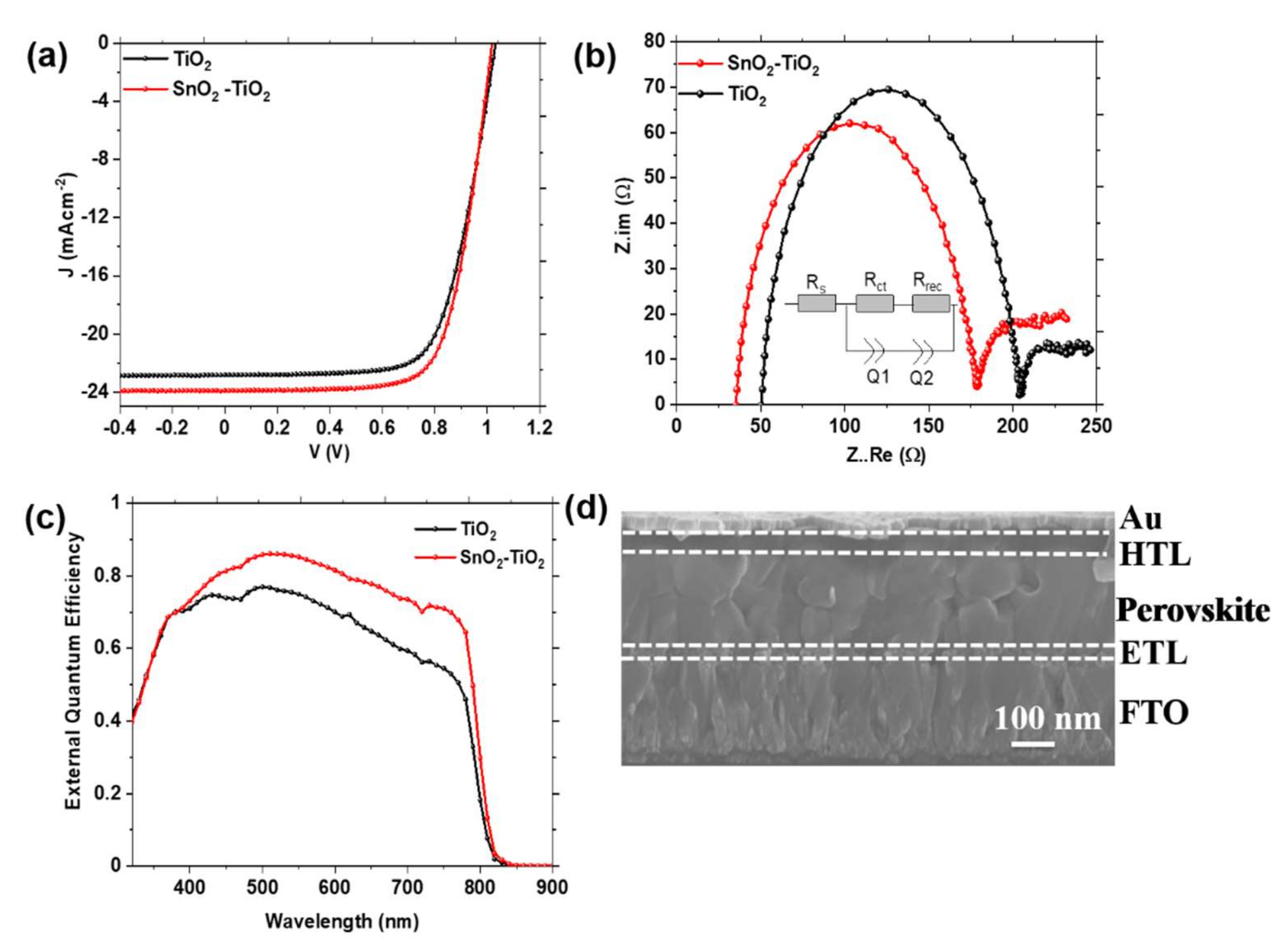
3.2. Optoelectronic Properties of the Thin Films

The optical properties of the ETL in PSCs can influence the amount of light reaching the photoactive perovskite layer, thus affecting the charge carrier generation. We studied the effect of SnO2 incorporation on the optical properties of the ETL films by measuring their transmittance and absorbance at different proportions of SnO2. The transmittance and absorption spectra of the different ETL films were measured in the range of 200 nm to 1100 nm using UV-Vis spectrometer. The optical transmittance spectra (Figure 5a) indicate that all the ETL films had high transmittance within the visible spectrum which makes them suitable for PV application. The ETL films modified with 0.2 and 0.3 SnO2 proportion exhibited higher transmittance relative to TiO2. The optical band gaps (Eg) of the ETL films at different proportions of SnO2 were determined from absorbance by plotting α h v verses the photon energy h ν and fitting the linear section of the resulting curve to the Tauc relation given in Equation (1) [52,53].
α h v 1 γ = B h ν E g
In Equation (1), α is the absorption coefficient of the ETL films, B is the edge width parameter and γ is a parameter that specifies the nature of the optical transition and usually takes a value of 2 for indirect optical transitions [53]. As shown in Figure 5b, we see a general blue-shift in the band gaps of ETL films as the SnO2 content increases. The band gap increased from 3.58 eV to 3.70 eV when the volume proportion of SnO2 increased from 0 to 0.3. The increase in band gap explains the observed increase in transmittance of the ETL films with the content of SnO2 in TiO2.
The electrical properties of the ETL films are also very important as they influence their electron transport function in PSCs. Good electrical conductivity ensures proper extraction of the photogenerated electrons and reduces the series resistance (Rs) of PSC devices. We determined the electrical conductivity (σ) of the ETL films at room temperature from the Ohmic region of their dark I-V curves (Figure 5c) which were obtained by applying voltage to the films sandwiched between two electrodes (FTO/ETLs/Au). The results show that σ increases with the SnO2 content in TiO2 and the highest value was obtained for the film modified with 0.2 volume proportion of SnO2. Beyond the 0.2 proportion of SnO2, the value of σ was found to decrease slightly (Figure 5d). The decrease in σ is attributed to the microstructural changes of the ETL at 0.3 proportion of SnO2 revealed by the SEM image in Figure 2d. The evolution of the bandgap and σ with SnO2 content in the ETL are summarized in Table S1 of the Supplementary Materials.
To understand the effect of ETL modification on the electron transport dynamics of the PSCs, we investigated the variation of the optoelectronic properties of perovskite films deposited on pristine TiO2 and SnO2-TiO2 ETLs through UV-Vis, steady state photoluminescence (PL), time resolved photoluminescence (TRPL) and space charge limited conduction (SCLC) techniques. The UV-Vis spectra of the perovskite films (Figure 6a) show that all the films had nearly equal absorption onsets (~800 nm) with a slight variation in their absorption intensities. This shows that the different proportions of SnO2 in the ETL layer did not cause alter the band gap of the perovskite films. The PL spectra of the perovskite films (Figure 6b) also show one major peak, all centered at ~800 nm, with small variations being observed only in their emission intensities. In particular, the PL emission peak for the perovskite film deposited on TiO2 modified with 0.3 volume proportion of SnO2 is stronger than those of the perovskite films deposited on pristine TiO2, and composite SnO2-TiO2 ETL with 0.1 and 0.2 SnO2 contents. This change in the PL intensity of perovskite film is usually associated with the variation in the crystal quality of the perovskite films or changes in the PL quenching capability of the CTLs [54,55]. In our case, the stronger PL emission peak for the perovskite film on the ETL with 0.3 SnO2 proportion is most likely to be an indication of reduced non-radiative recombination resulting from the improvement in the film morphology as seen from the SEM images in Figure 4e.
To ascertain the above observation, the electron trap densities of the perovskite films were determined using SCLC method from the dark J-V curves of electron only devices with the structure FTO/ETLs/perovskite/C60/Au. Figure 6c shows the dark J-V curves of the electron only devices with TiO2 and SnO2-TiO2 ETLs with different proportion of SnO2. The J-V curves kink upwards at different bias voltages indicating a variation in their electron trap densities. The bias voltage at which the J-V curves kink upwards corresponds to the threshold voltage (trap filled voltage limit, VTFL) at which the electron traps in the perovskite films are filled. Figure 6c shows that the perovskite films on the different ETLs have different values of VTFL, which implies that they have different trap densities. The trap density (Nt) of the perovskite films were determined from the values of VTFL from the J-V curves by applying Equation (2) [56].
N t = 2 ε r ε o e L 2 V T F L
The constants ε r , ε o , e and L are the relative permittivity, permittivity of free space, electronic charge, and the thickness of the perovskite films, respectively. From Figure 6c, the V T F L values of the perovskite films on TiO2 and SnO2-TiO2 ETLs with 0.1, 0.2 and 0.3 volume proportion of SnO2 were respectively determined to be 0.67V, 0.81V, 0.59V and 0.28V. The corresponding values of Nt were calculated and the perovskite film on the ETL with 0.3 SnO2 content was found to have the least Nt value of 1.10 × 10 16   cm 3 . The perovskite films deposited on pristine TiO2 and SnO2-TiO2 ETLs with 0.1 and 0.2 SnO2 content had Nt values of 2.63 × 10 16   cm 3 , 3.18 × 10 16   cm 3 and 2.23 × 10 16   cm 3 respectively. Thus, the N t values of all the perovskite films were all in the order of 10 16   cm 3 with those of the perovskite film deposited on the ETL with 0.3 SnO2 proportion being nearly 2.5 folds lower than those of the control device. The electron mobilities corresponding to the calculated N t were respectively determined to be 2.63 × 10 4   V   cm 2 , 5.93 × 10 5   V   cm 2 and, 2.71 × 10 4   V   cm 2 while that of the films on the ETL with 0.3 SnO2 proportion was 3.53 × 10 4   V   cm 2 .
Although perovskite films are known to be defect tolerant, presence of deep defects in the bulk and on the surface will hinder proper extraction and transportation of charge carriers leading to their loss through recombination [57]. To probe the electron extraction dynamics at the ETL/perovskite interface, the TRPL decay curves of the perovskite films (Figure 6d) were recorded. The TRPL results were fitted to a bi-exponential decay function and the electron decay lifetimes (τ1 and τ2) were extracted and the values obtained are tabulated in Table S2 in the Supplementary Materials. The fast decay lifetime (τ1) reflects the loss of carriers due to trap mediated non-radiative recombination or charge extraction at perovskite/ETL interface while the slow decay lifetime (τ2) indicates radiative recombination in the perovskite film [58].
The perovskite films on the ETLs with 0.2 and 0.3 SnO2 contents exhibited smaller τ1 values of 0.541 ± 0.013 ns and 0.636 ± 0.022 ns respectively compared to 2.775 ± 0.0133 ns and 2.926 ± 0.129 ns for perovskite films deposited on ETL consisting of pure TiO2 and SnO2 -modified TiO2with 0.1 proportion of SnO2. The reduction in the τ1 values for the perovskite film on the ETL modified with 0.3 volume proportion of SnO2 agrees well with the calculated value of the electron trap densities which was found to be tenfold lower than those on the other ETLs. The least value obtained for the ETL with 0.2 SnO2 proportion reflects its good electron extraction ability arising from its good electrical conductivity. The values of τ2 were also observed to decrease with SnO2 proportion in the ETL from a value of 16.38 ± 0.761 ns for perovskite films with undoped ETL to a value of 2.63 ± 0.149 ns for the films on the ETL with 0.3 SnO2 content. This shows that the perovskite film on the ETL with 0.3 SnO2 content had fewer defects, which agrees well with the SCLC results and is also evident in the UV-Vis spectra (Figure 6a).

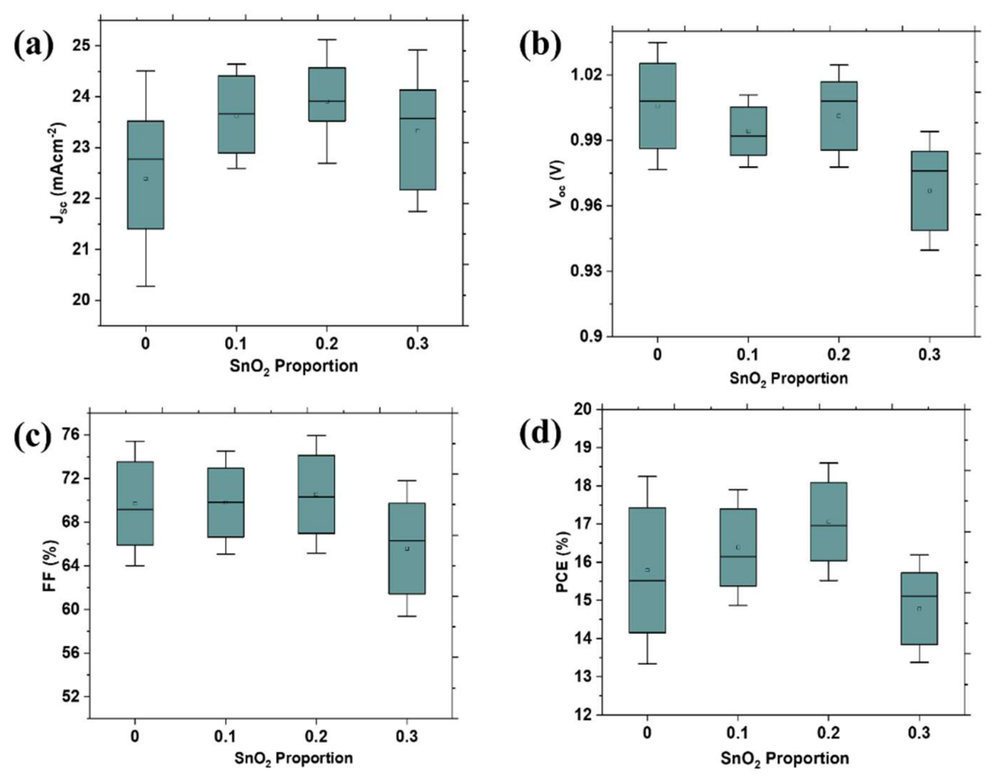
3.3. Performance Characteristics of PSCs

The photovoltaic performance of a solar cell is quantified by its PCE which is a function of the short circuit current density (Jsc), open circuit voltage (Voc) and FF. The PV performance parameters of the fabricated PSCs were determined from their J-V curves measured under illumination using a solar simulator (AM1.5, 100 mW/cm2). Figure 7a–c compares the J-V curves, Nyquist plots and the EQE curves of the control and best performing devices while Figure 7d shows the SEM cross-sectional image of the fabricated planar PSC device. It is seen from Figure 7a that the best performing device based on SnO2-TiO2 ETL with 0.2 SnO2 content had higher Jsc when compared to the control device based on TiO2. To find out the reason for the observed increase in Jsc, we carried out EIS studies on the control and the best performing PSC devices under illumination and the results are displayed by Nyquist plots shown in Figure 7b.
The Nyquist plots shows two semicircles, one in the high frequency region that is associated with the charge transfer resistance (Rtr) from perovskite to the ETL and one in the low frequency region which is associated with recombination resistance (Rrec) at the ETL/perovskite interface in the PSC device [59]. The Nyquist curves were fitted with equivalent RC circuit (inset of Figure 7b) to allow for the extraction of Rs, Rtr and Rrec. It is noticeable from Figure 7b that the incorporation of SnO2 into TiO2 leads to a reduction in both the Rs and Rtr values while the value of Rrec increased. For the device area under consideration, Rs and Rtr decreased from 5.23 Ω cm2 to 3.67 Ω cm2 and from 14.54 Ω cm2 to 12.27 Ω cm2, respectively for the control and the best performing SnO2-TiO2 based devices. On the other hand, Rrec increased from 5.37 Ω cm2 for the control device to 13.07 Ω cm2 for the SnO2-TiO2 based device. The decrease in Rs agrees with the observed improvement in σ of the ETL with SnO2 incorporation (Figure 5d). The reduction in the value of Rs in the SnO2-TiO2 based device led to an improvement in its electron transport properties. Consequently, the charge carrier collection efficiency of the PSC device based on SnO2-TiO2 ETL improved, as shown by the EQE measurement in Figure 7c.
For the different sets of PSCs fabricated, the PV parameters (Jsc, Voc, FF and PCE) were determined from their J-V curves and expressed as a function of the proportion of SnO2 in the ETL by means of statistical box plots as shown in Figure 8a–d. From the figure, we observe an increase in the mean values of Jsc, FF and PCE of the PSCs as the proportion of SnO2 in the ETL increase from 0 to 0.2. Beyond this proportion, the mean values of these PV parameters decreased. A summary of the experimentally measured PV performance characteristics is given in Table S3 in the Supplementary Materials. The trend observed in the variation of these parameters with the proportion of SnO2 in the ETL follows the same trend displayed by the σ of the ETL (Figure 5d). This indicates that σ of the ETL played a role in shaping the performance of the overall PSC device. However, the mean values of the Voc showed a general decrease with the SnO2 content in the ETL due to a possible downward shift in the conduction band edge of TiO2 when modified with SnO2 [60].

4. Conclusions

Pristine TiO2 and SnO2-modified TiO2 thin films with different proportions of SnO2 have been studied as ETLs in FA-rich planar PSCs. The results show that incorporating SnO2 in TiO2 in the right proportion improves its electrical conductivity and optical transmission of the ETL film which consequently increase the PCE of PSC. By introducing 0.2 volume proportion of SnO2 in TiO2, the PCE of the PSC increased by 7.17%. The improvement is mainly attributed to the enhancement in the electrical conductivity of the ETL and the accompanying reduction in Rs of PSC that increases the charge carrier collection efficiency and hence the PCE. The EIS results show that the values of Rs of the PSCs decrease from 5.23 Ω cm2 to 3.67 Ω cm2, when TiO2 ETL is modified with 0.2 volume proportion of SnO2. From this study, we conclude that the strategies geared reducing Rs in PSCs are beneficial in improving the PCE.

Supplementary Materials

The following are available online at https://www.mdpi.com/article/10.3390/en14237870/s1, Figure S1: EDS spectra of ETL films at different proportion of SnO2; Table S1: Bandgap and electrical conductivity of the ETL at different SnO2 content; Table S2: TRPL Bi-exponential fitting parameters and Table S3: PV performance parameters of PSCs with different SnO2 proportion in the ETL.

Author Contributions

Conceptualization, W.S., E.N. and K.O.; methodology, R.K.K., D.O. and D.M.S.; formal analysis, R.K.K., S.A., D.O. and R.I.; writing—original draft preparation, R.K.K. and D.A.; writing—review and editing, R.K.K., M.K., A.B. and K.O.; supervision, W.S., E.N. All authors have read and agreed to the published version of the manuscript.

Funding

This research was funded by PASET-RSIF and World Bank.

Institutional Review Board Statement

Not applicable.

Informed Consent Statement

Not applicable.

Data Availability Statement

The data that support the findings of this study are available from the corresponding author upon reasonable request.

Acknowledgments

The authors wish to acknowledge the PASET-RSIF and World Bank for their financial support and Worcester Polytechnic Institute for their support of this work.

Conflicts of Interest

The authors declare no conflict of interest.

References

  1. Even, J.; Boyer-Richard, S.; Carignano, M.; Pedesseau, L.; Jancu, J.-M.; Katan, C. Theoretical insights into hybrid perovskites for photovoltaic applications. Proc. SPIE 2016, 9742, 97421A. [Google Scholar] [CrossRef] [Green Version]
  2. Koech, R.K.; Kigozi, M.; Bello, A.; Onwualu, P.A.; Soboyejo, W.O. Recent advances in solar energy harvesting materials with particular emphasis on photovoltaic materials. In Proceedings of the IEEE PES/IAS PowerAfrica Conference: Power Economics and Energy Innovation in Africa, PowerAfrica 2019, Abuja, Nigeria, 20–23 August 2019; pp. 627–632. [Google Scholar] [CrossRef]
  3. Mali, S.S.; Hong, C.K. P-i-n/n-i-p type planar hybrid structure of highly efficient perovskite solar cells towards improved air stability: Synthetic strategies and the role of p-type hole transport layer (HTL) and n-type electron transport layer (ETL) metal oxides. Nanoscale 2016, 8, 10528–10540. [Google Scholar] [CrossRef]
  4. You, J.; Meng, L.; Hong, Z.; Li, G.; Yang, Y. Inverted planar structure of perovskite solar cells. In Organic-Inorganic Halide Perovskite Photovoltaics: From Fundamentals to Device Architectures; Springer: Cham, Switzerland, 2016. [Google Scholar]
  5. Thakur, U.; Kisslinger, R.; Shankar, K. One-Dimensional Electron Transport Layers for Perovskite Solar Cells. Nanomaterials 2017, 7, 95. [Google Scholar] [CrossRef] [PubMed]
  6. Yue, L.; Yan, B.; Attridge, M.; Wang, Z. Light absorption in perovskite solar cell: Fundamentals and plasmonic enhancement of infrared band absorption. Sol. Energy 2016, 124, 143–152. [Google Scholar] [CrossRef]
  7. Shi, J.; Li, Y.; Li, Y.; Li, D.; Luo, Y.; Wu, H.; Meng, Q. From Ultrafast to Ultraslow: Charge-Carrier Dynamics of Perovskite Solar Cells. Joule 2018, 2, 879–901. [Google Scholar] [CrossRef] [Green Version]
  8. Hsiao, Y.C.; Wu, T.; Li, M.; Liu, Q.; Qin, W.; Hu, B. Fundamental physics behind high-efficiency organo-metal halide perovskite solar cells. J. Mater. Chem. A 2015, 3, 15372–15385. [Google Scholar] [CrossRef]
  9. Giorgi, G.; Yamashita, K. Organic-inorganic halide perovskites: An ambipolar class of materials with enhanced photovoltaic performances. J. Mater. Chem. A 2015, 3, 8981–8991. [Google Scholar] [CrossRef]
  10. Zhang, F.; Yang, B.; Li, Y.; Deng, W.; He, R. Extra long electron-hole diffusion lengths in CH 3 NH 3 PbI 3-: X Cl x perovskite single crystals. J. Mater. Chem. C 2017, 5, 8431–8435. [Google Scholar] [CrossRef]
  11. Tailor, N.K.; Abdi-Jalebi, M.; Gupta, V.; Lu, H.; Dar, M.I.; Li, G.; Satapathi, S. Recent progress in morphology optimization in perovskite solar cells. J. Mater. Chem. A 2020, 8, 21356–21386. [Google Scholar] [CrossRef]
  12. Le Corre, V.M.; Stolterfoht, M.; Perdigo, L.; Feuerstein, M.; Wolff, C.; Bolink, H.J.; Neher, D.; Koster, L.J.A. Charge Transport Layers Limiting the Efficiency of Perovskite Solar Cells: How To Optimize Conductivity, Doping, and Thickness. ACS Appl. Energy Mater. 2019, 29, 40. [Google Scholar] [CrossRef] [Green Version]
  13. Wu, N.; Wu, Y.; Walter, D.; Shen, H.; Duong, T.; Grant, D.; Barugkin, C.; Fu, X.; Peng, J.; White, T.; et al. Identifying the Cause of Voltage and Fill Factor Losses in Perovskite Solar Cells by Using Luminescence Measurements. Energy Technol. 2017, 5, 1827–1835. [Google Scholar] [CrossRef] [Green Version]
  14. Grill, I.; Aygüler, M.F.; Bein, T.; Docampo, P.; Hartmann, N.F.; Handloser, M.; Hartschuh, A. Charge Transport Limitations in Perovskite Solar Cells: The Effect of Charge Extraction Layers. ACS Appl. Mater. Interfaces 2017, 9, 37655–37661. [Google Scholar] [CrossRef] [Green Version]
  15. Wolff, C.M.; Caprioglio, P.; Stolterfoht, M.; Neher, D. Nonradiative Recombination in Perovskite Solar Cells: The Role of Interfaces. Adv. Mater. 2019, 31, 1902762. [Google Scholar] [CrossRef] [PubMed] [Green Version]
  16. Stolterfoht, M.; Caprioglio, P.; Wolff, C.M.; Márquez, J.A.; Nordmann, J.; Zhang, S.; Rothhardt, D.; Hörmann, U.; Amir, Y.; Redinger, A.; et al. The impact of energy alignment and interfacial recombination on the internal and external open-circuit voltage of perovskite solar cells. Energy Environ. Sci. 2019, 12, 2778–2788. [Google Scholar] [CrossRef] [Green Version]
  17. Courtier, N.E.; Cave, J.M.; Foster, J.M.; Walker, A.B.; Richardson, G. How transport layer properties affect perovskite solar cell performance: Insights from a coupled charge transport/ion migration model. Energy Environ. Sci. 2019, 12, 396–409. [Google Scholar] [CrossRef] [Green Version]
  18. Ren, X.; Wang, Z.S.; Choy, W.C.H. Device Physics of the Carrier Transporting Layer in Planar Perovskite Solar Cells. Adv. Opt. Mater. 2019, 7, 1900407. [Google Scholar] [CrossRef]
  19. Mahmood, K.; Sarwar, S.; Mehran, M.T. Current status of electron transport layers in perovskite solar cells: Materials and properties. RSC Adv. 2017, 7, 17044–17062. [Google Scholar] [CrossRef] [Green Version]
  20. Yu, M.; Guo, Y.; Yuan, S.; Zhao, J.S.; Qin, Y.; Ai, X.C. The influence of the electron transport layer on charge dynamics and trap-state properties in planar perovskite solar cells. RSC Adv. 2020, 10, 12347–12353. [Google Scholar] [CrossRef]
  21. Nimens, W.J.; Ogle, J.; Caruso, A.; Jonely, M.; Simon, C.; Smilgies, D.; Noriega, R.; Scarpulla, M.; Whittaker-Brooks, L. Morphology and Optoelectronic Variations Underlying the Nature of the Electron Transport Layer in Perovskite Solar Cells. ACS Appl. Energy Mater. 2018, 1, 602–615. [Google Scholar] [CrossRef]
  22. Shin, S.S.; Lee, S.J.; Seok, S.I. Metal Oxide Charge Transport Layers for Efficient and Stable Perovskite Solar Cells. Adv. Funct. Mater. 2019, 29, 1900455. [Google Scholar] [CrossRef]
  23. Zhou, Y.; Li, X.; Lin, H. To Be Higher and Stronger—Metal Oxide Electron Transport Materials for Perovskite Solar Cells. Small 2020, 16, 1902579. [Google Scholar] [CrossRef] [PubMed]
  24. Zheng, S.; Wang, G.; Liu, T.; Lou, L.; Xiao, S.; Yang, S. Materials and structures for the electron transport layer of efficient and stable perovskite solar cells. Sci. China Chem. 2019, 62, 800–809. [Google Scholar] [CrossRef]
  25. Chen, X.; Mao, S.S. Titanium dioxide nanomaterials: Synthesis, properties, modifications and applications. Chem. Rev. 2007, 107, 2891–2959. [Google Scholar] [CrossRef]
  26. Chen, X. Titanium dioxide nanomaterials and their energy applications. Cuihua Xuebao/Chin. J. Catal. 2009, 30, 839–851. [Google Scholar] [CrossRef]
  27. Pan, X.; Yang, M.Q.; Fu, X.; Zhang, N.; Xu, Y.J. Defective TiO2 with oxygen vacancies: Synthesis, properties and photocatalytic applications. Nanoscale 2013, 5, 3601–3614. [Google Scholar] [CrossRef]
  28. Yu, J.C.; Hong, J.A.; Jung, E.D.; Kim, D.B.; Baek, S.M.; Lee, S.; Cho, S.; Park, S.S.; Choi, K.J.; Song, M.H. Highly efficient and stable inverted perovskite solar cell employing PEDOT:GO composite layer as a hole transport layer. Sci. Rep. 2018, 8, 1070. [Google Scholar] [CrossRef] [PubMed] [Green Version]
  29. Nwankwo, U.; Hong, J.A.; Jung, E.D.; Kim, D.B.; Baek, S.M.; Lee, S.; Cho, S.; Park, S.S.; Choi, K.J.; Song, M.H. Effects of alkali and transition metal-doped TiO2 hole blocking layers on the perovskite solar cells obtained by a two-step sequential deposition method in air and under vacuum. RSC Adv. 2020, 10, 13139–13148. [Google Scholar] [CrossRef] [Green Version]
  30. Belchi, R.; Habert, A.; Foy, E.; Gheno, A.; Vedraine, S.; Antony, R.; Ratier, B.; Bouclé, J.; Herlin-Boime, N. One-Step Synthesis of TiO2/Graphene Nanocomposites by Laser Pyrolysis with Well-Controlled Properties and Application in Perovskite Solar Cells. ACS Omega 2019, 4, 11906–11913. [Google Scholar] [CrossRef] [PubMed] [Green Version]
  31. Saleem, A.; Ullah, N.; Khursheed, K.; Iqbal, T.; Shah, S.A.; Asjad, M.; Sarwar, N.; Saleem, M.; Arshad, M. Graphene Oxide–TiO2 Nanocomposite Films for Electron Transport Applications. J. Electron. Mater. 2018, 47, 3749–3756. [Google Scholar] [CrossRef]
  32. Li, W.; Elzatahry, A.; Aldhayan, D.; Zhao, D. Core-shell structured titanium dioxide nanomaterials for solar energy utilization. Chem. Soc. Rev. 2018, 47, 8203–8237. [Google Scholar] [CrossRef] [PubMed]
  33. Apostolopoulou, A.; Sygkridou, D.; Rapsomanikis, A.; Kalarakis, A.N.; Stathatos, E. Enhanced performance of mesostructured perovskite solar cells in ambient conditions with a composite TiO2–In2O3 electron transport layer. Sol. Energy Mater. Sol. Cells 2017, 166, 100–107. [Google Scholar] [CrossRef]
  34. Akurati, K.K.; Vital, A.; Hany, R.; Bommer, B.; Graule, T.; Winterer, M. One-step flame synthesis of SnO2/TiO2 composite nanoparticles for photocatalytic applications. Int. J. Photoenergy 2005, 7, 153–161. [Google Scholar] [CrossRef] [Green Version]
  35. Zhen, C.; Wu, T.; Chen, R.; Wang, L.; Liu, G.; Cheng, H.M. Strategies for Modifying TiO 2 Based Electron Transport Layers to Boost Perovskite Solar Cells. ACS Sustain. Chem. Eng. 2019, 7, 4586–4618. [Google Scholar] [CrossRef]
  36. Larin, A.; Womble, P.C.; Dobrokhotov, V. Hybrid SnO2/TiO2 nanocomposites for selective detection of ultra-low hydrogen sulfide concentrations in complex backgrounds. Sensors 2016, 16, 1373. [Google Scholar] [CrossRef] [PubMed]
  37. Desai, U.V.; Xu, C.; Wu, J.; Gao, D. Hybrid TiO2-SnO2 nanotube arrays for dye-sensitized solar cells. J. Phys. Chem. C 2013, 117, 3232–3239. [Google Scholar] [CrossRef]
  38. Duan, Y.; Fu, N.; Liu, Q.; Fang, Y.; Zhou, X.; Zhang, J.; Lin, Y. Sn-doped TiO2 photoanode for dye-sensitized solar cells. J. Phys. Chem. C 2012, 116, 8888–8893. [Google Scholar] [CrossRef]
  39. Dou, M.; Persson, C. Comparative study of rutile and anatase SnO2 and TiO2: Band-edge structures, dielectric functions, and polaron effects. J. Appl. Phys. 2013, 113, 083703. [Google Scholar] [CrossRef]
  40. Guo, H.; Zhang, H.; Yang, J.; Chen, H.; Li, Y.; Wang, L.; Niu, X. TiO2/SnO2 Nanocomposites as Electron Transporting Layer for Efficiency Enhancement in Planar CH3NH3PbI3-Based Perovskite Solar Cells. ACS Appl. Energy Mater. 2018, 1, 6936–6944. [Google Scholar] [CrossRef]
  41. Li, N.; Yan, J.; Ai, Y.; Jiang, E.; Lin, L.; Shou, C.; Yan, B.; Sheng, J.; Ye, J. A low-temperature TiO2/SnO2 electron transport layer for high-performance planar perovskite solar cells. Sci. China Mater. 2020, 63, 207–215. [Google Scholar] [CrossRef] [Green Version]
  42. Liu, Z.; Sun, B.; Liu, X.; Han, J.; Ye, H.; Tu, Y.; Chen, C.; Shi, T.; Tang, Z.; Liao, G. 15% efficient carbon based planar-heterojunction perovskite solar cells using a TiO2/SnO2 bilayer as the electron transport layer. J. Mater. Chem. A 2018, 6, 7409–7419. [Google Scholar] [CrossRef]
  43. Song, S.; Kang, G.; Pyeon, L.; Lim, C.; Lee, G.Y.; Park, T.; Choi, J. Systematically Optimized Bilayered Electron Transport Layer for Highly Efficient Planar Perovskite Solar Cells (η = 21.1%). ACS Energy Lett. 2017, 2, 2667–2673. [Google Scholar] [CrossRef]
  44. Tavakoli, M.M.; Yadav, P.; Tavakoli, R.; Kong, J. Surface Engineering of TiO2 ETL for Highly Efficient and Hysteresis-Less Planar Perovskite Solar Cell (21.4%) with Enhanced Open-Circuit Voltage and Stability. Adv. Energy Mater. 2018, 8, 1800794. [Google Scholar] [CrossRef]
  45. Martínez-Denegri, G.; Colodrero, S.; Kramarenko, M.; Martorell, J. All-Nanoparticle SnO2/TiO2 Electron-Transporting Layers Processed at Low Temperature for Efficient Thin-Film Perovskite Solar Cells. ACS Appl. Energy Mater. 2018, 1, 5548–5556. [Google Scholar] [CrossRef]
  46. Wan, F.; Qiu, X.; Chen, H.; Liu, Y.; Xie, H.; Shi, J.; Huang, H.; Yuan, Y.; Gao, Y.; Zhou, C. Accelerated electron extraction and improved UV stability of TiO2 based perovskite solar cells by SnO2 based surface passivation. Org. Electron. 2018, 59, 184–189. [Google Scholar] [CrossRef]
  47. Liu, N.; Chen, M.; Yang, H.; Ran, M.; Zhang, C.; Luo, X.; Lu, H.; Yang, Y. TiO2/Mg-SnO2 nanoparticle composite compact layer for enhancing the performance of perovskite solar cells. Opt. Mater. Express 2020, 10, 157–169. [Google Scholar] [CrossRef]
  48. Mohammadbeigi, A.; Mozaffari, S.; Ghorashi, S.M.B. Yolk-shell SnO2@TiO2 nanospheres as electron transport layer in mesoscopic perovskite solar cell. J. Sol-Gel Sci. Technol. 2020, 94, 731–742. [Google Scholar] [CrossRef]
  49. Oyewole, D.O.; Koech, R.K.; Ichwani, R.; Ahmed, R.; Tamayo, J.H.; Adeniji, S.A.; Cromwell, J.; Ulloa, E.C.; Oyewole, O.K.; Agyei-Tuffour, B.; et al. Annealing effects on interdiffusion in layered FA-rich perovskite solar cells Annealing effects on interdiffusion in layered FA-rich perovskite solar cells AIP Advances. AIP Adv. 2021, 11, 65327. [Google Scholar] [CrossRef]
  50. Mohamad Noh, M.F.; Teh, C.H.; Daik, R.; Lim, E.L.; Yap, C.C.; Ibrahim, M.A.; Ahmad Ludin, N.; Bin Mohd Yusoff, A.R.; Jang, J.; Mat Teridi, M.A. The architecture of the electron transport layer for a perovskite solar cell. J. Mater. Chem. C 2018, 6, 682–712. [Google Scholar] [CrossRef]
  51. Ke, W.; Zhao, D.; Cimaroli, A.J.; Grice, C.R.; Qin, P.; Liu, Q.; Xiong, L.; Yan, Y.; Fang, G. Effects of annealing temperature of tin oxide electron selective layers on the performance of perovskite solar cells. J. Mater. Chem. A 2015, 3, 24163–24168. [Google Scholar] [CrossRef]
  52. Tauc, J.; Menth, A. States in the gap. J. Non. Cryst. Solids 1972, 8, 569–585. [Google Scholar] [CrossRef]
  53. Makuła, P.; Pacia, M.; Macyk, W. How To Correctly Determine the Band Gap Energy of Modified Semiconductor Photocatalysts Based on UV-Vis Spectra. J. Phys. Chem. Lett. 2018, 6814–6817. [Google Scholar] [CrossRef] [PubMed] [Green Version]
  54. Fassl, P.; Zhao, D.; Cimaroli, A.J.; Grice, C.R.; Qin, P.; Liu, Q.; Xiong, L.; Yan, Y.; Fang, G. Effect of density of surface defects on photoluminescence properties in MAPbI3 perovskite films. J. Mater. Chem. C 2019, 7, 5285–5292. [Google Scholar] [CrossRef]
  55. Handa, T.; Tex, D.M.; Shimazaki, A.; Wakamiya, A.; Kanemitsu, Y. Charge Injection Mechanism at Heterointerfaces in CH3NH3PbI3 Perovskite Solar Cells Revealed by Simultaneous Time-Resolved Photoluminescence and Photocurrent Measurements. J. Phys. Chem. Lett. 2017, 8, 954–960. [Google Scholar] [CrossRef] [PubMed]
  56. Jain, A.; Kumar, P.; Jain, S.C.; Kumar, V.; Kaur, R.; Mehra, R.M. Trap filled limit voltage (VTFL) and V2 law in space charge limited currents. J. Appl. Phys. 2007, 102, 094505. [Google Scholar] [CrossRef]
  57. Jin, H.; Debroye, E.; Keshavarz, M.; Scheblykin, I.G.; Roeffaers, M.B.J.; Hofkens, J.; Steele, J.A. It’s a trap! on the nature of localised states and charge trapping in lead halide perovskites. Mater. Horiz. 2020, 7, 397–410. [Google Scholar] [CrossRef] [Green Version]
  58. Liang, P.W.; Liao, C.Y.; Chueh, C.C.; Zuo, F.; Williams, S.T.; Xin, X.K.; Lin, J.; Jen, A.K.Y. Additive enhanced crystallization of solution-processed perovskite for highly efficient planar-heterojunction solar cells. Adv. Mater. 2014, 26, 3748–3754. [Google Scholar] [CrossRef]
  59. Zhang, J.; Juárez-Pérez, E.J.; Mora-Seró, I.; Viana, B.; Pauporté, T. Fast and low temperature growth of electron transport layers for efficient perovskite solar cells. J. Mater. Chem. A 2015, 3, 4909–4915. [Google Scholar] [CrossRef]
  60. Ranjan, R.; Prakash, A.; Singh, A.; Singh, A.; Garg, A.; Gupta, R.K. Effect of tantalum doping in a TiO2 compact layer on the performance of planar spiro-OMeTAD free perovskite solar cells. J. Mater. Chem. A 2018, 6, 1037–1047. [Google Scholar] [CrossRef]
Figure 1. (af): Schematics of the ETL preparation procedure.
Energies 14 07870 g001
Figure 2. SEM images of ETL with (a) TiO2 (b) 0.1 (c) 0.2 and (d) 0.3 proportions of SnO2.
Energies 14 07870 g002
Figure 3. (a) SEM and (b) EDS Cross-sectional image of representative ETL film on FTO-coated glass; (c) XRD patterns of the ETL films (d) FWHM for the ETLs at different SnO2 content.
Energies 14 07870 g003
Figure 4. SEM images of perovskite films deposited on the different ETLs: (a) TiO2 (b) 0.1 (c) 0.2 and (d) 0.3 proportion of SnO2.
Energies 14 07870 g004
Figure 5. Optoelectronic Behavior of ETLs films: (a) Transmittance, (b) Tauc plot from absorbance (c) Dark I-V curves of the films and (d) Electrical conductivity.
Energies 14 07870 g005
Figure 6. Optical properties of perovskite films for different volume proportion of SnO2: (a) UV-Vis absorbance spectra (b) PL spectra, (c) J-V curves of electron only devices and (d) TRPL spectra of perovskite films on different ETL.
Energies 14 07870 g006
Figure 7. (a) J-V curves; (b) Nyquist curves and (c) EQE curves of the control and the best performing PSC devices (d) Cross-sectional image of the fabricated planar PSC.
Energies 14 07870 g007
Figure 8. Box plots showing the variation of (a) Jsc (b) Voc (c) FF and (d) PCE with SnO2 content in the ETL.
Energies 14 07870 g008
Publisher’s Note: MDPI stays neutral with regard to jurisdictional claims in published maps and institutional affiliations.

