Article

Pulse-Width Modulation Template for Five-Level Switch-Clamped H-Bridge-Based Cascaded Multilevel Inverter

by
Charles Ikechukwu Odeh
1,
Dmytro Kondratenko
2,*,
Arkadiusz Lewicki
2,
Marcin Morawiec
2,
Andrzej Jąderko
3 and
Janusz Baran
3
1
Department of Electrical Engineering, University of Nigeria, Nsukka 410001, Nigeria
2
Faculty of Electrical and Control Engineering, Gdańsk University of Technology, Narutowicza 11/12, 80-233 Gdańsk, Poland
3
Faculty of Electrical Engineering, Czestochowa University of Technology, 42-201 Czestochowa, Poland
*
Author to whom correspondence should be addressed.
Energies 2021, 14(22), 7726; https://doi.org/10.3390/en14227726
Submission received: 31 October 2021 / Revised: 12 November 2021 / Accepted: 16 November 2021 / Published: 18 November 2021
(This article belongs to the Special Issue Digital Signal Processing in Power Electronics Control Circuits)

Abstract

:
This article presents a carrier-based pulse-width modulation (PWM) template for a 5-level, H bridge-based cascaded multilevel inverter (MLI). The developed control concept generates adequate modulation template for this inverter topology wherein a sinusoidal modulating waveform is modified to fit in a single triangular carrier signal range. With this modulation approach, classical multiplicity and synchronization of the triangular carrier signals criterion for the extension of sinusoidal pulse-width modulation, SPWM, to several cascaded 5-level, H-bridge-based MLI topology are removed. The proposed template can be used on the inverter configuration of any level with no further control modification. Nearly even distribution of switching pulses and equalized individual cascaded cell output power were achieved with the proposed modulation scheme. Three 5-level, H-bridge-based MLI units were cascaded for 1-phase, 13-level inverter operation; simulation and experimental results are adequately presented.

1. Introduction

The green energy revolution [1], has prompted great improvements in the power-processing circuit configurations and their respective control schemes in the field of power electronics. This technological revolution aims at achieving sustainable electrical power generations and uses. Regarding this, dc to ac converters (inverters) are essential power electronics components used in many important areas such as high-voltage direct-current (HVDC) transmission [2,3], Flexible AC Transmission Systems (FACTS) [4,5], renewable energy grid integration [6,7], railway and vehicle traction [8,9], energy storage systems [10], marine propulsion [11], etc. Specialized kinds of inverters, called the multilevel inverters (MLIs), for these applications are precisely configured and designed to meet the operational output power quality requirements of the targeted applications [12].
MLI power circuit configurations have been the dominant research topic in the literature [13,14], as a reflection of the innate capabilities of this type of inverters and their influences on many industrial applications. These newly evolved MLI configurations have their operational concepts from those of the traditional MLIs: cascaded H- bridge (CHB), diode-clamped and capacitor-clamped (flying capacitor) multilevel inverters. Among these three, the CHB MLI is the only configuration that did not involve split capacitor banks. Most used configurations of the diode-clamped and capacitor-clamped multilevel inverters have been restricted to the synthesis of three-level output voltage waveforms because of input voltage deviations. These 3-level inverter configurations have reached industrial maturity and are mass-produced to serve needs of varying degrees. Comparably, the CHB MLI does not have this output voltage level restriction. Hence, modular and scalable design approach are the most cherished features of this type of inverter. Its improved output power quality makes it the best candidate for high-voltage/power deployment [12].
In Figure 1, phase legs of the two-variant configuration of the 3-level diode-clamped (Neural-Point-Clamped, NPC) MLI are shown. The traditional diode-clamping conceptual topology of the inverter output voltage is depicted in Figure 1a. Quest for active-clamping of the inverter output voltage to the neutral point, n, resulted in the power circuit configuration in Figure 1b. This power circuit is popularly called the T-type NPC inverter. Both power circuit variants have same number of active power switches, but the blocking voltage rating of two switches is compromised in the diode-free T-type topology.
In recognition of the topological features of CHB MLI that made it a better option for medium and high-voltage applications, T-type 3-level phase-leg configuration was extended to a single-phase system where optimization of the inverter switch count was achieved [15]. The supposed two bidirectional clamping switches for the 2-phase legs were reduced to one. This results in the power circuit of Figure 1c where a bidirectional clamping switch is attached to the normal H-bridge inverter. In effect, instead of generating 3-level output voltage waveform, the modified H-bridge inverter synthesizes 5-level output waveform per cycle. The works in [16,17] extended this 5-level inverter power circuit to cascaded configurations for single- and three-phase inverter systems, respectively. The single-phase cascaded structure is shown in Figure 2.
For the control of H-bridge unit cell derived MLI topologies, the triangular carrier-based sinusoidal pulse-width modulation, SPWM scheme is the popularly used modulation strategy [18]. The modulation principles entail comparing a triangular carrier wave (at high frequency) with a sinusoidal modulating signal (at fundamental frequency). As a result, this modulation scheme does not involve intricate computational requirement. Additionally, its extension to multilevel and/or multiphase systems demands only a multiplicity of the carrier and modulating waveforms.
For the control of H-bridge derived cascaded MLI configurations, two variants of the SPWM control strategy are mostly used [18]: Level-shifted, LS, and Phase-shifted, PS, PWMs. Sub-variants of the LS PWM include in-phase disposition (IPD), alternative phase-opposite-disposition (APOD), etc. The best harmonic profile of the inverter output voltage waveform is provided by the in-phase disposition, IPD, PWM. The harmonic performance of the APOD is same with that of PS SPWM [19,20]. The PS PWM scheme provides nearly equal gating signals to all the power switches in the series inverter units. Consequently, nearly equal power is delivered from each of the cascaded cells. In attempts to combine these good control characteristics in IPD and PS PWM techniques, the works in [21,22,23] presented modulation approaches for this PWM combinational concept.
Appropriate arrangement of many carrier waves is the base concept for extending SPWM to a series of output voltage levels in each inverter phase. Each carrier wave is responsible for the generation of an output voltage level in all phases of the inverter. In an application where there is the need for the synthesis of many inverter output voltage levels, marching number of carrier waves in both conventional LS and PS SPWM techniques for this MLI configuration is unavoidable. Moreover, proper synchronization of this number of carrier waves dictates the quality output voltage waveforms from the MLI system. The synchronization is impeded by memory limitations of the control platform, sampling issues, and computational delays. In real-time SPWM digital control of CHB MLI, these issues lead to poor dynamic performance [24,25,26].
In a research effort to remove this traditional need for many carrier signals in SPWM, Ronanki and Williamson in [27] presented a SPWM strategy whereby the modulating wave is made to fit in a positively single carrier range. With this modulation waves arrangement, generation of multi-level output voltage waveforms at the inverter output is feasible. This modulation approach was targeted to the control of the modular multilevel converter, MMC. Particularizing this control approach to CHB MLI adaptation, the work in [28] proposed a modified SPWM scheme. In this work, it was shown that IPD SPWM scheme could be used in the control of CHB MLI with a single carrier signal; independent of the number cascaded H-bridge cells. However, it is obvious that this modulation scheme still possesses the undesirable features of IPD SPWM: non-distribution of switching signals among the power switches and uneven power delivery from the inverter units. In view of these drawbacks, a single carrier-based pulse-width modulation template for cascaded H-Bridge multilevel inverters was proposed in [29]. Therein, a generalized modulation approach that uses a carrier signal was presented. This is easily adaptable to any number of cascaded H-bridges without modification of the logic control circuit.
Considering the 5-level switch-clamped inverter in Figure 1c, the work in [30] modified the classical level-shifted SPWM in the synthesis of 5-level output voltage waveform. The modification is seen in the use of two off-set rectified sine waves and a single carrier. The offset has the effect of reducing the supposed two positively carrier signals to one in the positive half-cycle; and the rectification eliminates the supposed two negatively carrier signals in the negative half-cycle. If this approach is extended to many single-phase T-type inverters in series, the inherent characteristic of multiplicity of carrier signals and non-equalization of gating pulses to the corresponding semiconductor switches in the cascaded units are inevitable.
In view of these, this paper presents a simplified pulse-width modulation template for five-level switch-clamped H-bridge-based multilevel inverter shown in Figure 2. Its operational concept, as in [27,29], is obtained from the principle of IPD PWM. Herein, the modulating signal is changed to be in a positively single carrier waveform range so as to synthesize the required output waveform template for the control of the MLI configuration. The drawbacks of this IPD PWM are removed from the modulation scheme by a reverse-voltage-sorting algorithm. Consequently, this control approach can be viewed as a hybrid modulation scheme that is in-between the phase- and level-shifted carrier-based SPWM techniques. It inherits the good characteristics in these two modulation schemes. Demonstrations in simulation and experimental results are shown for a three-cell cascaded configuration of Figure 2.
The rest of this article is organized as follows. Section 2 presents the inverter configuration and switching scheme. A step-by-step presentation of the proposed single carrier sinusoidal pulse-width modulation scheme for 5-level switch-clamped multilevel inverter is given in Section 3. Simulation and scaled-down experimental results are presented in Section 4. Finally, Section 5 concludes this article.

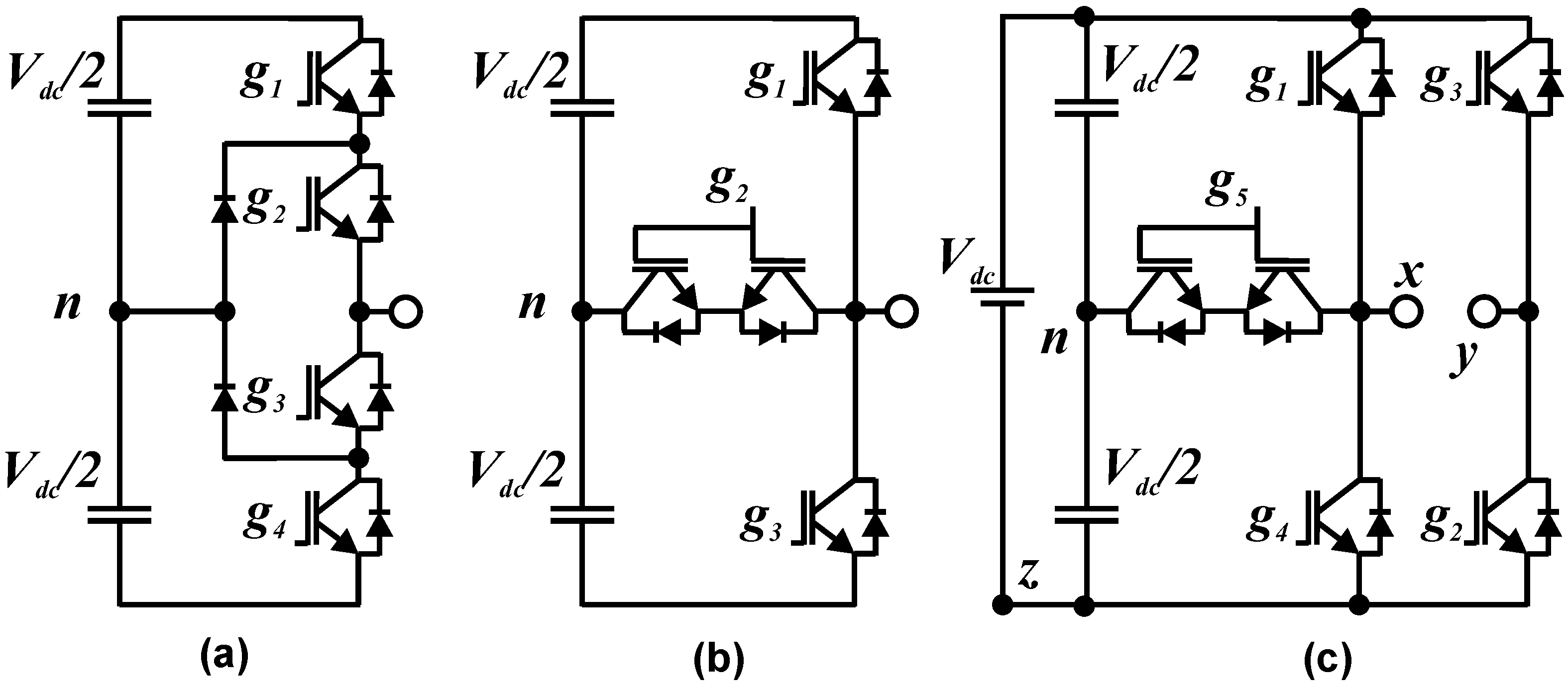
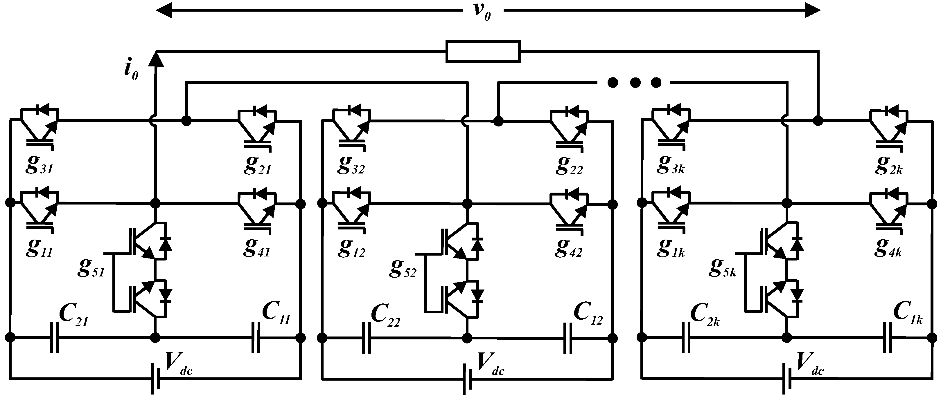
2. Five-Level Switch-Clamped Inverter

With the 5-level switch-clamped inverter unit cell of Figure 1c, the cascaded MLI under study is configured as shown in Figure 2. All the cascaded inverter units have a split capacitor bank with isolated dc-link. Appreciable high output voltages can be generated from this power circuit by just raising the number of cascaded unit cells; the voltage rating of the components remaining the same. In Figure 1c, g1, g2, g3, g4 and g5 are the gating pulses of the power switches. These pulses are of value 1 if their corresponding switches are closed and 0 otherwise. They are the switching states of the active power devices. With reference to node z, the output voltage (vxz) of the first leg of the inverter (node x) is pulse width modulated; while a square wave output voltage (vyz) with 0.5 duty-cycle, amplitude of v d c and at the fundamental frequency is synthesized at the output terminal of the second inverter leg (node y). This implies that g2 and g3 have 1 and 0 values, respectively, in the positive half-cycle and 0 and 1 otherwise. With reference to node z and in both half-cycles, 0 ,   0.5   V d c   a n d   V d c voltage levels are synthesized at node ‘x’. The possible five binary combinations of g1, g2, g3, g4 and g5 and corresponding synthesized output voltages of the 5-level inverter in Figure 1c are typified in their logic truth-table representation in Table 1. It is obvious in this Table that at any switching instant only two switches are turned on.

3. Proposed Single Carrier SPWM for 5-Level Switch-Clamped Multilevel Inverter

In this proposed modulation strategy, the multi-carrier signals in IPD PWM are virtually represented by a single carrier. In such arrangement, the contiguous bands occupied by these multi carriers in the conventional LS SPWM is still conserved. The concept of this modulation scheme is anchored on the generation of multilevel waveform template, MWT, from which the gating pulses of the power switches in each inverter units are derived. Herein, it is acknowledged that the synthesis of this MWT involves already known facts about this inverter configuration; as documented in the literature. In the following subsections, detailed information on the MWT creation is given by referring to Figure 3.

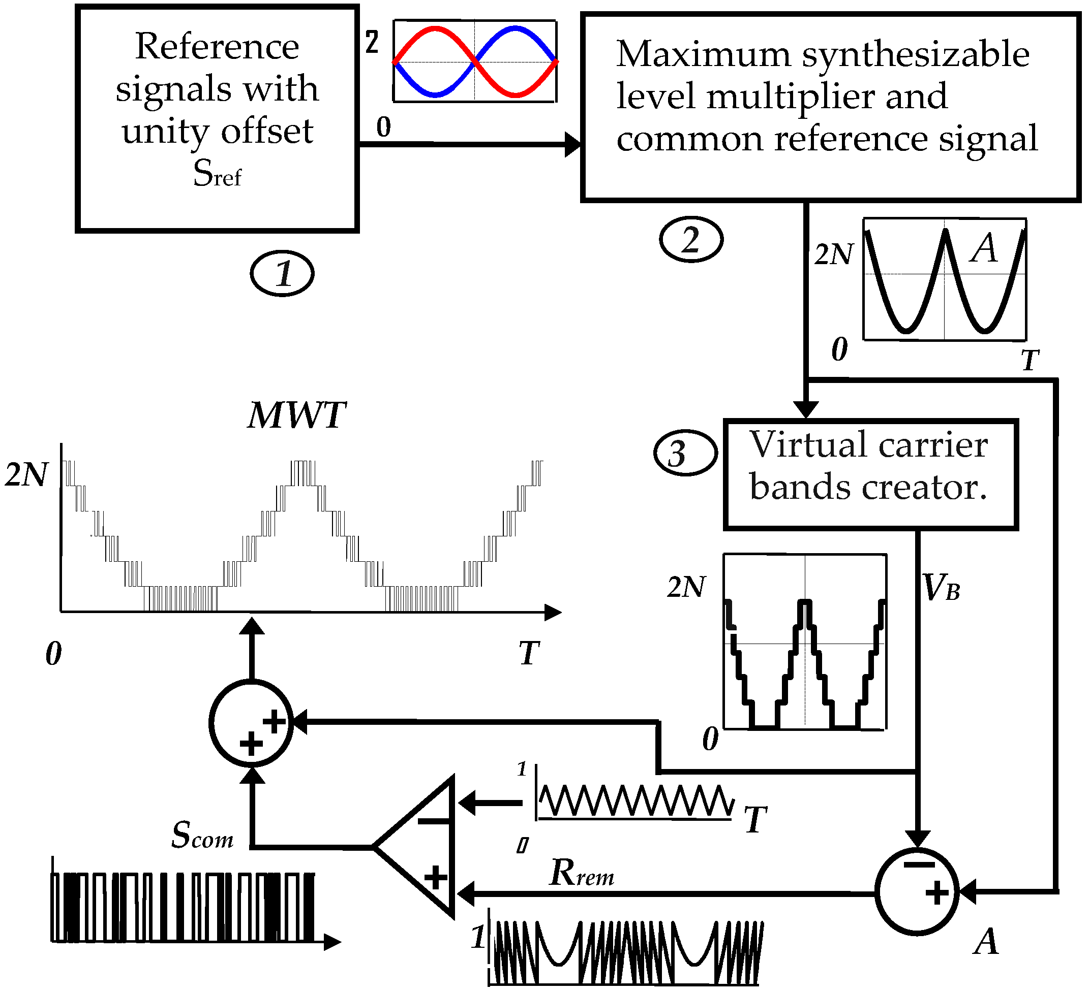
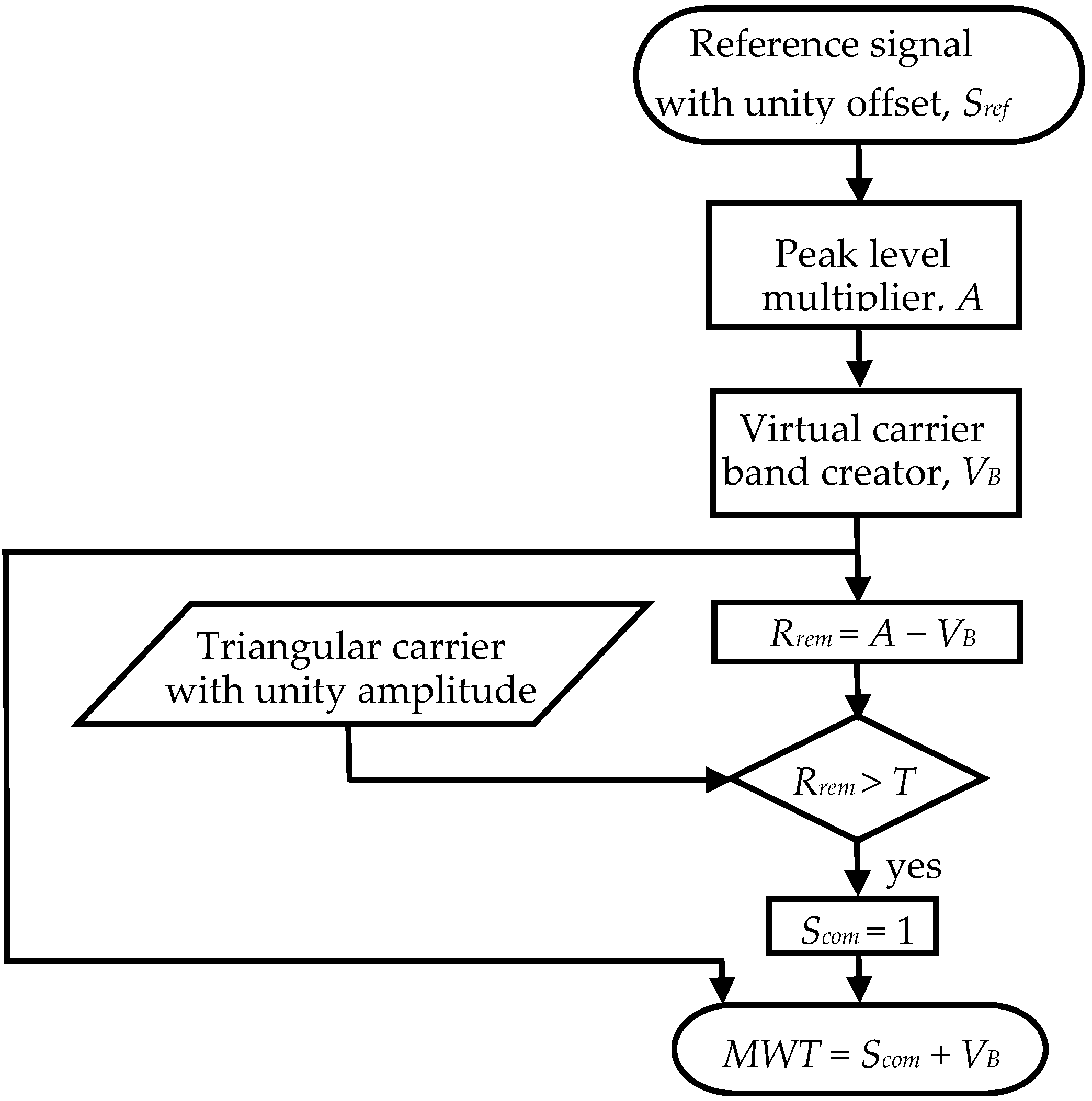
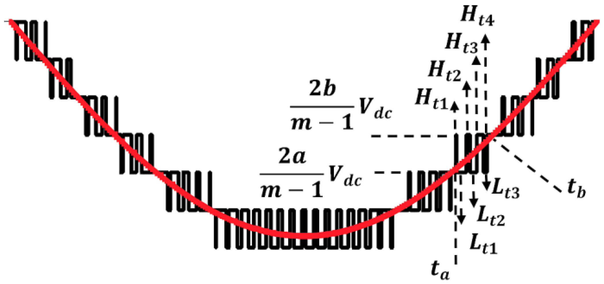
3.1. Reference Waveform Generation

The base sinusoidal signal of the modulation scheme is generated in blocks 1 and 2 in Figure 3. Two complementary unity-off-set sine signals are generated in block 1; whose frequency is the base/fundamental output frequency. The work in [31] gave the expression for the highest number of possible inverter leg voltage levels, Nmax, in a MLI configuration in terms of two indices. In this referred work and also in [32], this concept was demonstrated. A recap of this expression is given in Equation (1),
N m a x = y = 1 z V y ( m y 1 )  
Vy is the per unit voltage step; my is the number of voltage levels generated by the yth series unit, for each half-cycle. Referring to Figure 2, it is obvious that all the cascaded inverter units generate waveforms with the same voltage step since they are symmetrically connected. Hence, V 1 = V 2 =   V z = 1 . Moreover, the number of voltage levels ( 0 ,   0.5 V d c ,   V d c ) generated in any of the cascaded inverter cell per half cycle is equal ( m 1 = m 2 =   m z = 3 ) . Therefore, Equation (1) becomes
N m a x = 2   ( Number   of   cascaded   five level   inverter   cells )  
The output of block 1 is multiplied by this factor, which is generated in block 2, giving the expression in Equation (3).
A p o s = N m a x [ 1 + m s i n ( ω t ) ]
A n e g = N m a x [ 1 m s i n ( ω t ) ]  
m is the modulation index and ω is the angular frequency of the reference waveforms; pos and neg indicate the positive and negative half cycles, respectively; Apos and Aneg are the positive and negative reference signals with unity offset. A common reference signal, A, for both half cycles is obtained by taking the minimum function value of Apos and Aneg, as given in Equation (5),
A = min ( A p o s ,   A n e g )
In block 2, Equation (5) is implemented.

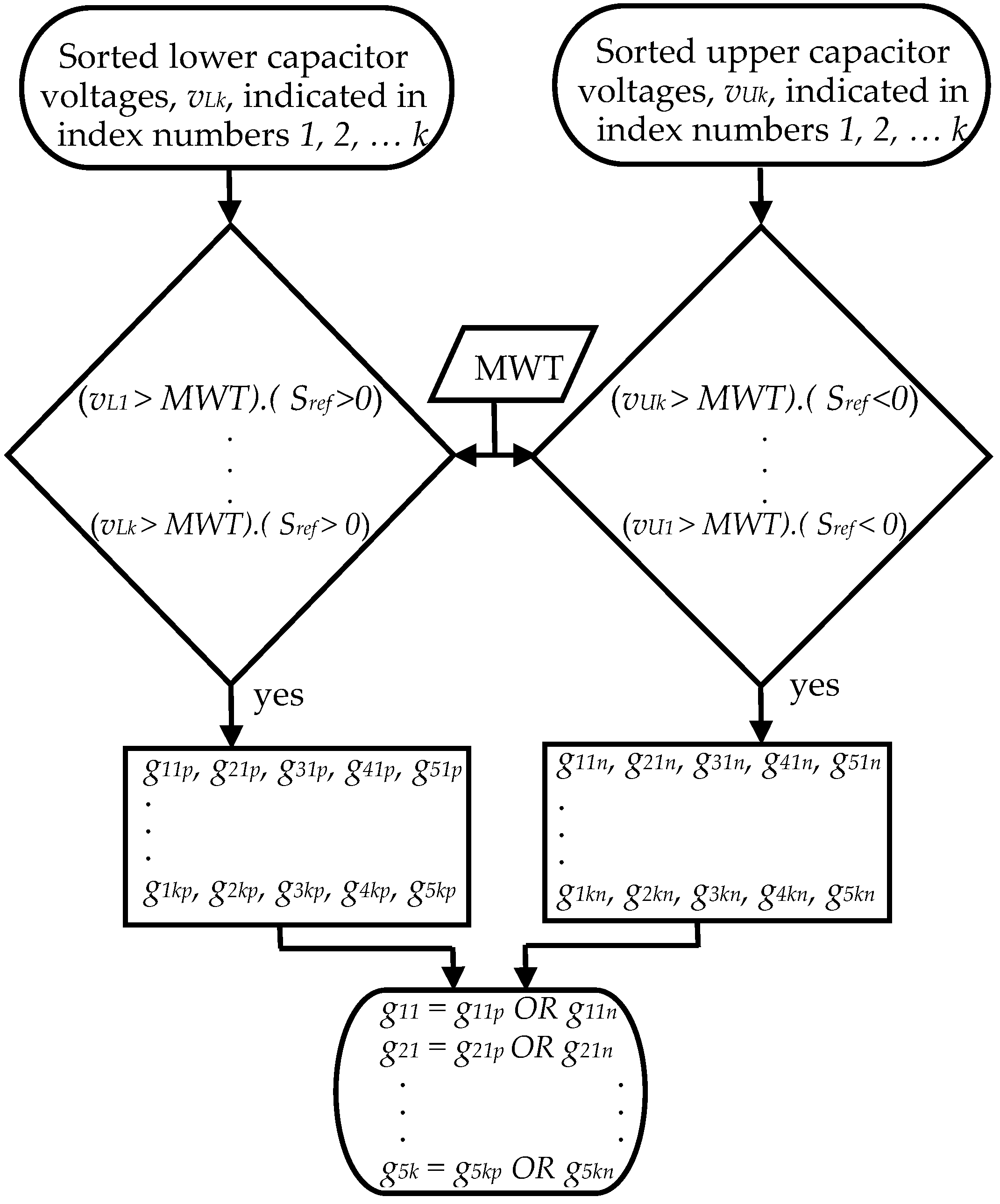
3.2. Generation of the Virtual Carrier Bands

Virtual carrier band creation is the main issue at stake in the concept of single carrier SPWM technique. Understanding of the virtual carrier band creation concept was detailed in [29] for CHB MLI. The sequential constant levels of comparisons form the virtual carrier bands in this modulation scheme for cascaded 5-level MLI. For the inverter configuration shown in Figure 2, the inverter leg reference signal is given in Equation (5). This signal is compared with specified number of constants; the xth comparison level for the zth cascaded inverter units, Cz, is given by
C z = { [ y = 1 z 1 ( m y 1 ) V y ] + ( x 1 ) V z } x = 1 , 2 ,   m z 1
As mentioned previously, m y = m z = 3 ; this necessitates the comparison level, x, to have value of 1 and 2. Explanation of Equation (6) can be done by taking only two 5-level inverter units, per phase in Figure 2, for an instance. In Equation (6), it is obvious that C 2 = 2   a n d   3   a n d   C 1 = 1 . In [31,32], step modulation within the virtual bands formed by these constants was deployed; herein, the floor function is used on the common reference waveform, A. This operation yields a stepped waveform, VB; this waveform provides information on the virtual carrier bands in terms of numerical integers (1, 2, 3…).
V B = f l o o r ( A ) = f i x ( A )
VB can be seen as a calculated stack of the virtual carrier bands wherein the actual real carrier signals are absent. With such perception, the cascaded inverter system needs to be modulated; the modulating waveform, Rrem, is obtained by subtracting VB from A.
R r e m = A V B
Comparison of Rrem with a single triangular carrier signal, T, yields pulse train, Scom.
S c o m = R r e m > T
The multilevel waveform template for the 5-level inverter system, MWT, is generated by adding the two waveforms, VB and Scom.
M W T = V B + S c o m
The flowchart that shows all the necessary steps for generating MWT waveform is depicted in Figure 4.
Step-by-step derivation of the gating signals to the power switches is given in the flowchart of Figure 5.
Positive and negative half cycles of the reference signal, Sref are considered in the input capacitor voltage balancing. The upper and lower capacitor voltages in each cell are sorted in ascending order of magnitude and indexed accordingly in the order of the cells notations in Figure 2, (that is: cell k has switches g1k, g2k, g3k, g4k, g5k; and its sorted upper and lower capacitor voltage are denoted as vUk and vLk, respectively). The sorted indexed lower and upper capacitor voltages, vUk and vLk, from each cell are compared with the derived MWT waveform in the positive and negative half cycles of the reference signal, Sref. These comparisons generate the respective half cycles gating pulses g1kp, g2kp, g3kp, g4kp, g5kp and g1kn, g2kn, g3kn, g4kp, g5kn; where p and n denote positive and negative half cycles. Then, the half cycles gating pulses g1kp, g2kp, g3kp, g4kp, g5kp and g1kn, g2kn, g3kn, g4kp, g5kn are combined with the logical OR to generate the corresponding full-cycle switching signals to the power switches

4. Simulation and Experimental Results

Simulation and experimental studies on the presented modulation scheme for a 13-level, multilevel inverter are carried out in this section. In the simulation study, the three 5-level inverter units are series-connected and controlled by the conventional SPWM strategies and then the proposed single carrier modulation scheme, in turn. Their respective performances in terms of the number of modulation signals requirement, THD value of the synthesized output voltages, and the sharing of gating pulses among the power switches in the cascaded inverter units are comparatively viewed. The resulting deductions from the proposed modulation model of the proposed modulation approach are experimentally verified with a laboratory prototype of the MLI inverter.

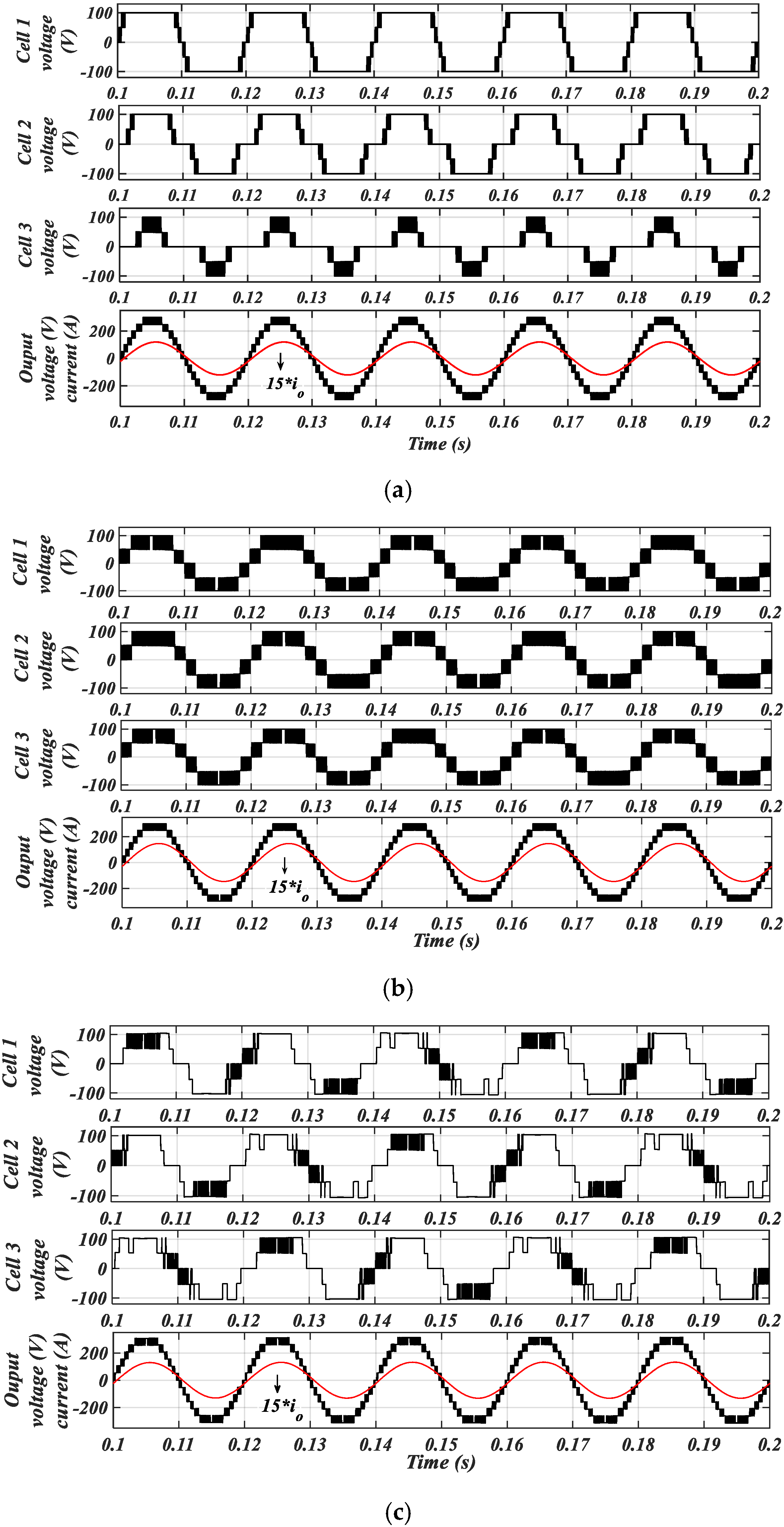
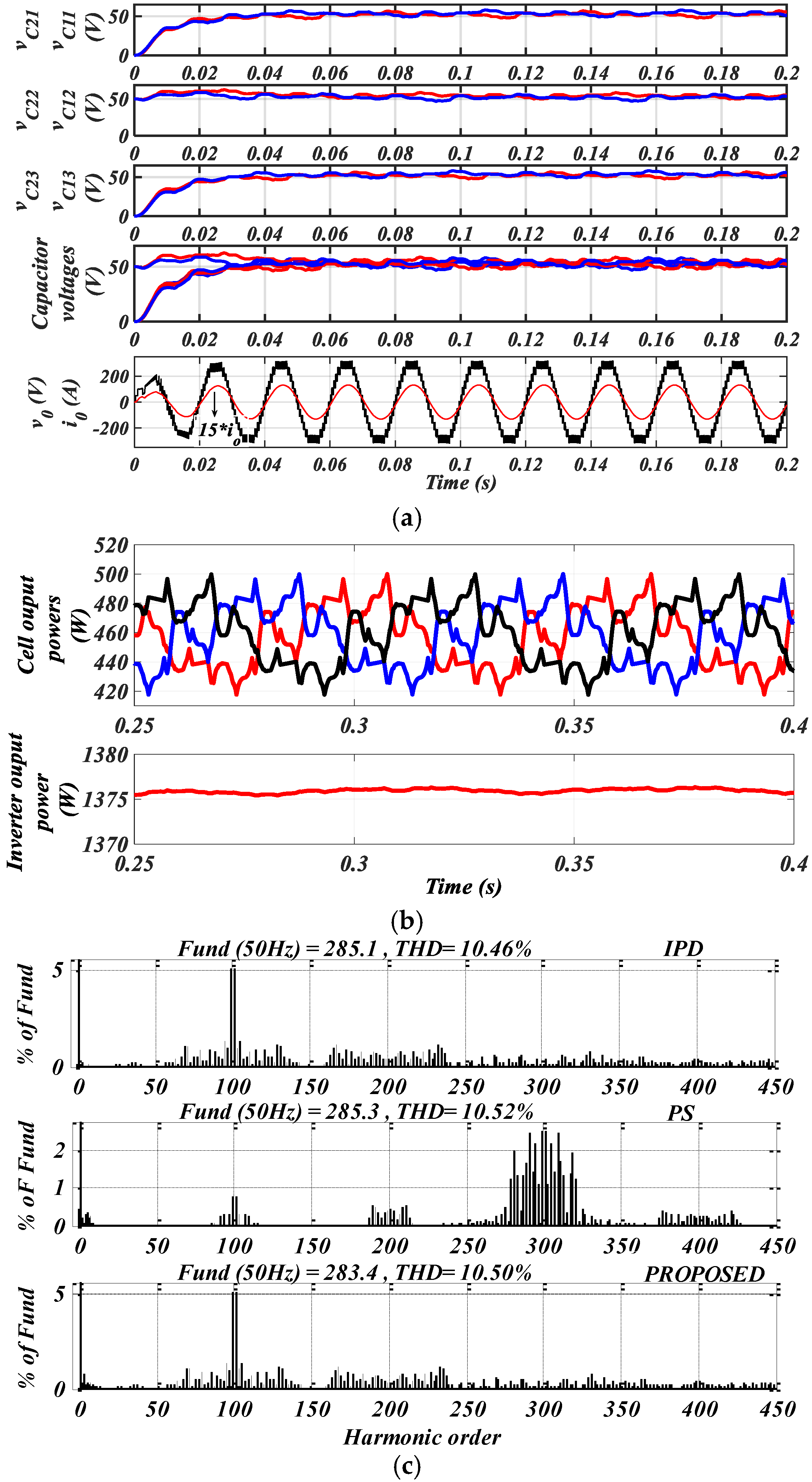
4.1. Simulation Results

The MATLAB/SIMULINK and PLECS simulation models of the power circuit shown in Figure 2 were created following the modulation outlines in Figure 4 and Figure 5. Three cascaded 5-level inverter units in Figure 2 have been selected for the simulation study. Each unit has dc-link voltage of 100 V; with splitting capacitor banks of capacitance 2200 µF each. Series 35 Ω resistor and 20 mH inductor form the inverter load. The inverter switching frequency is 5 kHz.
Shown in Figure 6a,b are the procedural modulation waveforms of the control schemes used in [16,17] for three cascaded 5-level inverter units. Both are modified traditional in-phase disposition and phase-shifted SPWM techniques wherein rectified modulating signal is used to reduce the number of triangular carrier waves. The proposed single carrier SPWM waveform template for the same inverter configuration is displayed in Figure 6c. It is obvious in Figure 6a,b that the control pulses to the power switches are obtained by fixed referential comparison of the modulation waveforms in order to generate the output voltage waveform. However, in Figure 6c, the reverse is the case. The output voltage waveform template is first generated and the gating pulses are obtained by referring to this generated template. Certain control options can be built in while such a reference is made. The two-fold advantage of this SPWM approach is: first, the single triangular carrier wave used in creating the MWT is insensitive to the number of cascaded inverter units, as detailed earlier in Figure 3; secondly, the input split capacitor bank voltages can be controlled since their dynamic value variations can be optional inputs while referring to the modulation template. Comparison of this modulation strategy with the traditional SPWM schemes is given in Table 2.
In all the modulation schemes deployed, the same power circuit and modulation parameter values were used. The depth of modulation was 0.95. First, the IPD and PS traditional SPWM schemes were applied in turn. The expected respective inverter output waveforms are shown in Figure 7a,b. Secondly, the proposed PWM approach was applied and the generated inverter input and output variable waveforms are displayed in Figure 7c. In this figure, it is clear that nearly evenly distributed output voltage pulses were obtained in each of the three cascaded inverter units.
The synthesized individual cell 5-level output voltages stacked appropriately to yield the overall 13-level output voltage and the corresponding sinusoidal load current waveforms. Considering an unbalanced situation at star-up with different initial voltage conditions of the splitting capacitor banks: v C 11 = 10   V , v C 21 = 0   V ,   v C 12 = 70   V ,   v C 22 = 60   V , v C 13 = 0   V ,   and   v C 13 = 0   V .
Figure 8a displays the dc-link capacitor voltage variations in the three cells of the inverter with the generated output voltage and current waveforms. These waveforms show that all capacitor voltages in the series inverter units are balanced by the deployment of the switching strategy algorithm in Figure 5. This effective balancing is irrespective of the different initial voltages on the dc-links of the cascaded inverter cells at start-up.
The pictorial view of the individual cascaded cells output powers are given in Figure 8b. Therein, the overall inverter output power is also shown. Since the same load current flows through the three cascaded cells, this figure reveals also that the powers in each of the cells are balanced. The output voltage FFT analyses of the three considered modulation schemes are displayed in Figure 8c. In this figure, total harmonic distortion (THD) values of 10.46%, 10.52%, and 10.50% were obtained for IPD, PS and proposed modulation approach, respectively.

4.2. THD of the Inverter Output Voltage

Train of pulses in one step of inverter output voltage waveform is shown in Figure 9. Higher a and lower b voltage levels are considered; but without loss of generality, other voltage levels can be considered provided that a voltage step is realized ( a ,   b = 0 ,   1 ,   2 ,   ,   m 1 ) .   H t 1 ,   H t 2 ,   H t 3   and   H t 4 are the time durations of the pulse-width of the pulse trains at higher voltage level a; L t 1 ,   L t 2   a n d   L t 3 are the corresponding time durations at lower voltage level b. The total time durations of the pulse-width of the pulse trains at these two voltage levels are functions on a and b, given as
N H a ( a , b ) = H t 1 + H t 2 + H t 3 + H t 4
N L b ( a , b ) = L t 1 + L t 2 + L t 3
For a given modulation index, Ma, the reference sine wave at fundamental frequency, ω 0 , is correspondingly equal to the magnitudes of the per unitized voltage levels a and b, then
t a = 1 ω 0 s i n 1 ( 2 a M a ( m 1 ) )
t b = 1 ω 0 s i n 1 ( 2 b M a ( m 1 ) )
The time interval ta − tb is equal to the sum of the total time durations of the pulse-width of the pulse trains; hence
N H a ( a , b ) + N L b ( a , b ) = t b t a
N H a ( a , b ) 2 a ( m 1 ) V d c + N L b ( a , b ) 2 b ( m 1 ) V d c t b t a = M a V d c t a t b sin ( ω 0 t ) d t t b t a
From Equations (15) and (16), N H a   and N L b are obtained as
N H a ( a , b ) = { ( M a ( m 1 ) 2 ) { cos ( ω 0 t a ) cos ( ω 0 t b ) } + a { ω 0 t a ω 0 t b } }
N L b ( a , b ) = { ( M a ( m 1 ) 2 ) { cos ( ω 0 t b ) cos ( ω 0 t a ) } + a { ω 0 t b ω 0 t a } }
The root mean square, v o ,   r m s , and total harmonic distortion, v o ,   T H D expressions of the inverter output voltage are given in Equations (19) and (20), respectively.
v o ,   r m s = 2 π { { a = 0 a m 1 [ N L a ( a , b ) ( 2 a m 1 V d c ) 2 + N H b ( a , b ) ( 2 ( a + 1 ) m 1 V d c ) 2 ] } + N L b ( a m , M a ( m 1 ) 2 ) ( 2 a m m 1 V d c ) 2 + N H a ( a m , M a ( m 1 ) 2 ) ( 2 ( a m + 1 ) m 1 V d c ) 2 } 1 2
v o ,   T H D = V r m s 2 ( M a V d c 2 ) 2 M a V d c 2
Please note that a m = 0 ,   1 ,   2 ,   3 ,   should satisfy the following condition regarding the modulation index, M a ,
M a ( m 1 ) 2 1 a m < M a ( m 1 ) 2

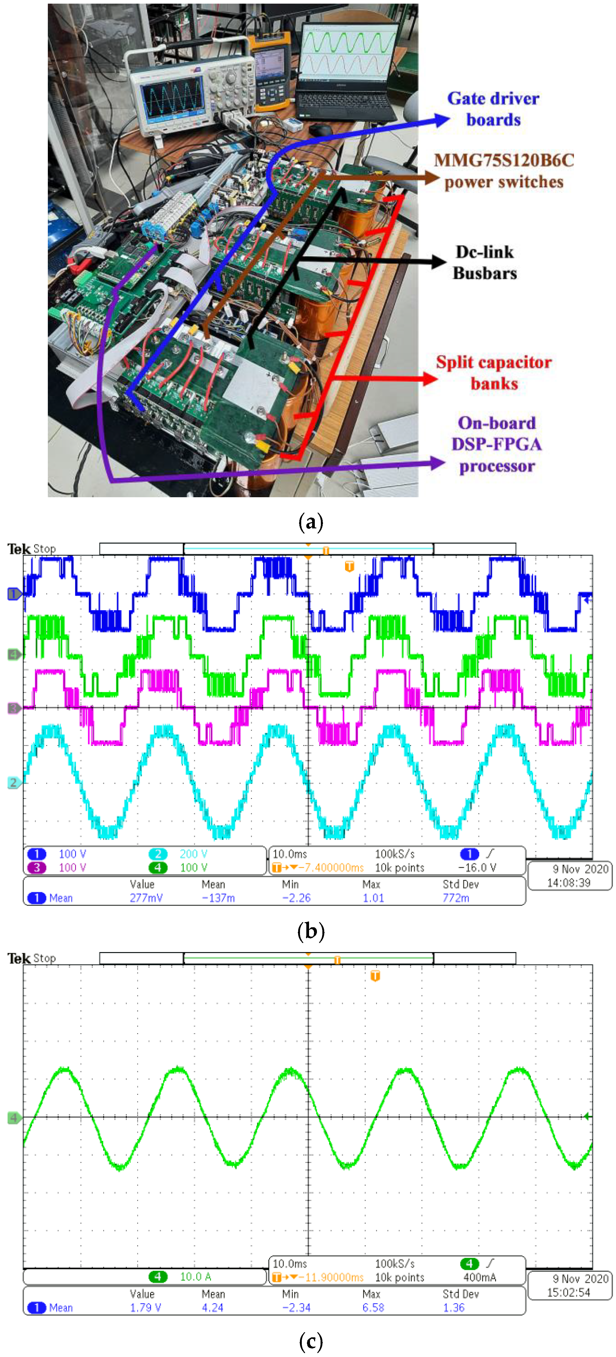
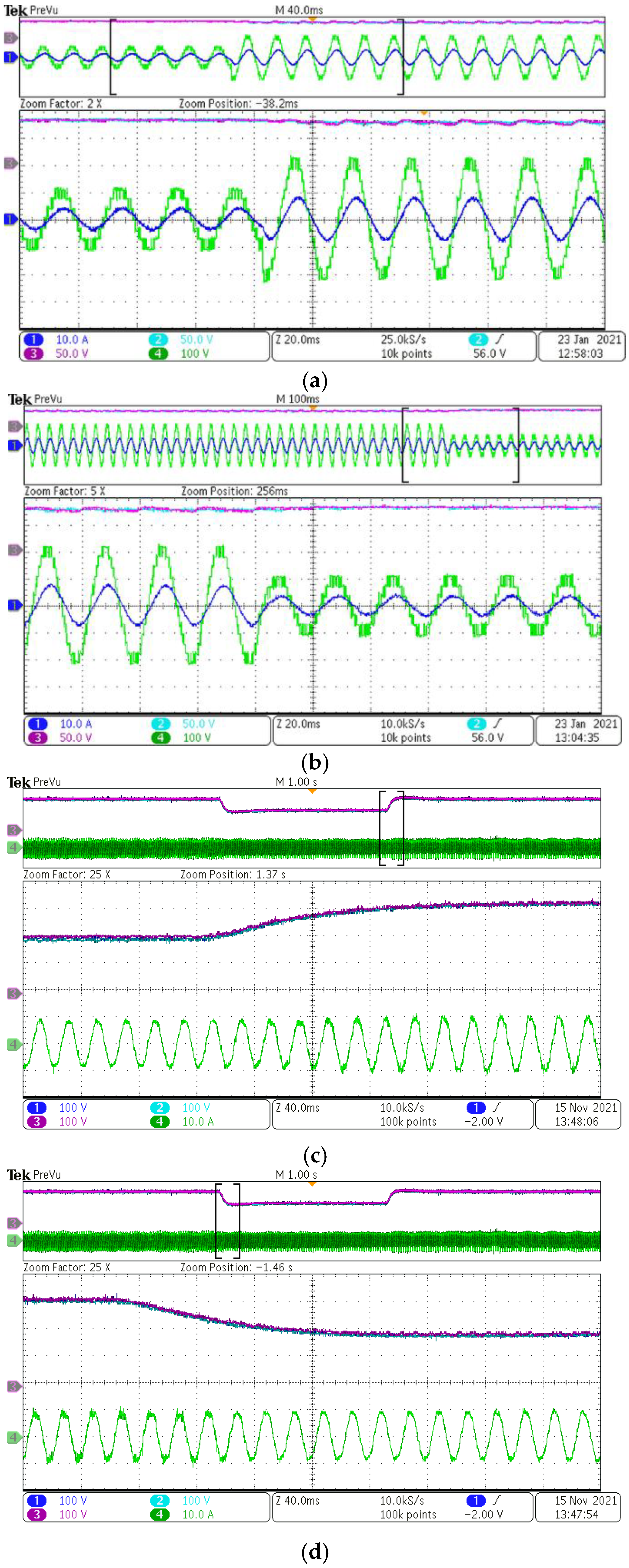
4.3. Experimental Results

The laboratory setup of the cascaded three units of 5-level MLI is shown in Figure 10a. PWM gating pulses for the power switches were generated using an on-board Digital signal processor, ADSP21363L and Altera Cyclone II FPGA. In Table 3, the laboratory inverter setup parameters are specified.
As in the simulation study, each of the three inverter units has dc-link voltage of 100 V. Operational modulation index value of 0.95 was chosen. In Figure 10, measured experimental inverter input and output voltages, powers and the corresponding load current waveforms are displayed. In comparison with the inverter simulated input and output waveforms in Figure 7c, the inverter experimental waveforms in Figure 10 are correspondingly are at par with the those from the simulation study. As shown in each of the experimental output voltages of the cascaded inverter cells, the proposed modulation approach impacts nearly equal gating pulses to the comprising power switches in each of the cells. This, as indicated in the introductory section, results in almost equal output voltage waveforms. Since same load current flows through these cells, nearly equal distributed power is handled by each of the cascaded cells. Moreover, the proposed dc-link voltage balancing algorithm in Figure 5 is experimentally demonstrated and shown in the overall output voltage waveform of the inverter. Each of the 5-level output voltages of the cells stacked appropriately to yield the 13-level inverter output voltage.
Experimental input and output powers of the inverter prototype were measured with Fluke-434-435 power-quality-analyzer and power analysis application module MDO3PWR in MDO3034 oscilloscope. Figure 11 shows the measured capacitor bank voltages and the overall inverter output voltage; output and input powers of the inverter. It is apparent in Figure 8a and Figure 11a that the simulated and experimental dc-link voltages follow the same trend. The ratio of the real output and input powers is 0.9866.
The response of inverter system to variation of the operating modulation index value: 0.95 to 0.5 and 0.5 to 0.95 was investigated. It was observed that the splitting capacitor bank voltages were properly balanced during these dynamic operations. Similar variation in the dc-link voltages were made: 200 V to 100 V and 100 V to 200 V. Peak value of the load current remained unchanged during these input voltage variations. Correspondingly, the resulting waveforms of these inverter dynamic responses are shown in Figure 12.

5. Conclusions

Presented in this paper is an SPWM multilevel waveform template, MWT, for five-level switch-clamped H-bridge-based cascaded MLI. The single carrier concept that allows the synthesis of desired output waveform template for the MLI has been explained. This concept has its base from earlier established modulation approaches for MLIs. Adapting the synthesized MWT to cascaded 5-level inverter configuration of any level demands only specifying the value of the parameter Nmax. This modulation strategy finds its applications in power-conditioning systems that require large number of cascaded inverter units. This follows from the fact that the inverter control system will become insensitive to the conventional idea of using multiple triangular signals as the inverter level increases. This will greatly simplify the inverter control system; since the additional control effort of carrier synchronization will not be considered in the control algorithm. The presented modulation scheme entrenches even spread of gating signals among the inverter active switches. As a result, the active power variations in the three cascaded 5-level inverter units are kept within a very narrow band. It has been shown in this paper that the proposed modulation approach for five-level switch-clamped H-bridge-based cascaded MLI has much deployment potentials in high-level MLI than the traditional modulation schemes. Simulation and experimental studies/performance of the proposed modulation strategy has been demonstrated with a three cascaded, 5-level single-phase inverter units; results have been adequately presented. The synthesized inverter output voltage waveform has a THD of 10.5% and the experimental inverter prototype delivered power of 1.401 kW to an R-L load at 98.66%. Experimental dynamic responses of the inverter system to variation in the modulation index value at constant input dc-link voltages and variation in the input dc-link voltages at constant output load current were done under the proposed modulation scheme. Very good dynamism was obtained. In all the inverter input and output parameters, simulated and experimental output waveforms are in coherence.

Author Contributions

Conceptualization, C.I.O.; methodology, A.L. and C.I.O.; software, C.I.O. and D.K.; validation, C.I.O., A.L., M.M., D.K., A.J. and J.B.; formal analysis, C.I.O., M.M. and J.B.; investigation, A.J. and J.B.; resources, A.L., M.M. and A.J.; writing—original draft preparation, C.I.O. and D.K.; writing—review and editing, A.L., A.J. and J.B.; visualization, C.I.O. and D.K.; supervision, A.L. and M.M.; project administration, D.K. All authors have read and agreed to the published version of the manuscript.

Funding

This research project was supported by the Polish National Agency for Academic Exchange (NAWA) under the ULAM Postdoctoral Grant PPN/ULM/2019/1/00022.

Institutional Review Board Statement

Not applicable.

Informed Consent Statement

Not applicable.

Data Availability Statement

This work/study does not have any data to report.

Acknowledgments

The authors acknowledge the wholesome support of the technical staff of the department of Electric Drives and Energy Conversion, Gdansk University of Technology, Gdansk, Poland.

Conflicts of Interest

The authors declare no conflict of interest.

References

  1. Singh, R.; Gupta, N.; Poole, K.F. Global green energy conversion revolution in 21st century through solid state devices. In Proceedings of the 26th International Conference on Microelectronics, Nis, Serbia, 11–14 May 2008. [Google Scholar]
  2. Jovcic, D.; Pahalawaththa, N.; Zavahir, M. Investigation of the use of Inverter Control Strategy Instead of Synchronous Condensers at Inverter Terminal of an HVDC System. IEEE Trans. Power Deliver. 2020, 15, 704–709. [Google Scholar] [CrossRef]
  3. Elserougi, A.A.; Massoud, A.M.; Abdel-Khalik, A.S.; Ahmed, S. Bidirectional Buck-Boost Inverter-Based HVDC Transmission System with AC-Side Contribution Blocking Capability during DC-Side Faults. IEEE Trans. Power Deliver. 2014, 29, 1249–1261. [Google Scholar] [CrossRef]
  4. Sotoodeh, P.; Miller, R.D. Design and Implementation of an 11-Level Inverter with FACTS Capability for Distributed Energy Systems. IEEE J. Emerg. Sel. Top. Power Electron. 2014, 2, 87–96. [Google Scholar] [CrossRef]
  5. Chivite-Zabalza, J.; Izurza-Moreno, P.; Madariaga, D.; Calvo, G.; Rodríguez, M.A. Voltage Balancing control in 3-Level Neutral-Point Clamped Inverter Using Triangular Carrier PWM Modulation for FACTS Applications. IEEE Trans. Power Electron. 2013, 28, 4473–4484. [Google Scholar] [CrossRef]
  6. Sher, H.A.; Rizvi, A.A.; Addoweesh, K.E.; Al-Haddad, K. A single-stage stand-alone photovoltaic energy system with high tracking efficiency. IEEE Trans. Sustain. Energy 2016, 8, 755–762. [Google Scholar] [CrossRef]
  7. Sher, H.A.; Addoweesh, K.E.; Al-Haddad, K. An efficient and cost-effective hybrid MPPT method for a photovoltaic flyback microinverter. IEEE Trans. Sustain. Energy 2017, 9, 1137–1144. [Google Scholar] [CrossRef]
  8. Youssef, M.Z.; Woronowicz, K.; Aditya, K.; Azeez, N.A.; Williamson, S.S. Design and Development of an Efficient Multilevel DC/AC Traction Inverter Railway Transportation Electrification. IEEE Trans. Ind. Electron. 2016, 31, 3036–3042. [Google Scholar] [CrossRef]
  9. Haizhong, Y.; Emadi, A. A Six-Phase Current Reconstruction Scheme for Dual Traction Inverters in Hybrid Electric Vehicles with a Single DC-Link Current Sensor. IEEE Trans. Veh. Technol. 2014, 63, 3085–3093. [Google Scholar] [CrossRef]
  10. Kersten, A.; Theliander, O.; Grunditz, E.; Thiringer, T.; Bongiorno, M. Battery Loss and Stress Mitigation in a Cascaded H-bridge Multilevel Inverter for Vehicle bridge Multilevel Inverter for Vehicle Traction Applications by Filter Capacitors. IEEE Trans. Transp. Electric. 2019, 5, 659–671. [Google Scholar] [CrossRef]
  11. Chaitanya, M.A.; Maswood, A.I.; Yeong, L.M.; Gupta, K. Realisation of ‘more Electric Ships’ through a Modular, Efficient, Tank-less and Non-resonant Inverter. IET Power Electron. 2016, 9, 771–781. [Google Scholar] [CrossRef]
  12. Kouro, S.; Malinowski, M.; Gopakumar, K.; Pou, J.; Leopoldo, G.; Franquelo, B.W.; Rodriguez, J.; Pérez, M.A.; Leon, J.I. Recent advances and industrial applications of multilevel converters. IEEE Trans. Ind. Electron. 2010, 57, 2553–2580. [Google Scholar] [CrossRef]
  13. Omer, P.; Kumar, J.; Surjan, B.S. A review on reduced switch-count multilevel inverter topologies. IEEE Access 2020, 8, 22281–22302. [Google Scholar] [CrossRef]
  14. Vijeh, M.; Rezanejad, M.; Samadaei, E.; Bertilsson, K. A general review of multilevel inverters based on main submodules: Structural point of view. IEEE Trans. Power Electron. 2019, 34, 9479–9502. [Google Scholar] [CrossRef]
  15. Park, S.J.; Kang, F.-S.; Lee, M.H.; Kim, C.-U. A new single-phase, five-level PWM inverter employing a deadbeat control scheme. IEEE Trans. Power Electron. 2003, 18, 831–843. [Google Scholar] [CrossRef]
  16. Odeh, C.I.; Damian, B.; Nnadi, N. Single-phase 9-level Hybridized Cascaded Multilevel Inverter. IET Power. Electron. 2013, 6, 468–477. [Google Scholar] [CrossRef]
  17. Rahim, N.A.; Mohamad, E.M.F.; Hew, W.P. Transistor-Clamped H-Bridge Based Cascaded Multilevel Inverter with New Method of Capacitor Voltage Balancing. IEEE Trans. Ind. Electron. 2013, 60, 2943–2956. [Google Scholar] [CrossRef]
  18. Rodríguez, J.; Bernet, S.; Wu, B.; Pontt, J.O.; Kouro, S. Multilevel Voltage-Source-Converter Topologies for Industrial Medium-Voltage Drives. IEEE Trans. Ind. Electron. 2007, 54, 2930–2945. [Google Scholar] [CrossRef]
  19. Liu, X.; Lindemann, A.; Amiri, H.A. Theoretical and Experimental Analysis of N + 1 and 2N + 1 Phase-Shifted Carrier-Based PWM Strategies in Modular Multilevel Converters. In Proceedings of the International Exhibition and Conference for Power Electronics, Intelligent Motion, Renewable Energy and Energy Management, Nuremberg, Germany, 20–22 May 2014; pp. 1–8. [Google Scholar]
  20. Wu, B. High-Power Converters and AC Drives; John Wiley & Sons: Hoboken, NJ, USA, 2006; pp. 127–138. [Google Scholar]
  21. Sreenivasarao, D.; Agarwal, P.; Das, B. Performance evaluation of carrier rotation strategy in level-shifted pulse-width modulation technique. IET Power Electron. 2014, 7, 667–680. [Google Scholar] [CrossRef]
  22. Venkata Rao, J.; Mahesh, A. Carrier rotation schemes for equal device conduction periods in Cascaded H-bridge Multilevel Inverter. In Proceedings of the International Conference on Computing, Communication and Automation (ICCCA), Greater Noida, India, 5–6 May 2017; pp. 1578–1583. [Google Scholar]
  23. Nimmi; Mahesh, A. Carrier rotation schemes for equal device conduction periods in Cascaded H-bridge Multilevel Inverter. In Proceedings of the International Conference on Power Energy, Environment and Intelligent Control (PEEIC), Greater Noida, India, 13–14 April 2018; pp. 696–701. [Google Scholar]
  24. Ma, J.; Wang, X.; Blaabjerg, F.; Song, W.; Wang, S.; Liu, T. Real-Time Calculation Method for Single-Phase Cascaded H-bridge Inverters Based on Phase-Shifted Carrier Pulsewidth Modulation. IEEE Trans. Power Electron. 2020, 35, 977–987. [Google Scholar] [CrossRef]
  25. Sahoo, S.; Bhattacharya, T. Phase Shifted Carrier Based Synchronized Sinusoidal PWM Techniques for Cascaded H-Bridge Multi Level Inverter. IEEE Trans. Power Electron. 2018, 33, 513–524. [Google Scholar] [CrossRef]
  26. Ma, J.; Wang, X.; Blaabjerg, F.; Song, W.; Wang, S.; Liu, T. Multi-Sampling Method for Single-Phase Grid-Connected Cascaded H-bridge Inverters. IEEE Trans. Ind. Electron. 2020, 67, 8322–8334. [Google Scholar] [CrossRef]
  27. Ronanki, D.; Williamson, S. A Novel 2N+1 Carrier-Based Pulse Width Modulation Scheme for Modular Multilevel Converters with Reduced Control Complexity. In Proceedings of the IEEE Applied Power Electronics Conference and Exposition (APEC), Anaheim, CA, USA, 17–21 March 2019; pp. 908–915. [Google Scholar]
  28. Lingom, P.M.; Song-Manguelle, J.; Nyobe-Yome, J.M.; Mon-Nzongo, D.L.; Jin, T.; Doumbia, M.L. A Single-Carrier PWM Method for Multilevel Converters. In Proceedings of the IEEE 10th International Symposium on Power Electronics for Distributed Generation Systems (PEDG), Xi’an, China, 3–6 June 2019; pp. 122–127. [Google Scholar]
  29. Odeh, C.I.; Lewicki, A.; Morawiec, M. A Single-Carrier-Based Pulse-width Modulation Template for Cascaded H-bridge multilevel inverters. IEEE Access 2021, 56, 42182–42191. [Google Scholar] [CrossRef]
  30. Selvaraj, J.; Rahim, N.A. Multilevel Inverter for Grid-Connected PV System Employing Digital PI Controller. IEEE Trans. Ind. Electron. 2009, 56, 149–158. [Google Scholar] [CrossRef]
  31. Rech, C.; Pinheiro, J.R. Hybrid multilevel converters: Unified analysis and design considerations. IEEE Trans. Ind. Electron. 2007, 54, 1092–1104. [Google Scholar] [CrossRef]
  32. Odeh, C.I. A Single-phase Hybrid Multi-level Inverter. Elect. Power Compon. Syst. 2015, 43, 252–259. [Google Scholar] [CrossRef]
Figure 1. Phase-leg three-level multilevel inverter power Circuits: (a) Traditional 3-level diode-clamed MLI, (b) T-type 3-level NPC inverter, (c) 5-level single-phase switch-clamp inverter.
Energies 14 07726 g001
Figure 2. Cascaded 5-level switch-clamped inverter MLI.
Energies 14 07726 g002
Figure 3. Outline of the multilevel waveform template, MWT, creation.
Energies 14 07726 g003
Figure 4. Flowchart for MWT waveform generation.
Energies 14 07726 g004
Figure 5. Switching signal generation.
Energies 14 07726 g005
Figure 6. Conventional and proposed SPWM schemes. (a) IPD SPWM, (b) PS SPWM, (c) Proposed modulation procedure.
Energies 14 07726 g006
Figure 7. Simulated output voltages and current waveforms with the conventional and proposed SPWM (a) IPD SPWM, (b) PS SPWM, (c) Proposed SPWM template.
Energies 14 07726 g007
Figure 8. Simulated inverter output powers, FFT analyses of the output voltages from the considered modulation schemes. (a) Dc-link voltages for the three cascaded inverter units, (b) Individual cell output powers and overall inverter output power, (c) FFT analyses of the voltage waveforms from IPD, PS and proposed modulation strategy.
Energies 14 07726 g008
Figure 9. Pulse train of a voltage step in the inverter output voltage waveform.
Energies 14 07726 g009
Figure 10. Experimental results from the laboratory prototype setup of the three cascaded 5-level MLI. (a) Laboratory prototype setup, (b) Individual cell 5-level output voltages and the overall 13-level inverter output voltage waveform, (c) Load current waveform.
Energies 14 07726 g010
Figure 11. Experimental measured inverter input and out voltages and powers. (a) Capacitor bank voltages and the overall inverter output voltage (b) measured input power, (c) measured output power.
Energies 14 07726 g011
Figure 12. Experimental dynamic responses of the inverter system (a), (b) Variation in the modulation index value at constant input dc-link voltages, (c,d) Variation in the input dc-link voltages at constant output load current.
Energies 14 07726 g012
Table 1. Switching states and corresponding synthesized output voltages of 5-level switch-clamped MLI.
s/ng1g2g3g4g5vxzvyzvxy
101010000
2010010.5 Vdc00.5 Vdc
311000Vdc0Vdc
410100VdcVdc0
5001010.5 VdcVdc−0.5 Vdc
6001100VdcVdc
Table 2. Comparison of conventional and proposed SPWM schemes.
s/nCompared ParameterModulation Schemes
IPDPSProposed SPWM
1Number of carriers2NN1
2Number of sine signals 121
3Algorithm execution time (µs)3.4923.423.168
Table 3. Prototype specifications.
s/nComponentSpecification
1Power switchesMMG75S120B6
2Fundamental frequency 50 Hz
3Carrier frequency5 kHz
4Capacitor banks2200 µF, 200 V
5RL load 35 Ω and 20 mH
6Dc-link voltage100 V
7Power1.5 kW
Publisher’s Note: MDPI stays neutral with regard to jurisdictional claims in published maps and institutional affiliations.

