Article

Characterization of MOCVD-Prepared CIS Solar Cells

1
Department of Materials Science and Engineering, Korea University, Seoul 02841, Korea
2
Mecaroenergy Co., Ltd., Eumseong-gun 17745, Korea
3
Graduate School of Energy and Environment (KU-KIST Green School), Korea University, Seoul 02841, Korea
*
Author to whom correspondence should be addressed.
Energies 2021, 14(22), 7721; https://doi.org/10.3390/en14227721
Submission received: 5 October 2021 / Revised: 6 November 2021 / Accepted: 15 November 2021 / Published: 18 November 2021
(This article belongs to the Special Issue Inorganic Nanocrystal Solar Cells)

Abstract

:
Chalcopyrite Cu(In,Ga)Se2 (CIGS) solar cells prepared via metal-organic chemical vapor deposition (MOCVD) are one of the candidates for highly advanced photovoltaic devices. This is because of their effectiveness and potential for reducing production costs through large-scale production. However, research on MOCVD-prepared solar cells is progressing slower than that on other types of solar cells, primarily because the preparation of CuInSe2 (CIS)-based films via MOCVD is relatively more sophisticated. In this study, we analyzed CIS solar cells prepared via three-stage MOCVD and processed with relatively simple precursors and techniques. We achieved an energy-conversion efficiency of 7.39% without applying a buffer layer. Instead, we applied a Cu-deficient layer to create a buried pn junction. Ultimately, we demonstrated that the fabrication of fully-MOCVD-processed CIS photovoltaic devices is feasible.

1. Introduction

Environmental issues have become increasingly severe over the past century, and interest in renewable energy sources has increased recently. Photovoltaic devices have the potential to reduce the use of conventional fossil fuels. Accordingly, various types of solar cells have been proposed, and the efficiency of each type of solar cell has been enhanced. Currently, the maximum efficiency achieved by different types of solar cells is as follows: 23.3–26.7% for the silicon series, 25.5% for the perovskite series, 23.4% for the CIGS series, and 18.2% for the organic series [1,2,3,4,5]. However, the energy cost of solar cells is generally more significant than efficiency in practical applications. Solar cells can effectively replace conventional fossil fuels when their unit cost of energy is lower than or at least comparable to that of these fuels [6].
Cu(In,Ga)Se2 (CIGS)-based solar devices are more expensive than silicon-based devices because their preparation involves complex processes. This is because various processes are required for depositing the different layers, such as electrodes, absorbers, buffers, and windows; this incurs higher costs. To alleviate this problem, the metal-organic chemical vapor deposition (MOCVD) method, a highly advanced technology, has been proposed [7]. It is advantageous in terms of process simplification and large-scale production.
However, CIGS-film deposition using MOCVD involves many challenges. A problem with the MOCVD process is the requirement for low process temperatures of 200–300 °C. Although this is generally an advantage, it is unfavorable for growing high-quality CIGS thin films. This is because most high-quality CIGS thin films are grown at a high temperature of approximately 550 °C [8]. However, various problems occur when the substrate temperature is increased excessively in the MOCVD process. First, the preparation of uniform thin films requires highly precise control to ensure spatial uniformity of the substrate temperature. Second, high-temperature MOCVD processes hinders impurity control. In addition, the selection and preparation of appropriate precursors to produce compound materials with various elements constitute another factor that complicates MOCVD [9]. Owing to its difficulties, few landmark studies on the preparation of CIS-based materials via MOCVD have been conducted [7,10]. Sagnes et al. [11] were the first to grow CuInSe2 (CIS) films using MOCVD. They achieved this in 1992 at Université Montpellier II, France. In 1998, Artaud et al. (researchers from the same group), reported the first photovoltaic device with a power conversion efficiency (PCE) of approximately 1.3% using MOCVD-prepared CIS films. However, the CIS films were not fully-MOCVD-processed. MOCVD was used to deposit only the Cu–In precursor film and to selenize the film using selenium gas. This method is similar to the two-step preparation of CIGS films through Cu–In–Ga precursor sputtering and selenization [12]. Significant progress in MOCVD-prepared CIS films was achieved by I.-H. Choi et al. at Chung-Ang University, Republic of Korea. They developed Cu–In–Se ternary thin films using only the MOCVD method. In 2012, they also enhanced the PCE of solar cells produced using CIS prepared via MOCVD to 10.45% [13]. However, the fabrication and characterization were highly sophisticated and difficult to replicate because Choi et al. used In–Se single source precursors that they had synthesized for the experiments. The essence of their research was to prepare a γ-In2Se3 matrix layer and sequentially deposit a Cu precursor and Se precursor on it. They prepared γ-In2Se3 by simultaneously using an In–Se single source precursor, that they had developed, and dimethyl diselenide (DMDSe) [14,15]. The entire process requires delicate control. The cost-effectiveness decreases as the fabrication process becomes more complex. Furthermore, expensive processes offer no advantage over other processes unless they yield higher-quality products. Therefore, the MOCVD process has lost importance as a deposition method for CIS solar cells. Consequently, few researchers have focused on MOCVD-CIS research, and marginal progress has been achieved in this field over the past decade [10].
In this study, we developed a simpler method to design fully-MOCVD-processed CIS solar cells by utilizing the ordered vacancy complex (OVC) layer, and we characterized the fabricated device. We employed relatively simple precursors. such as hexafluoroacetylacetonato copper ((hfac)Cu), trimethylindium (TMIn), and dimethyl diselenide (DMDSe). In addition, we simplified the fabrication of CIS solar cells by depositing all the layers using MOCVD and omitting the buffer-layer-deposition process. Ultimately, we demonstrated that the buried junction that was formed had a photovoltaic efficiency of 7.39%. In addition, we confirmed that large-scale production is feasible.

2. Materials and Methods

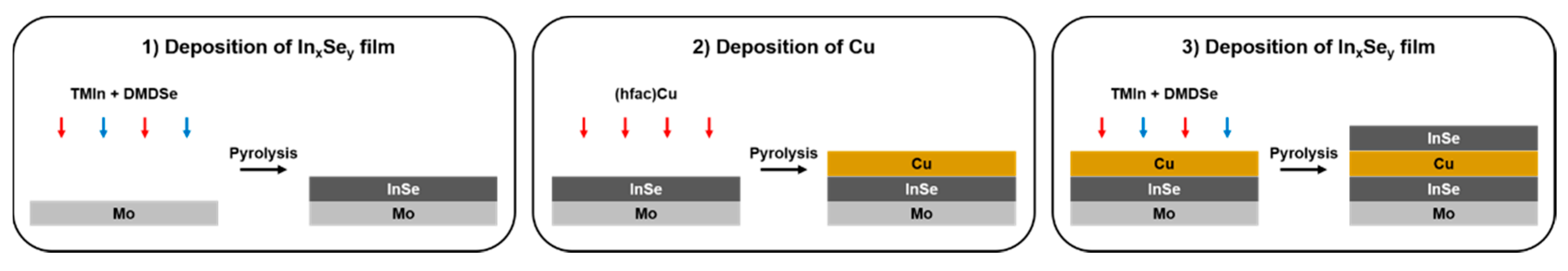
2.1. Fabrication of CIS-Series Solar Cell Samples

Samples of CIS solar cells were prepared via MOCVD as follows. First, a Mo back-contact layer was deposited on a soda-lime glass substrate via MOCVD. As the first step for growing the CIS layer, an InxSey film was deposited with two precursors (TMIn and DMDSe) into a horizontal reactor. Then, Cu was deposited using an (hfac)Cu precursor. As the final step, another InxSey film was deposited using the same precursors (TMIn and DMDSe) (Figure 1). Subsequently, Al-doped ZnO (AZO) was deposited as transparent conductive oxide (TCO) layers via MOCVD. A detailed description of the preparation of the CIGS absorber layer using the three-stage MOCVD process has been provided elsewhere [13].
For a comparative analysis, reference samples were prepared using a three-stage co-evaporation method and two-step solution method. CIGS samples were prepared via three-stage co-evaporation as follows. First, the Mo back-contact layer was deposited on the soda-lime glass substrate through direct-current (DC) magnetron sputtering. Then, CIGS thin films were grown on the Mo-coated soda-lime glass substrates via a three-stage co-evaporation process using four sources—elemental Cu, In, Ga, and Se. In the first stage, In, Ga, and Se were deposited at a low Tsub. of 350 °C to prepare In–Ga–Se precursors. In the second stage, Cu and Se were co-evaporated at 550 °C to grow Cu-rich CIGS thin films. In the third stage, In, Ga, and Se were co-evaporated to complete the growth of Cu-poor CIGS thin films. Devices were fabricated through chemical bath deposition (CBD) of a CdS buffer layer with a thickness of ~60 nm on the as-deposited absorber layers; this was followed by the deposition of intrinsic ZnO (i-ZnO) up to a thickness of 50 nm and AZO up to a thickness of 350 nm using radio frequency (RF) magnetron sputtering. The preparation of the CIGS absorber layer using the three-stage co-evaporation process is described in detail elsewhere [16].
Cu(In,Ga)(S,Se)2 (CIGSSe) samples were prepared using the two-step solution process as follows. First, the Mo back-contact layer was deposited on a soda-lime glass substrate via DC magnetron sputtering. Subsequently, a Cu–In–Ga mixed oxide (CIGOx) layer with a thickness of 1 μm was deposited via iterative spin coating with the alcohol-based precursor solution. This was followed by simultaneous selenization and sulfurization processes. Then, a CdS buffer layer with a thickness of 50 nm was grown on the CIGS layer using CBD, and an i-ZnO layer with a thickness of 50 nm was deposited via RF magnetron sputtering. Finally, AZO was deposited as TCO layers via RF sputtering. The preparation of the CIGS absorber layer using the two-step solution process has been described in detail elsewhere [6].

2.2. Characterization
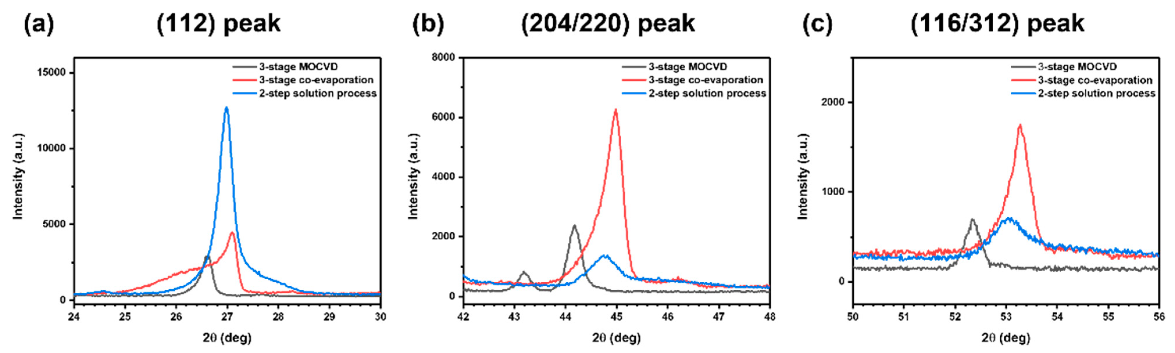
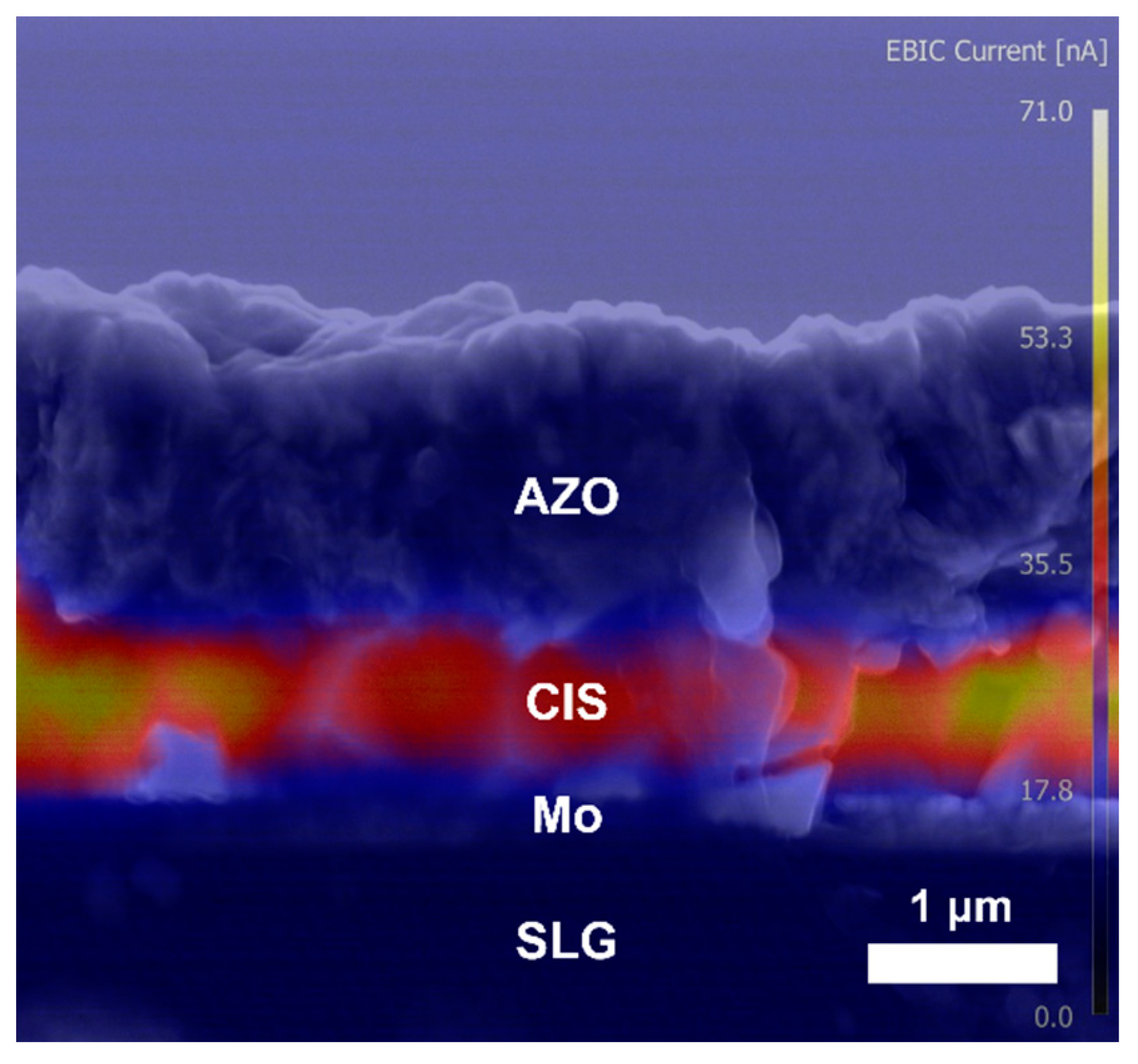
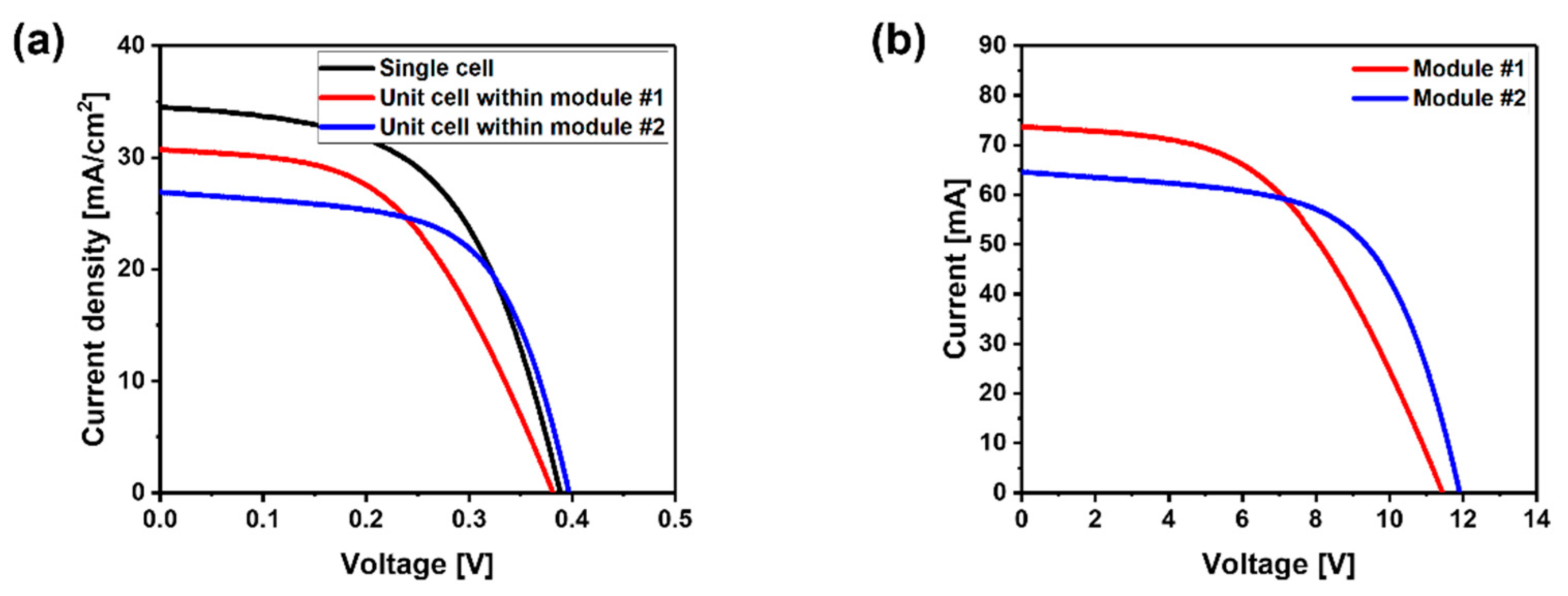
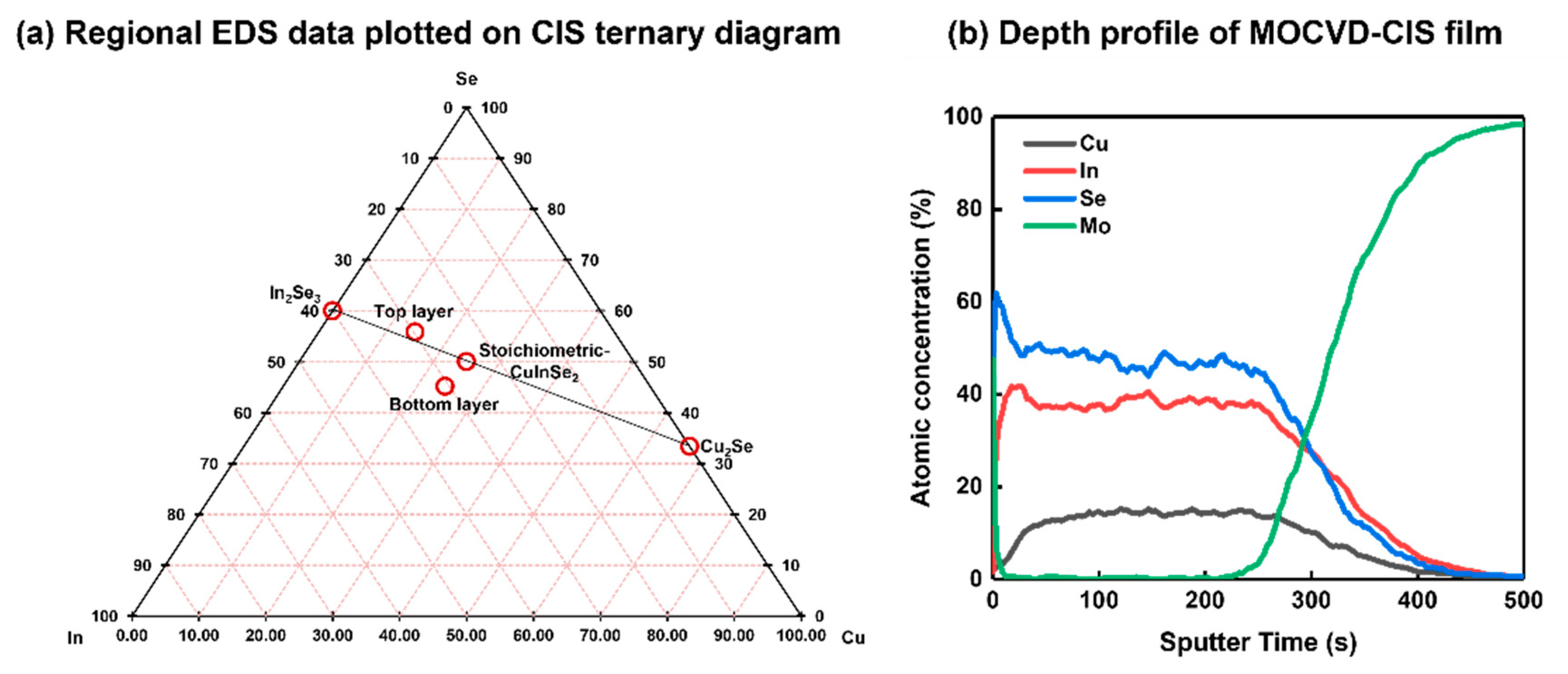
The crystal structure of the CIS films was analyzed using X-ray diffraction (XRD) (Dmax2500/PC). Scanning electron microscopy (SEM) and energy-dispersive X-ray spectroscopy (EDS) (FEI, Inspect F50) were used to investigate the morphologies and element compositions of the films. The depth profiles of the constituents of the film were determined using secondary-ion mass spectrometry (SIMS) (iONTOF, TOF.SIMS5). An electron beam–induced current (EBIC) (FEI, Inspect F) was employed to investigate the junction formation within the films. Finally, the energy-conversion efficiency of the samples was determined by measuring the illuminated I–V characteristics under standard test conditions (WACOM, WXS-156S-10, AM 1.5G).

3. Results

First, we compared the XRD peaks of the MOCVD-prepared CIS sample with those of the CIGS samples prepared using the other deposition techniques, i.e., the three-stage co-evaporation and two-step solution processes [6,17]. Figure 2a–c shows the three main diffraction peaks of the chalcopyrite crystals in the (112), (204/220), and (116/312) planes, respectively [18]. As shown in these figures, the positions of the diffraction peaks of the MOCVD-prepared samples shifted to the left. This occurred because the lattice parameters of the initial chalcopyrite crystal structure vary when different elements, such as Ga and S, are added to the Cu–In–Se ternary system. More specifically, when Ga is added, Ga atoms occupy the initial In atom sites. This, in turn, causes a marginal distortion of the initial crystal structure because of the difference between the radii of the atoms. A similar phenomenon occurs in the cases of S and Se [15]. A simple calculation revealed that a peak shift of approximately 0.5° is reasonable (Table 1). In addition, the XRD data exhibit certain peculiarities. In Figure 2a, a shoulder-shaped two-peak structure is observed for the sample prepared via three-step co-evaporation (red). It has been widely reported that shoulder-shaped XRD spectra appear when Ga has a notch-like distribution within the CIGS layer [19,20,21]. In Figure 2b, for the sample prepared via three-stage MOCVD (black), the peak at approximately 43.2° is ascribed to MOCVD-processed Mo. The use of Mo(CO)6 (a carbonyl group precursor) appears to result in carbon contamination and, thereby, a different crystal structure [22,23,24]. However, it is difficult to distinguish between the α- and β-CIS phases based only on XRD characterization, because these phases are crystallography coherent.
Figure 3a,b show the surface and cross-sectional morphologies, respectively, of the MOCVD-prepared CIS layer, as obtained using SEM. As shown in Figure 3b, the CIS layer was separated into two phases. For a more detailed constituent analysis of each layer, we used both EDS and SIMS characterization. Figure 4a shows a Cu–In–Se ternary diagram with EDS data plotted for the MOCVD-prepared CIS layer. The EDS analysis revealed that the upper layer was a Cu-deficient layer (CDL).
To enhance the credibility of the data, SIMS characterization was also employed. Figure 4b shows the composition depth profile of the MOCVD-prepared CIS layer, which reveals that the upper layer was relatively Cu-poor. This phenomenon occurred because we used a three-stage MOCVD process and because the final layer deposited was the InxSey layer. Here, the process temperature (approximately 320 °C) was lower than that in conventional three-stage co-evaporation (approximately 550 °C) [15]. In general, CDLs are known to be n-type semiconductor materials. An ordered vacancy complex (OVC) is generally used to describe the Cu-deficient phase of CIS. Furthermore, the presence of an OVC generally indicates buried-junction characteristics [25,26,27].
We used EBIC characterization to verify the formation of a buried junction without a buffer layer (Figure 5). Typically, the strongest EBIC signal appears where the electric field is maximized in the EBIC characterization. That is, we can locate the pn junction through EBIC mapping. In a typical CIGS solar cell, the pn junction is near the buffer interface. When a buried junction is formed, the junction position tends to shift toward the bulk [25,26,27]. Accordingly, it can be inferred that the developed device has a buried junction formed by an n-type CDL.
Subsequently, illuminated I–V characteristics were measured to determine whether the sample functioned as an effective photovoltaic device. The cell achieved an energy-conversion efficiency of 7.39%. Although this efficiency is less than that of MOCVD-prepared CIS solar cells (10.45%), the device is effective and requires simpler precursors and processes to manufacture [12]. In particular, our process is feasible for large-scale production since the device achieved an efficiency of approximately 6% at the sub-module scale (Figure 6a,b; Table 2).

4. Conclusions

Previous studies have reported that it is feasible to process chalcopyrite-based photovoltaic devices using the MOCVD technique [9,10,11,12,13,14,15]. However, many previous procedures were too complex for mass production. Therefore, rather than preparing a high-quality single-phase CIS thin film, we created a buried pn junction by utilizing an OVC layer. Consequently, a CIS solar cell with a PCE of 7.39% was developed via a three-stage MOCVD method using (hfac)Cu, TMTIn, and DMDSe precursors. In addition, we fabricated sub-modules to demonstrate that the proposed method is applicable for large-scale production as well.

Author Contributions

Conceptualization, S.H.L.; methodology, S.H.L.; validation, S.H.L. and Y.K.; formal analysis, S.H.L.; investigation, S.H.L.; resources, G.H.L.; data curation, S.H.L.; writing—original draft preparation, S.H.L.; writing—review and editing, S.H.L.; visualization, S.H.L.; supervision, D.K.; project administration, H.-S.L.; funding acquisition, H.-S.L. All authors have read and agreed to the published version of the manuscript.

Funding

This work was supported by the “Human Resources Program in Energy Technology” of the Korea Institute of Energy Technology Evaluation and Planning (KETEP), and granted financial resources from the Ministry of Trade, Industry & Energy, Republic of Korea (No. 20204010600470). This work was also supported by the KU-KIST Graduate School Project.

Institutional Review Board Statement

Not applicable.

Informed Consent Statement

Not applicable.

Data Availability Statement

Not applicable.

Conflicts of Interest

The authors declare no conflict of interest.

References

  1. Green, M.; Dunlop, E.; Hohl-Ebinger, J.; Yoshita, M.; Kopidakis, N.; Hao, X. Solar cell efficiency tables (version 57). Prog. Photovolt. Res. Appl. 2021, 29, 3–15. [Google Scholar] [CrossRef]
  2. Li, R.; Liu, M.; Matta, S.K.; Hiltunen, A.; Deng, Z.; Wang, C.; Dai, Z.; Russo, S.P.; Vivo, P.; Zhang, H. Sulfonated dopant-free hole-transport material promotes interfacial charge transfer dynamics for highly stable perovskite solar cells. Adv. Sustain. Syst. 2021, 2100244. [Google Scholar] [CrossRef]
  3. Zhang, H.; Liu, M.; Yang, W.; Judin, L.; Hukka, T.I.; Priimagi, A.; Deng, Z.; Vivo, P. Thionation enhances the performance of polymeric dopant-free hole-transporting materials for perovskite solar cells. Adv. Mater. Interfaces 2019, 6, 1901036. [Google Scholar] [CrossRef]
  4. Mitchell, V.D.; Jones, D.J. Advances toward the effective use of block copolymers as organic photovoltaic active layers. Polym. Chem. 2018, 9, 795–814. [Google Scholar] [CrossRef]
  5. Zhan, X.; Zhu, D. Conjugated polymers for high-efficiency organic photovoltaics. Polym. Chem. 2010, 1, 409–419. [Google Scholar] [CrossRef]
  6. Lee, S.H.; Kim, M.K.; Bae, S.; Nam, J.; Park, H.; Lee, S.W.; Jang, Y.J.; Min, B.K.; Yang, J.Y.; Kang, Y.; et al. Absorber delamination-induced shunt defects in alcohol-based solution-processed Cu(In,Ga)(S,Se)2 solar modules. ACS Appl. Energy Mater. 2020, 3, 10384–10392. [Google Scholar] [CrossRef]
  7. Irvine, S.J.C.; Barrioz, V.; Lamb, D.; Jones, E.W.; Rowlands-Jones, R.L. MOCVD of thin film photovoltaic solar cells—Next-generation production technology? J. Cryst. Growth 2008, 310, 5198–5203. [Google Scholar] [CrossRef]
  8. Niki, S.; Contreras, M.; Repins, I.; Powalla, M.; Kushiya, K.; Ishizuka, S.; Matsubara, K. CIGS absorbers and processes. Prog. Photovolt. Res. Appl. 2010, 18, 453–466. [Google Scholar] [CrossRef]
  9. Thompson, A.G. MOCVD technology for semiconductors. Mater. Lett. 1997, 30, 255–263. [Google Scholar] [CrossRef]
  10. Mufti, N.; Amrillah, T.; Taufiq, A.; Diantoro, M.; Nur, H. Review of CIGS-based solar cells manufacturing by structural engineering. Sol. Energy 2020, 207, 1146–1157. [Google Scholar] [CrossRef]
  11. Sagnes, B.; Salesse, A.; Artaud, M.C.; Duchemin, S.; Bougnot, J.; Bougnot, G. MOCVD growth of CuInSe2: First results. J. Cryst. Growth 1992, 124, 620–627. [Google Scholar] [CrossRef]
  12. Artaud, M.C.; Ouchen, F.; Martin, L.; Duchemin, S. CuInSe2 thin films grown by MOCVD: Characterization, first devices. Thin Solid Films 1998, 324, 115–123. [Google Scholar] [CrossRef]
  13. Choi, I.H. The preparation of a CuInSe2 solar cell by metal organic chemical vapor deposition. Thin Solid Films 2012, 525, 137–140. [Google Scholar] [CrossRef]
  14. Cho, J.Y.; Jeong, H.C.; Kim, K.S.; Kang, D.H.; Kim, H.K.; Shim, I.W. Preparation of phase-pure InSe thin films by MOCVD using a new single-source precursor [(Me)2In(μ-SeMe)]2. Bull. Korean Chem. Soc. 2003, 24, 645–646. [Google Scholar]
  15. Choi, I.H.; Lee, D.H. Preparation of CuIn1−xGaxSe2 films by metalorganic chemical vapor deposition using three precursors. Thin Solid Films 2007, 515, 4778–4782. [Google Scholar] [CrossRef]
  16. Gwak, J.; Lee, M.; Yun, J.H.; Ahn, S.; Cho, A.; Ahn, S.; Humle, J.P.; Shin, K.E.; Yoon, K.H. Selenium flux effect on Cu(In,Ga)Se2 thin films grown by a 3-stage co-evaporation process. Isr. J. Chem. 2015, 55, 1115–1122. [Google Scholar] [CrossRef]
  17. Luque, A.; Hegedus, S. (Eds.) Handbook of Photovoltaic Science and Engineering; John Wiley & Sons, Ltd.: Chichester, UK, 2011. [Google Scholar]
  18. Delgado, G.E.; Manfredy, L.; López-Rivera, S.A. Crystal structure of the ternary semiconductor Cu2In14/3 4/3Se8 determined by X-ray powder diffraction data. Powder Diffr. 2018, 33, 237–241. [Google Scholar] [CrossRef]
  19. Liang, X.; Zhu, H.; Chen, J.; Zhou, D.; Zhang, C.; Guo, Y.; Niu, X.; Li, Z.; Mai, Y. Substrate temperature optimization for Cu(In,Ga)Se2 solar cells on flexible stainless steels. Appl. Surf. Sci. 2016, 368, 464–469. [Google Scholar] [CrossRef]
  20. Klinkert, T.; Jubault, M.; Donsanti, F.; Lincot, D.; Guillemoles, J.F. Ga gradients in Cu(In,Ga)Se2: Formation, characterization, and consequences. J. Renew. Sustain. Energy 2014, 6, 011403. [Google Scholar] [CrossRef]
  21. Zhang, W.; Zhu, H.; Zhang, L.; Guo, Y.; Niu, X.; Li, Z.; Chen, J.; Liu, Q.; Mai, Y. Cu(In,Ga)Se2 thin film solar cells grown at low temperatures. Solid State Electron. 2017, 132, 57–63. [Google Scholar] [CrossRef]
  22. Wei, W.C.J.; Lo, M.H. Processing and properties of (Mo, Cr) oxycarbides from MOCVD. Appl. Organomet. Chem. 1998, 12, 201–220. [Google Scholar] [CrossRef]
  23. Djajanti, S.D.; Howe, R.F. MOCVD in zeolites using Mo(CO)6 and W(CO)6 as precursors. In Studies in Surface Science and Catalysis; Elsevier: Amsterdam, The Netherlands, 1995; pp. 197–204. [Google Scholar]
  24. Schaefer, C.M.; Caicedo Roque, J.M.; Sauthier, G.; Bousquet, J.; Hébert, C.; Sperling, J.R.; Pérez-Tomás, A.; Santiso, J.; del Corro, E.; Garrido, J.A. Carbon incorporation in MOCVD of MoS2 thin films grown from an organosulfide precursor. Chem. Mater. 2021, 33, 4474–4487. [Google Scholar] [CrossRef]
  25. Ishizuka, S.; Yamada, A.; Fons, P.J.; Kamikawa-Shimizu, Y.; Komaki, H.; Shibata, H.; Niki, S. Buried pn junction formation in CuGaSe2 thin-film solar cells. Appl. Phys. Lett. 2014, 104, 031606. [Google Scholar] [CrossRef]
  26. Schmid, D.; Ruckh, M.; Grunwald, F.; Schock, H.W. Chalcopyrite/defect chalcopyrite heterojunctions on the basis of CuInSe2. J. Appl. Phys. 1993, 73, 2902–2909. [Google Scholar] [CrossRef]
  27. Zhao, Y.; Yuan, S.; Chang, Q.; Zhou, Z.; Kou, D.; Zhou, W.; Qi, Y.; Wu, S. Controllable formation of ordered vacancy compound for high efficiency solution processed Cu(In,Ga)Se2 solar cells. Adv. Funct. Mater. 2021, 31, 2007928. [Google Scholar] [CrossRef]
Figure 1. Schematic of the three-step MOCVD process for CIS layer deposition.
Energies 14 07721 g001
Figure 2. Three main XRD peaks of chalcopyrite crystal structure: (a) (112) peak; (b) (204/220) peak; (c) (116/312) peak.
Energies 14 07721 g002
Figure 3. Morphology of MOCVD-prepared CIS layer: (a) SEM top-view image; (b) SEM cross-sectional image.
Energies 14 07721 g003
Figure 4. Comparative constituent analysis of the top and bottom layers using (a) EDS and (b) SIMS.
Energies 14 07721 g004
Figure 5. EBIC mapping image of MOCVD-prepared buffer-less CIS solar cell.
Energies 14 07721 g005
Figure 6. Illuminated I–V characteristics of an MOCVD-prepared CIS solar cell under standard test conditions (STC, 100 mW cm−2). (a) J–V characteristics of a cell and calculated J–V characteristics of sub-modules #1 and #2. (b) I–V characteristics of sub-modules #1 and #2.
Energies 14 07721 g006
Table 1. Diffraction-peak positions of various types of chalcopyrite structure samples.
Crystallographic PlanesDiffraction Peak Positions (2θ)
MOCVD-Processed CISCo-Evaporation-Processed CIGSSolution-Processed CIGSSe
(112)26.62°27.10°26.98°
(204/220)44.18°44.98°44.74°
(116/312)52.34°53.28°53.04°
Table 2. Photovoltaic performance of an MOCVD-prepared CIS solar cell and sub-modules.
SampleSingle CellModule #1Module #2
VOC [V]0.3870.3810.397
JSC [mA/cm2]34.530.726.9
Fill factor [%]55.450.361.6
Series resistance [Ω cm2]2.5424.2262.353
Series resistance [Ω cm2]175.1192.1148.3
Efficiency [%]7.395.886.57
Area0.5 × 0.5 cm8 × 9 cm
(with 30-unit cells)
8 × 9 cm
(with 30-unit cells)
Publisher’s Note: MDPI stays neutral with regard to jurisdictional claims in published maps and institutional affiliations.

