Article

Design of a Highly Efficient N-Stage Harmonic Terminated Voltage Multiplier for Wireless Power Transfer

Department of Electronics and Communication, Konkuk University, Seoul 05029, Korea
*
Author to whom correspondence should be addressed.
Energies 2021, 14(21), 7203; https://doi.org/10.3390/en14217203
Submission received: 30 August 2021 / Revised: 14 October 2021 / Accepted: 15 October 2021 / Published: 2 November 2021

Abstract

:
This paper proposes a 5.8 GHz highly efficient rectifier design using harmonic termination for wireless power transfer. The diode used to convert the received RF power to DC is a non-linear device, and a harmonic component is generated, which causes performance degradation. Therefore, in this paper, we designed a band stop filter for harmonic termination and proposed the N-stage harmonic terminated voltage multiplier (N-stage HTVM). The number of stages N can be designed differently to operate with high efficiency at various input powers for the proposed rectifier. In the proposed rectifier circuit, mathematical analysis of output DC voltage, power loss of the diode, and the power conversion efficiency (PCE) were evaluated through voltage/current waveform analysis of the diode. The design method of the filter for terminating harmonics is presented. Furthermore, the change of PCE according to the increase in the number of stages was analyzed using the equivalent model of the proposed circuit and verified through measurement. The maximum PCE of one-stage HTVM was 68% when 18 dBm of input power was applied. The DC output voltage was measured to 11.6 V. When the RF input power was 25 dBm and the load was 1500 Ω , the maximum PCE of the two-stage HTVM was 71% and the maximum DC output voltage was measured as 15.8 V. The measured performance of three-stage HTVM had a PCE of 67% and DC output voltage of 19.8 V when the input power was 30 dBm.

1. Introduction

Microwave wireless power transfer (MRWPT) is being actively studied as a technology for wireless charging in various environments, such as artificial satellites, medical devices, and smart offices. MRWPT is a method of radiating generated microwave power to phased array antennas and supplying power through an electromagnetic field. MRWPT can transmit a longer distance than magnetic resonant WPT, but the power transfer efficiency (PTE) decreases as the transmitter (TX) and receiver (RX) distance increases. The performance of the MRWPT is determined not only by the PTE but also by the power amplifier (PA), phased array antenna (PAA), beamforming algorithm and receiver performance [1].
The RX for MRWPT is used not only for WPT but also for energy harvesting. It consists of an array receiving antenna, the impedance matching unit, the rectifier, and a load. The part that determines the performance of the receiver is the rectifier. There are various rectifier design methods [1,2,3,4,5,6]. A half-wave rectifier circuit [1,2] can convert the input signal in the positive or negative region to DC by arranging Schottky diodes in series or shunts. A series of diode rectifiers was proposed, and a dual-band rectenna at 2.4 and 5.8 GHz was designed [1].
The power conversion efficiency (PCE) of the rectifier is 63% at 2.4 GHz and 54.8% at 5.8 GHz at an input power of 10 mW. A shunt diode rectifier using load-pull [2] has PCE of 63% at an input power of 10 dBm. Although the shunt diode rectifier requires low design difficulty with simple structure, it has low rectification efficiency and a very high impedance of the load. A full-wave rectifier circuit, which converts the entire input signal to DC using two or four Schottky diodes, with harmonic termination of 5.8 GHz signal has PCE of 65.3% at 15 dBm [3]. It has higher rectification efficiency than a half-wave rectifier circuit [1].
However, its structure is complicated. A Class C single Schottky diode rectifier and Class F 1 GaN transistor rectifier based on the power amplifier theory was also proposed [4]. A Class C rectifier operating at a 2.45 GHz band uses a shunt diode shorted to the second and third harmonics. It has a PCE of 72% at an input power of 7 dBm [4]. A Class F rectifier using even order harmonic control with shorted stubs and odd order harmonic control with open stubs has been proposed [5]. When operating at 5.81 GHz, it has a PCE of 69.2% using series diode and harmonic cancellation at an input power of 8.2 dBm [5]. A Class F rectifier using Dickson charge pump in 5.2 GHz band has a PCE of 64% at an input power of 23 dBm [6].
As mentioned above, there have been studies on the design of rectifiers using various topologies. However, Refs. [5,6] targeted systems that convert relatively low RF power into DC, such as energy harvesting and Internet of Things (IoT) sensor driving. However, the power density delivered to the receiver varies depending on the surrounding environment and location. In the wireless power transfer environment, the received power density changes due to the distance of the transmitting/receiving antenna, beamforming performance, etc., in particular.
Existing topologies [5,6] are challenging to apply to a wireless power transfer system to which a high power density is used due to the performance limitations of diodes. Therefore, it is necessary to design a rectifier with high PCE according to various input powers. This paper proposes a rectifier design that shows PCE when high power density is applied in various wireless power transfer environments.
Ref. [7] proposed a rectenna design that exhibits more than 50% PCE in a wide range of input power (−10∼25 dBm) in a wireless power transfer system. Ref. [7] designed an impedance matching unit according to low power density and high power density and showed a maximum PCE performance of 70.2% at an input power of 17 dBm. Ref. [8] proposed array rectifiers with an adaptive power distribution network (APDN). APDN consists of a rectifier cell for high frequency and high power and a rectifier cell for low frequency and low power intensity.
Ref. [9] designed a rectenna showing high PCE (86%) performance at high input power (27 dBm) in a scenario where multi-tone (1.7 GHz and 2.4 GHz) is applied to the receiver. Ref. [10] proposed a rectifier designed to operate in various frequency ranges by using harmonic termination when a two-tone or four-tone signal is applied to the receiver.
Ref. [11] proposed a power recycling network (PRN) during a study to receive a wide input power range in a wireless power transmission environment and showed more than 50% PCE performance in the input power range of 10.5∼31.8 dBm. The PRN consists of two rectifier cells, and unlike [8], an impedance matching unit was designed so that the reflected power can be applied to other rectifier cells.
Ref. [12] proposed a structure of two rectifier cells like [8,11], and, to compensate for the reflected power, a hybrid coupler and a phase shift unit were implemented. The rectifier circuit proposed in [12] showed more than 50% of PCE performance even when the size range of the load (8 to 97 k Ω ) was wide. The diodes used in studies covering the low input power range to the wide input power range were mainly Schottky diodes. Ref. [13] proposed a wire-bonded GaN diode rectifier to show high performance at high input power.
As above, existing studies have proposed a rectifier operating at relatively low power and high load impedance [1,2,3,4,5,6], or a receiver operating over a wide input power range in a changing wireless power transfer environment [7,8,9,10,11,12]. Alternatively, a rectifier using a GaN device for high input power has been proposed. GaN diodes exhibit higher breakdown voltage characteristics than Schottky diodes made of silicon, and thus they are suitable for high input power devices. The design difficulty of GaN diodes in the C-Band (4∼8 GHz) or higher band is very difficult, and the manufacturing cost is high.
However, to sufficiently supply power to devices, such as sensors and smartphones through PAA beamforming, it is necessary to design and mathematically analyze a rectifier with high PCE performance at high input power. Since a diode or transistor, which is a core element of a rectifier, is a nonlinear element, it is essential to design it through a nonlinear analysis and a behavioral model [14,15]. In addition, a diode must be selected according to the input power level, and a rectifier was designed based on the electrical characteristics of the adopted diode.
In this paper, we propose a method to derive the output voltage, current, and power loss of the rectifier to be designed using a nonlinear mathematical approach based on the electrical characteristics of the diode. Therefore, the proposed method was analyzed using the voltage and current waveforms of diodes, and a harmonic termination filter was designed to improve switching efficiency. Finally, an N-stage harmonic terminated voltage multiplier (N-stage HTVM) was designed. The proposed N-stage HTVM was analyzed with mathematical analysis of the diode waveform and power loss of the diode.
This paper is prepared with the following structure. First, the mathematical analysis of the proposed rectifier is shown in Section 2. Section 3 describes the design process of the harmonic termination filter. The performance of the N-stage HTVM is validated by simulation and measurement in Section 4, and our conclusions are made in Section 5.

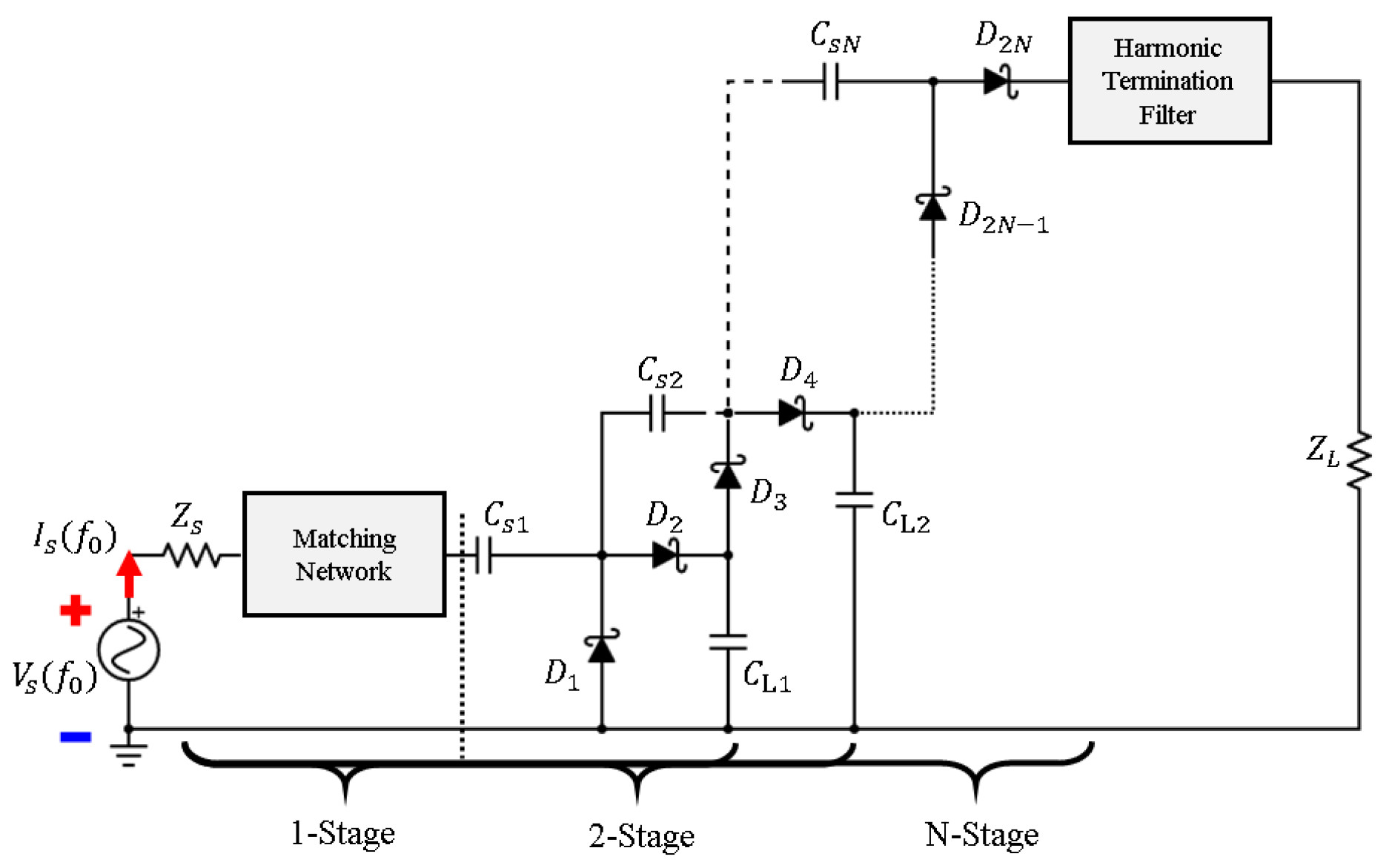
2. N-Stage Harmonic Terminated Voltage Multiplier Theory

A one-stage voltage multiplier (VM) consists of two diodes and two capacitors with DC voltage twice the input voltage as output. However, the output voltage decreases due to the built-in potential (threshold voltage) the loss caused by parasitic components and junction capacitors. Therefore, the N-stage VM is composed of diodes and capacitors with a DC voltage of less than the input voltage as output.
Figure 1 shows the circuit diagram of N-stage HTVM. A harmonic terminated rectifier, like Class F or Class F 1 , has different performances depending on which diode the filter is positioned. The design method of the filter is also different. In this paper, if there are diodes, the harmonic termination filter is placed behind the diode. Impedance characteristics of the harmonic termination filter applied in the proposed rectifier show that the impedance of the even order term is short, and the impedance of the odd order term is open, like a Class F rectifier.

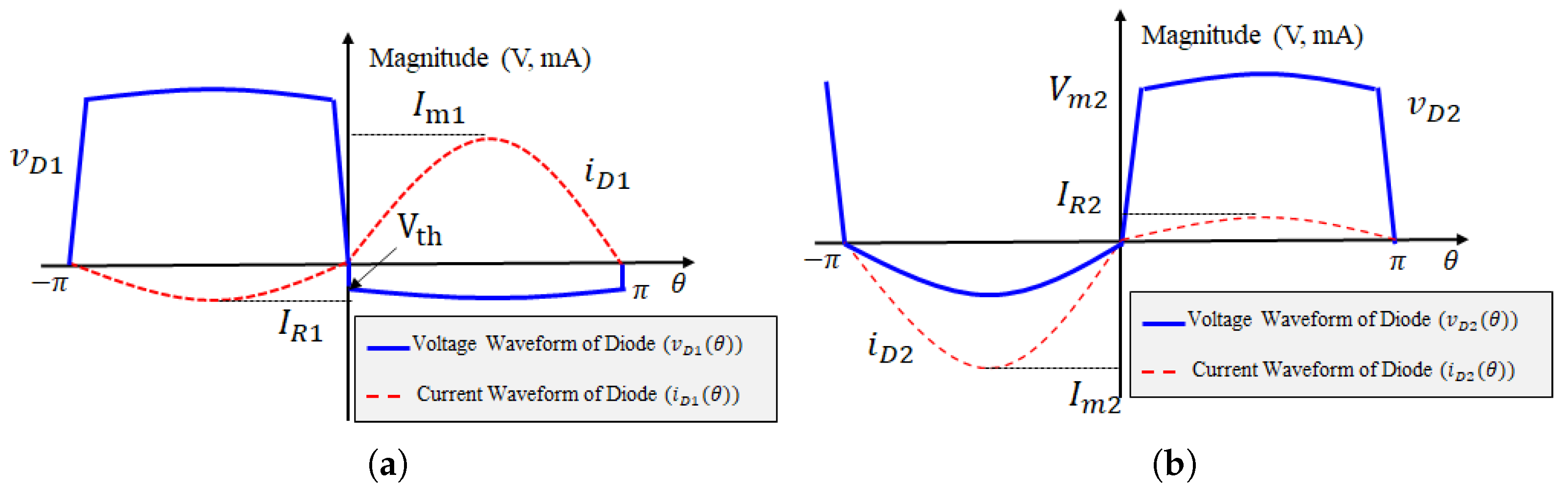
2.1. Mathematical Analysis of N-Stage HTVM under Breakdown Voltage Region

If characteristics of the harmonic termination filter show that the impedance of even order is short and that of odd order is open and that the filter is located behind the diodes arranged in series shown in Figure 2a. The voltage and current waveforms of the diode connected to the shunt will appear as sine waves, respectively, as shown in Figure 2b.
The voltage waveform of the diode will appear as a square wave as shown in Figure 2c in the low input power region and the current waveform will appear as a sine wave when the voltage is 0. The voltage will appear as a non-zero value in the section due to the built-in potential. However, as shown in Figure 2, the diode voltage and current waveforms are satisfied in the low power region when the input power before the breakdown voltage of the diode is applied.
In Figure 2a, C s is the charging capacitor for boosting voltage, v s is the source voltage, Z s is the source impedance, v D 1 and v D 2 are the voltages across diodes D 1 and D 2 , C L is the equalization capacitor, Z L is the load impedance, where V D C is output DC voltage, and V m 1 and V m 2 are the maximum magnitude of v D 1 and v D 2 . I m 1 and I m 2 are the maximum magnitudes of i D 1 and i D 2 where current is flowing through D 1 and D 2 . R s is the parasitic resistance in the diode. The voltage and current in Figure 2b are expressed as Equations (1) and (2) as shown in Figure 2c.
v D 1 θ = V m 1 sin θ π < θ < 0 V t h 0 < θ < π i D 1 θ = 0 π < θ < 0 I m 1 sin θ 0 < θ < π
v D 2 θ = V t h + I m 2 R s sin θ π < θ < 0 V m 2 0 < θ < π i D 2 θ = I m 2 sin θ π < θ < 0 0 0 < θ < π
DC components ( V 01 and V 02 ) of the voltage across D 1 and D 2 during one cycle, can be expressed as Equations (3) and (4).
V 01 = 1 2 π π π v D 1 d θ = 2 V m 1 π V t h 2 π
V 02 = 1 2 π π π v D 2 d θ = 2 I m 2 R s π V t h + V m 2 2 π
where V t h is the built-in potential of the diode. V D C across the load can be expressed as Equation (5) where N is the number of stages (consisting of one shunt diode and one series diode):
V D C N = N V 01 + V 02 = N 2 V m 1 + V m 2 2 π V t h 2 I m 2 R s 2 π
where ω is the angular frequency. Since the output voltage is calculated, the DC output power P o u t = V D C I D C = V D C 2 / Z L is defined, and PCE η is defined as Equation (6):
η = P o u t P o u t + P l o s s
P l o s s consists of a loss due to the built-in potential of the diode and the junction capacitor. Losses like these can cause an overlap section between the voltage and current waveforms of the diode. In Figure 2c, overlap sections of v D 2 , i D 2 are defined as Equation (7). In the case of D 1 , the power loss is zero since there is no overlapping section.
P l o s s , V t h = 1 2 π π 0 v D 1 i D 1 d θ = I m 2 I m 2 R s π + 4 V t h 4 π
A junction capacitor C j exists inside the diode. This component generates a rising edge loss and a falling edge loss when the diode is turned on and off. The rising edge and falling edge are factors that cause voltage and current waveforms to overlap with each other and lead to a loss. These losses can be calculated with Equations (8)–(10), where f is the operating frequency and δ is the Dirac delta function [16]. The magnitude of the rising edge loss and falling edge loss is proportional to the magnitude and frequency of the junction capacitor. Since the voltage waveform of D 1 is not dynamically switched, losses caused by the junction capacitor are neglected.
v D 2 t = 0 = 1 2 v D 2 t = 0 + + v D 2 t = 0 = V m 2 2
i D 2 t = 0 = C j d v D 2 d t t = 0 = C j v m 2 δ ( t 0 )
P l o s s , C j = 1 2 π π π v D 2 t = 0 i D 2 t = 0 d θ = 1 2 f C j V m 2 2
If Equations (7) and (10) are arranged with the number of stages, the following is obtained:
P l o s s ( N ) = N ( P l o s s , V t h + P l o s s , C j ) = N 2 π V m 2 2 f C j + I m 2 ( I m 2 R S π + 4 V t h ) 4 π
By substituting Equations (5) and (11) of V D C and P l o s s into Equation (6), PCE under breakdown voltage η 1 is arranged as follows, where B = 2 V m 1 + V m 2 2 π V t h 2 I m 2 R S
η 1 = V D C 2 V D C 2 + Z L P l o s s = N B 2 N B 2 + π Z L 2 π V m 2 2 f C j + I m 2 I m 2 R S π + 4 V t h

2.2. Mathematical Analysis of N-Stage HTVM over Breakdown Voltage Region

In a diode, the current flows in a forward direction. No current flows in the reverse direction. However, if the reverse voltage is continuously raised, a current can suddenly flow at any moment. The voltage at this time is called the breakdown voltage. When a voltage greater than the breakdown voltage is applied to the diode in the reverse direction, leakage current will flow, which is the main cause of degradation of the diode parameters.
When the region above the breakdown voltage is referred to as the high power region, the voltage and current waveforms of the diode overlap each other more than the low power region and appear, including a leakage current. Figure 3 shows the voltage and current waveforms of D 1 and D 2 over the breakdown voltage region.
Assuming that the voltage and current of the diode for one cycle in the high power region are v D 1 b r , v D 2 b r , i D 1 b r , and i D 2 b r , the following equations are given.
v D 1 _ b r θ = V b r + I R 1 R s sin θ π < θ < 0 V t h + I m 1 R s sin θ 0 < θ < π i D 1 _ b r θ = I R 1 sin θ π < θ < 0 I m 1 sin θ 0 < θ < π
v D 2 _ b r θ = V t h + I m 2 R s sin θ π < θ < 0 V b r + I R 2 R s sin θ 0 < θ < π i D 2 _ b r θ = I m 2 sin θ π < θ < 0 I R 2 sin θ 0 < θ < π
where V b r is the breakdown voltage, I m 1 and I m 2 are the maximum magnitudes of forward current, and I R 1 and I R 2 are the maximum magnitude of the reverse current. The DC voltage component V 01 _ b r and V 02 _ b r and power loss P l o s s _ b r can be obtained from the voltage and current waveform of the diode defined above.
V 01 _ b r = 1 2 π π π v D 1 _ b r d θ = π V b r π V t h + 2 I m 1 R S 2 I R 1 R S 2 π
V 02 _ b r = 1 2 π π π v D 2 _ b r d θ = 2 I m 2 R S + 2 I R 2 R S π V t h + π V b r 2 π
Power losses on the junction capacitance at the two transition periods are zero since the losses at the rising and falling edges will cancel out each other. The power loss on R s due to the current induced by C j can be calculated as follows:
P l o s s , C j _ b r = 1 2 π 0 τ π C j d V D 2 d θ d θ d t 2 R S d θ + 1 2 π ( 1 τ ) π π C j d V D 2 d θ d θ d t 2 R S d θ = 4 f 2 C j 2 V b r 2 R S τ
where τ is the ratio of rising and falling time with respect to half the period assumed. The loss due to V t h can be calculated by integrating the instantaneous voltage and current across the diode during one period as follows:
P l o s s , V t h _ b r = 1 2 π π π v D 1 _ b r i D 1 _ b r + 1 2 π π π v D 2 _ b r i D 2 _ b r = π I m 2 2 R S + π I R 2 2 R S + 4 I m 2 V t h + 4 I R 2 V b r 2 π
Therefore, the voltage applied to the load in the high power region of the N-stage HTVM is as follows:
V D C _ b r N = N V 01 _ b r + V 02 _ b r = N V b r V t h + N R S I m 1 I m 2 + I R 2 I R 1 π
The loss occurring in the diode in the high power region can be expressed as the sum of the loss due to C j and V t h as in Equation (11). Losses increase as the number of stages increases. Finally, the PCE over breakdown voltage is as follows, where A = 8 π f 2 C j 2 V b r 2 R S + τ π I m 2 2 R S + π I R 2 2 R S + 4 I m 2 V t h + 4 I R 2 V b r .
η 2 = P o u t _ b r P o u t _ b r + P l o s s _ b r = V D C _ b r N 2 V D C _ b r N 2 + Z L P l o s s _ b r N = 2 N π V b r V t h + R S I m 1 I m 2 + I R 2 I R 1 2 2 N π V b r V t h + R S I m 1 I m 2 + I R 2 I R 1 2 + Z L π A
Diode parameters C j , R s , V t h , and V b r and rectifier parameters Z L , N, P i n , f, and τ are known variables that can be easily obtained. By calculating Equation (20), the efficiency of N-stage HTVM ( η 2 ) in the high input power region can be obtained. By calculating Equation (14), the efficiency of N-Stage HTVM ( η is the sum of results of η 1 and η 2 intervals) in the low power region can be obtained. By dividing η 1 and η 2 based on V b r , the PCE for the input power of N-Stage HTVM can be calculated. A termination filter design is required to form the diode’s voltage and current waveforms as above. The filter design is described in the next chapter.

3. Design Method of Harmonic Termination Filter

The harmonic termination (HT) filter can be designed through the transmission line theory. A HT filter is mainly designed to pass and block with an input impedance determined by the electrical length of the open-ended stub and short stub. There are various other HT filter design methods. In this paper, only open-ended stubs are used and designed as shown in Figure 4. The filter is designed using only open stubs because it is easy to design. In addition, characteristics do not change dramatically even when the deformed form is the same as the bent form. Thus, it is suitable for miniaturization and tuning.
The third harmonic term appears to be short in the admittance characteristic seen from the input terminal of the open-ended stub having an electrical length of λ / 12 . However, its impedance characteristic, which is the reciprocal of it, appears to be open. Therefore, the impedance characteristics of harmonic components seen from the input Z λ / 12 can be expressed as follows:
Z λ / 12 ( ω ) = j Z 01 cot π 6 ω ω 0 = ω = 0 1.73 j Z 01 ω = ω 0 0.57 j Z 01 ω = 2 ω 0 0 ω = 3 ω 0
where Z 01 is the characteristic impedance of λ / 12 electrical length open-ended stub, and ω is the fundamental angular frequency. As for the input admittance characteristics of an open-ended stub having an electrical length of λ / 4 , the second harmonic term appears to be open, and the third harmonic term appears to be short. However, since the impedance characteristic seen from the input terminal has an inverse relationship, the second harmonic term seems to be short, and the third harmonic term appears to be open, which can be expressed as the following equation:
Z λ / 4 ( ω ) = j Z 01 cot π 6 ω ω 0 = ω = 0 0 ω = ω 0 ω = 2 ω 0 0 ω = 3 ω 0
where Z 02 is the characteristic impedance of λ / 4 electrical length open-ended stub. The HT filter was designed with impedance characteristics obtained from Equations (21) and (22). The sum of electrical lengths of transmission lines between each stub is λ / 2 . Furthermore, if double open-ended stubs are configured, the characteristic impedance is reduced. Thus, the bandwidth increases, rather than composing an HT filter with one open-ended stub, as shown in Figure 4. Figure 5 shows input impedance and E-field through EM simulation of the designed filter.
When the center frequency of the HT filter designed in Figure 5 is 5.8 GHz, odd harmonic terms (5.8 and 17.4 GHz) seems to be open, while even harmonic term (11.6 GHz) seems to be short. EM simulation confirmed that the desired frequency characteristics were obtained from the E-field distribution.

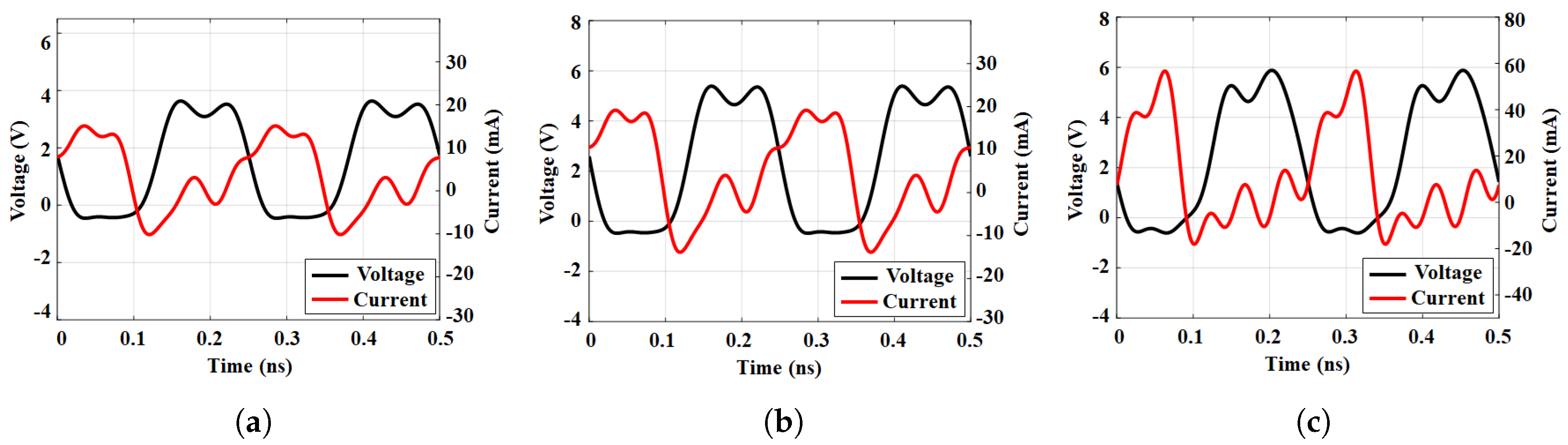
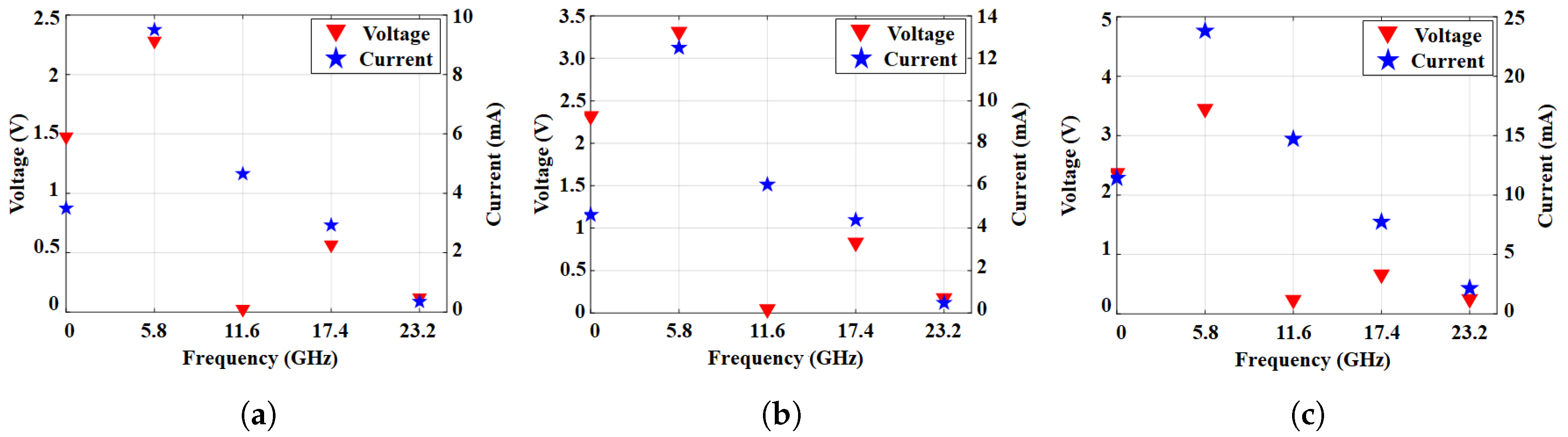
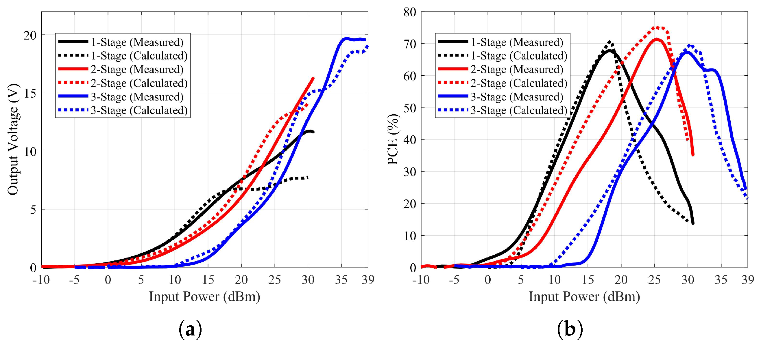
4. Simulation and Measurement

The performance of N-stage HTVM was determined through model verification and circuit simulation based on measurement results. Table 1 shows the parameters used for model verification and circuit simulation.
Figure 6 shows diode voltage and current waveforms in the time domain, and Figure 7 shows harmonics in the frequency domain when the number of stages is 1–3. One of the reasons for the difference between Figure 2, Figure 3 and Figure 6 is that C j and R s have different sizes. As C j and R s are smaller, the voltage waveform of the diode appears ideally. Figure 6 shows a simulation using the actual diode parameters shown in Table 1.
As the number of stages increases, the voltage across the diode increases. According to the impedance characteristics of the HT filter, the voltage waveform of the diode appears as a square wave, and the third harmonic term seems to be higher than the even-order term as shown in Figure 7.
To verify the model proposed in Figure 8, circuit simulation results were compared. The red dotted line shows the model composed of V D C and V D C _ b r according to the input power, and the black solid line shows results of the Microwave Office (MWO) simulator. Figure 9 shows the measurement setup and the fabricated PCB to measure the performance of the N-stage HTVM. NI Universal Software Radio Peripheral (USRP B210) was used to generate RF signal at 5.8 GHz, and Qorvo’s QPA9501 PA was used to apply RF power of 10 dBm or more. The amplitude of the USRP input signal was swept using Labview software and applied to the proposed rectifier up to 39 dBm, the maximum output power of PA.
To monitor the input power applied to the rectifier, a 34.5 dB bi-directional coupler from Mini-Circuits was used and the reflected power was also observed. An Anritsu MS2713E spectrum analyzer was used to monitor the RF Power. Finally, to measure the DC output voltage and current of the rectifier according to the size of the load, a Keithley’s 2380-120-60 DC electronic load was used. Figure 10 shows the measured and calculated output voltages and PCEs according to the input power for a 1500 Ω load. The black and red solid lines indicate the measured output voltage and the calculated output voltage, respectively. The black dotted line and red dotted line show the measured PCE and the calculated PCE, respectively.
The results of Figure 10 are summarized in Table 2. Table 3 shows the performance of the rectifier proposed in this paper compared with previous studies.

5. Conclusions

In this paper, we proposed an N-stage HTVM with a designed harmonic termination filter. When a HT filter was applied, the DC component and loss were calculated based on the voltage and current waveforms of the diode. Finally, the PCE was derived. The proposed model was verified by comparing the circuit simulation and measurement results. The voltage and current waveforms of the diode were analyzed according to the number of stages.
When the operating frequency was 5.8 GHz, the load impedance was 1500 Ω , and the input power was 18 dBm, the maximum output voltage of one-stage HTVM was 11.6 V, and the maximum PCE was 68%. When the load impedance was 1500 Ω and the input power was 25 dBm, the maximum output voltage of the two-stage HTVM was 15.8 V, and the maximum PCE was 71%. Finally, when the load impedance was 1500 Ω and the input power was 30 dBm, the maximum output voltage of the three-stage HTVM was 19.8 V and the maximum PCE was 67%.
Experiments and model verification confirmed that the input power had the maximum voltage, and the PCE increased as the number of stages increased. The PCE results derived at high input power were higher than those of previous works. Based on the results of this study, it will be possible to design a receiver with high PCE in response to changing input power in a wireless power transfer environment in the future.

Author Contributions

Conceptualization, J.K. and H.K.; methodology, J.K.; software, I.P.; validation, J.K.; formal analysis, J.K.; investigation, J.K.; resources, J.K.; and H.K.; data curation, J.K. and H.K.; writing—original draft, J.K.; writing—review and editing, H.K.; visualization, I.P.; supervision, H.K.; project administration, H.K.; funding acquisition, H.K.; All authors have read and agreed to the published version of the manuscript.

Funding

This work was supported in part by a Basic Science Research Program through the National Research Foundation of Korea (NRF) funded by the Ministry of Education under Grant NRF-2017R1A5A1015596 and by a Human Resource Program (Grant No.20194010201790) of the Korea Institute of Energy Technology Evaluation and Planning (KETEP) grant funded by the Ministry of Trade, Industry & Energy (MOTIE) Republic of Korea.

Institutional Review Board Statement

Not applicable.

Informed Consent Statement

Not applicable.

Conflicts of Interest

The authors declare no conflict of interest.

References

  1. Kapil, B.; Pramod, K. Highly Efficient 2.4 GHz and 5.8 GHz Dual-Band Rectenna for Energy Harvesting Applications. IEEE Antennas Wirel. Propag. Lett. 2019, 12, 1–14. [Google Scholar]
  2. Erez, F.; Michael, R.; Zoya, P. Low-Power Wireless Power Delivery. IEEE Trans. Microw. Theory Tech. 2012, 6, 2277–2286. [Google Scholar]
  3. Shohei, I.; Shoichi, T.; Kazuhiro, F.; Minoru, S.; Shigeji, N. Efficiency and harmonics generation in microwave to DC conversion circuits of half-wave and full-wave rectifier types. In Proceedings of the IEEE MTT-S International Microwave Workshop Series on Innovative Wireless Power Transmission, Kyoto, Japan, 12–13 May 2011. [Google Scholar]
  4. Michael, R.; Tibault, R.; Ignacio, R.; Erez, A.F.; Zoya, P. High-Efficiency Harmonically Terminated Diode and Transistor Rectifiers. IEEE Trans. Microw. Theory Tech. 2012, 60, 4043–4052. [Google Scholar]
  5. Zhang, Q.; Ou, J.-H.; Wu, Z.; Tan, H.-Z. Novel Microwave Rectifier Optimizing Method and Its Application in Rectenna Designs. IEEE Access 2018, 6, 53557–53665. [Google Scholar] [CrossRef]
  6. Bae, J.; Yi, S.-H.; Choi, W.; Koo, H.; Hwang, K.-C.; Lee, K.-Y.; Yang, Y. 5.8 GHz High-Efficiency RF-DC Converter Based on Common-Ground Multiple-Stack Structure. Sensors 2019, 19, 3257. [Google Scholar] [CrossRef] [PubMed] [Green Version]
  7. Lu, P.; Song, C.; Huang, K.M. A Compact Rectenna Design With Wide Input Power Range for Wireless Power Transfer. IEEE Trans. Power Electron. 2020, 35, 6705–6710. [Google Scholar] [CrossRef]
  8. Jisu, K.; Juntaek, O. Compact Rectifier Array With Wide Input Power and Frequency Ranges Based on Adaptive Power Distribution. IEEE Microw. Wirel. Power Compon. Lett. 2021, 31, 513–516. [Google Scholar]
  9. Samuel, A.R.; Symon, K.P.; Pascual, D.H.R.; Mateo, S.; George, G.; Jaesup, L. Efficient Rectifier for Wireless Power Transmission Systems. IEEE Trans. Microw. Theory Tech. 2020, 68, 1921–1932. [Google Scholar]
  10. Ferran, B.; Javier, B.; Ana, C.; Apostolos, G. RF Energy Harvesting From Multi-Tone and Digitally Modulated Signals. IEEE Trans. Microw. Theory Tech. 2016, 64, 1918–1927. [Google Scholar]
  11. Du, Z.-X.; Zhang, X.Y. High-Efficiency Microwave Rectifier With Less Sensitivity to Input Power Variation. IEEE Microw. Wirel. Power Compon. Lett. 2017, 27, 1001–1003. [Google Scholar] [CrossRef]
  12. Song, G.; Liu, X.; Liu, C. Wide-Range Rectifier for Wireless Power Transfer Based on Power Compensation. IEEE Microw. Wirel. Power Compon. Lett. 2021, 31, 509–512. [Google Scholar] [CrossRef]
  13. Joseph, S.D.; Hsu, S.S.H.; Alieldin, A.; Song, C.; Liu, Y.; Huang, Y. High-Power Wire Bonded GaN Rectifier for Wireless Power Transmission. IEEE Access 2020, 8, 82035–82041. [Google Scholar] [CrossRef]
  14. Alirio, B.; Ana, C.; Nuno, B.C.; Apostolos, G. Optimum behavior: Wireless power transmission system design through behavioral models and efficient synthesis techniques. IEEE Microw. Mag. 2013, 14, 26–35. [Google Scholar]
  15. Ce, W.; Naoki, S.; Tomohiko, M. Study on 5.8 GHz Single-Stage Charge Pump rectifier for Internal Wireless System of Satellite. IEEE Trans. Microw. Theory Tech. 2017, 65, 1058–1065. [Google Scholar]
  16. Guo, J.; Zhang, H.; Zhu, X. Theoretical Analysis of RF-DC Conversion Efficiency for Class-F Rectifiers. IEEE Trans. Microw. Theory Tech. 2014, 62, 977–985. [Google Scholar] [CrossRef]
  17. Akihito, N.; Hiroyuki, S. Compact Class-F RF-DC Converter with Antisymmetric Dual-Diode Configuration. In Proceedings of the IEEE MTT-S International Microwave Symposium Digest, Motreal, QC, Canada, 17–22 June 2012. [Google Scholar]
  18. Zhao, F.; Inserra, D.; Wen, G.; Li, J.; Huang, Y. A High-Efficiency Inverse Class-F Microwave Rectifier for Wireless Power Transmission. IEEE Microw. Wirel. Compon. Lett. 2019, 29, 725–728. [Google Scholar] [CrossRef]
Figure 1. The proposed N-stage HTVM schematic.
Energies 14 07203 g001
Figure 2. One-stage HTVM circuit diagram and diode waveforms in low power region. (a) One-stage HTVM circuit diagram; (b) voltage and current waveform of diode D 1 ; and (c) voltage and current wave-form of diode D 2 .
Energies 14 07203 g002
Figure 3. One-stage HTVM circuit diagram and diode waveforms over the breakdown voltage; (a) voltage and current waveform of diode D 1 ; (b) voltage and current waveform of diode D 2 .
Energies 14 07203 g003
Figure 4. Harmonic termination filter using open-ended stub.
Energies 14 07203 g004
Figure 5. Characteristics of the designed HT filter; (a) the input impedance according to harmonics and (b) E-field according to harmonics.
Energies 14 07203 g005
Figure 6. Diode voltage and current waveforms according to the number of stages; (a) one—stage HTVM; (b) two—stage HTVM; (c) three—stage HTVM.
Energies 14 07203 g006
Figure 7. Diode harmonic components of voltage and current according to the number of stages; (a) one—stage HTVM; (b) two—stage HTVM; (c) three—stage HTVM.
Energies 14 07203 g007
Figure 8. Output voltage, current and diode power consumption according to input power of the proposed model and circuit simulation (N = 1); (a) output voltage; (b) output current; and (c) diode power loss.
Energies 14 07203 g008
Figure 9. Measurement set-up and fabricated N-stage HTVM (N = 1,2,3); (a) fabricated N-Stage HTVM and (b) measurement set-up.
Energies 14 07203 g009
Figure 10. Measured and calculated output voltage and PCE of N-Stage HTVM; (a) output voltage and (b) PCE.
Energies 14 07203 g010
Table 1. Simulation and measurement parameters.
ParametersUnitDescriptionValue
C j 0 p F Zero junction capacitance0.39
R s Ω Series parasitic resistance2.65
V b r VBreakdown voltage2.65
V t h VBuilt-in potential0.224
N-Number of stages1–3
f GHz Frequency5.8
Z L Ω Load impedance100–2000
Z 01 , Z 02 Ω Characteristic impedance100
Table 2. Performance summary of the measured N-stage HTVM.
Number of Stages (N)Maximum Value
V DC (V)PCE (%)
111.668% @18 dBm
215.871% @25 dBm
319.867% @30 dBm
Table 3. Performance comparison between the rectifier proposed in this study and those reported in other previous works.
Circuit
Topology
Device
Type
Freq. (GHz)Input
Range (dBm)
Optimum
Load ( Ω )
Max PCE (%)Technique
[15]Class FSchotty Diode
(N/A)
5.810∼16130071Harmonic Termination (third)
[4]Class CSchottky Diode
(SMS7630)
2.450∼10200∼120072.8Harmonic Termination
[2]Shunt DiodeSchottky Diode
(SMS7630)
1.960∼10200∼120063Rectenna
[16]Class FSchottky Diode
(HSMS8202)
5.80∼17300∼70080Harmonic Termination
(second, third)
[17]Class FSchottky Diode
(HSMS2822)
2.4510∼28100075.4Harmonic Termination
[18]Class F 1 Schottky Diode
(HSMS2860)
2.350∼18100∼100080.4Harmonic Termination
(second, third)
[3]Full waveSchottky Diode
(MA4E2054)
5.80∼22100∼80065.3Harmonic Termination
(second)
[1]Series diodeSchottky Diode
(HSMS2860)
5.8−10∼15100051.5Dual band impedance matching
[5]Shut diodeSchottky Diode
(BAT1503)
5.810∼9130069.2Harmonic Termination
(second, third)
[6]Dickson charge
pump
Schottky Diode
(HSMS2862)
5.821∼25100064Harmonic Termination
(third)
This workN-stage HTVMSchottky Diode
(BAT1704)
5.80∼32150068 (one-stage),
71 (two-stage),
67 (three-stage)
Harmonic Termination
(second, third)
Publisher’s Note: MDPI stays neutral with regard to jurisdictional claims in published maps and institutional affiliations.

