Abstract
An ideal n-i-p perovskite solar cell employing a Pb free CH3NH3SnI3 absorber layer was suggested and modelled. A comparative study for different electron transport materials has been performed for three devices keeping CuO hole transport material (HTL) constant. SCAPS-1D numerical simulator is used to quantify the effects of amphoteric defect based on CH3NH3SnI3 absorber layer and the interface characteristics of both the electron transport layer (ETL) and hole transport layer (HTL). The study demonstrates that amphoteric defects in the absorber layer impact device performance significantly more than interface defects (IDL). The cell performed best at room temperature. Due to a reduction in Voc, PCE decreases with temperature. Defect tolerance limit for IL1 is 1013 cm−3, 1016 cm−3 and 1012 cm−3 for structures 1, 2 and 3 respectively. The defect tolerance limit for IL2 is 1014 cm−3. With the proposed device structure FTO/PCBM/CH3NH3SnI3/CuO shows the maximum efficiency of 25.45% (Voc = 0.97 V, Jsc = 35.19 mA/cm2, FF = 74.38%), for the structure FTO/TiO2/CH3NH3SnI3/CuO the best PCE is obtained 26.92% (Voc = 0.99 V, Jsc = 36.81 mA/cm2, FF = 73.80%) and device structure of FTO/WO3/CH3NH3SnI3/CuO gives the maximum efficiency 24.57% (Voc = 0.90 V, Jsc = 36.73 mA/cm2, FF = 74.93%) under optimum conditions. Compared to others, the FTO/TiO2/CH3NH3SnI3/CuO system provides better performance and better defect tolerance capacity.
1. Introduction
The usage of renewable energy, especially solar photovoltaic as an alternative to conventional power generation sources, has enormous potential to reduce global warming significantly. Among the different types of solar cells, third-generation perovskite solar cells are currently the centre of interest in the scientific community as they offer a new area for solar energy research and can be implemented at a low cost with great efficiency [1]. A typical perovskite structure is denoted as ABX3, where A is a monovalent cation (i.e., cesium ion, methylammonium ion, formamidine ion); B is a di-, tri-, or tetravalent metal ion (i.e., Pb2+, Sn2+, Ge2+, Sb3+, Bi3+ or Ti4+); and X is a halide anion (i.e., Cl−, Br−, I−) [2,3,4,5,6,7,8]. Despite the tremendous advantages of Pb-based perovskite, scientists around the world are trying to replace the toxic Pb with other non-toxic metallic ions without compromising the overall cell efficiency. In this regard, tin (Sn)-based perovskites are gaining popularity because of their suitable bandgap [9], excellent photovoltaic properties [10], cheap fabrication cost [11], excellent performance [12], and environmental friendliness [9]. Shockley–Queasier (SQ) limit is the maximum efficiency limit that converts sunlight into electric energy. Considering a single p-n junction with a 1.4 eV band gap, the highest solar conversion efficiency is calculated 32.91 [13]. Till now, the record 25.6% power conversion efficiency has been achieved for FAPbI3 using pseudo-anion engineering during the fabrication process [14]. It is already reported that surface passivation, structural and interface engineering can improve the stability of the cell [15,16]. Again, the performance of Sn-based PSCs lags compared to Pb-based PSCs because of the oxidative nature of divalent Sn [10,17]. Moreover, defect free crystallization of Sn-based perovskite significantly impacts cell performance. Though several efforts have been made to tackle the aforementioned issues and prevent the occurrence of defects [18,19,20,21,22,23,24,25,26,27,28], there is still ample room for improvement as the maximum efficiency (13.24%) for SnX3-based perovskite solar cells (PSCs) [29] and stability reached at 3800 h [30] are still lower than its SQ limit.
Hence, in this article we model different types of electron transport materials for SnX3- based perovskite solar cells for achieving higher efficiency. In this regard, three different device structures have been considered: FTO/PCBM/CH3NH3SnI3/CuO/back metal (Structure 1), FTO/TiO2/CH3NH3SnI3/CuO/Back metal (Structure 2) and FTO/WO3/ CH3NH3SnI3/CuO Back metal (Structure 3). An electron transport layer (ETL) composed of TiO2 in PCSs can enhance the capture and transportation of electrons that reduce the recombination losses of solar cells [31]. PCBM is used as ETL material due to its easy fabrication, low hysteresis effect and excellent device performance [32,33]. WO3 showed comparable optical characteristics to TiO2, but it has a greater electrical conductivity [34], low hysteresis effect [35], is printable, stable and a low annealing temperature is required during the fabrication process [36]. CuO was chosen as the hole transport layer (HTL) because of its superior charge accumulation characteristics, high hole mobility, availability, band alignment perfectly match with CH3NH3SnI3, solution processability and excellent chemical stability [37]. The main goal of this simulation is to compare the effect of defects density of different ETL materials for SnX3-based perovskite solar cells. PCMB, TiO2, and WO3 have been described as ETLs for SnX3-based perovskite solar cells in the literature [38,39,40,41,42,43,44]. Besides this, there are a limited number of reports on CuO as HTL [45,46]. Researchers could better comprehend SnX3-based perovskite solar cells’ performance with different ETL and CuO HTL by comparing them. In addition, temperature effects, amphoteric defect state in CH3NH3SnI3 absorber layer, analyzing both of its interface’s properties with defect concentration, the effect of back contact metals, Mott-Schottky analysis and the effect of series resistances are all carefully investigated to understand their impact on cell performance and achieve enhanced power conversion efficiency (PCE).
2. Materials and Methods
In this work, a n-i-p structure is proposed and Sn-based perovskite is employed as an absorber. As a result, solar radiation will penetrate to the electron transport layer. A standard spectrum of AM1.5G (1000 W/m2; T = 300 K) has been used for the illumination. The thickness was kept fixed for all simulation results. Initially, the thickness of the absorber layer was first optimized using simulation, and the thickness of the remaining layers was determined based on the literature. The ideal SnX3-based perovskite structure is shown in Figure 1. To examine the effect of defect densities, except interface defect concentration change, overall defect density was maintained constant at 1010 cm−3 for ETL/perovskite and perovskite/HTL interfaces. During simulation, the thermal velocity of electrons and holes was defined to be 1 × 107 cm/s. A number of articles support all the criteria used in this analysis [4,47,48,49,50,51,52,53,54,55,56,57,58,59,60,61]. Table 1 shows the simulation parameters used in this article.
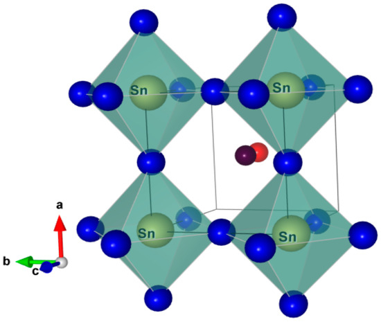
Figure 1.
Building Block of α-CH3NH3SnI3 [47] (COD Id = 4335632), Color code: I = Blue, Sn = Yellow, C = Red, N = Purple.

Table 1.
Simulation parameters for perovskite solar cell using SCAPS-1D.
The device configuration of the simulated FTO/PCBM/CH3NH3SnI3/CuO/Back metal (Structure 1), FTO/TiO2/CH3NH3SnI3/CuO/Back metal (Structure 2), FTO/WO3/ CH3NH3SnI3/CuO Back metal (Structure 3) solar cells and the corresponding band diagrams are shown in Figure 2a–c.
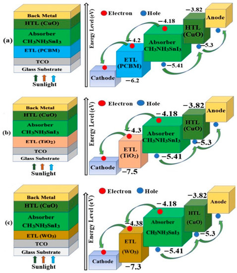
Figure 2.
Schematic diagram of proposed perovskite solar cell’s structure and Energy band alignment; (a) Structure 1, (b) Structure 2 and (c) Structure 3.
3. Results
3.1. Effect of Amphoteric Defect Density in the Absorber Layer
The impact of native imperfections on semiconductors is referred to as an “amphoteric defect” [62]. The fundamental characteristic of this type of defect is the Fermi level stabilization energy (EFS) [63]. Even though in balanced growth conditions for any thin film, native faults are natural components that are practically intrinsic in crystal structures [64], these defects produce short minority carrier lifetimes, resulting in lower Voc in solar cells [65].
The thickness of the absorber layer is considered 0.7 µm, as established by a prior study [66]. Figure 3 shows the impact of amphoteric defects on the absorber layer when defect concentration is raised from 1011 cm−3 to 1016 cm−3. We noticed that Voc and Jsc are virtually identical up to the defect concentration of 1015 cm−3. When the defect concentration is boosted from 1015 cm−3 to 1016 cm−3, Voc, Jsc and FF decrease drastically. For the device structures 1 (Figure 2a) and 2 (Figure 2b), the Voc reduced from approximately 0.8 V to about 0.7 V (Figure 3a,b) and Voc dropped from 0.89 V to about 0.69 V for Structure 3 (Figure 3c) at 1016 cm−3 defect density. Figure 3d illustrates the impact of defect density on Jsc and FF for three different ETLs on SnX3-based perovskite structures. Jsc decreased from 35.02 mA/cm2 to 27.49 mA/cm2, 36.71 mA/cm2 to 30.76 mA/cm2, 36.71 mA/cm2 to 22.91 mA/cm2 for structures 1, 2 and 3, respectively. FF is decreased from 76.12% to 59.45%, 78.57% to 61.98% and 73.23% to 59.23% for structures 1, 2 and 3, respectively. With the defect concentration from 1015 cm−3 to 1016 cm−3, PCE is decreased 21.32% to 11.37%, 23.61% to 13.51% and 23.97% to 7.74% for the structures 1, 2 and 3, respectively. The negative impact on solar cell performance may be due to the greater recombination rates and shorter diffusion times for photogenerated charge carriers derived from higher defect densities, so in each case, the defect tolerance limit for the proposed structures is considered 1015 cm−3.
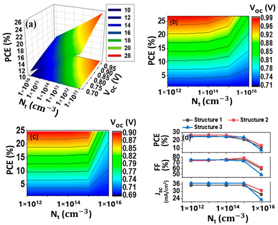
Figure 3.
Effect of amphoteric defect concentration (Nt) in absorber (i-layer); PCE and Voc vs. amphoteric defect concentration (Nt) for (a) Structure 1, (b) Structure 2 and (c) Structure 3, (d) PCE, FF and Jsc vs. amphoteric defect concentration (Nt).
3.2. Effect of Interfacial Defect Density ETL/CH3NH3SnI3 (IL1) and CH3NH3SnI3/CuO (IL2)
To improve cell efficiency, recombination loss at interfaces should be reduced [67]. Recently, considerable approaches have been described for interface remodelling to avoid recombination [68,69,70,71]. In this simulation defect states were investigated in both interface layers ETL/CH3NH3SnI3 and CH3NH3SnI3/CuO.
For IL1, single energetic distribution has been considered. Figure 4b shows that with the IL1 defect condition for device 2, virtually there is no significant changes occurred on the cell performance. Voc is almost constant up to the defect density of 1016 cm−3. Moreover, it is seen that when defect density rises from 1011 cm−3 to 1017 cm−3, Voc drops continuously from 0.97 V to 0.7 V and 0.85 V to 0.57 V for structures 1 and 3, respectively (Figure 4a,c). As seen in Figure 4d, with the increasing defect concentration up to 1015 cm−3 no significant changes occurred for Jsc for all structures. Above this concentration Jsc drastically decrease for structures 1 and 3. For device 2, no significant changes occurred on FF up to defect density of 1016 cm−3 but above this density a marginal increase of FF is observed. FF is decreased drastically for structures 1 and 3 above the defect concentration of 1014 cm−3. PCE remains almost constant for structure 2. But PCE decreased significantly from the defect density of 1 × 1013 cm−3 and 1 × 1012 cm−3 for structures 1 and 3, respectively. PCE is decreased mainly due to the decrement of Voc. So, IL1 defect tolerance limit of structure 1 is 1 × 1013 cm−3 and structure 3 is 1 × 1012 cm−3. Low defect tolerance limit may be due to extensive carrier recombination at the interface and lower the device performance [72]. A defect tolerance limit may be predicted at interface TiO2/CH3NH3SnI3 for structure 2 is 1 × 1016 cm−3. The high defect tolerance limit of the device indicates a well-matched conduction band offset between TiO2 and perovskite, which creates an effective interfacial electric field that prompts carrier extraction, resulting in improved cell stability and performance [73]. The higher defect tolerance limit at the interface, making it more appropriate for fabrication.
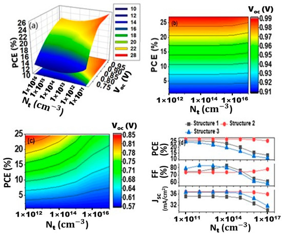
Figure 4.
Effect of interfacial defect concentration (Nt) at ETL/Absorber layer; PCE and Voc vs. interfacial defect concentration for (a) Structure 1, (b) Structure 2 and (c) Structure 3, (d) Jsc, FF and PCE vs. the interfacial defect concentration in IL1.
As seen from Figure 5a, cell efficiency has dropped when the defect density at IL2 raised to 1 × 1014 cm−3 or higher, from 25.39% to 23.14%, 26.85% to 24.56% and 24.63% to 21.62% for structures 1, 2 and 3, respectively. With increasing defect density Voc drops from around 0.99 V to 0.80 V for structures 1 and 2 (Figure 5a,b). For device 3, Voc drops from about 0.99 V to 0.80 V (Figure 5c). Above a defect density of 1 × 1014 cm−3, a drastic decrement of Voc is observed in all cases. The recombination rate increases as the defect density state at the interface rise, causing the reverse saturation current to increase and the open-circuit voltage to drop. PCE is decreased mainly due to the decrement of Voc. The relationship between Jsc, FF, PCE, and defect states in the CH3NH3SnI3/CuO interface is shown in Figure 5d. There are no significant changes that occurred for Jsc with increasing the defect density for all three proposed structures. Above the defect density of 1014 cm−3, FF is increased for structures 1 and 2, but a negligible decrement is observed for structure 3. The ideality factor (n), which is linked to the nature of the semiconductor, influences carrier generation, its transportation at the interface and collection at the terminal contact. An increase in the ideality factor has a direct and negative effect on the fill factor of solar cells [74]. For structures 1 and 2, the FF increment indicates a low ideality factor and a reduction in reverse saturation current above a defect density of 1014 cm−3. Variations in the amount of defect state have been shown to have a greater influence on Voc than Jsc. As a result, changes in Voc are primarily responsible for the device’s decreased efficiency. Consequently, the CH3NH3SnI3/CuO interface defect tolerance is considered 1014 cm−3, as the efficiency of each device falls considerably over that limit.
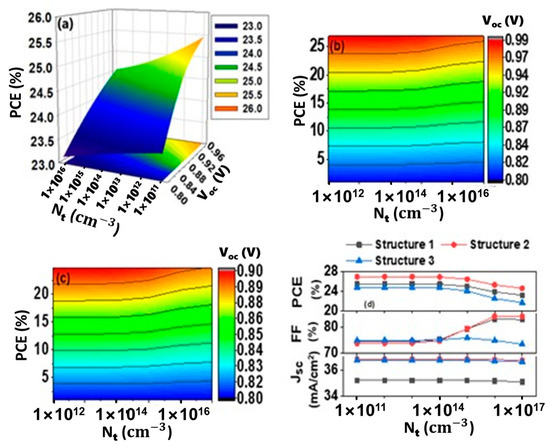
Figure 5.
Effect of interfacial defect concentration (Nt) at IL2 interface; PCE and Voc vs. interfacial defect concentration for (a) Structure 1, (b) Structure 2 and (c) Structure 3, (d) Jsc, FF and efficiency vs. interfacial defect concentration in IL2.
3.3. Metal Work Function
The amount of energy or photons required to remove an electron from a metal’s surface is known as its work function. It has been found that a larger work function value increases solar cell efficiency. This is due to the fact that when the work function value increases, the majority carrier’s barrier height drops, making contact more ohmic in nature. The effect of various metals as back contact electrodes on the performance of PSCs has been investigated as represented in Table 2.
Table 2.
Metal work function of back contact material.
Simulations have been done using copper (Cu), carbon (C), nickel (Ni) and gold (Au) as prospective back contacts for perovskite solar cells. An Ohmic contact between ETL and electrode is required for the smooth collection of electrons to the load [79]. A relatively high work function is appropriate for back contact materials. From Figure 6, it is seen that with increasing work function of back contact materials, the efficiency of perovskite solar cells increases. It is found that Au as a back electrode material indicates the highest efficiency of 24.58% for device 1, 26.02% for device 2 and 23.53% for device 3. In comparison best performance of the cell is obtained when TiO2 is used as ETL material in device 2.
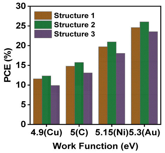
Figure 6.
Solar cell efficiency for different back contact metals.
3.4. C-V Characteristics of the Cell
A built-in potential (Vbi) is required to move photogenerated holes and electrons in opposing directions [80]. The junction potential difference in a solar cell generates Vbi. High built-in potential is required to prevent significant losses due to carrier recombination processes in solar cells in order to ensure effective energy conversion. In this work Schottky contact is formed in ETL/Front contact. Vbi can be obtained from a Mott-Schottky capacitance study. A space charge effect is responsible for the rise in capacitance. When the voltage rises, the depletion width narrows, resulting in an increase in capacitance. Following a particular voltage drive, the capacitance is again declined and can even be negative. Recombination or self-heating can generate negative capacitances as well [81]. Mott-Schottky analysis is a prominent method to obtain doping concentration and the built-in voltage which is expressed by the following relationship:
where C = capacitance, S = area, ε = vacuum permittivity, NA = dopant density and Vbi = built-in- voltage. Figure 7X,Y show that the C-V and Mott-Schottky plot and simulation features, respectively, as a function of ETL’s shallow uniform donor density (Nd) for three simulated devices (Figure 7a–c). A simulation was done for donor density (Nd), where concentration was ranged from 1016 cm−3 to 1020 cm−3, keeping other factors as constant. We know that carrier recombination solely takes place at the donor-acceptor interface where Voc does not affect the built-in voltage. On the other hand, the fill factor (FF) is significantly lowered when the built-in voltage drops below the open-circuit voltage [82]. In this study, it has been found that with the voltage applied, capacitance increases gradually and rises sharply when the Nd is 1020 cm−3. The Vbi is obtained from the voltage axis intersect. The built-in potential (Vbi) has been found to increase from 0.71 V to 0.78 V with the increase of Nd for structures 1 and 2 (Figure 7(Ya,b)), but for Structure 3, it is ranged from 0.44 to 0.65 V (Figure 7(Yc)). This means that a greater carrier recombination rate reduces the Vbi value in structure 3. High built-in potential for structures 1 and 2 denotes the rapid movement of the photogenerated holes and electrons in opposing directions makes the devices for a better choice of fabrication.
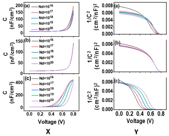
Figure 7.
(X) Capacitance–voltage characteristics, (Y) Mott-Schottky plot for the PCSs, (a) Structure 1, (b) Structure 2, (c) Structure 3, measured as a function of ETL donor density.
3.5. Effect of Series Resistance
The performance of perovskite solar cells is limited due to the series resistance of the device. In an ideal solar cell, series resistance (RS) will be zero and shunt resistance (RSH) should be infinitive [83]. The transparent conductive oxide layer is one of the primary contributors to the series resistance (RS) [84]. Rs is derived from current flow resistance in PSCs, in particular through interfaces [72]. The FF of the device is influenced by its RS and RSH [85]. Excessive series resistance values (RS) can also lower the Jsc. The relationship of output current and the series resistance is given below:
Here, I = output current, IL = light generated current, RSH = shunt resistance and RS = series resistance, q and k are constants, T = absolute temperature. The FF and PCE with series resistances (Rs) on the proposed CH3NH3SnI3 based three solar cell structures are shown in Figure 8. It has been found that increasing series resistance has a negative impact mostly on the FF due to solder bond degradation [86].
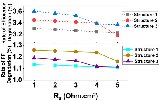
Figure 8.
The rate of change of FF and PCE with respect to series resistances (Rs).
The solder bond undergoes fatigue or cracks in an open environment that leads to increasing series resistance. The series resistance correlates to a drop in fill factor (FF) as follows [87]:
ΔFF = −(Jsc/Voc) × Rs(total) × FFideal
Once Rs is unusually high, it has a little observed impact on the Jsc. Figure 8 shows that above Rs = 3 ohm·cm2, FF degrades dramatically for structures 2 and 3. That’s because the interface solder bonding may not be strong enough at a higher Rs value. Due to relatively strong interface solder bonding for structure 1, the rate of efficiency and FF degradation is virtually constant. The FF degradation rate of solar cells is about 3.4 ± 0.2% per 1 Ω rise in Rs, which is much lower than that of typical Si solar cells (roughly 2.5 percent for 0.1 increase in Rs). The FF of the Si solar cell reduces by about 2.5% each time the series resistance increases by 0.1 Ω [88]. However, whereas FF declines at 3.4 ± 0.2%, efficiency only decreases at 1.15 ± 0.1% with a 1 rise in Rs. The proposed solar cell structures are much better than the conventional Si solar cell in terms of series resistance.
3.6. Effect of Temperature
Working temperatures significantly influence perovskite solar cell performance, as they are placed in an open environment. The effect of temperature has been investigated from 300 K to 400 K, and the result shows that cell performance is greatly influenced by temperature, as seen in Figure 9. Cell efficiency is lowered with temperature rises because photovoltaic parameters (i.e., bandgap, electron and hole mobility, and carrier concentration) are influenced by higher temperatures [89]. The following equation is used to determine the open-circuit voltage (Voc) of a solar cell [90]:
where, K = Boltzmann constant, T = absolute temperature in Kelvin and J0 = reverse saturation current. According to Equation (1), a low reverse saturation current is necessary to increase Voc. Reverse saturation current is responsible for the decrement of Voc as temperature rises. The hypothesis might be that the peripheral increase of Jsc with temperature that the bandgap in the semiconductor will be reduced with the increasing temperature [91]. Interatomic spacing of atoms of semiconductors increases with temperature hence decrease the band gap. In general, when temperature rises, electrical mobility and conductivity increases [92]. As seen from Figure 9, there is no significant change of Jsc with temperature for structures 1 and 2. A decrease in Jsc with high temperature has occurred for Structure 3 might be due to the fact the electrons are unstable at high temperature and recombine with the holes [93]. Lattice scattering is the primary process that influences electron and hole mobility as frequency scattering rises with temperature, so at high temperatures the carrier mobility should decrease, and the resistivity will increase.
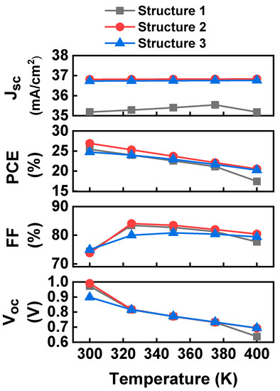
Figure 9.
Effect of temperature on cell performance.
As observed from Figure 10, the efficiency of the proposed three perovskite solar cells with PCBM, TiO2 and WO3 ETLs decreases as the temperature rises. For Structure 1, the efficiency is decreased at around 0.058%/K, but at higher temperature (400 K) the value is 0.15%/K. In case of Structure 2 the degradation gradient is almost constant at the value of 0.064 a.u. The degradation gradient decreases exponentially with temperature for structure 3 but the value is lower than that of structures 1 and 2 makes it more thermal stable. At higher temperature structures 2 and 3 provide more thermal stability than Structure 1. The low value of the degradation gradient indicates the possibility of real device fabrication for all the proposed three structures.
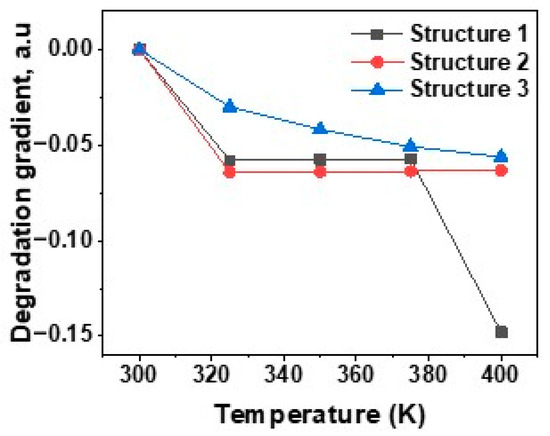
Figure 10.
Degradation gradient of PSC for different electron transport layers.
4. Conclusions
In this work, SCAPS software was utilized to conduct a comprehensive simulation analysis on the lead-free CH3NH3SnI3 perovskite materials featuring superior optoelectronic characteristics and environmental effects. The numerical simulation is mostly concerned with temperature, amphoteric defects of the absorber layer, and defect study of the interfaces. A comparative study of three devices was performed. In every case the device works best at room temperature. It is suggested to install the devices with a cooling water system to reduce the carrier’s thermal scattering and heating effect. With an amphoteric defect density of more than 1015 cm−3 the device performance was greatly reduced. Interfaces defect tolerance limit for IL1 is 1013 cm−3, 1016 cm−3, 1012 cm−3 for structures 1, 2 and 3 respectively. Interfaces defect tolerance limit for IL2 was found 1014 cm−3. The device structure of FTO/TiO2/CH3NH3SnI3/CuO/back electrode exhibits a better defect tolerance limit. It is found that the use of Au as a back-contact material provides the highest efficiencies of 25.45%, 26.92% and 24.73% for structures 1, 2 and 3, respectively. This simulation shows that eco-friendly CH3NH3SnI3 can be used as a high-efficiency photovoltaic device.
Author Contributions
M.M.: writing—original draft; K.S. (K. Sobayel): conceptualization, software & formal analysis; D.S.: review & editing; S.A.: writing—review & editing; H.A.: validation & visualization; M.S.: editing & visualization; K.T.: project administration & funding acquisition; N.A.: review & editing; K.S. (Kamaruzzaman Sopian): validation & visualization; M.A.: supervision & writing—review & editing. All authors have read and agreed to the published version of the manuscript.
Funding
The research is supported by Universiti Kebangsaan Malaysia, Malaysia for financial support through Long-term Research Grant Scheme (LRGS/1/2019/UKM-UKM/6/1) and the Postdoctoral Fellowship from Prince of Songkla University. This research is also supported by Taif University Researchers Supporting Project Number (TURSP-2020/248).
Institutional Review Board Statement
Not applicable.
Informed Consent Statement
Not applicable.
Data Availability Statement
Data will be made available upon a reasonable request to the corresponding author.
Acknowledgments
We acknowledge the Universiti Kebangsaan Malaysia, Malaysia for financial support through Long-term Research Grant Scheme (LRGS/1/2019/UKM-UKM/6/1). The research is supported by the Postdoctoral Fellowship from Prince of Songkla University. The authors would also like to acknowledge the support from Taif University Researchers Supporting Project Number (TURSP-2020/248), Taif University, Taif, Saudi Arabia. The authors gratefully acknowledge Marc Burgelman, University of Gent, Belgium, for providing the SCAPS simulation software.
Conflicts of Interest
The authors declare no conflict of interest.
List of Abbreviation
| Abbreviation | Meaning |
| ETL | Electron transport layer |
| HTL | Hole transport layer |
| PCE | Power conversion efficiency |
| Jsc | Short circuit current |
| Voc | Open circuit voltage |
| J0 | Reverse saturation current |
| FF | Fill factor |
| FTO | Fluorine doped tin oxide |
| IDL | Interface defect layer |
| IL | Interface layer |
| COD | Crystallography Open Database |
References
- Izadi, F.; Ghobadi, A.; Gharaati, A.; Minbashi, M.; Hajjiah, A. Effect of interface defects on high efficient perovskite solar cells. Optik 2021, 227, 166061. [Google Scholar] [CrossRef]
- Raj, A.; Kumar, M.; Bherwani, H.; Gupta, A.; Anshul, A. Evidence of improved power conversion efficiency in lead-free CsGeI3 based perovskite solar cell heterostructure via scaps simulation. J. Vac. Sci. Technol. B 2021, 39, 012401. [Google Scholar] [CrossRef]
- Lu, H.; Krishna, A.; Zakeeruddin, S.M.; Grätzel, M.; Hagfeldt, A. Compositional and Interface Engineering of Organic-Inorganic Lead Halide Perovskite Solar Cells. iScience 2020, 23, 101359. [Google Scholar] [CrossRef]
- Lazemi, M.; Asgharizadeh, S.; Bellucci, S. A computational approach to interface engineering of lead-free CH3NH3SnI3 highly-efficient perovskite solar cells. Phys. Chem. Chem. Phys. 2018, 20, 25683–25692. [Google Scholar] [CrossRef]
- Yue, S.; McGuire, S.C.; Yan, H.; Chu, Y.S.; Cotlet, M.; Tong, X.; Wong, S.S. Synthesis, Characterization, and Stability Studies of Ge-Based Perovskites of Controllable Mixed Cation Composition, Produced with an Ambient Surfactant-Free Approach. ACS Omega 2019, 4, 18219–18233. [Google Scholar] [CrossRef]
- Tuohey, H.; Della Gaspera, E.; Van Embden, J. Perovskite-Inspired High Stability Organometal Antimony(V) Halide Thin Films by Post-Deposition Bromination. ACS Mater. Lett. 2020, 2, 1203–1210. [Google Scholar] [CrossRef]
- Kopacic, I.; Friesenbichler, B.; Hoefler, S.F.; Kunert, B.; Plank, H.; Rath, T.; Trimmel, G. Enhanced Performance of Germanium Halide Perovskite Solar Cells through Compositional Engineering. ACS Appl. Energy Mater. 2018, 1, 343–347. [Google Scholar] [CrossRef]
- Chen, M.; Ju, M.G.; Carl, A.D.; Zong, Y.; Grimm, R.L.; Gu, J.; Zeng, X.C.; Zhou, Y.; Padture, N.P. Cesium Titanium(IV) Bromide Thin Films Based Stable Lead-free Perovskite Solar Cells. Joule 2018, 2, 558–570. [Google Scholar] [CrossRef]
- Wan, Z.; Lai, H.; Ren, S.; He, R.; Jiang, Y.; Luo, J.; Chen, Q.; Hao, X.; Wang, Y.; Zhang, J.; et al. Interfacial engineering in lead-free tin-based perovskite solar cells. J. Energy Chem. 2021, 57, 147–168. [Google Scholar] [CrossRef]
- Tai, Q.; Cao, J.; Wang, T.; Yan, F. Recent advances toward efficient and stable tin-based perovskite solar cells. EcoMat 2019, 1, e12004. [Google Scholar] [CrossRef]
- Shum, K.; Tsatskina, A. Solar cells: Stabilizing tin-based perovskites. Nat. Energy 2016, 1, 1–2. [Google Scholar] [CrossRef]
- Cao, J.; Yan, F. Recent progress in tin-based perovskite solar cells. Energy Environ. Sci. 2021, 14, 1286–1325. [Google Scholar] [CrossRef]
- Rühle, S. Tabulated values of the Shockley–Queisser limit for single junction solar cells. Sol. Energy 2016, 130, 139–147. [Google Scholar] [CrossRef]
- Jeong, J.; Kim, M.; Seo, J.; Lu, H.; Ahlawat, P.; Mishra, A.; Yang, Y.; Hope, M.A.; Eickemeyer, F.T.; Kim, M.; et al. Pseudo-halide anion engineering for α-FAPbI3 perovskite solar cells. Nature 2021, 592, 381–385. [Google Scholar] [CrossRef] [PubMed]
- Jiang, X.; Chen, S.; Li, Y.; Zhang, L.; Shen, N.; Zhang, G.; Du, J.; Fu, N.; Xu, B. Direct Surface Passivation of Perovskite Film by 4-Fluorophenethylammonium Iodide toward Stable and Efficient Perovskite Solar Cells. ACS Appl. Mater. Interfaces 2021, 13, 2558–2565. [Google Scholar] [CrossRef]
- He, Q.; Worku, M.; Xu, L.; Zhou, C.; Lteif, S.; Schlenoff, J.B.; Ma, B. Surface passivation of perovskite thin films by phosphonium halides for efficient and stable solar cells. J. Mater. Chem. A 2020, 8, 2039–2046. [Google Scholar] [CrossRef]
- Wang, R.; Wang, J.; Tan, S.; Duan, Y.; Wang, Z.K.; Yang, Y. Opportunities and Challenges of Lead-Free Perovskite Optoelectronic Devices. Trends Chem. 2019, 1, 368–379. [Google Scholar] [CrossRef]
- Tai, Q.; Guo, X.; Tang, G.; You, P.; Ng, T.-W.; Shen, D.; Cao, J.; Liu, C.-K.; Wang, N.; Zhu, Y.; et al. Antioxidant Grain Passivation for Air-Stable Tin-Based Perovskite Solar Cells. Angew. Chem. 2019, 131, 816–820. [Google Scholar] [CrossRef]
- Bi, C.; Zheng, X.; Chen, B.; Wei, H.; Huang, J. Spontaneous Passivation of Hybrid Perovskite by Sodium Ions from Glass Substrates: Mysterious Enhancement of Device Efficiency Revealed. ACS Energy Lett. 2017, 2, 1400–1406. [Google Scholar] [CrossRef]
- Zhang, F.; Zhang, Q.; Liu, X.; Hu, Y.; Lou, Z.; Hou, Y.; Teng, F. Property Modulation of Two-Dimensional Lead-Free Perovskite Thin Films by Aromatic Polymer Additives for Performance Enhancement of Field-Effect Transistors. ACS Appl. Mater. Interfaces 2021, 13, 20. [Google Scholar] [CrossRef]
- Du, X.; Qiu, R.; Zou, T.; Chen, X.; Chen, H.; Zhou, H. Enhanced Uniformity and Stability of Pb–Sn Perovskite Solar Cells via Me4NBr Passivation. Adv. Mater. Interfaces 2019, 6, 1900413. [Google Scholar] [CrossRef]
- Obila, J.O.; Lei, H.; Ayieta, E.O.; Ogacho, A.A.; Aduda, B.O.; Wang, F. Improving the efficiency and stability of tin-based perovskite solar cells using anilinium hypophosphite additive. New J. Chem. 2021, 45, 8092–8100. [Google Scholar] [CrossRef]
- Heo, J.H.; Kim, J.; Kim, H.; Moon, S.H.; Im, S.H.; Hong, K.H. Roles of SnX2 (X = F, Cl, Br) Additives in Tin-Based Halide Perovskites toward Highly Efficient and Stable Lead-Free Perovskite Solar Cells. J. Phys. Chem. Lett. 2018, 9, 6024–6031. [Google Scholar] [CrossRef]
- Sandhu, S.; Singh, R.; Yoo, K.; Kumar, M.; Lee, J.J. Effect of binary additives in mixed 2D/3D Sn-based perovskite solar cells. J. Power Sources 2021, 491, 229574. [Google Scholar] [CrossRef]
- Tang, G.; Li, S.; Cao, J.; Wang, T.; You, P.; Tai, Q.; Yan, F. Synergistic effects of the zinc acetate additive on the performance enhancement of Sn-based perovskite solar cells. Mater. Chem. Front. 2021, 5, 1995–2000. [Google Scholar] [CrossRef]
- Amine Additives Enable Self-Healing Lead-Free Perovskite Solar Cells. Available online: https://www.cambridge.org/core/journals/mrs-bulletin/news/amine-additives-enable-self-healing-lead-free-perovskite-solar-cells (accessed on 3 July 2021).
- Dai, Z.; Tang, W.; Wang, T.; Lv, T.; Luo, X.; Cui, D.; Sun, R.; Qiao, L.; Chen, H.; Zheng, R.; et al. Stable tin perovskite solar cells enabled by widening the time window for crystallization. Sci. China Mater. 2021, 64, 1849–1857. [Google Scholar] [CrossRef]
- Reo, Y.; Zhu, H.; Go, J.Y.; In Shim, K.; Liu, A.; Zou, T.; Jung, H.; Kim, H.; Hong, J.; Han, J.W.; et al. Effect of Monovalent Metal Iodide Additives on the Optoelectric Properties of Two-Dimensional Sn-Based Perovskite Films. Chem. Mater. 2021, 33, 2498–2505. [Google Scholar] [CrossRef]
- Nishimura, K.; Kamarudin, M.A.; Hirotani, D.; Hamada, K.; Shen, Q.; Iikubo, S.; Minemoto, T.; Yoshino, K.; Hayase, S. Lead-free tin-halide perovskite solar cells with 13% efficiency. Nano Energy 2020, 74, 104858. [Google Scholar] [CrossRef]
- Jiang, X.; Wang, F.; Wei, Q.; Li, H.; Shang, Y.; Zhou, W.; Wang, C.; Cheng, P.; Chen, Q.; Chen, L.; et al. Ultra-high open-circuit voltage of tin perovskite solar cells via an electron transporting layer design. Nat. Commun. 2020, 11, 1–7. [Google Scholar] [CrossRef] [PubMed]
- Zhu, K.; Neale, N.R.; Miedaner, A.; Frank, A.J. Enhanced Charge-Collection Efficiencies and Light Scattering in Dye-Sensitized Solar Cells Using Oriented TiO2 Nanotubes Arrays. Nano Lett. 2006, 7, 69–74. [Google Scholar] [CrossRef] [PubMed]
- Gheno, A.; Thu Pham, T.T.; Di Bin, C.; Bouclé, J.; Ratier, B.; Vedraine, S. Printable WO3 electron transporting layer for perovskite solar cells: Influence on device performance and stability. Sol. Energy Mater. Sol. Cells 2017, 161, 347–354. [Google Scholar] [CrossRef]
- Pitchaiya, S.; Natarajan, M.; Santhanam, A.; Asokan, V.; Yuvapragasam, A.; Madurai Ramakrishnan, V.; Palanisamy, S.E.; Sundaram, S.; Velauthapillai, D. A review on the classification of organic/inorganic/carbonaceous hole transporting materials for perovskite solar cell application. Arab. J. Chem. 2020, 13, 2526–2557. [Google Scholar] [CrossRef]
- Mahmood, K.; Sarwar, S.; Mehran, M.T. Current status of electron transport layers in perovskite solar cells: Materials and properties. RSC Adv. 2017, 7, 17044–17062. [Google Scholar] [CrossRef]
- Ali, F.; Pham, N.D.; Fan, L.; Tiong, V.; Ostrikov, K.; Bell, J.M.; Wang, H.; Tesfamichael, T. Low Hysteresis Perovskite Solar Cells Using an Electron-Beam Evaporated WO3–x Thin Film as the Electron Transport Layer. ACS Appl. Energy Mater. 2019, 2, 5456–5464. [Google Scholar] [CrossRef]
- Song, J.-X.; Yin, X.-X.; Li, Z.-F.; Li, Y.-W. Low-temperature-processed metal oxide electron transport layers for efficient planar perovskite solar cells. Rare Met. 2021, 40, 2730–2746. [Google Scholar] [CrossRef]
- Cocke, D.L.; Chuah, G.K.; Kruse, N.; Block, J.H. Copper oxidation and surface copper oxide stability investigated by pulsed field desorption mass spectrometry. Appl. Surf. Sci. 1995, 84, 153–161. [Google Scholar] [CrossRef]
- Yang, Z.; Wang, Y.; Liu, Y. Stability and charge separation of different CH3NH3SnI3/TiO2 interface: A first-principles study. Appl. Surf. Sci. 2018, 441, 394–400. [Google Scholar] [CrossRef]
- Hima, A. Enhancing of CH3NH3SnI3 based solar cell efficiency by ETL engineering. Int. J. Energy 2020, 5, 27. [Google Scholar] [CrossRef]
- Shamna, M.S.; Nithya, K.S.; Sudheer, K.S. Simulation and optimization of CH3NH3SnI3 based inverted perovskite solar cell with NiO as Hole transport material. Mater. Today Proc. 2020, 33, 1246–1251. [Google Scholar] [CrossRef]
- Bhandari, S.; Roy, A.; Ghosh, A.; Mallick, T.K.; Sundaram, S. Performance of WO3-Incorporated Carbon Electrodes for Ambient Mesoscopic Perovskite Solar Cells. ACS Omega 2019, 5, 422–429. [Google Scholar] [CrossRef]
- Devi, C.; Mehra, R. Device simulation of lead-free MASnI3 solar cell with CuSbS2 (copper antimony sulfide). J. Mater. Sci. 2019, 54, 5615–5624. [Google Scholar] [CrossRef]
- Wang, X.; Yao, Y.; Gao, W.; Zhan, Z. High-rate and high conductivity mesoporous TiO2 nano hollow spheres: Synergetic effect of structure and oxygen vacancies. Ceram. Int. 2021, 47, 13572–13581. [Google Scholar] [CrossRef]
- Mosconi, E.; Ronca, E.; Angelis, F. De First-Principles Investigation of the TiO2/Organohalide Perovskites Interface: The Role of Interfacial Chlorine. J. Phys. Chem. Lett. 2014, 5, 2619–2625. [Google Scholar] [CrossRef] [PubMed]
- Chen, L.C.; Chen, C.C.; Liang, K.C.; Chang, S.H.; Tseng, Z.L.; Yeh, S.C.; Chen, C.T.; Wu, W.T.; Wu, C.G. Nano-structured CuO-Cu2O Complex Thin Film for Application in CH3NH3PbI3 Perovskite Solar Cells. Nanoscale Res. Lett. 2016, 11, 402. [Google Scholar] [CrossRef]
- Hossain, M.I.; Alharbi, F.H.; Tabet, N. Copper oxide as inorganic hole transport material for lead halide perovskite based solar cells. Sol. Energy 2015, 120, 370–380. [Google Scholar] [CrossRef]
- Stoumpos, C.C.; Malliakas, C.D.; Kanatzidis, M.G. Semiconducting tin and lead iodide perovskites with organic cations: Phase transitions, high mobilities, and near-infrared photoluminescent properties. Inorg. Chem. 2013, 52, 9019–9038. [Google Scholar] [CrossRef] [PubMed]
- Kutlu, K.; Kavak, P.; Parlak, E.A.; Saatci, A.E.; Gökdemir, F.P.; Menda, U.D.; Özdemir, O. Energy-band diagram of PCDTBT, PCBM and blend by cyclic voltammetry and UV-visible measurements. In AIP Conference Proceedings; American Institute of Physics: New York, NY, USA, 2013. [Google Scholar]
- Gullapalli, S.K.; Vemuri, R.S.; Ramana, C.V. Structural transformation induced changes in the optical properties of nanocrystalline tungsten oxide thin films. Appl. Phys. Lett. 2010, 96, 171903. [Google Scholar] [CrossRef]
- Del Angel, R.; Durán-Álvarez, J.C.; Zanella, R. TiO2-Low Band Gap Semiconductor Heterostructures for Water Treatment Using Sunlight-Driven Photocatalysis. In Titanium Dioxide—Material for a Sustainable Environment; BoD–Books on Demand: Hamburg, Germany, 2018. [Google Scholar]
- Weiss, M.; Horn, J.; Richter, C.; Schlettwein, D. Preparation and characterization of methylammonium tin iodide layers as photovoltaic absorbers. Phys. Status Solidi Appl. Mater. Sci. 2016, 213, 975–981. [Google Scholar] [CrossRef]
- Noel, N.K.; Stranks, S.D.; Abate, A.; Wehrenfennig, C.; Guarnera, S.; Haghighirad, A.A.; Sadhanala, A.; Eperon, G.E.; Pathak, S.K.; Johnston, M.B.; et al. Lead-free organic-inorganic tin halide perovskites for photovoltaic applications. Energy Environ. Sci. 2014, 7, 3061–3068. [Google Scholar] [CrossRef]
- Yankson, A.A.; Kuditcher, A.; Gebreyesus, G.; Egblewogbe, M.N.Y.H.; Amuzu, J.K.A.; Armah, E.A. A Low Cost Synthesis and Characterization of CuO Nanoparticles for Photovoltaic Applications. Ghana J. Sci. 2019, 60, 17–23. [Google Scholar] [CrossRef][Green Version]
- Otoufi, M.K.; Ranjbar, M.; Kermanpur, A.; Taghavinia, N.; Minbashi, M.; Forouzandeh, M.; Ebadi, F. Enhanced performance of planar perovskite solar cells using TiO2/SnO2 and TiO2/WO3 bilayer structures: Roles of the interfacial layers. Sol. Energy 2020, 208, 697–707. [Google Scholar] [CrossRef]
- Du, H.J.; Wang, W.C.; Zhu, J.Z. Device simulation of lead-free CH3NH3SnI3 perovskite solar cells with high efficiency. Chin. Phys. B 2016, 25, 108802. [Google Scholar] [CrossRef]
- Starowicz, Z.; Wisz, G.; Yavorskyi, R.; Zapukhlyak, Z.; Bester, M.; Głowa, Ł.; Sibiński, M.; Cholewa, M. Simulation of TiO2/CuO solar cells with SCAPS-1D software. Mater. Res. Express 2019, 6, 085918. [Google Scholar]
- Rai, S.; Pandey, B.K.; Dwivedi, D.K. Device simulation of low cost HTM free perovskite solar cell based on TiO2 electron transport layer. AIP Conf. Proc. 2020, 2220, 140022. [Google Scholar] [CrossRef]
- Bansal, S.; Aryal, P. Evaluation of new materials for electron and hole transport layers in perovskite-based solar cells through SCAPS-1D simulations. In Proceedings of the IEEE PVSC Conference, Washington, DC, USA, 25–30 June 2017. [Google Scholar] [CrossRef]
- Anwar, F.; Mahbub, R.; Satter, S.S.; Ullah, S.M. Effect of Different HTM Layers and Electrical Parameters on ZnO Nanorod-Based Lead-Free Perovskite Solar Cell for High-Efficiency Performance. Int. J. Photoenergy 2017, 2017, 9846310. [Google Scholar] [CrossRef]
- Li, Z.Q.; Ni, M.; Feng, X.D. Simulation of the Sb2Se3 solar cell with a hole transport layer. Mater. Res. Express 2019, 7, 016416. [Google Scholar] [CrossRef]
- Babu, B.J.; Mandadapu, U.; Vedanayakam, S.V.; Thyagarajan, K. Optimisation of high efficiency tin halide perovskite solar cells using SCAPS-1D. Int. J. Simul. Process Model. 2018, 13, 221. [Google Scholar] [CrossRef]
- Walukiewicz, W.; Rey-Stolle, I.; Han, G.; Jaquez, M.; Broberg, D.; Xie, W.; Sherburne, M.; Mathews, N.; Asta, M. Bistable Amphoteric Native Defect Model of Perovskite Photovoltaics. J. Phys. Chem. Lett. 2018, 9, 3878–3885. [Google Scholar] [CrossRef]
- Walukiewicz, W. Intrinsic limitations to the doping of wide-gap semiconductors. Phys. B Condens. Matter 2001, 302–303, 123–134. [Google Scholar] [CrossRef]
- Meggiolaro, D.; Motti, S.G.; Mosconi, E.; Barker, A.J.; Ball, J.; Andrea Riccardo Perini, C.; Deschler, F.; Petrozza, A.; De Angelis, F. Iodine chemistry determines the defect tolerance of lead-halide perovskites. Energy Environ. Sci. 2018, 11, 702–713. [Google Scholar] [CrossRef]
- Sobayel, K.; Akhtaruzzaman, M.; Rahman, K.S.; Ferdaous, M.T.; Al-Mutairi, Z.A.; Alharbi, H.F.; Alharthi, N.H.; Karim, M.R.; Hasmady, S.; Amin, N. A comprehensive defect study of tungsten disulfide (WS2) as electron transport layer in perovskite solar cells by numerical simulation. Results Phys. 2019, 12, 1097–1103. [Google Scholar] [CrossRef]
- Gagandeep; Singh, M.; Kumar, R.; Singh, V.; Srivastava, S. A theoretical comparison between CH3NH3PbI3 and CH3NH3SnI3 based solar cells. AIP Conf. Proc. 2020, 2265, 030609. [Google Scholar]
- Wolff, C.M.; Caprioglio, P.; Stolterfoht, M.; Neher, D. Nonradiative Recombination in Perovskite Solar Cells: The Role of Interfaces. Adv. Mater. 2019, 31, 1902762. [Google Scholar] [CrossRef] [PubMed]
- Xiong, S.; Hou, Z.; Zou, S.; Lu, X.; Yang, J.; Hao, T.; Zhou, Z.; Xu, J.; Zeng, Y.; Xiao, W.; et al. Direct Observation on p- to n-Type Transformation of Perovskite Surface Region during Defect Passivation Driving High Photovoltaic Efficiency. Joule 2021, 5, 467–480. [Google Scholar] [CrossRef]
- Jiang, Q.; Zhao, Y.; Zhang, X.; Yang, X.; Chen, Y.; Chu, Z.; Ye, Q.; Li, X.; Yin, Z.; You, J. Surface passivation of perovskite film for efficient solar cells. Nat. Photonics 2019, 13, 460–466. [Google Scholar] [CrossRef]
- Yoo, J.J.; Wieghold, S.; Sponseller, M.C.; Chua, M.R.; Bertram, S.N.; Hartono, N.T.P.; Tresback, J.S.; Hansen, E.C.; Correa-Baena, J.P.; Bulović, V.; et al. An interface stabilized perovskite solar cell with high stabilized efficiency and low voltage loss. Energy Environ. Sci. 2019, 12, 2192–2199. [Google Scholar] [CrossRef]
- Zheng, X.; Chen, B.; Dai, J.; Fang, Y.; Bai, Y.; Lin, Y.; Wei, H.; Zeng, X.C.; Huang, J. Defect passivation in hybrid perovskite solar cells using quaternary ammonium halide anions and cations. Nat. Energy 2017, 2, 1–9. [Google Scholar] [CrossRef]
- Pan, H.; Shao, H.; Zhang, X.L.; Shen, Y.; Wang, M. Interface engineering for high-efficiency perovskite solar cells. J. Appl. Phys. 2021, 129, 130904. [Google Scholar] [CrossRef]
- Minemoto, T.; Murata, M. Theoretical analysis on effect of band offsets in perovskite solar cells. Sol. Energy Mater. Sol. Cells 2015, 133, 8–14. [Google Scholar] [CrossRef]
- Vasić, A. The Influence of Ideality Factor on Fill Factor and Efficiency of Solar Cells. Mater. Sci. Forum 2000, 352, 241–246. [Google Scholar] [CrossRef]
- Derry, G.N.; Kern, M.E.; Worth, E.H. Recommended values of clean metal surface work functions. J. Vac. Sci. Technol. A Vac. Surf. Films 2015, 33, 060801. [Google Scholar] [CrossRef]
- Sultana, N.A.; Mahmood, Z.H. Utilization of low cost metals as back contact with Perovskite Solar Cell Utilization of low cost metals as back contact with Perovskite Solar Cell. Dhaka Univ. J. Appl. Sci. Eng. 2017, 4, 35–38. [Google Scholar]
- Ofuonye, B.; Lee, J.; Yan, M.; Sun, C.; Zuo, J.M.; Adesida, I. Electrical and microstructural properties of thermally annealed Ni/Au and Ni/Pt/Au Schottky contacts on AlGaN/GaN heterostructures. Semicond. Sci. Technol. 2014, 29, 095005. [Google Scholar] [CrossRef]
- Engelhart, D.P.; Wagner, R.J.V.; Johnsen, P.C.; Wodtke, A.M.; Schäfer, T. Adsorbate enhancement of electron emission during the quenching of metastable CO at metal surfaces. Phys. Chem. Chem. Phys. 2015, 17, 11540–11545. [Google Scholar] [CrossRef] [PubMed]
- Soucase, B.M.; Guaita Pradas, I.; Adhikari, K.R. Numerical Simulations on Perovskite Photovoltaic Devices. In Perovskite Materials—Synthesis, Characterisation, Properties, and Applications; InTech: Vienna, Austria, 2016. [Google Scholar]
- Poole, C.; Darwazeh, I. Microwave semiconductor materials and diodes. Microw. Act. Circuit Anal. Des. 2016, 355–393. [Google Scholar] [CrossRef]
- Knapp, E.; Ruhstaller, B. Analysis of negative capacitance and self-heating in organic semiconductor devices. J. Appl. Phys. 2015, 117, 135501. [Google Scholar] [CrossRef]
- Kirchartz, T.; Gong, W.; Hawks, S.A.; Agostinelli, T.; MacKenzie, R.C.I.; Yang, Y.; Nelson, J. Sensitivity of the mott-schottky analysis in organic solar cells. J. Phys. Chem. C 2012, 116, 7672–7680. [Google Scholar] [CrossRef]
- Zhang, L. Device Physics of Organic and Perovskite Solar Cells. Ph.D. Thesis, Iowa State University, Ames, IA, USA, 2015; p. 257. [Google Scholar]
- Baig, H.; Kanda, H.; Asiri, A.M.; Nazeeruddin, M.K.; Mallick, T. Increasing efficiency of perovskite solar cells using low concentrating photovoltaic systems. Sustain. Energy Fuels 2020, 4, 528–537. [Google Scholar] [CrossRef]
- Liao, P.; Zhao, X.; Li, G.; Shen, Y.; Wang, M. A new method for fitting current–voltage curves of planar heterojunction perovskite solar cells. Nano Micro Lett. 2018, 10, 1–8. [Google Scholar] [CrossRef]
- Tummala, A. Effect of Series Resistance Increase on Fill Factor of PV Cells Extracted from Field Aged Modules of Different Climates; Arizona State University: Tempe, AZ, USA, 2016. [Google Scholar]
- Meier, D.L.; Good, E.A.; Garcia, R.A.; Bingham, B.L.; Yamanaka, S.; Chandrasekaran, V.; Bucher, C. Determining components of series resistance from measurements on a finished cell. In Proceedings of the Conference Record 2006 IEEE 4th World Conference Photovoltaic Energy Conversion, WCPEC-4, Waikoloa, HI, USA, 7–12 May 2006; Volume 2, pp. 1315–1318. [Google Scholar] [CrossRef]
- Qi, B.; Wang, J. Fill factor in organic solar cells. Phys. Chem. Chem. Phys. 2013, 15, 8972–8982. [Google Scholar] [CrossRef]
- Nakada, T.; Mizutani, M. 18% efficiency Cd-free Cu(In, Ga)Se2 thin-film solar cells fabricated using chemical bath deposition (CBD)-ZnS buffer layers. Jpn. J. Appl. Phys. Part 2 Lett. 2002, 41, L165. [Google Scholar] [CrossRef]
- Katz, E.A.; Faiman, D.; Tuladhar, S.M.; Kroon, J.M.; Wienk, M.M.; Fromherz, T.; Padinger, F.; Brabec, C.J.; Sariciftci, N.S. Temperature dependence for the photovoltaic device parameters of polymer-fullerene solar cells under operating conditions. J. Appl. Phys. 2001, 90, 5343–5350. [Google Scholar] [CrossRef]
- Fan, H.Y. Temperature dependence of the energy gap in semiconductors. Phys. Rev. 1951, 82, 900–905. [Google Scholar] [CrossRef]
- Chirvase, D.; Chiguvare, Z.; Knipper, M.; Parisi, J.; Dyakonov, V.; Hummelen, J.C. Temperature dependent characteristics of poly(3 hexylthiophene)-fullerene based heterojunction organic solar cells. J. Appl. Phys. 2003, 93, 3376–3383. [Google Scholar] [CrossRef]
- Chelvanathan, P.; Hossain, M.I.; Amin, N. Performance analysis of copper-indium-gallium-diselenide (CIGS) solar cells with various buffer layers by SCAPS. Curr. Appl. Phys. 2010, 10, S387–S391. [Google Scholar] [CrossRef]
Publisher’s Note: MDPI stays neutral with regard to jurisdictional claims in published maps and institutional affiliations. |
© 2021 by the authors. Licensee MDPI, Basel, Switzerland. This article is an open access article distributed under the terms and conditions of the Creative Commons Attribution (CC BY) license (https://creativecommons.org/licenses/by/4.0/).