Abstract
Based on the standard 40 nm Complementary Metal Oxide Semiconductor (CMOS) process, a curvature compensation technique is proposed. Two low-voltage, low-power, high-precision bandgap voltage reference circuits are designed at a 1.2 V power supply. By adding IPTAT (positive temperature coefficient current) and ICTAT (negative temperature coefficient current) to the output resistance, the first-order compensation bandgap voltages can be obtained. Meanwhile, the third high-order compensation current is also superimposed on the same resistance. We make use of the collector current of the bipolar transistor to compensate for the nonlinear term of VBE. The simulation results show that TC (temperature coefficient) of the first circuit reference could be reduced from 29.1 × 10⁻⁶/°C to 5.71 × 10⁻⁶/°C over the temperature range of −25 to 125 °C after temperature compensation. The second one could be reduced from 17 × 10−6/°C to 5.22 × 10⁻⁶/°C.
1. Introduction
Reference voltage source circuit is an important unit module in integrated circuit design, which is widely used in analog integrated circuits, digital integrated circuits, and hybrid integrated circuits. The ideal voltage reference has some requirements are as follows:
- (1)
- Insensitive to temperature change;
- (2)
- Insensitive to power fluctuations;
- (3)
- Wide range of supply voltage;
- (4)
- Adjustable output voltage;
- (5)
- Low voltage and low power consumption.
Due to the advantages in the above aspects, the bandgap reference (BGR) is the mainstream reference source circuit at present. Nowadays, with the feature size of the integrated circuit is getting lower and lower, low-voltage, low power consumption, and high-precision bandgap reference circuits are necessary and have received widespread attention.
Many works [1,2,3] can achieve a high-precision reference voltage. Due to the limitation of the common-collector structure of the bipolar junction transistor, the reference voltage is higher than 1.2 V, and the minimum supply voltage must be higher than 1.4 V as well. To reduce the system voltage, researchers put forward various methods. H. Banba proposed the current mode structure [4] that could convert the sum of two currents to voltages, generate a temperature-independent reference, and also provide a practical pattern for the later low-voltage reference circuit.
The structure in the work of [5,6,7,8] achieves a sub-1 V voltage using the idea of [4]. K. J. Singh replaced the resistors of conventional bandgap voltage reference circuits with a stack of Metal-Oxide-Semiconductor Field-Effect Transistor (MOSFET) [9], thus resulting in the improvement in the area and low voltage. [10] CTAT voltage was divided, and PTAT voltage was multiplied to operate with a low input voltage. It was proposed that the circuit can generate a 0.8 V.
The temperature drift of the reference voltage has been another challenge in recent years. In order to reduce the temperature coefficient and improve the precision, many curvature compensation techniques have been presented. An exponential curvature compensation technique has been presented in the work of [11] by exploiting the temperature characteristics of the current gain ß of Bipolar Junction Transistors (BJTs). β changes with the temperature index, so a current that has a nonlinear relationship with the temperature can be obtained to compensate for the nonlinear term of the bandgap reference. However, the compensation in this work can only be applied for convex curves and is not suitable for concave curves. A piecewise-linear compensation was proposed in the work of [12]. The author divided the reference voltage curve into several parts within the whole temperature range and made a piecewise compensation for each part. In [13], a smoother reference voltage curve can be obtained by the superposition of two complementary reference voltages curves. The two paper have satisfactory compensation effects but double the layout area. Different kinds of resistors [14] have been incorporated into the compensation, aiming to cancel the nonlinear temperature dependence of the emitter-base voltage VEB. The method in this work has a high requirement on the type of resistance.
This paper adopted the square curvature compensation technology and designed two reference voltage source circuits. The compensation method in this paper is suitable for both the convex curves and the concave curves. Meanwhile, the simple structure will not waste too much layout area. This circuit only increases 3 µA current on the original basis. The collector current of the transistor was used to perform a nonlinear order compensation to reduce the influences of the nonlinear term on VBE. Compared with the first-order compensation reference voltage source, the power consumption of the new circuit only adds a few microwatts, which greatly reduces the temperature coefficient.
2. Principle of Bandgap Reference
The classical bandgap reference with the current mode structure is shown in Figure 1. The principle is to add two reverse temperature coefficient currents with different weights, getting a zero TC reference current at a certain temperature.
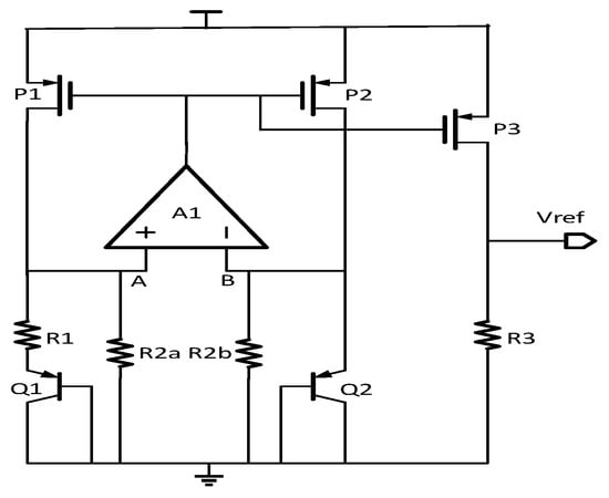
Figure 1.
Bandgap reference with current mode structure. P represents PMOSFET; R represents resistance; Q represents transistor.
The base-emitter junction of the PNP tube has a VBE-IC relationship given by
where IC is the collector current, and the saturation current IS is proportional to the base-emitter area.
The CTAT current is generated by a single BJT tube [8]. The analytical form of VBE is
where T0 is the reference temperature, Vg0 is the bandgap voltage of silicon at T0 and is 1.205 V at absolute temperature 0°, the temperature coefficient γ is approximately equal to 3, and JC is collector current density of PNP.
The relationship between JC and temperature can be expressed as
Bring (3) into the previous Formula (2) to obtain the final expression of VBE
where α is the order of the temperature behavior of the current.
In Equation (4), when VBE0 is approximately equal to 750 mV, T is 300 K, the value can be obtained by first-order partial derivative of VBE to temperature and is about −1.5 mV/°C. The voltage is negatively correlated with temperature.
In the structure in Figure 1, nodes A and B are forced to be at equal potential because of the feedback loop from the operational amplifier A1. So the CTAT current flowing in R2a is equal to the current flowing in R2b, which can be described as
The PTAT current flowing through resistance R1 can be described as
The first derivative of IPTAT with respect to temperature can be obtained and is about (0.086 × lnN)/R1 mV/°C. N is the ratio of the emitter area of two bipolar transistors generating positive TC voltage, and the voltage is proportional to temperature.
The low-voltage reference is generated by the sum of two currents, IPTAT and ICTAT, multiplied by the output resistor. IPTAT is produced from ∆VBE, and ICTAT is produced from VBE. The sum of IPTAT and ICTAT are copied from current mirrors P1, P2, and P3 to the output resistor. The first-order reference voltage is written as
N is the ratio of the emitter area of two bipolar transistors generating positive TC voltage. k is the Boltzmann constant, and q is the electric charger. VREF in this structure is adjustable. This structure is suitable for low voltage.
The Formulas (4)–(7) show that ∆VBE can only compensate for the linear term in VBE, but the high-order term cannot be compensated. So the temperature coefficient of the bandgap source after first-order compensation will not be small, especially in low-voltage structure, the voltage deviation will be amplified, and we will obtain a worse temperature coefficient, usually more than 30 × 10−6/°C. So other compensation ways are needed to obtain higher precision reference voltage.
A high-order compensation method was proposed in this article, and the principle is shown in Figure 2. The low-voltage reference is generated by three currents, namely, IPTAT, ICTAT, and INL, that are multiplied by the output resistor. IPTAT is produced from ∆VBE, and ICTAT is produced from VBE. The sum of these two opposite TC currents can present two typical curves, a convex curve, and a concave curve. The nonlinear compensation current INL from a nano-ampere curvature compensation module is to make a proper temperature compensation for different curvature curves, as illustrated in Figure 2. When the reference current forms a convex curve, the second derivative of its nonlinear term is less than zero. A current I2PTAT that is proportional to the square of temperature can make the compensation. By contrast, if the reference current forms a concave curve, the second derivative of its nonlinear term is greater than zero. The current −I2PTAT that is inversely proportional to the square of temperature can make the compensation.
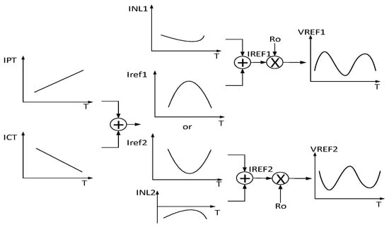
Figure 2.
Square curvature compensation principle. IPT represents IPTAT; ICT represents ICTAT; Iref1,2 represent two typical current curves after first-order temperature compensation; INL1,2 represent two non-linear compensation current; Vref1,2 represent reference voltage after high-order temperature compensation.
After curvature compensation, we can obtain output reference current IREF with:
Nonlinear compensation terms can be generated in different ways. In [11], INL is generated by the current difference between IPTTAT and IVBE, and the compensation current opens only at high temperatures. This reference circuit achieved a temperature drift of less than 20 ppm/°C at the temperature range of −15 to 90 °C. In [15], INL is generated by the base current of the bipolar transistor. However, the compensation is only used for convex curves.
3. Circuit Design
Two proposed low-voltage, high-precision bandgap circuit designs are shown in Figure 3 and Figure 4. The two circuit structures are slightly different in the high-order compensation circuit. Theoretically, the second-order derivative of the nonlinear part of VBE voltage is less than zero, and we obtain a downward V-T curve. However, in fact, because of the differences in current mirrors, bipolar transistors, op amps, or bias circuits, the second derivative of the nonlinear term of VREF may be greater than zero, and the V-T curve may open upward [16,17]. In the second case, we need to reverse INL to compensate.
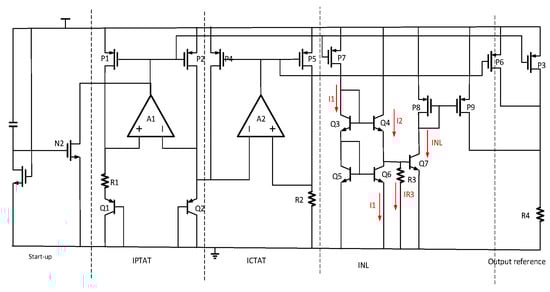
Figure 3.
Proposed the first bandgap reference.
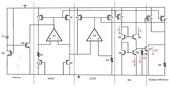
Figure 4.
Proposed the second bandgap reference.
3.1. Start-Up Circuit
The purpose is to prevent the degenerate state that the output of the op-amp is high and the input is low. The degenerate state makes the circuit unable to work normally, and the output keeps a low level for a long time. Furthermore, the essence of the degeneracy state is a metastable state and requires an external force to break the balance. The start-up circuit is such an external force. When the circuit works normally, the start-up circuit must be disconnected to keep the circuit stable. On the other hand, the start-up circuit designed in this paper is very simple in a structure consisting of only two MOSFETs and one capacitor. Due to the capacitor characteristics, when it is just powered on, the gate of N2 is high. After it is turned on, the gate voltage of P1 and P2 can be pulled down, and the two inputs of A1 and A2 amplifiers can be pulled up at the same time so that the circuit is out of degeneration. The gate of N1 connects to the power supply in a continuous conduction state, which can provide a discharge path for the C1 capacitor. After the discharge is completed, the gate of N2 is pulled down, and the start-up circuit disconnects. Considering the low-voltage structure, M3,4,9, and M10 can work in the subthreshold region.
3.2. Operational Amplifier Design
The operational amplifier designed in this circuit is displayed in Figure 5, and it is a folded-cascode amplifier. The operational amplifiers in bandgap reference circuits are used to generate positive temperature currents by clamping the transistor base-emitter voltage, and two-stage structures are frequently applied. On the contrary, the current mirror connected to the two-stage amplifier output is equivalent to a common source stage, and the three-stage structure will bring some problems to the stability of the whole bandgap circuit. The one-stage operational amplifier can bring favorable effects on circuit stability, while insufficient gain will result in larger system offset voltage, which is out of the designer’s expectations. For the advantages in sufficient gain, large output voltage swing, and suitable stability, the folded-cascode amplifier was used in our circuit.
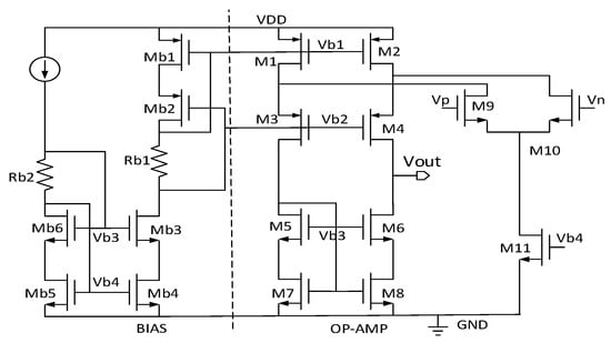
Figure 5.
Operational amplifier design. M1–11, b1–b6 are MOSFETs; vb1–4 are bias voltage; vp, vn are inputs.
Under the same conditions, the mobility of N-Metal-Oxide-Semiconductor (NMOS) is higher than that of P-Metal-Oxide-Semiconductor (PMOS), which is conducive to improving the response speed, and then M9, M10 are used as NMOS differential input pairs that also match the emitter-base voltage of transistor Q2 better. In the temperature range of −25 to 125 °C, the voltage of Vp and Vn will vary from 0.65 to 0.8V, and the threshold of NMOS and PMOS transistor is Vthn = 0.65 V and Vthp = −0.75 V, respectively, in this process. If PMOSFETs are used as the differential input pairs, the current mirror M11 will be forced into the linear region. In Figure 5, M1 and M2 provide the bias current of the input device. M3, M4, M9, and M10 form a cascode device. M5, M6, M7, and M8 are the load tubes, which affect the output impedance.
The gain of the cascode operational amplifier can be approximately expressed as:
where gmi is the transconductance of Mi, ro is the output resistance.
The loop gain and phase simulation is shown in Figure 6. The proposed operational amplifier has a DC loop gain of 63.6 dB and a phase margin of 60 degrees at 1.2 V supply voltage.
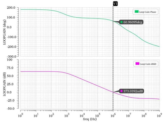
Figure 6.
Simulated loop response in Figure 5: Phase response and gain response (VDD = 1.2 V).
3.3. First-Order Temperature Compensation Circuit
The first-order temperature compensation circuit is slightly modified on the basis of the Banba structure, separating the positive temperature current generating circuit and the negative temperature current generating circuit. The purpose is to obtain separate PTAT current preparing for high-order temperature compensation. The PTAT and CTAT current generating circuits are symmetrical in structures. The obtained current flows through the output resistance by two sets of current mirrors. When the proportional relationship between R1 and R2 is adjusted reasonably, we can obtain nice first-order temperature compensation. The principle of temperature compensation has been explained in detail in Section 2, and I will not repeat it here. In this circuit structure, we choose N = 8. After calculation and further simulation, the ratio of R1 and R2 can be trimmed.
After first-order temperature compensation, the output voltage can be expressed as:
The simulation of temperature coefficient at the range of −25–125 °C after first-order temperature compensation was shown in Figure 6, Figure 7, Figure 8 and Figure 9.
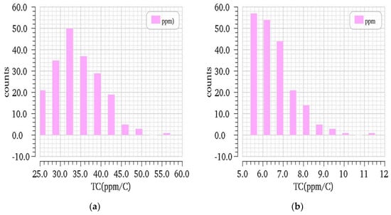
Figure 7.
In reference 1 (a) 200 Monte Carlo simulation results for TC after first-order temperature compensation; (b) 200 Monte Carlo simulation results for TC after high-order temperature compensation.
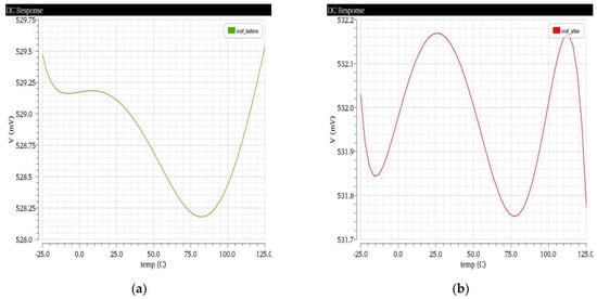
Figure 8.
In reference 2 (a) V-T curve after first-order temperature compensation; (b) V-T curve after high-order temperature compensation.
Figure 9.
In reference 2 (a) 200 Monte Carlo simulation results for TC after first-order temperature compensation; (b) 200 Monte Carlo simulation results for TC after high-order temperature compensation.
3.4. High-Order Temperature Compensation Circuit
The high-order temperature compensation circuit in Figure 3 is composed of a resistor, five Negative-Positive-Negative (NPN) bipolar transistors, and three PMOSFETs; two PMOSFETs were removed from the circuit in Figure 4 in order to obtain the opposite compensation.
Take circuit in Figure 3 as an example. According to Kirchhoff’s voltage law, VBE,Q7 can be expressed as:
Collector currents of Q3, Q5, Q6 copied from the current mirror are positive to temperature change (IPTAT). The current flowing through R3 is inversely proportional to the temperature (ICTAT):
The current flowing into Q4 is calculated as:
We assumed that each BJT has the same size, substituting the base-emitter voltage from (1) and current Formulas (12) and (13) into Equation (11), we can obtain the following expression:
From Equation (14), we can obtain the current flowing in Q7:
In order to make the TC of INL proportional to the square of the temperature, the denominator of formula (14) must be independent of temperature. We can adjust the ratio coefficient of R3, R2 to meet the requirements.
The output of the proposed design in Figure 2 and Figure 3 can be expressed in the form of
where the nonlinearities created by VBE can be compensated by INL, which is given in Equation (15). In Figure 4, we reverse IC and compensate for the high-order term of VREF, whose second derivative is positive.
4. Simulation Results
The simulation was carried out in candence software under the standard 40 nm CMOS process technology. The V-T curve of the structure in Figure 2 is exhibited in Figure 6. In a typical model, the power supply voltage is set to 1.2 V, the output voltage in reference 1 is 523 mV. When the temperature changes within the range of −25–125 °C, TC is 29.1 × 10⁻⁶/°C after the first-order compensation and is 5.71 × 10⁻⁶/°C after the second-order compensation. After the second-order compensation, the circuit power consumption only increases by a few microwatts and is only 30 uw, which meets the requirements of low voltage, low power consumption, and high precision. The output voltage in reference 2 is 533 mV. The V-T curve of the structure in Figure 3 is demonstrated in Figure 8. TC is reduced from 17 × 10−6/°C to 5.22 × 10⁻⁶/°C. Figure 7 and Figure 9 show 200 Monte Carlo simulation results of the temperature coefficient distribution. The proposed BGR at 1.2 V. Monte Carlo simulation reflects a probability distribution. Therefore, the simulation results of Figure 6 and Figure 8 are important examples of the results of Figure 7 and Figure 9.
Figure 10 plots the output reference voltage with the corresponding supply voltage at different temperatures. The supply voltage changes from 0 to 2 V, at −25, 27 and 125 °C, respectively. The simulation results prove that the BGR has a suitable linear adjustment rate. The minimum power supply voltage is 1V, and in the voltage range from 1 to 2 V, the bandgap reference voltage is stable.
Figure 10.
Reference voltage on the supply voltage in different operating temperatures (reference 2).
The simulation results of the bandgap reference voltage of −25 to 125 °C for various supply voltages are shown in Figure 11. The temperature coefficients at 1, 1.2, 1.4, 1.6, 1.8, and 2 V supply voltage are less than 10 × 10−6/°C. In particular, the accuracy of BGR is the highest at 1.2 V voltage.
Figure 11.
Reference voltage on the operating temperature in different supply voltage (reference 2).
Figure 12 shows that the reference circuit can start up normally in 3 us after the supply is turned on.
Figure 12.
Start-up time (reference 2).
5. Conclusions
In this paper, two bandgap references have been designed and simulated under a standard 40 nm CMOS process at a 1.2 V power supply. On the base of the model in [4], first-order temperature compensation, a second-order temperature compensation circuit is achieved. The collector current of the bipolar transistor can be used to generate exponential curvature compensation. This compensation method has the advantages of simple principle, suitable compensation effect, and strong applicability and can be used in low-voltage and low-power reference circuits. The simulation result shows that, at 1.2 V voltage, the two BGR achieve suitable TC of 5.71 × 10⁻⁶/°C, 5.22 × 10⁻⁶/°C when the temperature changes from −25 to 125 °C, and performs well under wide power supply variation. Table 1 lists the comparison of this work with designs reported in the work of [5,6,7,8]. Compared with other works, the proposed circuit has less temperature coefficient in a wide temperature range. The bandgap references designed in the paper have suitable properties of low-temperature coefficient and low power consumption, which is suitable for low-voltage, low-power, and high-precision circuits.

Table 1.
Comparison of BGR in this article and previous work.
Author Contributions
J.S. participated in methodology, software, validation, and writing original draft; H.C. participated in conceptualization, funding acquisition, and writing—review and editing; S.N. participated in investigation; and Z.S. participated in funding acquisition and project supervision. All authors have read and agreed to the published version of the manuscript.
Funding
This research was funded by the National Key Research and Development Program of China (2017YFA0206101, 2017YFA0206104, 2018YFB0407500), National Natural Science Foundation of China (61874178, 61874129, 91964204, 61904186, 61904189), Strategic Priority Research Program of the Chinese Academy of Sciences (XDB44010200), Science and Technology Council of Shanghai (17DZ2291300, 19JC1416801), Shanghai Sailing Program (19YF1456100).
Institutional Review Board Statement
Not applicable.
Informed Consent Statement
Not applicable.
Conflicts of Interest
The authors declare no conflict of interest.
References
- Kim, M.; Cho, S. A 0.0082-mm, 192-nW Single BJT Branch Bandgap Reference in 0.18-μm CMOS. IEEE Solid State Circuits Lett. 2020, 3, 426–429. [Google Scholar] [CrossRef]
- Wang, R.; Lu, W.; Zhu, Y. A 1.67-ppm/°C 64-ppm/V curvature-compensated bandgap reference based on a transcendental equation. In Proceedings of the 13th IEEE International Conference on Solid-State and Integrated Circuit Technology, Hangzhou, China, 25–28 October 2016. [Google Scholar]
- Liu, N.; Geiger, R.L.; Chen, D. Sub-ppm/°C Bandgap References With Natural Basis Expansion for Curvature Cancellation. IEEE Trans. Circuits Syst. I: Regul. Pap. 2021, 68, 3551–3561. [Google Scholar] [CrossRef]
- Banba, H.; Shiga, H.; Umezawa, A.; Miyaba, T.; Tanzawa, T.; Atsumi, S.; Sakui, K. A CMOS bandgap reference circuit with sub-1-V operation. IEEE J. Solid-State Circuits 1999, 34, 670–674. [Google Scholar] [CrossRef] [Green Version]
- Lee, K.K.; Lande, T.S.; Häfliger, P.D. A Sub-μW Bandgap Reference Circuit with an Inherent Curvature-Compensation Property. IEEE Trans. Circuits Syst. I: Regul. Pap. 2015, 62, 1–9. [Google Scholar] [CrossRef]
- Li, W.; Yao, R.; Guo, L. A low power CMOS bandgap voltage reference with enhanced power supply rejection. In Proceedings of the 2009 IEEE 8th International Conference on ASIC, Changsha, China, 20–23 October 2009; pp. 300–304. [Google Scholar]
- Peng, K.; Xu, P. Design of Low-Power Bandgap Voltage Reference for IoT RFID Communication. In Proceedings of the 2018 IEEE 3rd International Conference on Integrated Circuits and Microsystems, Shanghai, China, 24–26 November 2018; pp. 345–348. [Google Scholar]
- Leung, K.N.; Mok, P.K.T. A sub-1-V 15-ppm//spl deg/C CMOS bandgap voltage reference without requiring low threshold voltage device. IEEE J. Solid-State Circuits 2002, 37, 526–530. [Google Scholar] [CrossRef]
- Singh, K.J.; Mehra, R.; Hande, V. Ultra Low Power, Trimless and Resistor-less Bandgap Voltage Reference. In Proceedings of the IEEE 13th International Conference on Industrial and Information Systems, Rupnagar, India, 1–2 December 2018; pp. 292–296. [Google Scholar]
- Cao, P.; Hong, Z. A 1V Supply, 81nW, 800mv Bandgap Reference Voltage Circuit for Low Power Devices. In Proceedings of the IEEE 15th International Conference on Solid-State & Integrated Circuit Technology, Kunming, China, 3–6 November 2020; pp. 1–3. [Google Scholar]
- Yin, Y.; Li, D.; Deng, H. A high precision CMOS band-gap reference with exponential compensation. In Proceedings of the International Conference on Anti-Counterfeiting, Security and Identification, Shanghai, China, 25–27 October 2013. [Google Scholar]
- Chen, H.-M.; Lin, K.-H.; Chen, C.-C. A 1.33 ppm/°C Precision Bandgap Reference with Piecewise-Linear Curvature Compensation. In Proceedings of the 2020 IEEE International Conference on Consumer Electronics, Taoyuan, Taiwan, 28–30 September 2020; pp. 1–2. [Google Scholar]
- Leung, K.N.; Mok, P.K.T.; Leung, C.Y. A 2-V 23-μA 5.3-ppm/°C curvature-compensated CMOS bandgap voltage reference. IEEE J. Solid State Circuits 2003, 38, 561–564. [Google Scholar] [CrossRef]
- Ebenezer, S.; Naganadhan, V.; Chen, D.; Geiger, R. Three-Junction Bandgap Circuit with Sub 1 ppm/°C Temperature Coefficient. In Proceedings of the 2020 IEEE 63rd International Midwest Symposium on Circuits and Systems, Springfield, MA, USA, 9–12 August 2020; pp. 305–308. [Google Scholar]
- Rincon-Mora, G.; Allen, P.E. A 1.1-V current-mode and piecewise-linear curvature-corrected bandgap reference. J. Solid-State Circuits 1998, 33, 1551–1554. [Google Scholar] [CrossRef]
- Ker, M.; Chen, J. New Curvature-Compensation Technique for CMOS Bandgap Reference with Sub-1-V Operation. IEEE Trans. Circuits Syst. 2006, 53, 667–671. [Google Scholar] [CrossRef]
- Ma, B.; Yu, F. A Novel 1.2–V 4.5-ppm/°C Curvature-Compensated CMOS Bandgap Reference. IEEE Trans. Circuits Syst. 2014, 61, 1026–1035. [Google Scholar] [CrossRef]
Publisher’s Note: MDPI stays neutral with regard to jurisdictional claims in published maps and institutional affiliations. |
© 2021 by the authors. Licensee MDPI, Basel, Switzerland. This article is an open access article distributed under the terms and conditions of the Creative Commons Attribution (CC BY) license (https://creativecommons.org/licenses/by/4.0/).