Article

Characterization of Partial Discharge Activities in WBG Power Converters under Low-Pressure Condition

Department of Electrical and Computer Engineering, Virginia Tech, Blacksburg, VA 24061, USA
*
Author to whom correspondence should be addressed.
Energies 2021, 14(17), 5394; https://doi.org/10.3390/en14175394
Submission received: 18 July 2021 / Revised: 24 August 2021 / Accepted: 26 August 2021 / Published: 30 August 2021
(This article belongs to the Special Issue Dielectric and Electrical Insulation Measurements)

Abstract

:
Many sectors, such as transportation systems, are undergoing rapid electrification due to the need for the mitigation of CO2 emissions. To ensure safe and reliable operation, the electrical equipment must be able to work under various environmental conditions. At high altitudes, the low pressure can adversely affect the health of insulating materials of electrical systems in electric aircraft. A well-known, primary aging mechanism in dielectrics is partial discharge (PD). This study targets internal PD evaluation in an insulated-gate bipolar transistor (IGBT) module under low-pressure conditions. The estimation of electric field distribution is conducted through 3D finite element analysis (FEA) using COMSOL Multiphysics®. The procedure of PD detection and transient modeling is performed in MATLAB for two pressure levels (atmospheric and half-atmospheric). The case study is the IGBT module with a void or two voids in the proximity of triple joints. The single-void case demonstrates that at half-atmospheric pressure, the intensity of discharges per voltage cycle increases by more than 40% compared to atmospheric pressure. The double-void case further shows that a void that is harmless at sea level can turn into an additional source of aging and couple with the other voids to escalate PD intensity by a factor of two or more.

Graphical Abstract

1. Introduction

The amount of atmospheric CO2 captured in 2019 was the highest in at least 2 million years. The human role in this transformation is indispensable and has resulted in changes in the atmosphere, ocean, cryosphere, and biosphere [1]. Many countries have devised plans to cut GHG emissions. For instance, the European Commission plans to reduce GHG emissions by at least 55% compared to 1990 and become carbon neutral by 2050 [2].
As one of the major sources of GHG emissions, the aviation industry produces 2% of annual CO2 emissions [3]. Considering the 3% annual growth rate in the number of air travelers, this industry could be a major obstacle in the path toward a more sustainable future. The studies have revealed the potential of up to a 60% reduction in energy consumption and also GHG emission reduction by at least 90% [4]. To utilize these potentials, electrification in the aviation industry has been started as a sustainable transition. Besides, an electric aircraft is likely to have improved reliability and lower operating costs due to the lower mechanical compartments [5].
Apart from the challenges of enhancing the efficiency and power density of electrical equipment, the environmental conditions make it even more challenging not to compromise the reliability of the system. A severe challenge stems from the wide range of pressure levels that an aircraft undergoes [6]. It is known that the low-pressure conditions intensify aging mechanisms, such as partial discharge (PD) [7], but the problem goes beyond that. The rapid changes in the pressure level during ascent/descent may lead to condensation, accelerating the aging [8]. In addition to moisture and pressure effects, factors such as vibration, chafing, outgassing, micro-gravity, and plasma radiation would also harm the health of electrical insulation systems [9,10].
Another enabling technology for the reduction of the electrical system’s weight is wide WBG-based power conversion. WBG-based converters are favorable due to their high efficiency, high blocking voltage, high temperature tolerance, and smaller form factor compared to conventional converters [11]. However, the reliability of these modules under low-pressure conditions is not fully understood. Another reliability concern stems from the high frequency and fast rise voltage pulses generated by these converters. These conditions lead to accelerated aging of the insulation system by the PD phenomenon. While PD activities do not stop the system from working momentarily, they can gradually affect the health of the dielectric and cause its premature failure. The studies have unveiled the adverse impact of high frequency and low slew rate in square wave voltages on the intensity and occurrence time of partial discharge [12,13,14].
In this regard, the analysis of PD behavior under various operating conditions and taking preventive actions against PD-induced threats is vital. Some of these actions are geometry modification [15] and using coatings/fillers with nonlinearly field-dependent properties [16,17,18]. To apply any of these mitigating techniques, knowledge about the pattern and intensity of PD activities is necessary.
In [19], the impact of pressure on the twisted pair winding wires that are insulated by Kapton® PI film is evaluated. The results show a 50% decrease in PD inception voltage when the pressure drops from 1 Bar to 0.1 Bar. In [20], the silicone conformal coating of printed circuit boards (PCBs) is investigated and shows a 58% decrease in PDIV when the pressure drops from 1 Bar to 0.116 Bar. The authors of [21] show that the PD inception voltage of twisted pair wire at the voltage frequency of 5–200 kHz monotonically declines with the pressure drop (0.2–1 Bar).
In this work, the research performed on the PD analysis of an IGBT module [22] is further extended into a modeling phase. The results imply an agreement between the inception voltage and the charge magnitude in the regions close to the metallic substrate reported in [23]. In this paper, an algorithmic model based on FEA is developed to quantify the internal PD activities in an IGBT module at two pressure levels: atmospheric pressure and the pressure at 18,000 ft altitude (half atmospheric). The FEA model for quantification of PD under fast, repetitive voltage pulses is extended to low-pressure conditions and applied to a real case study. The FEA model is validated through the adjustment of parameters with experimental data. Therefore, it has been accepted that the FEA model is able to reproduce experimental results [24,25,26]. While single-defect geometry is used, the assessment of multiple voids in the configuration is also performed, which can significantly improve the interpretations about PD and its destructive impacts.
This work continues the authors’ earlier works on the modeling of PD behavior through transitioning from laboratory electrode configurations toward real-world cases. The main improvements of this paper compared to prior works are:
-
Extending the 2D axisymmetrical models of laboratory electrode geometries to the 3D modeling of real-world cases with multiple voids.
-
Tackling the computational cost and convergence issues associated with the 3D modeling of configurations with extremely nonuniform electric field distribution.
-
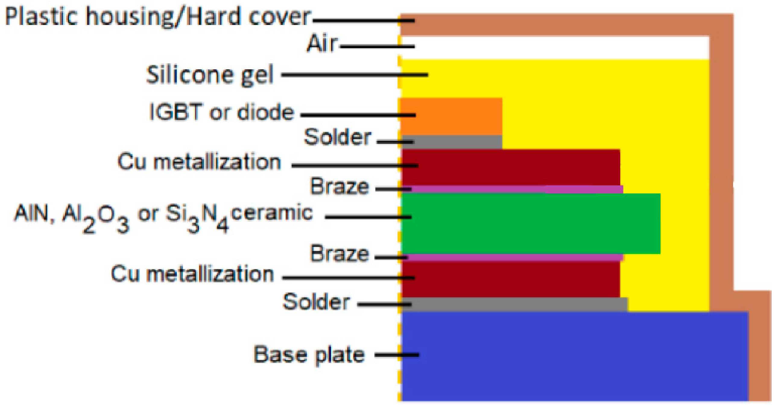
Incorporating the impact of air pressure variation into different characteristics of silicone gel and AlN, as well as the inception and extinction of the discharges.
The rest of the paper is as follows: in Section 2, the PD mechanism is reviewed, and a model is developed with the aid of finite element analysis (FEA) as a tool for the precise estimation of electric field distribution. In Section 3, the case study of this research is presented, which is an IGBT immersed in silicone gel, and a 3D model for the critical volume of this module is developed. The results of FEA modeling at two pressure levels (0.5 atm and 1 atm) are presented in this section. Finally, Section 4 concludes the paper and brings final remarks.

2. FEA Model for PD Analysis

2.1. Introduction to PD Numerical Modeling
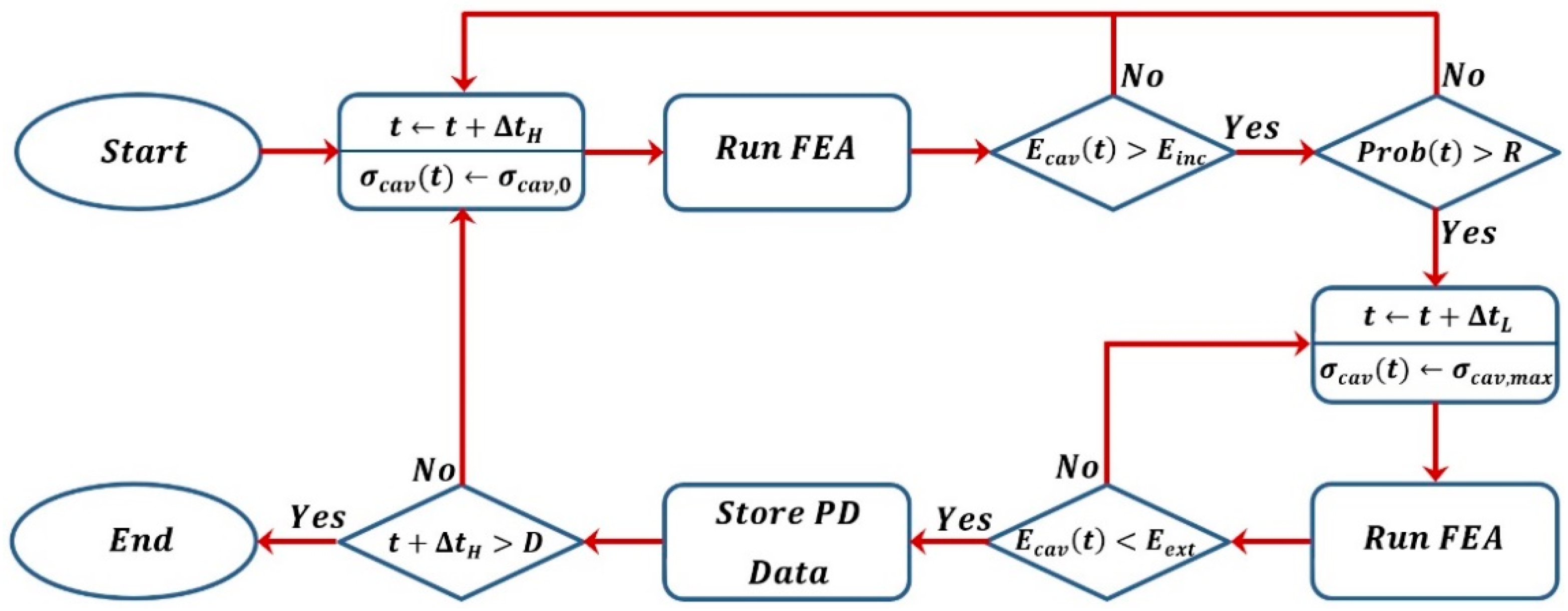
Partial discharge is a stochastic, multi-physical phenomenon, and its analysis requires a combination of programming and physical modeling of the test configuration. There are three primary PD models developed for the modeling of internal discharges: the three-capacitance (ABC) model, induced charge concept model, and numerical model.
The ABC model was first introduced by Whitehead [27] and used an equivalent circuit of the configuration. In this circuit, three capacitors represent the void, dielectric in series with the void, and the rest of the dielectric. However, this model was unable to provide valid physical insights into the PD mechanism.
In the induced charge model, the authors used the notion of induced charge on the electrode to describe the transient state of the partial discharge in the void [28,29,30]. While this model could provide a more accurate presentation of physics behind PDs, it cannot be applied to models with sophisticated geometries and extremely inhomogeneous electric field distribution.
Numerical models were founded upon methods such as FDM, FEM, and CSM to accurately obtain the distribution of electric potential and other pertinent electrical characteristics, such as electric field, field displacement, current density, etc. A method such as FEA, which was based on FEM, can effectively be applied to complicated geometries while the other two models cannot. Moreover, FEA can continuously monitor the variations of the parameters mentioned above, which provides further insights into the PD phenomenon. In the internal discharges, the presence of unwanted voids with a lower dielectric constant compared to the surrounding dielectric causes the aging mechanism. The accurate estimation of the electric field provides the basis to assess PD inception and extinction conditions and calculate the PD charge magnitude based on the current density over the electrodes and the defect surface.

2.2. Algorithm

The algorithm developed for PD modeling is demonstrated in Figure 1. The procedure starts by searching for the inception time of the first discharge. During this period, the model proceeds in time with Δ t H step and the conductivity ( σ c a v ( t ) ) of the cavity is nearly zero ( σ c a v , 0 ). The FEA model of the configuration in COMSOL Multiphysics® is then run to find the results of the Poisson and Laplace equations. This step provides the electric field distribution across the geometry (insulation and voids) helping to assess the inception time of discharge activity. The details of the parameters in the algorithm are explained in the following subsections.

2.3. Initial Electron Generation

To have an electron avalanche inside the defect, the existence of at least an initial electron is necessary. To check this condition, one should compute the rate of electron generation due to different processes. In the case of internal discharges, surface emission and volume ionization are the two dominating electron generation processes [31]:
N ˙ e , t o t ( t ) = N ˙ e , s u r f ( t ) + N ˙ e , v o l
where N ˙ e , s u r f ( t ) represents the time-variant rate of electron generation due to surface emission and N ˙ e , v o l is the constant rate of electrons produced by volume ionization. The summation of these two terms hands the total rate of electron generation, which is mainly dominated by electric field intensity in the void, and is also affected by temperature, geometry, defect, etc. The probability of initial electron provision ( P r o b ( t ) ) can be calculated with the aid of N ˙ e , t o t ( t ) :
P r o b ( t ) = 1 exp ( t P D t N ˙ e , t o t ( t ) d t )
where t P D is the time of last PD occurrence. The parameter, P r o b ( t ) , has a value between zero and unity, and its comparison with a random number in this interval determines the stochastic ignition time of partial discharge [32].

2.4. PD Inception/Extinction Criterion

Another necessary condition for the occurrence of a partial discharge is the existence of a high electric field in the proximity of the void. This allows the electrons to gain sufficient energy to collide with neutral atoms or molecules and release even more electrons. To assess this condition, a streamer inception criterion can be used to check whether the electric field inside the cavity ( E c a v ( t ) ) has exceeded the inception electric field ( E i n c ) [31]:
E i n c = ( E p ) c r p   ( 1 + B p l )    
where l and p   represent the void diameter and pressure of the gas inside it. The critical field-to-pressure ratio ( ( E / p ) c r ) and B are parameters related to the type of gas.
After the satisfaction of the two inception conditions, one needs to carefully monitor the transient state of the discharge. Therefore, a much smaller time step, Δ t L , helps not only to find the extinction time of the discharge but also obtain the amount of current flowing through the void surface and the electrodes. The extinction threshold of the partial discharge ( E e x t ) is also dependent upon the gas pressure and the critical field-to-pressure [33]:
E e x t = γ ( E / p ) c r   p            
In (4), γ is a dimensionless proportionality factor dependent upon the gas and its interface as well as the polarity of the voltage.
Another change in the transient state is the rapid rise in the cavity conductivity from nearly zero to a maximum value ( σ c a v , m a x ). This change causes a voltage (or electric field) to drop across the void. If the electric field inside the void reaches a value equal to or below E e x t , the integration of current flowing over the void between the inception and extinction time yields the apparent charge magnitude of the PD activity.
Once the transient state of a discharge terminates, the cavity conductivity and the time step return to their normal value ( σ c a v , 0 and Δ t H ) and the aforementioned process re-iterates to find the next PD event. This procedure continues until all discharges are detected in a duration of D .

3. Numerical Results

The cross-section of the IGBT module immersed in silicone gel is demonstrated in Figure 2. The main troublesome regions in this geometry are the sharp edges of the metallic electrodes. The reason lies in the high electric field intensity in the surrounding of these sharp copper edges. Hence, if there is a void in this area, a discharge can ignite and be a source of harm to the health of silicone gel as a dielectric.
For simplicity, the dies, wire bonds, and interconnections are included in this model. As mentioned in [34], the main regions under harsh electric stress are the triple joints of the metallic layers (ground and HV electrode). In these regions, the electric field can go high enough that a void in this region may be a source of aging.
The 3D model considered in this study is shown in Figure 3, and includes the AlN substrate, the ground, and the high-voltage (HV) electrode, all encapsulated in silicone gel. Since this geometry cannot be approximated by a 2D-axisymmetrical configuration, the 3D model is developed in COMSOL Multiphysics®. Note that since the dielectric material is not a sealant of the void against the external low-pressure conditions, it is assumed that the pressure of the void matches the external pressure.
The standard IEC 61287-1 lays the groundwork for the stress magnitude a module should undergo. During this test procedure, the maximum voltage applied to a system is 1.5 / 2 = 1.06 of the nominal maximum voltage (50/60 Hz sine voltage). Figure 3 demonstrates the voltage distribution when the applied voltage is V = 4.7 sin ( 100 π t ) kV (peak of the voltage).

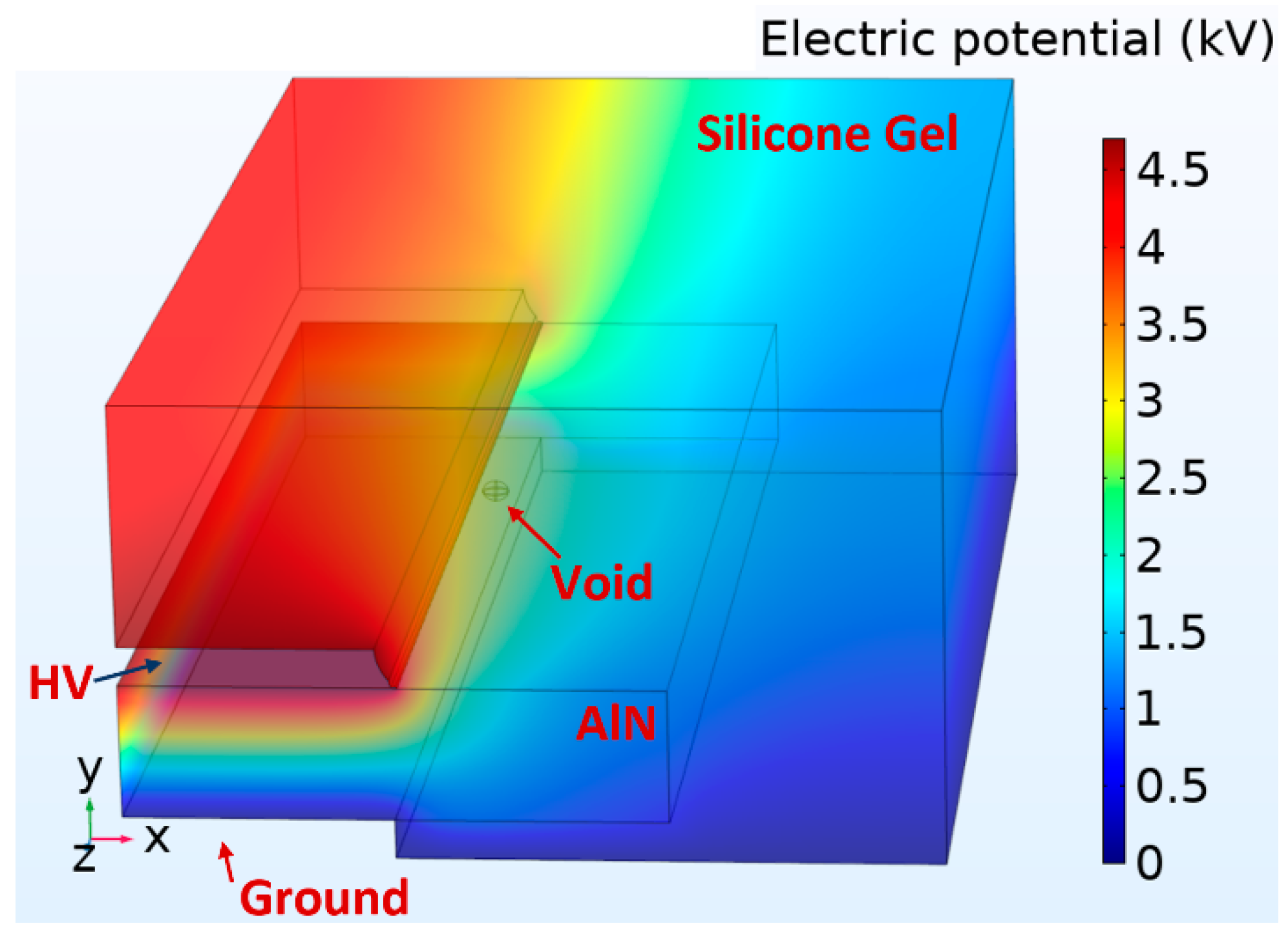
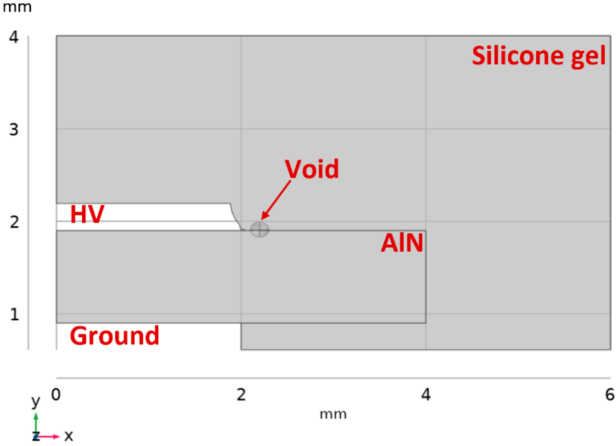
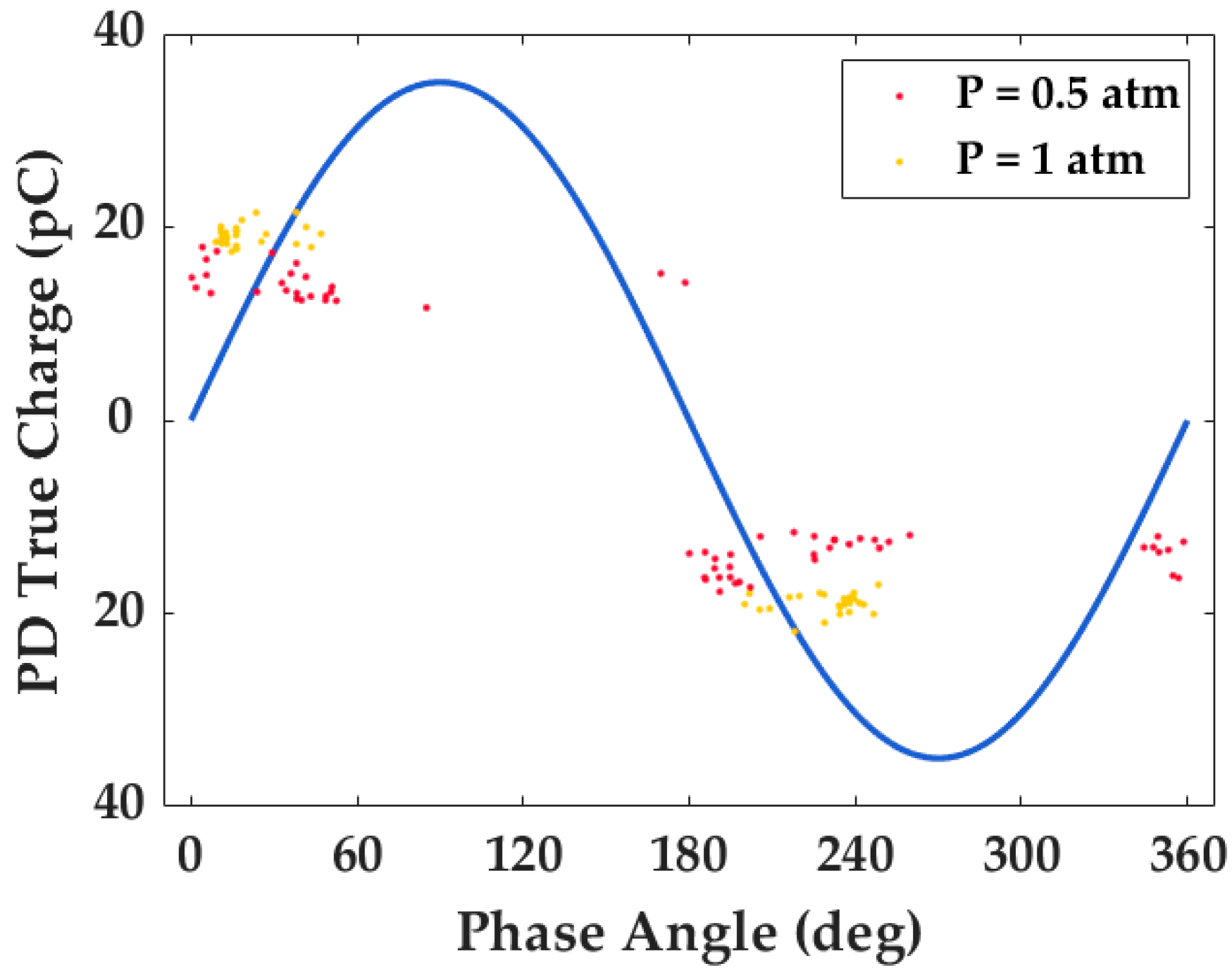
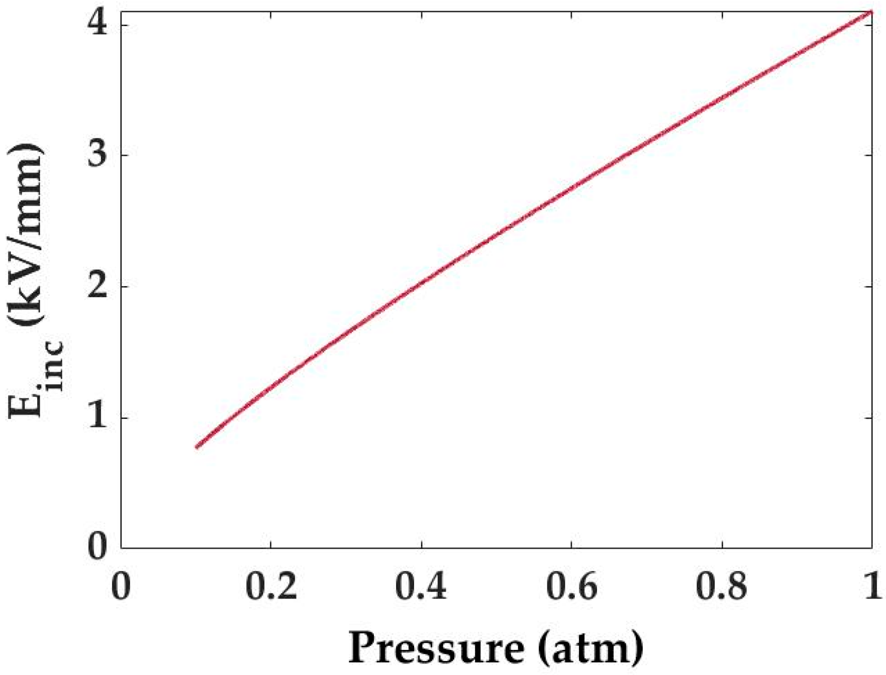
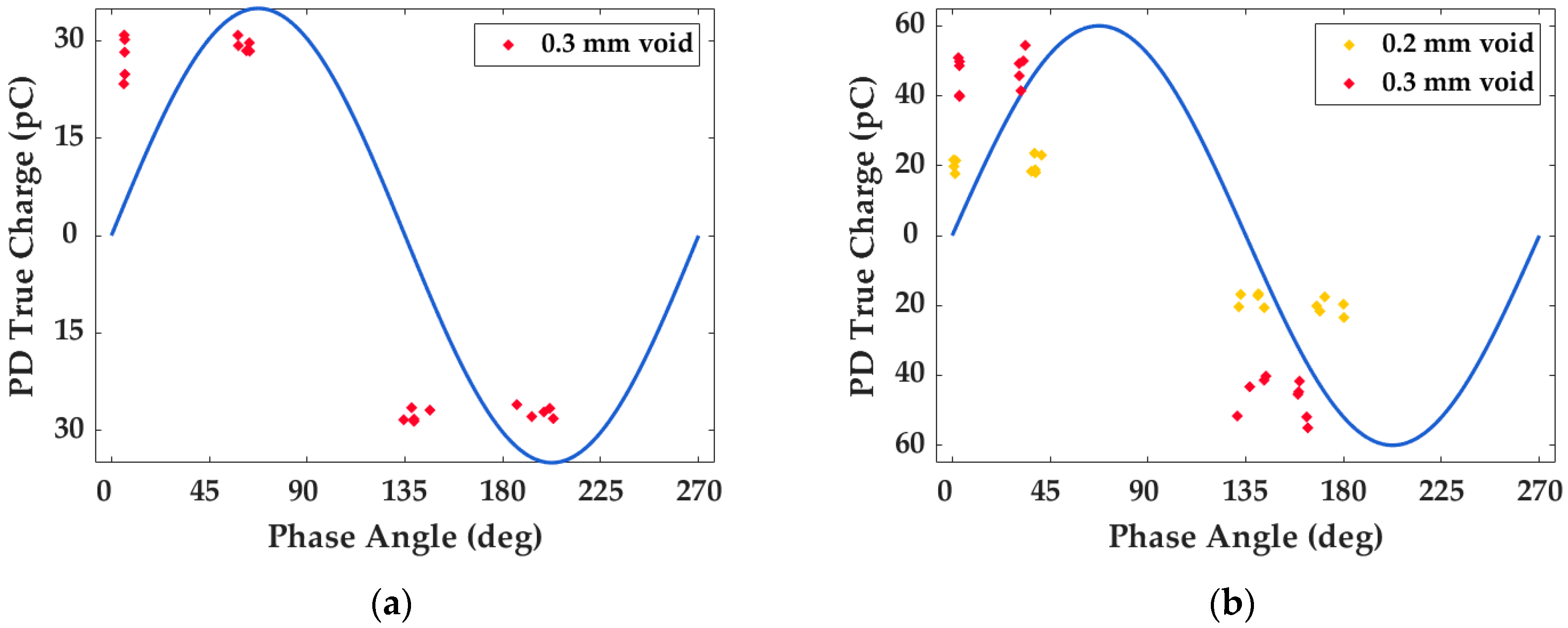
3.1. Single-Void Case Study

The 2D view of the single-void geometry is shown in Figure 4. Close to the HV copper electrode, an ellipsoidal air-filled void exists with semiaxes of ( 800   μ m ,   600   μ m ,   800   μ m ). The simulation of this case is performed for two pressure levels: 1 atm (sea level) and 0.5 atm (altitude of 18,000 ft). The PRPD pattern of this case is shown in Figure 5 (after 25 cycles of sinusoidal voltage). The y-axis of this figure is the PD true charge magnitude, which is the amount of charge accumulated over the lower surface of the void during the PD transient period. The x-axis of the figure demonstrates the voltage phase at which the PD has occurred. The statistics of PD in the single-void case are brought in Table 1. The apparent charge magnitude in Table 1 denotes the amount of charge accumulated over the surface ground electrode during the PD transient state.
At the sea level, the results show that about two discharges are detected per cycle. On the other hand, when the WBG power module works under low-pressure conditions, the discharges happen at a doubled rate. When the discharge occurs at a lower electric field (at high altitudes), the discharge tends to have a lower magnitude compared to the atmospheric environment (~26% drop). However, this does not mean that the low-pressure conditions are better in terms of PD-induced aging; as the last two rows of Table 1 show, the mean charge magnitude produced in each cycle increases at the half atmospheric pressure by about 45%.
Figure 6 demonstrates that when the pressure drops, the inception electric field will also decrease. Therefore, it takes less time to have a discharge, and the defects would have more time to generate further discharges in a single cycle of voltage. The occurrence of discharges at lower phases in Figure 5 confirms this observation.
In terms of intensity, the individual discharges produce lower charge magnitudes at high altitudes. Considering Ohm’s law ( J = σ E ), it can be justified that the breakdown of the void at lower electric fields produces a less current flow over the cavity surface. Thus, individual PDs would have lower intensity. One may argue that the same decrease occurs in the case of extinction voltage at high altitudes; the lower the pressure is, the lower E e x t will be. But it should be noted that the variation range of the extinction field is much narrower compared to the inception field. All in all, the discharges at high altitudes are lower in magnitude but higher in number.
The results after 25 cycles of PD detection can sufficiently enlighten the trend of PD behavior at the two pressure levels. However, to obtain the lifetime of a system, much longer testing is needed besides the necessity for faster processing speed and cheaper computational burden.

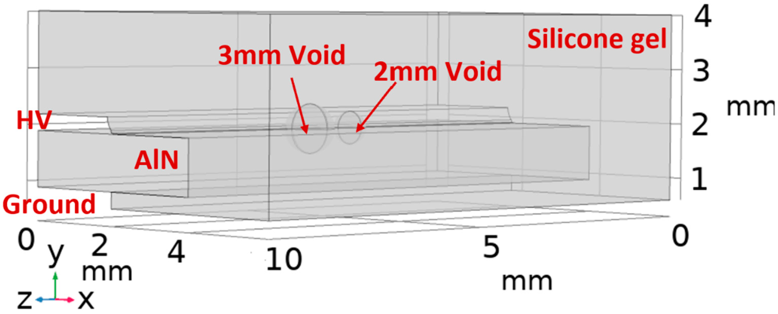
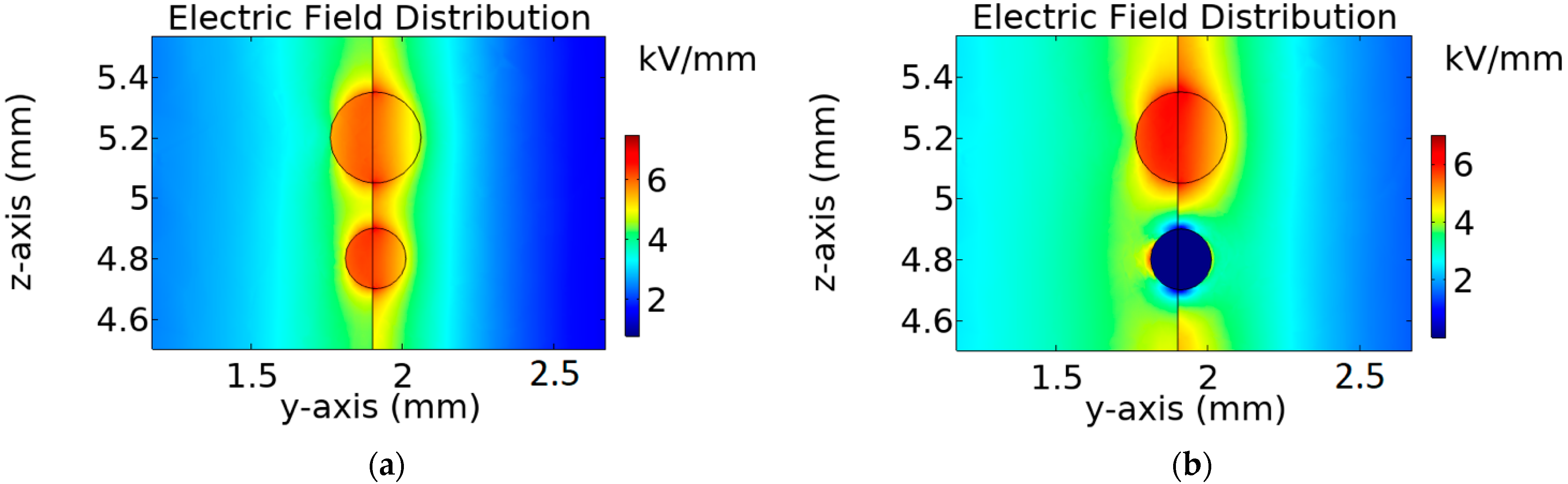
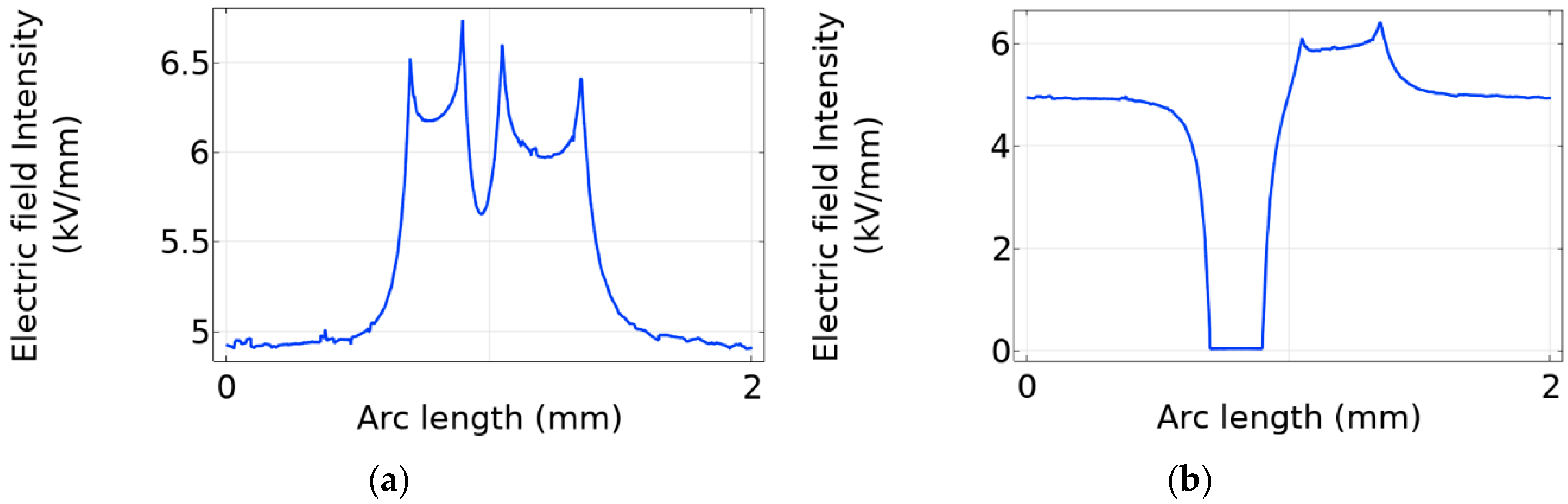
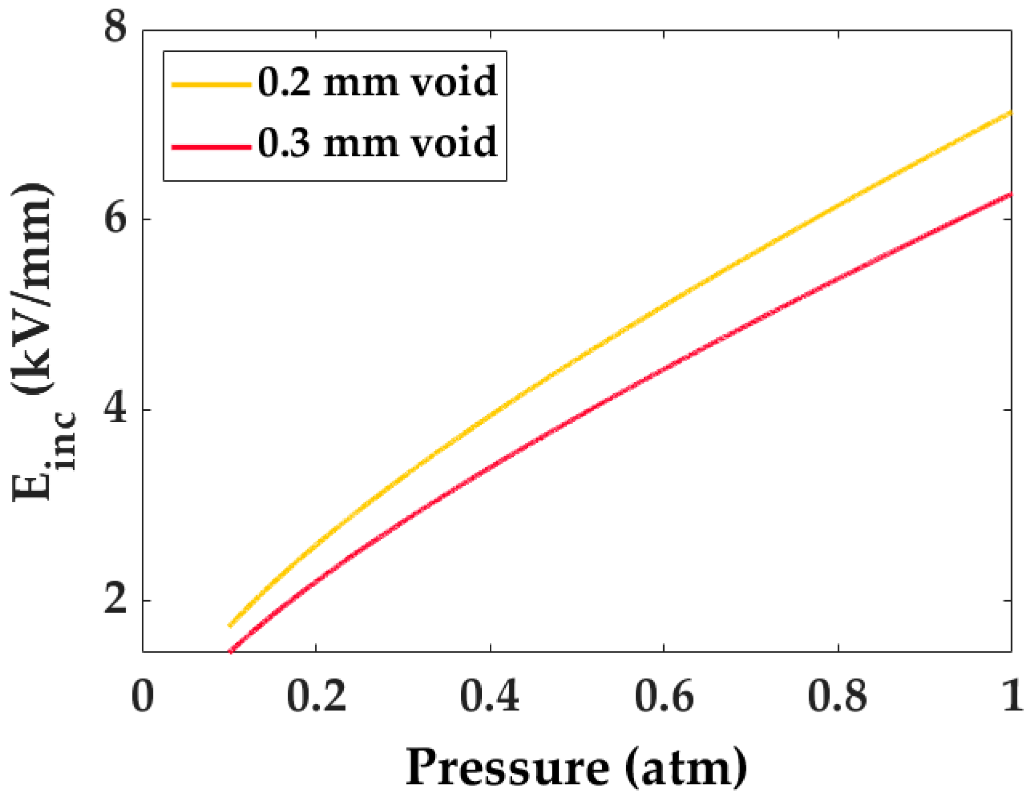
3.2. Double-Void Case Study

The existence of multiple voids in geometry makes the algorithm of PD detection more complicated. While there are only two states (PD/no PD), in the case of single-void configuration, the number of states doubles in the case of geometry with two voids. The two voids considered in this case are spherical and positioned symmetrically across the z-axis (see Figure 7). The diameter of the voids is 0.2 and 0.3 mm. In this case, it is assumed that the initial electron condition is always satisfied to remove the influence of PD’s stochasticity when comparing the two voids.
The electric field distribution across the plane that entails the cross-section of the voids is shown in Figure 8 before and after a discharge. Additionally, the electric field across the line that connects the centers of the two voids is demonstrated in Figure 9 before and after the discharge. These two figures imply that while the electric field in both voids surpasses the field in the surroundings, the larger void undergoes the highest intensity of the electric field. In addition, the inception electric field in the larger void is lower, meaning that it is more probable that discharge occurs in the larger void faster.
Figure 10 shows the distribution of discharges at two pressure levels. As can be seen in Figure 10a, PDs only occur in the larger void and no breakdown of electric field happens in the void of 0.2 mm. To investigate the reason, one can analyze the inception field of the two voids at different pressure levels. Figure 9 shows that at the atmospheric pressure, E i n c for the voids of 0.2 and 0.3 mm is 7.14 kV/mm and 6.28 kV/mm, respectively. Since the electric field in the smaller void does not exceed the corresponding threshold, no discharge occurs there.
However, the situation differs when operating at a higher altitude where the pressure drops to 0.5   atm . As seen in Figure 10b and Table 2, not only does the number of discharges increase at the lower pressure level but also the smaller void becomes a medium for discharge. As seen in Figure 11, the inception electric field at P = 0.5   atm reduces by 36.4% and 37.4% in the 0.2 and 0.3 voids, respectively. Therefore, the electric field can more quickly cause the breakdown in internal voids at lower pressure.
The study of multiple voids shows that the multitude of different voids, even smaller ones, adversely affect the aging of the dielectric. In the case of the larger void, the rate of PD occurrence at the atmospheric pressure and sub-atmospheric pressure is the same. However, the magnitude of discharges under low-pressure conditions increases. The coupling of discharges between the two voids affects the discharge magnitudes observed at the voids’ surface and electrodes. This results in a more than 66% increase in the true charge magnitude at half atmospheric pressure.
On the other hand, the smaller void with a 0.2 mm diameter does not show any discharge at atmospheric pressure while with the decrease in E i n c at low pressures, the void starts to show PD activities as well. In this example of two voids, at P = 0.5   atm , the intensity of PD activities is more than twice the intensity of PDs at P = 1   atm . The comparison of the single-void and the double-void cases shows that the impact of low-pressure conditions is not easy to predict even with well-known theories such as Paschen law. The microscopic defects during the manufacturing process can be more devastating than expected.

4. Conclusions

One of the main obstacles in the path toward electrification is the adverse impact of harsh environmental conditions. In the example of a high-altitude condition, lower air pressure accelerates the aging of insulating materials due to partial discharges. This paper puts forth an approach to model the PD behavior in an IGBT module under two conditions: (1) Sea level (atmospheric pressure) and (2) Altitude of 18,000 ft. (half atmospheric pressure). A numerical model using FEA is developed to detect the discharges in the silicone gel encapsulant of a WBG-based IGBT module according to the standard IEC 61287-1. In one of the case studies, the existence of a single void close to the triple joint of the HV electrode causes PD occurrence in both pressure levels. However, at the lower pressure level, the rate of PD occurrence doubles, and although the intensity of individual PDs decreases, the total amount of produced charge per cycle increases by more than 40%. In the double-void case, the coupling of two voids could be devastating at the cruising altitude and increase the PD intensity by more than 100% compared to the sea-level pressure.
Future studies will focus on the generalization of the PD model based on the image of the dielectric defects. This requires overcoming computational challenges as real-cases demand 3D models while having very fine meshes in regions with high electric tension. The studies presented in this paper can be a foundation to build an online condition monitoring system to determine the extent and severity of internal defects in insulation systems. Measuring PRPD patterns and using our PD model, we may predict the voids’ dimension, number, and location.

Author Contributions

The authors contributed equally to this work in all parts. Both authors have read and agreed to the published version of the manuscript.

Funding

This work was supported in part by the Air Force Office of Scientific Research under Award FA9550-20-1-033.

Data Availability Statement

Not applicable.

Conflicts of Interest

The authors declare no conflict of interest.

Abbreviations

AlNAluminum Nitride
CO2Carbon Dioxide
CSMCharge Simulation Method
FDMFinite Difference Method
FEAFinite Element Analysis
FEMFinite Element Method
GHGGreenhouse Gases
HVHigh Voltage
IGBTInsulated Gate Bipolar Transistor
PCBPrinted Circuit Board
PIPolyimide
PDPartial Discharge
PDIVPartial Discharge Inception Voltage
PRPDPhase-Resolved Partial Discharge
WBGWide Bandgap

References

  1. IPCC. Summary for Policymakers. In Climate Change 2021: The Physical Science Basis. Contribution of Working Group I to the Sixth Assessment Report of the Intergovernmental Panel on Climate Change; Masson Delmotte, V., Zhai, P., Pirani, A., Connors, S.L., Péan, C., Berger, S., Caud, N., Chen, Y., Goldfarb, L., Gomis, M.I., et al., Eds.; Cambridge University Press: Cambridge, UK, 2021; in press. [Google Scholar]
  2. Wolf, S.; Teitge, J.; Mielke, J.; Schütze, F.; Jaeger, C. The European Green Deal—More Than Climate Neutrality. Intereconomics 2021, 56, 99–107. [Google Scholar] [CrossRef] [PubMed]
  3. Traffic Data for U.S. Airlines and Foreign Airlines U.S. Flights. Bureau of Transportation Statistics, United States Department of Transportation. Available online: https://www.bts.gov/statistical-releases (accessed on 12 August 2020).
  4. Soloveichik, G. Electrified Future of Aviation: Batteries or Fuel Cells? The Advanced Research Projects Agency–Energy (ARPA-E): Washington, DC, USA, 2019. [Google Scholar]
  5. Barzkar, A.; Ghassemi, M. Electric Power Systems in More and All Electric Aircraft: A Review. IEEE Access 2020, 8, 169314–169332. [Google Scholar] [CrossRef]
  6. Liu, X.; Furrer, D.; Kosters, J.; Holmes, J. Vision 2040: A Roadmap for Integrated, Multiscale Modeling and Simulation of Materials and Systems; Tech. Rep. NASA/CR-2018-219771; NASA: Cleveland, OH, USA, March 2018. [Google Scholar]
  7. Borghei, M.; Ghassemi, M. Insulation Materials and Systems for More- and All-Electric Aircraft: A Review Identifying Challenges and Future Research Needs. IEEE Trans. Transp. Electrif. 2021, 7, 1930–1953. [Google Scholar] [CrossRef]
  8. Yongxing, W.; Enyuan, D.; Jiyuan, C.; Jiyan, Z.; Koenig, D. Arc Tracking Properties of the Aging Wires in Aircraft. In Proceedings of the 2008 2nd International Symposium on Systems and Control in Aerospace and Astronautics, Shenzhen, China, 10–12 December 2008; pp. 462–466. [Google Scholar] [CrossRef]
  9. Riba, J.-R.; Gómez-Pau, Á.; Moreno-Eguilaz, M.; Bogarra, S. Arc Tracking Control in Insulation Systems for Aeronautic Applications: Challenges, Opportunities, and Research Needs. Sensors 2020, 20, 1654. [Google Scholar] [CrossRef] [PubMed] [Green Version]
  10. Hillard, G.B.; Kirkici, H. High Voltage Design Guidelines: A Timely Update. In Proceedings of the 2001 Annual Report Conference on Electrical Insulation and Dielectric Phenomena (Cat. No.01CH37225), Kitchener, ON, Canada, 14–17 October 2001; pp. 409–411. [Google Scholar] [CrossRef] [Green Version]
  11. Kaplar, R.J.; Neely, J.C.; Huber, D.L.; Rashkin, L.J. Generation-After-Next Power Electronics: Ultrawide-Bandgap Devices, High-Temperature Packaging, and Magnetic Nanocomposite Materials. IEEE Power Electron. Mag. 2017, 4, 36–42. [Google Scholar] [CrossRef]
  12. Wang, P.; Cavallini, A.; Montanari, G.C. The Influence of Repetitive Square Wave Voltage Parameters on Enameled Wire Endurance. IEEE Trans. Dielectr. Electr. Insul. 2014, 21, 1276–1284. [Google Scholar] [CrossRef]
  13. Wang, P.; Cavallini, A.; Montanari, G.C.; Wu, G. Effect of Rise Time on PD Pulse Features under Repetitive Square Wave Voltages. IEEE Trans. Dielectr. Electr. Insul. 2013, 20, 245–254. [Google Scholar] [CrossRef]
  14. Borghei, M.; Ghassemi, M. Partial discharge finite element analysis under fast, repetitive voltage pulses. In Proceedings of the 2019 IEEE Electric Ship Technologies Symposium (ESTS), Washington, DC, USA, 14–16 August 2019; pp. 324–328. [Google Scholar] [CrossRef]
  15. Ghassemi, M. Geometrical techniques for electric field control in (ultra) wide bandgap power electronics modules. In Proceedings of the 2018 IEEE Electrical Insulation Conference (EIC), San Antonio, TX, USA, 17–20 June 2018; pp. 589–592. [Google Scholar] [CrossRef]
  16. Tousi, M.M.; Ghassemi, M. Combined Geometrical Techniques and Applying Nonlinear Field Dependent Conductivity Layers to Address the High Electric Field Stress Issue in High Voltage High-Density Wide Bandgap Power Modules. IEEE Trans. Dielectr. Electr. Insul. 2020, 27, 305–313. [Google Scholar] [CrossRef]
  17. Tousi, M.M.; Ghassemi, M. Characterization of Nonlinear Field Dependent Conductivity Layer Coupled with Protruding Substrate to Address High Electric Field Issue within High Voltage High-Density Wide Bandgap Power Modules. IEEE J. Emerg. Sel. Top. Power Electron. 2020, 8, 343–350. [Google Scholar] [CrossRef]
  18. Wang, N.; Cotton, I.; Robertson, J.; Follmann, S.; Evans, K.; Newcombe, D. Partial Discharge Control in a Power Electronic Module Using High Permittivity Non-Linear Dielectrics. IEEE Trans. Dielectr. Electr. Insul. 2010, 17, 1319–1326. [Google Scholar] [CrossRef]
  19. Fang, L.; Cotton, I.; Wang, Z.J.; Freer, R. Insulation Performance Evaluation of High Temperature Wire Candidates for Aerospace Electrical Machine Winding Application. In Proceedings of the 2013 IEEE Electrical Insulation Conference (EIC), Ottawa, ON, Canada, 2–5 June 2013; pp. 253–256. [Google Scholar] [CrossRef]
  20. Gardner, R.; Cotton, I.; Emersic, C.; Rowland, S.; Freer, R. Thermal Stresses of Conformal Coating on Printed Circuit Boards. In Proceedings of the 2015 IEEE Electrical Insulation Conference (EIC), Seattle, WA, USA, 7–10 June 2015; pp. 106–109. [Google Scholar] [CrossRef]
  21. Meyer, D.R.; Cavallini, A.; Lusuardi, L.; Barater, D.; Pietrini, G.; Soldati, A. Influence of Impulse Voltage Repetition Frequency on RPDIV in Partial Vacuum. IEEE Trans. Dielectr. Electr. Insul. 2018, 25, 873–882. [Google Scholar] [CrossRef]
  22. Bayer, C.F.; Baer, E.; Waltrich, U.; Malipaard, D.; Schletz, A. Simulation of the electric field strength in the vicinity of metallization edges on dielectric substrates. IEEE Trans. Dielectr. Electr. Insul. 2015, 22, 257–265. [Google Scholar] [CrossRef]
  23. Bayer, C.F.; Waltrich, U.; Soueidan, A.; Baer, E.; Schletz, A. Partial discharges in ceramic substrates—Correlation of electric field strength simulations with phase resolved partial discharge measurements. In Proceedings of the 2016 International Conference on Electronics Packaging (ICEP), Hokkaido, Japan, 20–22 April 2016; pp. 530–535. [Google Scholar] [CrossRef]
  24. Borghei, M.; Ghassemi, M. Partial Discharge Analysis under High-Frequency, Fast-Rise Square Wave Voltages in Silicone Gel: A Modeling Approach. Energies 2019, 12, 4543. [Google Scholar] [CrossRef] [Green Version]
  25. Borghei, M.; Ghassemi, M. Finite element modeling of partial discharge activity within a spherical cavity in a solid dielectric material under fast, repetitive voltage pulses. In Proceedings of the 2019 IEEE Electrical Insulation Conference (EIC), Calgary, AB, Canada, 16–19 June 2019; pp. 34–37. [Google Scholar] [CrossRef]
  26. Borghei, M.; Ghassemi, M. A Finite Element Analysis Model for Partial Discharges in Silicone Gel under a High Slew Rate, High-Frequency Square Wave Voltage in Low-Pressure Conditions. Energies 2020, 13, 2152. [Google Scholar] [CrossRef]
  27. Whitehead, S. Dielectric Breakdown in Solids; Clarendon Press: Oxford, UK, 1951. [Google Scholar]
  28. Crichton, G.C.; Karlsson, P.W.; Pedersen, A. Partial Discharges in Ellipsoidal and Spheroidal Voids. IEEE Trans. Electr. Insul. 1989, 24, 335–342. [Google Scholar] [CrossRef] [Green Version]
  29. Pedersen, A.; Crichton, G.C.; McAllister, I.W. The Theory and Measurement of Partial Discharge Transients. IEEE Trans. Electr. Insul. 1991, 26, 487–497. [Google Scholar] [CrossRef] [Green Version]
  30. Pedersen, A.; Crichton, G.C.; McAllister, I.W. The Functional Relation between Partial Discharges and Induced Charge. IEEE Trans. Dielectr. Electr. Insul. 1995, 2, 535–543. [Google Scholar] [CrossRef] [Green Version]
  31. Niemeyer, L. A Generalized Approach to Partial Discharge Modeling. IEEE Trans. Dielectr. Electr. Insul. 1995, 2, 510–528. [Google Scholar] [CrossRef] [Green Version]
  32. Forssen, C.; Edin, H. Partial Discharges in a Cavity at Variable Applied Frequency Part 2: Measurements and Modeling. IEEE Trans. Dielectr. Electr. Insul. 2008, 15, 1610–1616. [Google Scholar] [CrossRef]
  33. Gutfleisch, F.; Niemeyer, L. Measurement and Simulation of PD in Epoxy Voids. IEEE Trans. Dielectr. Electr. Insul. 1995, 2, 729–743. [Google Scholar] [CrossRef]
  34. Ghassemi, M. PD Measurements, Failure Analysis, and Control in High-Power IGBT Modules. High Volt. 2018, 3, 170–178. [Google Scholar] [CrossRef]
Figure 1. The PD simulation flowchart.
Energies 14 05394 g001
Figure 2. Schematic layers of IGBT module.
Energies 14 05394 g002
Figure 3. The 3D representation of the geometry used for simulation.
Energies 14 05394 g003
Figure 4. The 2D view of the single-void geometry.
Energies 14 05394 g004
Figure 5. PRPD pattern based on true charge magnitude.
Energies 14 05394 g005
Figure 6. The inception electric field versus pressure for an ellipsoidaland void with 800   μ m radius in electric field direction.
Energies 14 05394 g006
Figure 7. The 3D view of the double-void geometry.
Energies 14 05394 g007
Figure 8. The electric field distribution across the voids’ cross-section (a) before and (b) after PD occurrence.
Energies 14 05394 g008
Figure 9. The electric field distribution across the line that connects the voids’ centers (a) before and (b) after PD occurrence.
Energies 14 05394 g009
Figure 10. The phase-resolved PD pattern for (a) P = 1   atm and (b) P = 0.5   atm .
Energies 14 05394 g010
Figure 11. The inception electric field of the two voids versus pressure.
Energies 14 05394 g011
Table 1. Comparison of PD characteristics in the single-void case.
Quantity P   =   0.5   a t m P   =   1   a t m
Number of PDs per Cycle 3.98 2.03
Mean True Charge 14.14   pC 19.08   pC
Mean Apparent Charge 2.24   pC 2.78   pC
Maximum True Charge 17.74   pC 21.87   pC
Maximum Apparent Charge 3.42   pC 4.00   pC
Mean True Charge per Cycle 56.28   pC 38.67   pC
Mean Apparent Charge per Cycle 8.95   pC 5.63   pC
Table 2. Comparison of PD characteristics in the double-void case.
Quantity P   =   0.5   a t m P   =   1   a t m
0.2 mm Void0.3 mm Void0.2 mm Void0.3 mm Void
Number of PDs per Cycle4.003.80 03.80
Mean True Charge19.73 pC 46.82 pC -28.06 pC
Mean Apparent Charge3.15 pC 8.68 pC -3.93 pC
Maximum True Charge20.69 pC 48.82 pC -29.27 pC
Maximum Apparent Charge3.37 pC 9.19 pC -4.38 pC
Total True Charge per Cycle 78.84 pC 177.74 pC -106.82 pC
Total Apparent Charge per Cycle 12.60 pC 32.96 pC -14.85 pC
Publisher’s Note: MDPI stays neutral with regard to jurisdictional claims in published maps and institutional affiliations.

