Article

A Modified Grid-Connected Inverter Topology for Power Oscillation Suppression under Unbalanced Grid Voltage Faults

1
State Key Laboratory of Electrical Insulation and Power Equipment, School of Electrical Engineering, Xi’an Jiaotong University, Xi’an 710049, China
2
Xi’an XD Power System Co., Ltd., Xi’an 710075, China
*
Author to whom correspondence should be addressed.
Energies 2021, 14(16), 5057; https://doi.org/10.3390/en14165057
Submission received: 18 July 2021 / Revised: 6 August 2021 / Accepted: 15 August 2021 / Published: 17 August 2021
(This article belongs to the Topic Application of Innovative Power Electronic Technologies)

Abstract

:
Under unbalanced grid voltage faults, the output power oscillation of a grid-connected inverter is an urgent problem to be solved. In the traditional topology of inverters, it is impossible to eliminate power oscillation and simultaneously maintain balanced output current waveform. In this paper, considering the solvability of reference current matrix equation, the inherent mechanism of inverter output power oscillation is analyzed, and a modified topology with auxiliary modules inserted in series between the inverter output filter and the point of common coupling (PCC) is proposed. Due to the extra controllable freedoms provided by auxiliary modules, the inverter could generate extra voltage to correct PCC voltage while keeping balance of output current, so as to eliminate the oscillation of output power. Simulation and experimental results verify the effectiveness of the proposed topology.

1. Introduction

The grid-connected inverter is the vital interface module for distributed generation (DG) systems, including wind power generation, photovoltaic power generation, to be connected to the grid. It can directly determine the value and direction of current and power and is crucial for the safe operation of the grid [1,2]. Small and medium-sized DG systems are often connected to the grid through the power distribution network. However, due to the abnormal weather conditions, large load switching on–off, insulation failure, human error and so on, voltage faults often occur in the power distribution network. Most of voltage faults can be attributed to the asymmetric faults of grid voltage, for example, the unbalanced voltage fault caused by single-phase grounding is a representative type [3]. In the case of asymmetric faults, the grid-connected inverter is required to have the low voltage ride through (LVRT) capability so as to avoid the chain reaction of DGs disconnection with the grid [4,5]. When the voltage at the point of common coupling (PCC) drops, grid code requires the inverter to keep connecting with the grid for a certain period of time [3]. At the same time, the grid-connected inverter should have the power transmission capacity under abnormal voltage at PCC [1,6]. Under unbalanced PCC voltage, the traditional current closed-loop control strategy which only controls positive-sequence current in essence will cause output power oscillation so as to enlarge the voltage ripple of DC side bus and damage the output current quality [6,7,8,9]. To enhance the performance of inverters, it is necessary to eliminate the output power oscillation of grid-connected inverters under unbalanced PCC voltage.
At present, the main methods to eliminate the output power oscillation of grid-connected inverter under unbalanced grid voltage can be divided into two categories: the first type is to improve the control strategy; the second one is to change the topology of the inverter. In [6,10,11], different proportions of negative-sequence current is added to the current reference to decrease power oscillation. The main problem is that the output current has difficulty meeting the requirements of grid codes, and there may be risk of current overrun. In [12,13], the power reference is modified by considering the upper current limit value of switch tube to guarantee that the output current will not exceed the maximum allowable value. However, the waveform of the output current is seriously distorted. A positive and negative-sequence conductance and susceptance control scheme is proposed in [14]. By optimizing the value of negative-sequence conductance, the peak value of the output current can be controlled, but the power oscillation is not effectively reduced. The second type of strategy is to eliminate the power oscillation by changing the topology of the inverter. In [15], a three-phase four-wire system with zero-sequence current channel is proposed. The introduction of zero-sequence current increases the controllable quantity of the system, which is conducive to eliminating power oscillation and improving current quality. Nevertheless, the power oscillation still exists when adopting the current closed-loop control strategy. In one word, the reference current matrix equation of grid-connected inverter in the topologies mentioned above cannot meet the solvability condition, which is the essential reason that the power oscillation could not be eliminated while the current waveform is balanced.
In this paper, a modified grid-connected inverter topology with auxiliary modules inserted in series between PCC and the output filter of each phase is proposed, which could increase the controllable freedoms of reference current equation of inverter so as to make the reference current equation of the inverter meet the solvability condition. Then, the oscillation of the output power is eliminated, and the negative-sequence current is avoided to be injected into power grid simultaneously. The simulation and experimental results are presented to verify the effectiveness of the modified topology.

2. Relationship between Power Oscillation and Grid Voltage in Traditional Topology

Typical grid voltage faults can be divided into seven categories [16], most of them are asymmetric faults. Unbalanced voltage fault caused by single-phase grounding is a representative one [3]. The unbalanced voltage at PCC will cause the oscillation of output power and the distortion of output current, which will affect the safe operation of the grid-connected inverters [11].

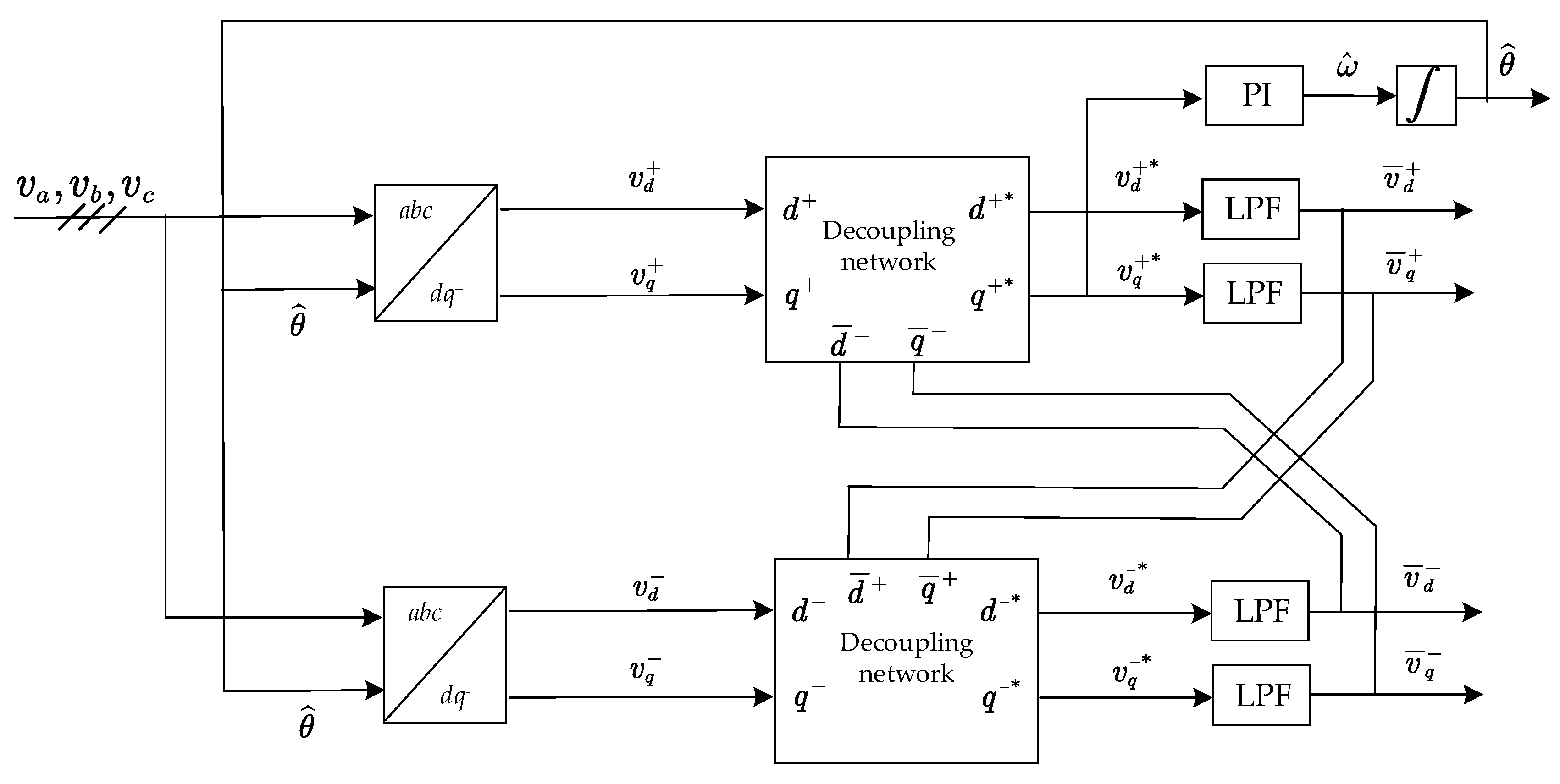
2.1. Relationship among Output Current, Power Oscillation and Unbalanced Voltage
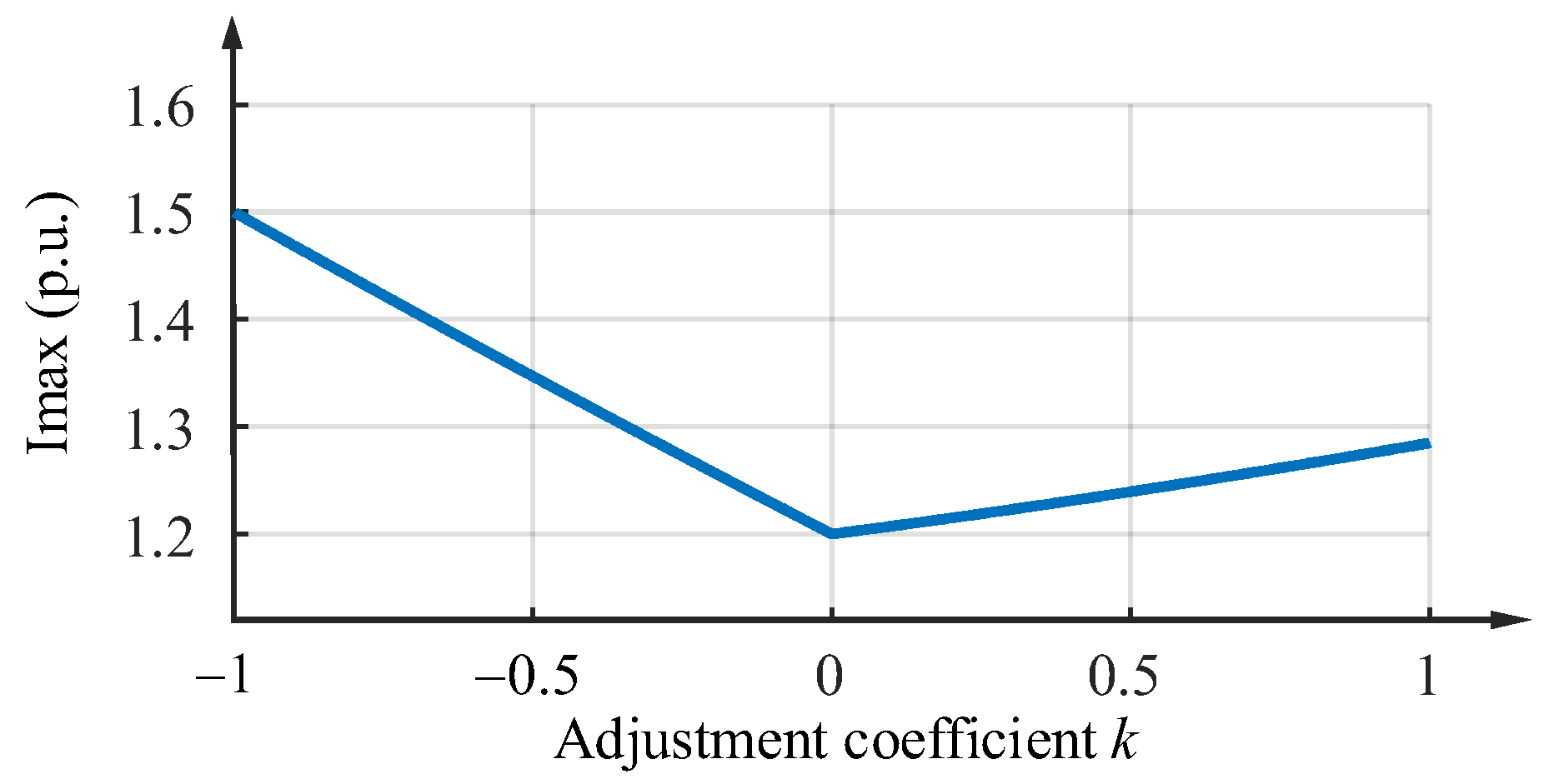
The traditional control strategy of grid-connected inverters under unbalanced grid voltage can be summarized as a unified control strategy [10,11,17], which uses different values of adjustment coefficient ( 1 k 1 ) to reflect different control strategies, as shown in Table 1. No matter what control strategy is used, it is always difficult to achieve the optimal output current and power at the same time. A quantitative numerical analysis is given as follows.
(1).
Numerical analysis of output current
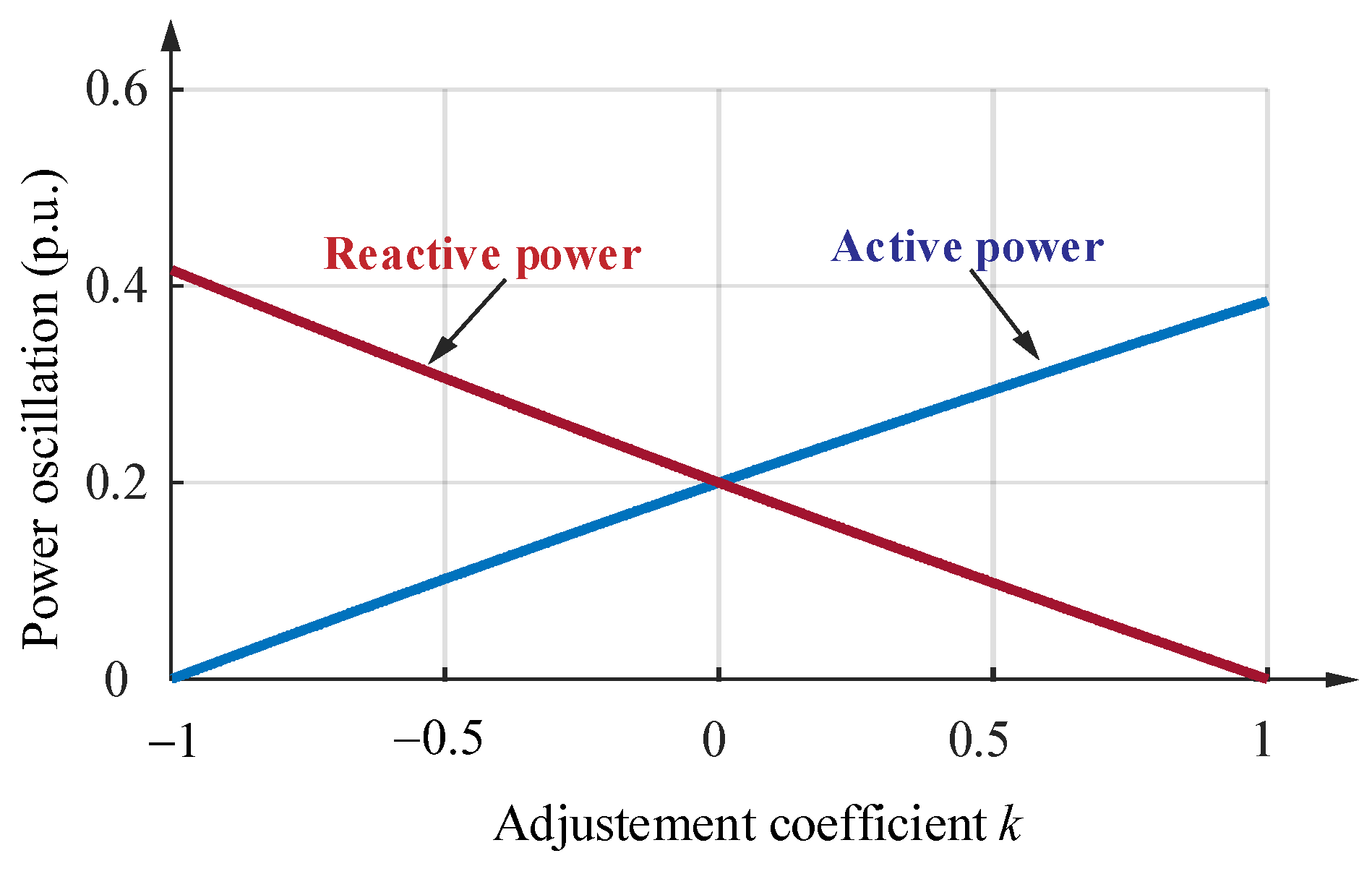
Since there is no zero-sequence current component channel in the three-phase three-wire power distribution network, the voltage at PCC and output current can be expressed in Equation (1):
[ u a u b u c ] = U + [ sin ( ω t + θ v p ) sin ( ω t + θ v p 120 ° ) sin ( ω t + θ v p + 120 ° ) ] + U [ sin ( ω t + θ v n ) sin ( ω t + θ v n + 120 ° ) sin ( ω t + θ v n 120 ° ) ] + U 0 [ sin ( ω t + θ 0 ) sin ( ω t + θ 0 ) sin ( ω t + θ 0 ) ]
[ i a i b i c ] = I + [ sin ( ω t + θ i p ) sin ( ω t + θ i p 120 ° ) sin ( ω t + θ i p + 120 ° ) ] + I [ sin ( ω t + θ i n ) sin ( ω t + θ i n + 120 ° ) sin ( ω t + θ i n 120 ° ) ]
where U + , U and U 0 are the amplitudes of positive, negative and zero-sequence components of the voltage, I+ and I are the amplitudes of positive and negative-sequence components of output current, θvp, θvn and θ0 are the initial phase angles of positive, negative and zero-seqence components of the voltage, θip and θin are the initial phase angles of positive, negative-sequence component of output current and ω is the angular frequency of the voltage, respectively.
When the three-phase inverter is connected to the grid, the current reference value is shown in Equations (3) and (4) [12].
I α * = 2 3 P * ( U + ) 2 + k ( U ) 2 [ U + sin ( ω t + θ v p ) + k U sin ( ω t + θ v n ) ] + 2 3 Q * ( U + ) 2 + k ( U ) 2 [ U + cos ( ω t + θ v p ) k U cos ( ω t + θ v n ) ]
I β * = 2 3 P * ( U + ) 2 + k ( U ) 2 [ U + cos ( ω t + θ v p ) + k U cos ( ω t + θ v n ) ] + 2 3 Q * ( U + ) 2 k ( U ) 2 [ U + sin ( ω t + θ v p ) + k U sin ( ω t + θ v n ) ]
where P* and Q* are the reference values of active power and reactive power, respectively.
After transformation to abc coordinate system, Equations (5)–(7) are obtained,
I a * = 2 3 A 1 2 + ( k A 2 ) 2 + 2 k A 1 A 2 cos ( θ v p θ v n 2 δ ) sin ( ω t + ψ a )
I b * = 2 3 A 1 2 + ( k A 2 ) 2 + 2 k A 1 A 2 cos ( θ v p θ v n 2 δ 240 ° ) sin ( ω t + ψ b )
I c * = 2 3 A 1 2 + ( k A 2 ) 2 + 2 k A 1 A 2 cos ( θ v p θ v n 2 δ + 240 ° ) sin ( ω t + ψ c )
where,
A 1 = [ P * U + ( U + ) 2 + k ( U ) 2 ] 2 + [ Q * U + ( U + ) 2 k ( U ) 2 ] 2
δ = arctan Q * [ ( U + ) 2 + k ( U ) 2 ] P * [ ( U + ) 2 k ( U ) 2 ]
A 2 = [ P * U ( U + ) 2 + k ( U ) 2 ] 2 + [ Q * U ( U + ) 2 k ( U ) 2 ] 2
ψ a = arctan A 1 sin ( θ v p δ ) + k A 2 sin ( θ v n δ ) A 1 cos ( θ v p δ ) + k A 2 cos ( θ v n δ )
ψ b = arctan A 1 sin ( θ v p δ 120 ° ) + k A 2 sin ( θ v n δ + 120 ° ) A 1 cos ( θ v p δ 120 ° ) + k A 2 cos ( θ v n δ + 120 ° )
ψ c = arctan A 1 sin ( θ v p δ + 120 ° ) + k A 2 sin ( θ v n δ 120 ° ) A 1 cos ( θ v p δ + 120 ° ) + k A 2 cos ( θ v n δ 120 ° ) .
When three-phase inverter is in grid-connected operation state, the current closed-loop control strategy is often used [8], so the output current could accurately track the reference value. The maximum value of output current is given as Equation (8):
I max = max { 2 3 A 1 2 + ( k A 2 ) 2 + 2 k A 1 A 2 cos ( θ p θ n 2 δ ) , 2 3 A 1 2 + ( k A 2 ) 2 + 2 k A 1 A 2 cos ( θ p θ n 2 δ 240 ° ) , 2 3 A 1 2 + ( k A 2 ) 2 + 2 k A 1 A 2 cos ( θ p θ n 2 δ + 240 ° ) } .
It can be seen from Equations (5)–(7) that the amplitudes and phase angles of three-phase currents are related to the amplitudes of positive and negative-sequence voltages, initial phase angles of positive and negative-sequence voltages, power reference value and adjustment coefficient k. To ensure that the output current of grid-connected inverters meets the grid codes [18,19], the only way is to set the adjustment coefficient k as 0, which means to use the balanced positive sequence control (BPSC) strategy [20].
According to Equation (8), when the parameters of Table 2 are adopted, the relationship between the maximum value of output current amplitude and the adjustment coefficient k is shown in Figure 1. When k changes from 1 to 1, the maximum value of output current amplitude decreases firstly and then increases, and the BPSC control method, which means k as 0, can ensure that the current stress of the inverter is minimum under the same power.
(2).
Analysis of power oscillation
According to the instantaneous power theory, the active power and reactive power can be expressed as Equations (9) and (10):
p = 3 2 u α [ A 1 sin ( ω t + θ v p δ ) + k A 2 sin ( ω t + θ v n δ ) ] + 3 2 u β [ A 1 cos ( ω t + θ v p δ ) + k A 2 cos ( ω t + θ v n δ ) ]
q = 3 2 u α [ A 1 cos ( ω t + θ v p δ ) + k A 2 cos ( ω t + θ v n δ ) ] + 3 2 u β [ A 1 sin ( ω t + θ v p δ ) + k A 2 sin ( ω t + θ v n δ ) ]
where uα and uβ are the αβ axis components of the PCC voltage, respectively.
When expanding Equations (9) and (10), the quadratic term is the fluctuating power, as shown in Equations (11) and (12):
Δ p = ( 1 + k ) P * ( U + ) 2 + k ( U ) 2 U + U cos ( 2 ω t + θ v p + θ v n ) ( 1 + k ) Q * ( U + ) 2 k ( U ) 2 U + U sin ( 2 ω t + θ v p + θ v n )
Δ q = ( 1 k ) P * ( U + ) 2 + k ( U ) 2 U + U sin ( 2 ω t + θ v p + θ v n ) ( 1 k ) Q * ( U + ) 2 k ( U ) 2 U + U cos ( 2 ω t + θ v p + θ v n ) .
When the parameters shown in Table 2 are adopted, the relationship between the power oscillation value and the adjustment coefficient k is shown in Figure 2. When k changes from −1 to 1, the oscillation value of output power can reach 0.4 p.u. at most. The change trend of active power oscillation value is just opposite to that of reactive power oscillation value. It is impossible to make active power oscillation value and reactive power oscillation value minimal at the same time by changing k. When BPSC is used, the oscillation value of active power and reactive power can reach 0.2 p.u., which means that the oscillation of output power is not eliminated.
The variation of k represents different control strategies. The power oscillation cannot be eliminated by just changing the control strategy when the topology is not optimized. The next section will give a strict theoretical proof.

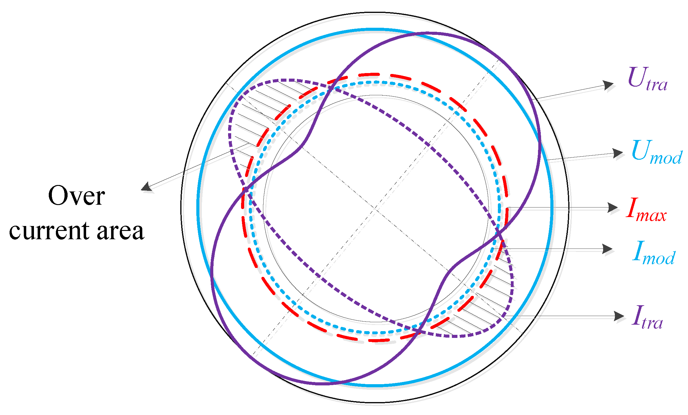
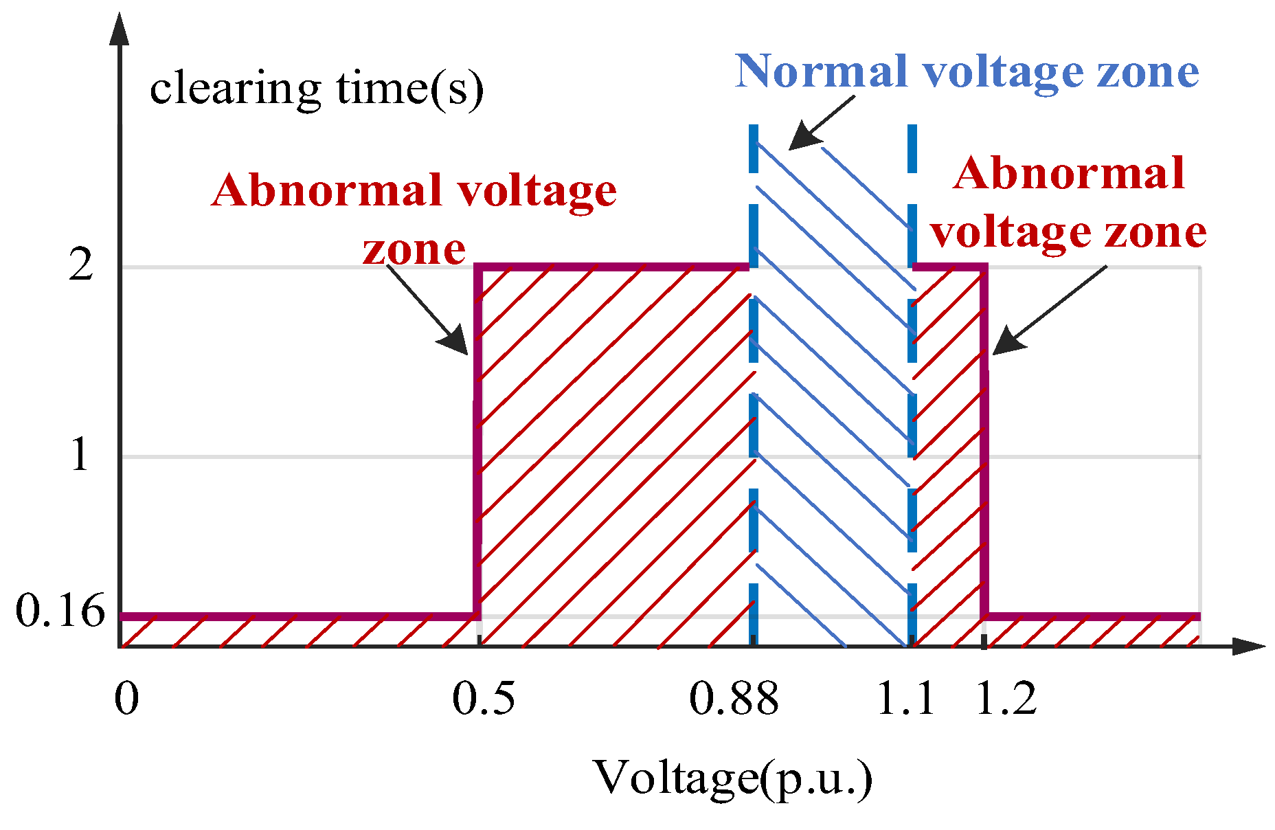
2.2. Deficiency of Traditional Inverter Topology

After Clark transformation, Equation (1) can be written as Equation (13):
[ u α u β ] = 2 3 [ 1 1 2 1 2 0 3 2 3 2 ] [ u a u b u c ] = [ u α + + u α u β + + u β ]
where
[ u α + u β + ] = [ U + sin ( ω t + θ v p ) U + cos ( ω t + θ v p ) ] [ u α u β ] = [ U sin ( ω t + θ v n ) U cos ( ω t + θ v n ) ]
Three-phase output currents can be written as Equation (14):
[ i α i β ] = 2 3 [ 1 1 2 1 2 0 3 2 3 2 ] [ i a i b i c ] = [ i α + + i α i β + + i β ]
where
[ i α + i β + ] = [ I + sin ( ω t + θ i p ) I + cos ( ω t + θ i p ) ] [ i α i β ] = [ I sin ( ω t + θ i n ) I cos ( ω t + θ i n ) ]
The instantaneous output power is given as Equation (15):
[ p q ] = [ v α i α + v β i β v α i β v β i α ] = [ P 0 + P c 2 cos ( 2 ω t ) + P s 2 sin ( 2 ω t ) Q 0 + Q c 2 cos ( 2 ω t ) + Q s 2 sin ( 2 ω t ) ]
where P0 is the DC component value of active power, Pc2 and Ps2 are the coefficients of cosine and sinusoidal terms for the second oscillation value of active power, Q0 is the DC component value of reactive power, Qc2 and Qs2 are the coefficients of cosine and sinusoidal terms for the second oscillation value of reactive power.
P0, Pc2, Ps2, Q0, Qc2 and Qs2 can be expressed by matrix as Equation (16):
[ P 0 Q 0 P c 2 P s 2 Q c 2 Q s 2 ] = [ v d + v q + v d v q v q + v d + v q v d v d v q v d + v q + v q v d v q + v d + v q v d v q + v d + v d v q v d + v q + ] [ i d + i q + i d i q ]
where v d + , v q + are the dq axis components of u α + , u β + ; v d , v q are the dq axis components of u α , u β ; i d + , i q + are the dq axis components of i α + , i β + ; i d , i q are the dq axis components of i α , i β after Park transformation, respectively.
When the output current meets the grid codes [18,19], the negative-sequence current should be set as zero, then Equation (16) will be changed into Equation (17):
[ P 0 Q 0 P c 2 P s 2 Q c 2 Q s 2 ] = [ v d + v q + v q + v d + v d v q v q v d v q v d v d v q ] [ i d + i q + ] .
In Equation (16), the rank of the coefficient matrix is 4, the rank of the augmented matrix is 5. The rank of the coefficient matrix is not equal to the rank of the augmented matrix, so Equation (16) has no solution. This is the reason why the control strategy in [10,11,12,13,14] has difficulty eliminating the power oscillation.
In Equation (17), the rank of the coefficient matrix is 2, the rank of the augmented matrix is 3. The rank of the coefficient matrix is not equal to the rank of the augmented matrix, so Equation (17) has no solution. This is the reason why the BPSC control strategy has difficulty eliminating power oscillation for the traditional topology.
In the same way, it can be found that after adding a zero-sequence component in [15], Equation (17) becomes:
[ P 0 Q 0 P c 2 P s 2 Q c 2 Q s 2 ] = [ v d + v q + v Re 0 v Im 0 v q + v d + 0 0 v d v q v Re 0 v Im 0 v q v d v Im 0 v Re 0 v q v d 0 0 v d v q 0 0 ] [ i d + i q + i Re 0 i Im 0 ]
where v Re 0 , v Im 0 are the real and imaginary components of zero-sequence voltage at PCC, i Re 0 , i Im 0 are the real and imaginary components of zero-sequence output current, the detailed definition refers to [15].
In (18), the rank of the coefficient matrix is 4, the rank of the augmented matrix is 5. The rank of the coefficient matrix is not equal to the rank of the augmented matrix, so Equation (18) has no solution. This is the reason why the BPSC control strategy has difficulty eliminating power oscillation for three-phase four-wire inverter in [15].

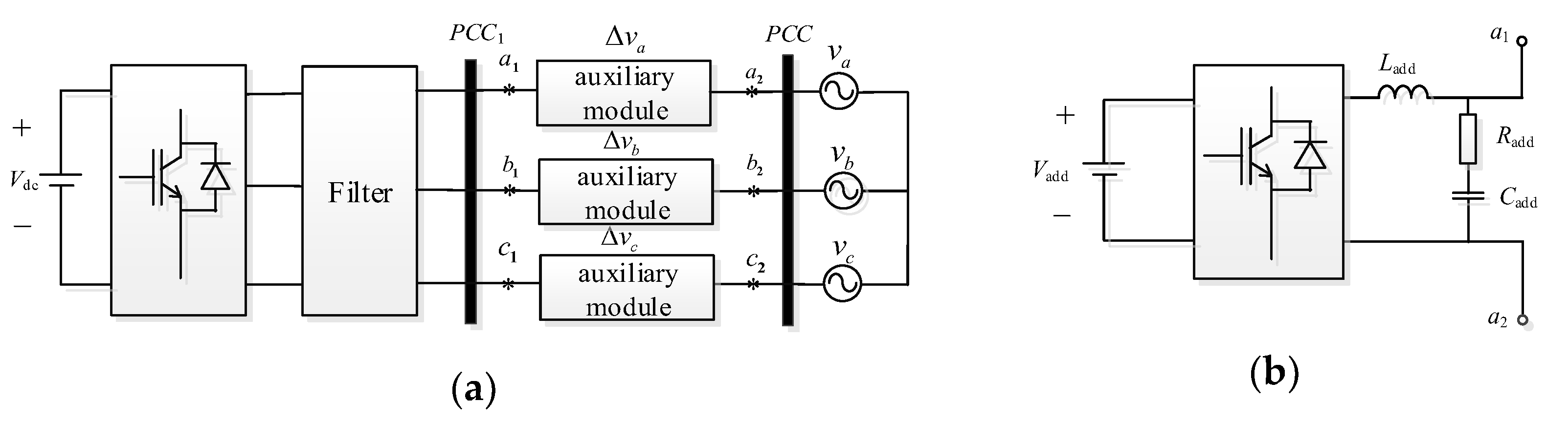
3. Principle and Advantages of Modified Topology for Grid-Connected Inverter

According to the discussion in Section 2, the reason why the traditional topology is incapable of eliminating the power oscillation is that the number of controllable free variables is small, which leads to the mismatch between the order of the current reference coefficient matrix and the order of the augmented matrix. From the point of view on hardware, the number of controllable variables in the current reference equation can be increased by changing the topology structure, so that the equation can meet the solvability conditions.

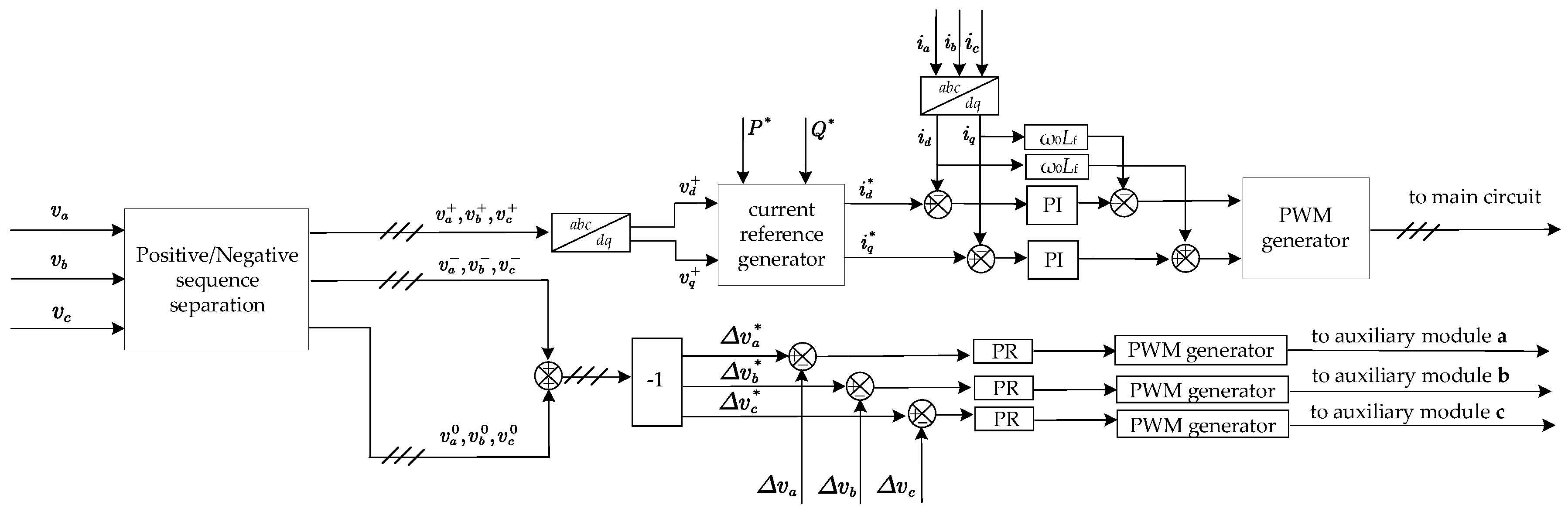
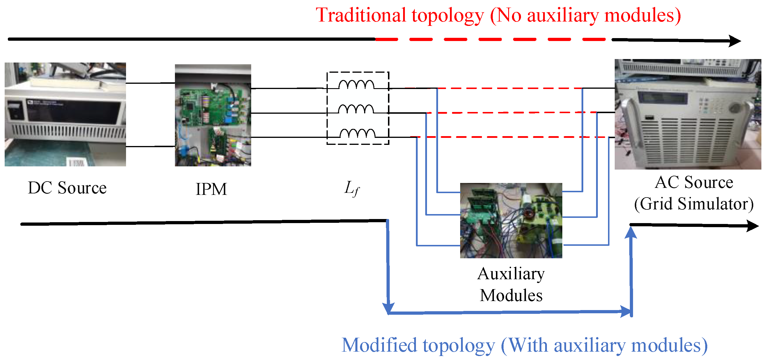
3.1. Modified Topology of Grid-Connected Inverters

The proposed topology of grid-connected inverter is shown in Figure 3. The auxiliary modules are inserted in series between the output filter of inverter (the points a1, b1 and c1 in Figure 3a) and PCC (the points a2, b2 and c2 in Figure 3a).
The three-phase auxiliary modules are independent of each other and can be separately controlled. Figure 3b shows the detailed internal block diagram of the auxiliary module which is essentially a single-phase inverter. Ladd and Cadd constitute the output filter circuit of the auxiliary module to filter the switching subharmonics in the circuit. Radd is the damping resistance of the output filter circuit to prevent the possible oscillation of the LC filter circuit. For the voltages at PCC1, Equation (19) could be obtained as:
v a 1 = v a + Δ v a v b 1 = v b + Δ v b v c 1 = v c + Δ v c  
where Δ v a , Δ v b and Δ v c are the output voltages of auxiliary modules in phases A, B and C, respectively.
Accordingly, Equation (17) can be changed into Equation (20):
[ P 0 Q 0 P c 2 P s 2 Q c 2 Q s 2 ] = [ v d + + Δ v d + v q + + Δ v q + v q + + Δ v q + v d + Δ v d + v d Δ v d v q Δ v q v q Δ v q v d + Δ v d v q Δ v q v d + Δ v d v d + Δ v d v q + Δ v q ] [ i d + i q + ]
where Δ v d + , Δ v q + are the positive-sequence dq axis components of Δ v a , Δ v b and Δ v c ; Δ v d , Δ v q are the negative sequence dq axis components of Δ v a , Δ v b and Δ v c after positive and negative-sequence separation and Park transformation.
When the output of the auxiliary module is set to satisfy Equation (21):
Δ v d = v d Δ v q = v q Δ v d + = 0 Δ v q + = 0 ,
a new equation, Equation (22) can be obtained from Equation (20):
[ P 0 Q 0 P c 2 P s 2 Q c 2 Q s 2 ] = [ v d + v q + v q + v d + 0 0 0 0 0 0 0 0 ] [ i d + i q + ] .
It can be further simplified as Equation (23):
[ v d + v q + v q + v d + ] [ i d + i q + ] = [ P * Q * ] .
The coefficient matrix rank of Equation (23) is 2, the rank of the augmented matrix is 2. The number of equations is equal to the number of variables, so that Equation (23) has a unique solution. The corresponding current reference value can be solved as Equation (24):
[ i d * i q * ] = [ i d + i q + ] = [ v d + v q + v q + v d + ] 1 [ P * Q * ] .
When it is needed to limit the current, the upper limit of the reference current can be adjusted by changing the value of Δ v d + and Δ v q + in Equation (21).
The overall control structure of the system is shown in Figure 4. After positive and negative sequence separation module, positive-sequence components v a + , v b + and v c + , negative-sequence components v a , v b and v c , and zero-sequence components v a 0 , v b 0 and v c 0 are derived from PCC voltages v a , v b and v c . Following that, v d + and v q + are generated from v a + , v b + , v c + through abc/dq transformation. Then, the current reference values i d * and i q * are given from current reference generator module according to Equation (24). After that, the current reference values i d * and i q * generate the PWM waves that control the main circuit through the PI module as well as processing the decoupling components ω 0 L f i d and ω 0 L f i q . The negative-sequence voltage components v a , v b , v c and the zero-sequence voltage components v a 0 , v b 0 , v c 0 are added and then create reference values Δ v a * , Δ v b * , Δ v c * of the auxiliary module output voltage by multiplying by minus one. The three reference values Δ v a * , Δ v b * and Δ v c * , respectively, generate PWM waves for three auxiliary module circuits through the PR controller.
The Decoupled Double Synchronous Reference Frame Phase-Locked Loop (DDSRF-PLL), which has better performance under unbalanced voltage, is adopted to achieve phase detection [21]. The structure of DDSRF-PLL is shown in Figure 5. After positive and negative sequence abc/dq transformation, v d + , v q + , v d and v q are derived from the grid voltage va, vb and vc. Then, v d + * , v q + * are generated from v d + , v q + after a decoupling network. Similar to the phase detection principle of the Synchronous Reference Frame Phase-Locked Loop (SRF-PLL) [21], the phase of the system θ ^ could be obtained by making v q + * approach zero through the PI controller. The detailed structure of decoupling network is expressed as in [21].

3.2. Advantages of Modified Topology

The voltage and current vector trajectories of the traditional topology and the modified topology are shown in Figure 6 [9], respectively. When single-phase voltage fault occurs, the trajectory of voltage vector will be distorted. When the voltage vector trajectory shows a spindle-shaped variation, as the trajectory of Utra in Figure 6, in order to keep the output power constant, the trajectory of the current amplitude becomes an ellipse, as the trajectory of Itra in Figure 6. Where, Imax is the maximum value of the allowable current amplitude of the system. It can be seen that the amplitude of Itra has exceeded the value of Imax near the long axis of the actual current track, as shown in the shaded area, which may give rise to over-current fault. When the auxiliary modules are inserted into the system, the unbalanced voltage is corrected to a standard circle, as the trajectory of Umod in Figure 6, and the corresponding current amplitude trajectory is also a standard circle, as the trajectory of Imod in Figure 6. Since the amplitude of Umod can be adjusted by changing the value of Δ v d + and Δ v q + , so that the radius of the trajectory of Umod can be ensured not to be too small, then the corresponding trajectory of Imod can be guaranteed to be included in the circular trajectory of Imax, so as to avoid the risk of overcurrent fault.

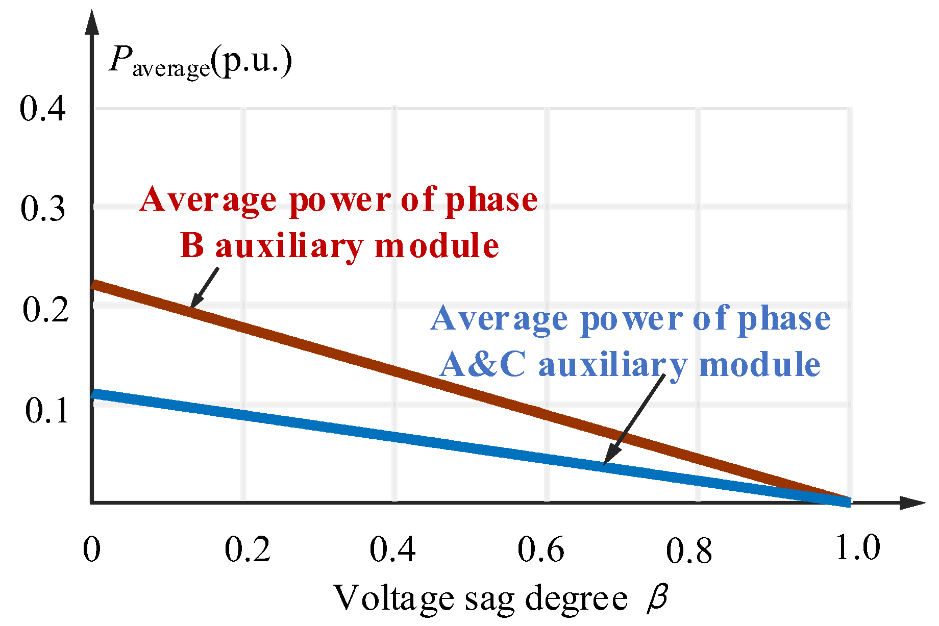
3.3. Capacity Design of Auxiliary Modules

Supposing that the fault occurs in phase B, and the voltage amplitude of phase B is β times of its original normal value, then the vector format of three-phase voltage is described as Equation (25):
V a = V φ V b = β V ( φ 120 ° ) V c = V ( φ + 120 ° )  
The positive, negative and zero-sequence voltage components of phase A are obtained as Equation (26), [21].
[ V a ( 1 ) V a ( 2 ) V a ( 0 ) ] = 1 3 [ 1 h h 2 1 h 2 h 1 1 1 ] [ V a V b V c ] = [ 2 + β 3 V φ 1 β 3 V ( φ 60 ° ) 1 β 3 V ( φ + 60 ° ) ]
where
h = e j 120 ° = 1 2 + j 3 2 h 2 = e j 240 ° = 1 2 j 3 2
The positive, negative and zero-sequence voltage components of phase B and phase C are obtained as Equations (27) and (28):
[ V b ( 1 ) V b ( 2 ) V b ( 0 ) ] = [ 2 + β 3 V ( φ 120 ° ) 1 β 3 V ( φ + 60 ° ) 1 β 3 V ( φ + 60 ° ) ]
[ V c ( 1 ) V c ( 2 ) V c ( 0 ) ] = [ 2 + β 3 V ( φ + 120 ° ) 1 β 3 V ( φ + 180 ° ) 1 β 3 V ( φ + 60 ° ) ] .
In the modified topology, the average powers of the three auxiliary modules are shown in Equation (29):
P a = 1 β 6 V I P b = 1 β 3 V I P c = 1 β 6 V I .
When β changes between [0, 1], the power curve of the auxiliary module is shown in Figure 7. Auxiliary module of the fault phase-phase B essentially injects power into the circuit. When the output power of the grid-connected inverter is used as the power base value, which is P b a s e = ( 3 / 2 ) V I , the maximum value of the injected power is 0.22 p.u. (β = 0). Phases A and C are non-fault phases. Their auxiliary modules absorb power from the circuit, and the maximum absorbed power is 0.11 p.u. (β = 0). Therefore, for the single-phase voltage fault, the power capacity of the auxiliary module designed above 0.22 p.u. can meet the requirements no matter what the drop depth is and no matter which phase the fault occurs in.
According to the clearing time of inverters under voltage faults shown in Figure 8, in case of voltage drop, the grid-connected inverter only needs to maintain the connection time of 2 s at most. Therefore, the energy needed to be absorbed or released by the auxiliary module will not be too large, and the operation of the inverter during the LVRT period will not cause damage to the energy storage devices in the auxiliary module.

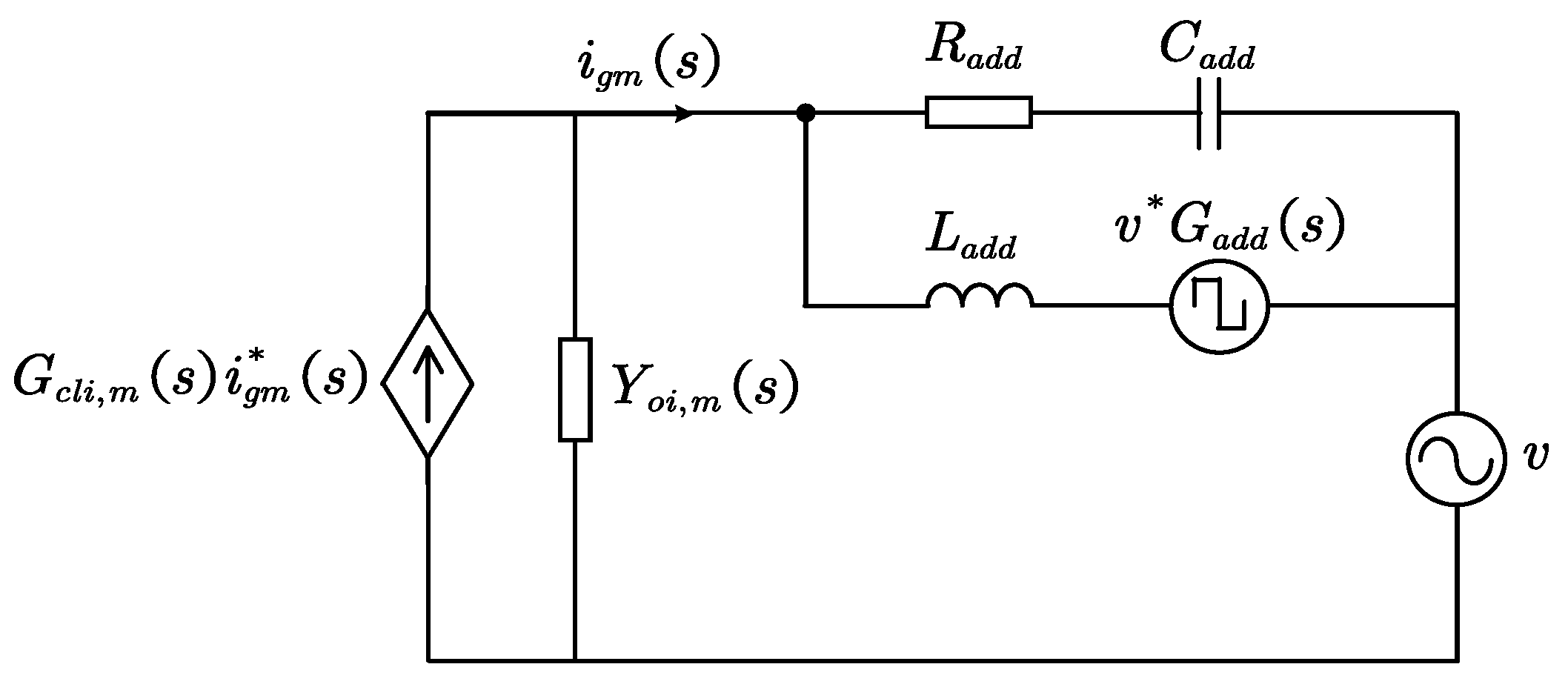
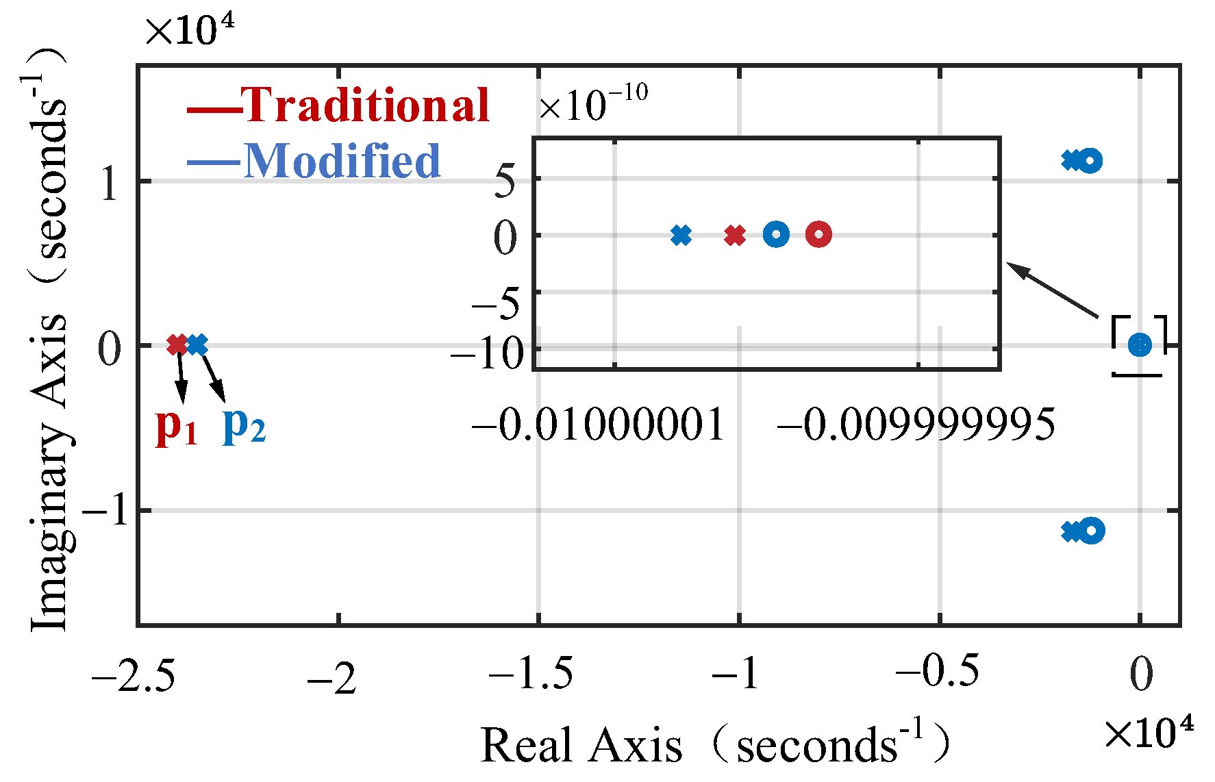
3.4. Stability Analysis of the Modified Topology

Since the parameters of the three branches of the inverter are identical, according to [7,22], the whole system can be simplified shown in Figure 9.
In Figure 9, v * is the output voltage reference of the auxiliary module, G a d d ( s ) is the transfer function of the auxiliary module voltage in open mode. L a d d , C a d d and R a d d are inductance, capacitor and resistor of the auxiliary module, respectively. G c l i , m ( s ) denotes the current reference to output transfer function of grid-connected inverter, Y o i , m ( s ) represents the equivalent output admittance of the system, i g m * ( s ) and i g m ( s ) are the reference current and output current of system, respectively, and their detailed form are expressed as [22].
When we adopt the parameters in Table 3, Table 4 and Table 5, the pole-zero maps of the current closed transfer functions for the traditional topology and the modified topology are shown in Figure 10, respectively. In Figure 10, p1 and p2 are the dominant closed-loop poles of the current transfer function for the traditional topology and the modified topology, respectively. Although p2 is closer to the imaginary axis than p1, they are still very close to each other and far away from the imaginary axis. Therefore, compared with the traditional topology, the output stability of the modified topology is reduced, but all poles of the modified topology system are still in the left half plane and the whole system is still stable.

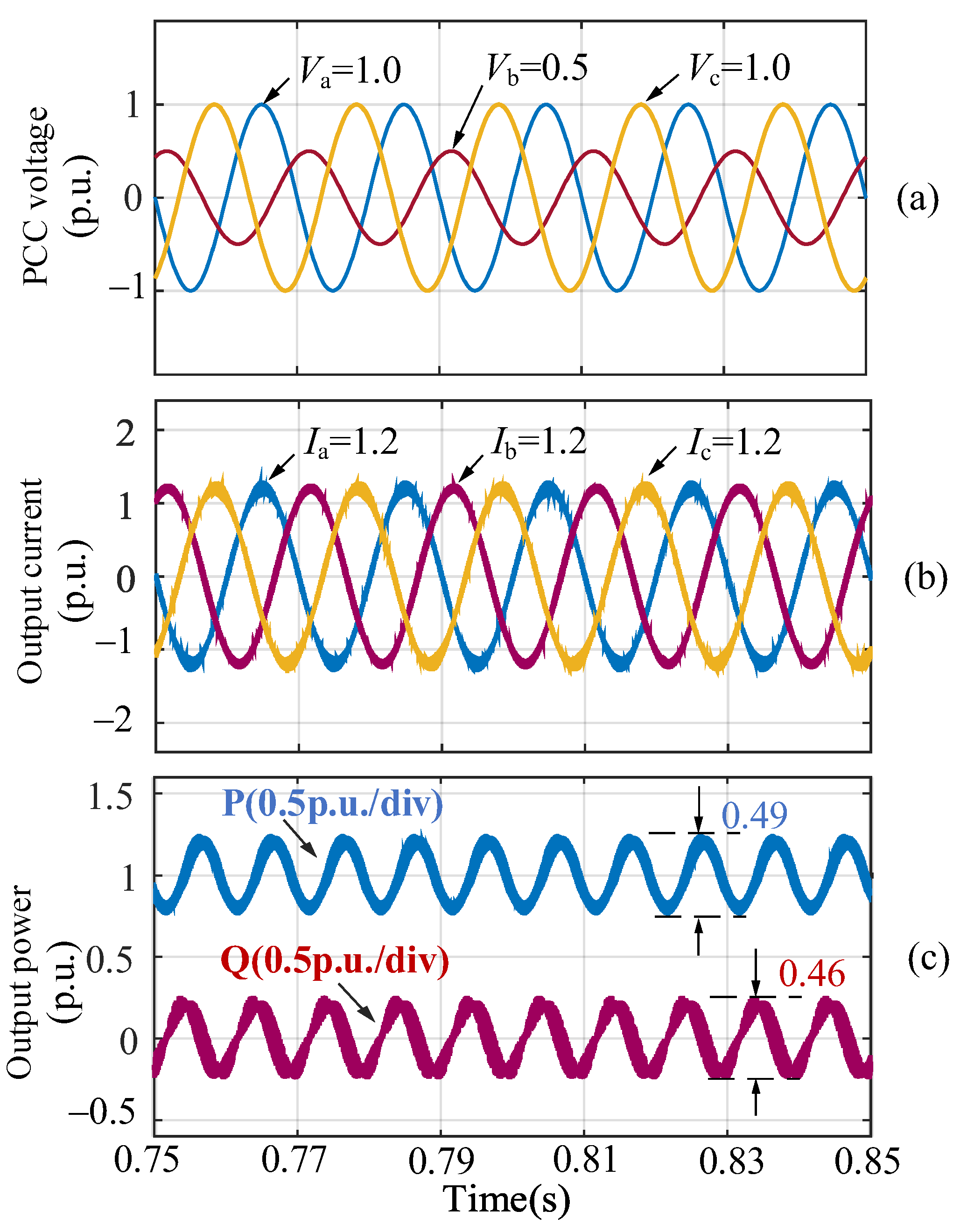
4. Simulation Results

With the detailed discussion of the modified topology, the MATLAB/Simulink was performed to achieve the verification. In the simulation, the fault type is that the voltage of phase B drops to 0.5 p.u. The parameters of other main circuits are shown in Table 2, and the parameters of the auxiliary modules are shown in Table 5. The results of the traditional topology and the modified topology are shown in Figure 11 and Figure 12, respectively.
Comparing the results in Figure 11 and Figure 12, when the modified topology is adopted, the unbalanced voltage at PCC1 can be corrected, and the inverter output current keeps being balanced. The oscillation value of the output active power is reduced from 0.49 to 0.17 p.u., and the output reactive power oscillation value is reduced from 0.46 to 0.15 p.u. The oscillation value of active power for the modified topology is 33.88% of that of the traditional topology and the reactive power oscillation value is reduced to 32.17% of the value of traditional topology. The simulation results show that the modified topology can correct the unbalanced voltage at the output of the inverter and reduce the oscillation of the output active power and reactive power.

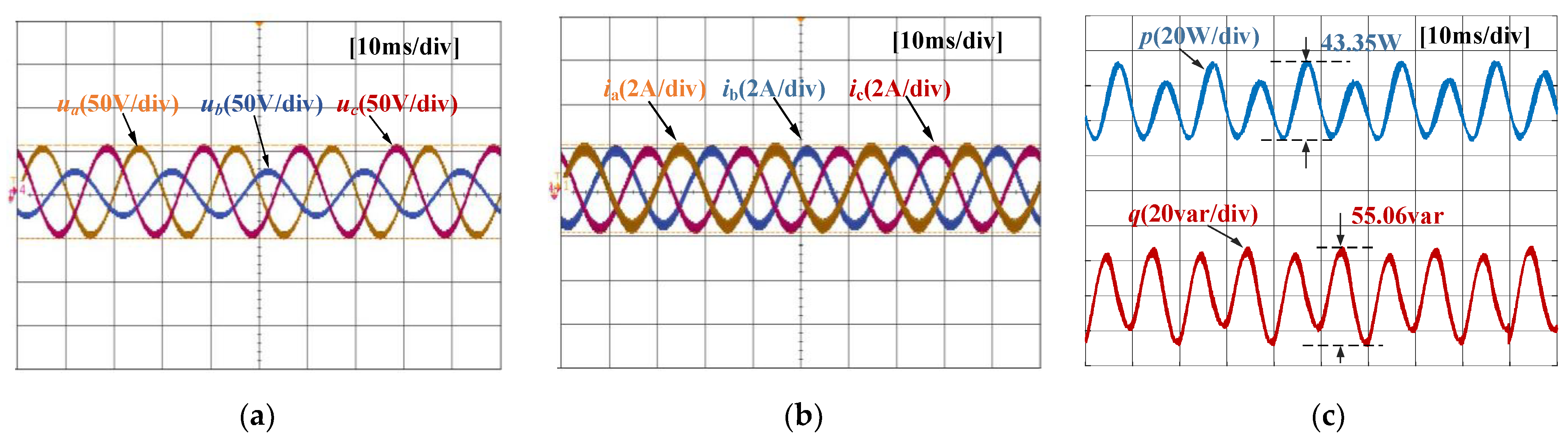
5. Experimental Results

In order to confirm the simulation results, the three-phase converter was verified by downscaling the levels of voltage and power. The overall configuration of the experimental setup is shown in Figure 13. The core control algorithm is implemented on TMS320F28335, while the intelligent power module (IPM) is PM150RLA120. IT6516C DC source is used to generate DC voltage and Chroma 61702 AC source is implemented to generate AC voltage to simulate grid voltage. The auxiliary module consists of three identical single-phase inverters, all of which adopt the filter composed of Ladd, Radd and Cadd. Lf is the filter inductance of grid-connected inverter output circuit. In the experiment, the fault type is that the voltage of phase B drops to 0.5 p.u. The parameters of other main circuits are shown in Table 3, and the parameters of auxiliary modules are shown in Table 4. The experimental results of the traditional topology and the modified topology are shown in Figure 14 and Figure 15, respectively.
Comparing the results of the traditional topology and the modified topology in Figure 14 and Figure 15, the unbalanced voltage at PCC1 can be corrected under the modified topology, and the inverter output current keeps balanced. The oscillation value of the output active power is reduced from 43.35 to 13 W, and the output reactive power oscillation value is reduced from 55.06 to 15.08 var. The oscillation value of active power in the modified topology is 29.99% of that in traditional topology and the reactive power oscillation value is reduced to 27.39% of the value of the traditional topology. The experimental results show that the modified topology can correct the unbalanced voltage at the output of the inverter and reduce the oscillation of the output active power and reactive power.

6. Conclusions

The grid-connected inverter with modified topology could compensate the negative-sequence and the zero-sequence components of the output voltage, so that the reference current equation of the inverter meets the solvability condition, thus eliminating the output power oscillation while the output current waveform still meets the requirements of grid codes. The simulation and experimental results show that the modified topology can effectively correct the unbalanced voltage and reduce the output active power oscillation and reactive power oscillation.
When the grid voltage is balanced, grid voltage does not contain negative-sequence components and zero-sequence components. Therefore, the output voltage reference value of the auxiliary module is zero at this time, and the auxiliary module will not output voltage, nor will it absorb power from the circuit or inject power to circuit. The auxiliary module is always connected to the circuit regardless of the unbalanced grid voltage fault or normal grid voltage, but when the grid voltage is balanced, the auxiliary module will not play a role.
The auxiliary voltage source can be a DC voltage source, a large capacitor, a super capacitor, or other energy storage units. This article aims to illustrate the function of the auxiliary module, so in the experiment, only the DC voltage source is used. In the future, the methods of using large capacitors or other energy storage structures to replace the additional DC power source in the auxiliary module and also designing the effective charging and discharging topologies of auxiliary modules as well as reducing the cost of hardware will be explored.

Author Contributions

Conceptualization, C.L., X.M. and L.Y.; methodology, C.L., X.M. and L.Y.; software, C.L. and Y.L.; validation, C.L., X.Y. and J.R.; data curation, Y.Z.; writing—original draft preparation, C.L. and X.M.; supervision, X.M.; project administration, X.M. All authors have read and agreed to the published version of the manuscript.

Funding

This work was supported by China Scholarship Council under Grant 202006280458.

Institutional Review Board Statement

Not applicable.

Informed Consent Statement

Not applicable.

Data Availability Statement

Not applicable.

Conflicts of Interest

The authors declare no conflict of interest.

References

  1. Blaabjerg, F.; Liserre, M.; Ma, K. Power electronics converters for wind turbine systems. IEEE Trans. Ind. Appl. 2012, 48, 708–719. [Google Scholar] [CrossRef] [Green Version]
  2. Jia, J.; Yang, G.; Nielsen, A.H. Investigation of grid-connected voltage source converter performance under unbalanced faults. In Proceedings of the 2016 IEEE PES Asia-Pacific Power and Energy Engineering Conference (APPEEC), Xi’an, China, 25–28 October 2016; pp. 609–613. [Google Scholar]
  3. Tleis, N. Power Systems Modeling and Fault Analysis: Theory and Practice, 1st ed.; Elservier: Amsterdam, The Netherlands, 2008. [Google Scholar]
  4. Nian, H.; Cheng, P.; Zhu, Z.Q. Independent operation of DFIG-based WECS using resonant feedback compensators under unbalanced grid voltage conditions. IEEE Trans. Power Electron. 2015, 30, 3650–3661. [Google Scholar] [CrossRef]
  5. Taul, M.G.; Wang, X.; Davari, P.; Blaabjerg, F. An overview of assessment methods for synchronization stability of grid-connected converters under severe symmetrical grid faults. IEEE Trans. Power Electron. 2019, 34, 9655–9670. [Google Scholar] [CrossRef] [Green Version]
  6. Taul, M.G.; Wang, X.; Davari, P.; Blaabjerg, F. Current reference generation based on next generation grid code requirements of grid-tied converters during asymmetrical faults. IEEE J. Emerging Sel. Top. Power Electron. 2020, 8, 3784–3797. [Google Scholar] [CrossRef] [Green Version]
  7. Wang, X.; Blaabjerg, F.; Chen, Z.; Wu, W. Resonance analysis in parallel voltage-controlled distributed generation inverters. In Proceedings of the 2013 Twenty-Eighth Annual IEEE Applied Power Electronics Conference and Exposition (APEC), Long Beach, CA, USA, 17–21 March 2013; pp. 2977–2983. [Google Scholar]
  8. Rocabert, J.; Luna, A.; Blaabjerg, F.; Rodríguez, P. Control of power converters in AC microgrids. IEEE Trans. Power Electron. 2012, 27, 4734–4749. [Google Scholar] [CrossRef]
  9. Ng, C.H.; Ran, L.; Bumby, J. Unbalanced-grid-fault ride-through control for a wind turbine inverter. IEEE Trans. Ind. Appl. 2008, 44, 845–885. [Google Scholar] [CrossRef]
  10. Rodriguez, P.; Timbus, A.V.; Teodorescu, R.; Liserre, M.; Blaabjerg, F. Flexible active power control of distributed power generation systems during grid faults. IEEE Trans. Ind. Electron. 2007, 54, 2583–2592. [Google Scholar] [CrossRef]
  11. Guo, X.; Liu, W.; Zhang, X.; Sun, X.; Lu, Z.; Guerrero, J. Flexible control strategy for grid-connected inverter under unbalanced grid faults without PLL. IEEE Trans Power Electron. 2015, 30, 1773–1778. [Google Scholar] [CrossRef] [Green Version]
  12. Guo, X.; Liu, W.; Lu, Z. Flexible power regulation and current-limited control of grid-connected inverter under unbalanced grid voltage faults. IEEE Trans. Ind. Electron. 2017, 64, 7425–7432. [Google Scholar] [CrossRef]
  13. Camacho, A.; Castilla, M.; Miret, J.; Borrell, A.; de Vicuña, L.G. Active and reactive power strategies with peak current limitation for distributed generation inverters during unbalanced grid faults. IEEE Trans. Ind. Electron. 2015, 62, 1515–1525. [Google Scholar] [CrossRef] [Green Version]
  14. Du, X.; Wu, Y.; Gu, S.; Tai, H.; Sun, P.; Ji, Y. Power oscillation analysis and control of three-phase grid-connected voltage source converters under unbalanced grid faults. IET Power Electron. 2016, 9, 2162–2173. [Google Scholar] [CrossRef]
  15. Ma, K.; Chen, W.; Liserre, M.; Blaabjerg, F. Power controllability of a three-phase converter with an unbalanced AC source. IEEE Trans. Power Electron. 2015, 30, 1591–1604. [Google Scholar] [CrossRef]
  16. Saccomando, G.; Svensson, J.; Sannino, A. Improving voltage disturbance rejection for variable-speed wind turbines. IEEE Trans. Energy Conv. 2002, 17, 422–428. [Google Scholar] [CrossRef]
  17. Jia, J.; Yang, G.; Nielsen, A.H. A review on grid-connected converter control for short-circuit power provision under grid unbalanced faults. IEEE Trans. Power Deliv. 2018, 33, 649–661. [Google Scholar] [CrossRef] [Green Version]
  18. IEEE Standard 929. IEEE Recommended Practice for Utility Interface of Photovoltaic (PV) Systems; IEEE: Piscataway, NJ, USA, 2000. [Google Scholar]
  19. IEEE Standard 1547. IEEE Standard for Interconnecting Distributed Resources with Electric Power Systems; IEEE: Piscataway, NJ, USA, 2003. [Google Scholar]
  20. Mortazavian, S.; Shabestary, M.M.; Mohamed, Y.A.I. Analysis and dynamic performance improvement of grid-connected voltage-source converters under unbalanced network conditions. IEEE Trans. Power Electron. 2017, 32, 8134–8149. [Google Scholar] [CrossRef]
  21. Teodorescu, R.; Liserre, M.; Rodriguez, P. Grid Converters for Photovoltaic and Wind Power Systems, 1st ed.; Wiley: Hoboken, NJ, USA, 2011. [Google Scholar]
  22. Wang, X.; Blaabjerg, F.; Wu, W. Modeling and analysis of harmonic stability in an AC power-electronics-based power system. IEEE Trans. Power Electron. 2014, 29, 6421–6432. [Google Scholar] [CrossRef]
Figure 1. Maximum value of output current amplitude varying with the adjustment coefficient.
Energies 14 05057 g001
Figure 2. Oscillation value of output power varying with the adjustment coefficient.
Energies 14 05057 g002
Figure 3. Structure block diagram of the modified topology of grid-connected inverter: (a) general system diagram. (b) Auxiliary module block diagram.
Energies 14 05057 g003
Figure 4. Overall control structure diagram.
Energies 14 05057 g004
Figure 5. The structure of DDSRF-PLL.
Energies 14 05057 g005
Figure 6. Change of voltage and current amplitude trajectories of the traditional and the modified topologies.
Energies 14 05057 g006
Figure 7. Output power of the auxiliary module.
Energies 14 05057 g007
Figure 8. Clearing time of inverters under different voltage faults.
Energies 14 05057 g008
Figure 9. Equivalent structure diagram of the modified topology.
Energies 14 05057 g009
Figure 10. Pole-zero maps of current closed transfer functions for the traditional topology and the modified topology.
Energies 14 05057 g010
Figure 11. Simulation results of the traditional topology, when Vb drops to 0.5 p.u. (a) Output voltage at PCC1; (b) output current; (c) output active power and reactive power.
Energies 14 05057 g011
Figure 12. Simulation results of the modified topology, when Vb drops to 0.5 p.u. (a) Output voltage at PCC1; (b) output current; (c) output active power and reactive power.
Energies 14 05057 g012
Figure 13. Configuration of the experimental setup.
Energies 14 05057 g013
Figure 14. Experimental results of the traditional topology, when Vb drops to 0.5 p.u. (a) Output voltage at PCC1; (b) output current; (c) output active power and reactive power.
Energies 14 05057 g014
Figure 15. Experimental results of the modified topology, when Vb drops to 0.5 p.u. (a) Output voltage at PCC1; (b) output current; (c) output active power and reactive power.
Energies 14 05057 g015
Table 1. Output effect under different adjustment coefficient k.
kControl StrategyCharacteristics
Oscillation CancellationCurrent Quality
Active PowerReactive Power
1Average Active Reactive Control××
0Balanced Positive Sequence Control××
−1Positive Negative Sequence Control××
Other valueTrade-off between power oscillation cancellation and current quality
Table 2. Operating parameters of main circuit used in simulations.
SymbolDescriptionValue (p.u.)
VaAmplitude value of A-phase voltage220 2   V (1 p.u.)
VbAmplitude value of B-phase voltage110 2   V (0.5 p.u.)
VcAmplitude value of C-phase voltage220 2   V (1 p.u.)
P0Output power10 kW (1 p.u.)
f0Fundamental frequency50 Hz
fswOperating frequency10 kHz
LfOutput inductor0.044 p.u.
VdcDC voltage700 V
kpProportional coefficient2.0
kiIntegral coefficient1.0
Table 3. Operating parameters of main circuit used in experiments.
SymbolParameterValue (p.u.)
VaAmplitude value of A-phase voltage 50 V (1 p.u.)
VbAmplitude value of B-phase voltage 25 V (0.5 p.u.)
VcAmplitude value of C-phase voltage50 V (1 p.u.)
P0Output power105 W (1 p.u.)
f0Fundamental frequency50 Hz
fswOperating frequency10 kHz
LfOutput inductor0.044 p.u.
VdcDC voltage120 V
kp
ki
Proportional coefficient
Integral coefficient
2.0
2.0
Table 4. Operating parameters of auxiliary module used in experiments.
SymbolParameterValue
VaddDC voltage of auxiliary module 36 V
fadd Switching frequency of auxiliary module10 kHz
CaddFilter capacitor of auxiliary module 15 μF
LaddFilter inductor of auxiliary module 800 μH
RaddDamping resistance of auxiliary module 2.0 Ω
kp
kr
Proportional coefficient
Resonant coefficient
0.01
4.0
Table 5. Parameters of auxiliary module used in simulations.
SymbolParameterValue
VaddDC voltage of auxiliary module150 V
faddSwitching frequency of auxiliary module10 kHz
CaddFilter capacitor of auxiliary module15 μF
LaddFilter inductor of auxiliary module800 μH
RaddDamping resistance of auxiliary module2.0 Ω
kp
kr
Proportional coefficient
Resonant coefficient
0.02
16.91
Publisher’s Note: MDPI stays neutral with regard to jurisdictional claims in published maps and institutional affiliations.

