Article

Technical Limits of Passivity-Based Control Gains for a Single-Phase Voltage Source Inverter

by
Zbigniew Rymarski
and
Krzysztof Bernacki
*
Department of Electronics, Electrical Engineering and Microelectronics, Faculty of Automatic Control, Electronics and Computer Science, Silesian University of Technology, Akademicka 16, 44-100 Gliwice, Poland
*
Author to whom correspondence should be addressed.
Energies 2021, 14(15), 4560; https://doi.org/10.3390/en14154560
Submission received: 16 June 2021 / Revised: 16 July 2021 / Accepted: 22 July 2021 / Published: 28 July 2021

Abstract

:
Passivity-based control (PBC) seems to be predicted for the control algorithms in the voltage source inverters (VSI) for voltage backup systems. This paper presents limitations of the improved (IPBC) version of the PBC (directly measuring the output voltage) maximum voltage and current gains. In a microprocessor-controlled inverter, these depend on the PWM modulator dynamic properties, the switching frequency, the modulation index value (avoiding modulator saturation and enabling the rapid increase of the filter inductor current), and the parameters of the VSI output filter. A single switching period delay of the digital PWM modulator was considered in the theoretical calculations based on a discrete inverter model. The simulations for the standard nonlinear rectifier RC load enabled the initial adjustment of the IPBC border gains, which depended on the switching frequency. Some small harmonics oscillations of the output voltage were acceptable for the test rectifier RC load or dynamic load. However, oscillations of the inductor current increased the power losses in the coil core. Experimental verification of the simulation results using a laboratory VSI model is also presented.

Graphical Abstract

1. Introduction

Passivity-based controls (PBC) were introduced into control algorithms more than 20 years ago. PCB is a method reminiscent of standard Lyapunov methods [1]. At first, it was used in electromechanical systems as an Interconnection and Damping Assignment Passivity-Based Control (IDA-PBC) [1,2]. More recently, different PBC versions are among the most promising control systems for voltage source inverters that work on-grid [3,4] or off-grid in AC voltage backup systems, single-phase voltage source inverters [5,6,7,8,9], or three-phase inverters [10,11,12].
AC voltage backup systems, e.g., uninterruptible power supplies (UPS), have requirements associated with the distortions of the output voltage for precisely defined loads [13,14,15,16]. All investigations should consider two basic standard loads—nonlinear rectifier RC with PF = 0.7 (PF is a product of the displacement factor and the distortion factor [17]) and the dynamic load. The component non-linear load values have been precisely defined elsewhere [13]. A VSI should reduce the value of the Total Harmonic Distortion (THD) coefficient of the output voltage (for Low Voltage < 1 kV, THD < 8%, harmonic amplitude maximum < 5%). This was a typical load for a UPS with an output power of less than 3 kW and is the subject of our research.
The undershoot, overshoot and settling time for a dynamic load change were 20–100% and 100–20% as defined in [13] for other VSI output voltage parameters. For a load step increase during the first switching period, the feedback loop does not work due to the delay of the PWM modulator—the output capacitor should contain a stored charge, and the step increase of the voltage would be forced on the output filter inductance. Step voltages that increase at the output sinusoidal voltage maximum point only have amplitudes of (1–M)*VDC, where M is the modulation index and VDC is the input DC voltage of the inverter. We should force a rapid increase of the current through the filter coil (lower inductance values mean better control). In the case of a step load decrease (the worst case is at the voltage maximum), the output overvoltage depends on the capacity of the output capacitor and the instantaneous inductor current. The filter inductor works as the current source (the feedback has a one switching period delay) that forces the charge flow to the output filter capacitor for the switched-off load, which results in a voltage overshoot. The feedback works during the next switching period. The quality of the output voltage decreases for overly large filter inductances values, a capacitance that is too low (a large capacitance results in the reactive power in the output filter components, which causes excess power losses on the equivalent serial resistances of the inverter), and an excessive modulation index, which eliminates the possibility of a rapid increase of the filter inductor current.
In our opinion, the main problem with the PBC design stems from setting up the gain values (the “injected resistance” Ri for the inductor current control and the gain Kv of the output voltage error in the improved PBC-IPBC versions) when considering the technical possibilities of a digitally controlled inverter. Higher gains correspond to higher rates of theoretical error convergence; however, a real system with a control loop begins to oscillate. A basic theoretical analysis of the root locus of the characteristic polynomial of a closed-loop system showed that a positive sum of the injected resistance Ri and the equivalent serial resistance of the inverter and a positive voltage error gain Kv [5,10] was required for the convergence to zero of the tracking errors and maintaining the stability of a system. While the real parts of these poles in a continuous model are theoretically always negative in the s-plane [12], the nonzero imaginary parts in the restricted gain ranges also caused oscillations. Simulations of a VSI with discrete control and experimental verification for a standard nonlinear rectifier RC load proved that increasing IPBC gains from zero initially resulted in a reduction of the output voltage THD coefficient. In the short-range of the IPBC gains, THD was almost the same and additional increases of the Ri and Kv gains increased the THD oscillations of the output voltage [9,12]. Ri and Kv values (their product) always merit consideration. Authors of previous publications tried to determine the upper limitations of the controller gains. A reduction of the injected resistance without considering Kv in [5] was insufficient in our experiments with an IPBC, which was based on the idea of an IDA-PBC control law presented in [10]. Ideas presented in [5] comparing the limited carrier slope in a PWM modulator with the derivative of the control voltage (this derivative should not be faster than the carrier slope in the modulator) were further developed in this paper. We did not consider the carrier slope, but rather the maximum speed of the output PWM modulator voltage increase/decrease (the derivative of the control voltage). A wider discussion of this problem that considered the output voltage error gain Kv was presented in [12]. This paper focuses on the dependence of the maximum allowable gains on the switching frequency of an inverter that was not focused yet. The theoretical analysis, results of MATLAB-Simulink simulations, and experimental VSI model measurements results (controlled with an STM32F407VG microprocessor) were examined at three switching frequencies (12,800 Hz, 25,600 Hz, and 51,800 Hz).
The authors sought to create a control law readily utilized by an engineer-designer of a voltage source off-grid inverter. There are many approaches to the nonlinear modeling of an inverter. The simple linear approach treats the whole inverter plant as an LC filter and one switching period delay in series [9,18,19,20]. The PWM modulation scheme requires dead time implementation between switching on the transistors from the same bridge leg [19,20]. The dead time causes a step decrease of the output voltage when the load current crosses a zero value. This can be treated as nonlinear [21]. However, new switching devices require a short dead time (<500 ns, and was the problem with the “current tail” for older technology IGBTs). The serial resistance and inductance of the filter coils vary and depend on the switching frequency, the coil current, and temperature [22,23,24], which is important for the cheap iron-powder coil core materials. For the alloy powder materials such as Super MSS (Micrometals), this was less important [23,24]. Some approaches for describing the nonlinearity of the coils in the output filter have been reported [25]. We could neglect these nonlinearities for the alloy-powder material, for a constant switching frequency, and the coil current changes around to the operating point.
When creating an inverter model, we usually approximate the PWM modulator as a linear function of the input voltage. We were mindful that when we solved the state equations, the output voltage was an exponential function of the switching on time. We approximated this function with the linear function proposed many years ago [26,27]. Using a double Fourier transform to describe the nonlinear switching function of a converter in the steady-state of an inverter was possible [28]. One approach for analyzing a PWM using the double Fourier transform was initially reported nearly 50 years ago [29,30]. The small-signal models can be compared with the nonlinear model of a switching power electronic converter using the black-box identification method, called the Hammerstein model. In this model, the nonlinear static and linear dynamic characteristics can be considered separately to create an identification model of a power electronic system. The Hammerstein model consists of a static nonlinearity followed by a linear and time-invariable model [31].
The authors used a continuous linearized model [9,18,19,20] with a delay in the PWM modulator in this discussion of the switching frequency influence on the design of an IPBC controller. The discrete control law, which has six coefficients (three of the products of the coefficients and the mutually shifted reference voltages can be presented in the form of the initially calculated look-up tables) is easily implemented in the microprocessor-based controller of a VSI.
Section 2 presents the fundamentals of the PBC controller design and its difference control law. Section 3 contains the calculations that enabled us to determine the border values of the PBC gains above which the oscillations of the output voltage existed due to the technical limits of the inverter and the switching frequency. Section 4 presents the simulations of the VSI operating with the nonlinear rectifier load (according to [13]), the most representative kind of load for the device tests (<3 kW) for the different switching frequencies and different parameters of an inverter filter. Section 5 includes a discussion of the simulation results. Section 6 gives the experimental verification of the simulations from Section 4. Section 7 discusses the experimental verification results and the differences in the values of the border PBC gains in simulations and a real inverter (different scaling of the input variables).

2. Fundamentals of PBC Controller Design

Figure 1 presents the schematic of a multi-input-single-output (MISO) controller in which the load current is treated as an independent disturbance (e.g., [10,32]). While this helps eliminate the load impedance in the control law, feedback from the output voltage to the load current disappears. In some cases, this simplification significantly changes the locus of the characteristic equation poles for a closed-loop system [19]. We used the inductor current and output voltage as the state variables, the load current as a disturbance, and the delay, Ts, as the modulator model.
A PBC is based on the concept that when the supplied energy in a system exceeds the stored energy, the system is passive. The energy in an inverter is stored in two non-dissipative components—the filter coil and the filter capacitor. The energy stored in a system Equation (1) is described by the Hamiltonian function H(x) (in some papers [5], H(x) is called a Lyapunov function).
H ( x ) = 1 2 ( L F i L F 2 + C F v O U T 2 )
That explains why we used the products of Equation (2), LFiLF and CFvOUT, as the state variables (for the other control systems, we used iLF and vOUT as state variables).
x = [ L F i L F C F v O U T ] T
The error vector e is defined Equation (3) where iLFref and vOUTref are the reference values (iLFref is calculated, vOUTref is assigned).
e = [ L F ( i L F i L F r e f ) C F ( v O U T v O U T r e f ) ]
The stored energy of the error values comes from Equation (4).
H ( e ) = 1 2 ( L F ( i L F i L F r e f ) 2 + C F ( v O U T v O U T r e f ) 2 )
The equilibrium of a closed-loop system is asymptotically stable [2] and achieved when H(e) minimizes (5) in x = xref.
H ( e ) x | x = x r e f = 0 ,   2 H ( e ) x 2 | x = x r e f > 0
The system is passive when the energy H(e) of the error decreases with time; therefore, if the time derivative, H(e), is negative in Equation (6),
d H ( e ) d t < 0
Equation (7) describes a closed-loop system [10].
e ˙ = [ J ( R + R a ) ] P 1 e ,   P = [ L F 0 0 C F ] ,   P 1 = [ 1 / L F 0 0 1 / C F ] ,   P 1 e = H ( e ) / e
where the interconnection matrix, J, and the damping matrix, R, are defined as Equation (8).
J = [ 0 1 1 0 ] ,   R = [ R L F 0 0 0 ]
Ra (the PBC controller) is the matrix of the injected damping, Ri is the gain of the current error, and Kv is the conductive gain of the voltage error in Equation (9).
R a = [ R i 0 0 K v ]
Equation (10) describes an open-loop system where m(t − Ts) is a delayed control function (the delay of the PWM modulator) from the previous switching period.
x ˙ = [ J R ] P 1 x + [ V D C 0 ] m ( t T s ) + [ 0 1 ] i O U T
To obtain the control law (11), we subtracted (7) from Equation (10):
[ m ( t T s ) V D C 0 ] = [ L F d i L F r e f / d t C F d v O U T r e f / d t ] + [ ( R L F + R i ) i L F r e f + v O U T r e f i L F r e f + K v v O U T r e f ] [ R i i L F K v v O U T ] + [ 0 1 ] i O U T
Hence, we have the equation of the control law Equation (12) with Equation (13).
v C T R L ( t T s ) = L F d i L F r e f / d t + ( R L F + R i ) i L F r e f + v O U T r e f R i i L F
i L F r e f = C F d v O U T r e f / d t K v ( v O U T v O U T r e f ) + i O U T
A difference control law that considers the Ts delay of the modulator is Equation (14) with Equations (15) and (16)—we have to predict state variables for the k + 1 switching period.
v C T R L ( k ) = L F i L F r e f ( k + 1 ) i L F r e f ( k ) T s + ( R L F + R i ) i L F r e f ( k + 1 ) + v O U T r e f ( k + 1 ) R i i L F ( k + 1 )
i L F r e f ( k ) = C F v O U T r e f ( k ) v O U T r e f ( k 1 ) T s + K v [ v O U T r e f ( k ) v O U T ( k ) ] + i O U T ( k )
i L F r e f ( k + 1 ) = C F v O U T r e f ( k + 1 ) v O U T r e f ( k ) T s + K v [ v O U T r e f ( k + 1 ) v O U T ( k + 1 ) ] + i O U T ( k + 1 )

3. The Influence of the Switching Frequency and Output Filter Parameters on the Border IPBC Gains

Using the inverter state Equations (17) and (18) is the simplest way to predict the vOUT(k + 1), iLF(k + 1) and, finally, to calculate iOUT(k + 1). The presented calculation is based only on a discrete model of an inverter [18,19,20].
v O U T ( k + 1 ) = φ 11 v O U T ( k ) + φ 12 i L F ( k ) + φ 13 i O U T ( k ) + g 11 v C T R L ( k )
i L F ( k + 1 ) = φ 21 v O U T ( k ) + φ 22 i L F ( k ) + φ 23 i O U T ( k ) + g 21 v C T R L ( k )
where the coefficients are presented in Equation (19):
ξ F e = 0.5 R L F e ω F 0 L F e ,   ω F 0 = 1 L F C F , C A = cos ( ω F 0 T s ) exp ( ξ F e ω F 0 T s ) , S A = sin ( ω F 0 T s ) exp ( ξ F e ω F 0 T s ) , ϕ 11 = C A + ξ F e S A ,   ϕ 12 = 1 ω F 0 C F S A , φ 13 = 1 ω F 0 C F S A ( 1 C A ξ F e S A ) R L F e , ϕ 21 = 1 ω F 0 L F e S A ,   ϕ 22 = C A ξ F e S A , ϕ 23 = 1 C A ξ F e S A , φ 31 = 0 ,   φ 32 = 0 ,   φ 33 = 1 ,   C G = cos ( ω F 0 T s / 2 ) exp ( ξ F e ω F 0 T s / 2 ) , S G = sin ( ω F 0 T s / 2 ) exp ( ξ F e ω F 0 T s / 2 ) , g 11 = ω F 0 T s S G , g 21 = 1 L F e T s ( C G ξ F e S G ) ,   g 31 = 0
The output current in the next switching period, iOUT(k + 1), was readily calculated as the difference between the inductor current and the output filter capacitor current in Equations (20) and (21).
i O U T ( k + 1 ) = i L F ( k + 1 ) C F v O U T ( k + 1 ) v O U T ( k ) T s
i O U T ( k + 1 ) = [ φ 21 C F T s ( φ 11 1 ) ] v O U T ( k ) + ( φ 22 C F T s φ 12 ) i L F ( k ) + + ( φ 23 C F T s φ 13 ) i O U T ( k ) + ( g 21 C F T s g 11 ) v C T R L ( k )
The reference inductor current in the next switching period was calculated using the state space Equation (22).
i L F r e f ( k + 1 ) = ( C F T s + K v ) v O U T r e f ( k + 1 ) C F T s v O U T r e f ( k ) + [ φ 21 ( C F T s + K v ) φ 11 + C F T s ] v O U T ( k ) + [ φ 22 ( C F T s + K v ) φ 12 ] i L F ( k ) + + [ φ 23 ( C F T s + K v ) φ 13 ] i O U T ( k ) + [ g 21 ( C F T s + K v ) g 11 ] v C T R L ( k )
The predicted increase of the reference inductor current in the next switching period is described with Equation (23).
i L F r e f ( k + 1 ) i L F r e f ( k ) = ( C F T s + K v ) v O U T r e f ( k + 1 ) ( 2 C F T s + K v ) v O U T r e f ( k ) + C F T s v O U T r e f ( k 1 ) + [ φ 21 ( C F T s + K v ) φ 11 + C F T s + K v ] v O U T ( k ) + [ φ 22 ( C F T s + K v ) φ 12 ] i L F ( k ) + [ φ 23 ( C F T s + K v ) φ 13 1 ] i O U T ( k ) + [ g 21 ( C F T s + K v ) g 11 ] v C T R L ( k )
The difference control law of the IPBC of a single-phase inverter, which considers the delay of the PWM discrete modulator is expressed by Equation (24).
v C T R L ( k ) = A V R E F 1 v O U T r e f ( k + 1 ) + A V R E F 2 v O U T r e f ( k ) + A V R E F 3 v O U T r e f ( k 1 ) + + A V O U T 4 v O U T ( k ) + A I L F 5 i L F ( k ) + A I O U T 6 i O U T ( k )
where Equation (25):
R e = L F T s + R L F + R i ,   K e = C F T s + K v A V R E F 1 = ( R e K e + 1 ) 1 + R e K e g 11 ( L F T s + R L F ) g 21 , A V R E F 2 = C F T s R e L F T s K e 1 + R e K e g 11 ( L F T s + R L F ) g 21 , A V R E F 3 = 1 ω F 0 2 T s 2 1 + R e K e g 11 ( L F T s + R L F ) g 21 , A V O U T 4 = R e K e φ 11 + ( L F T s + R L F ) φ 21 + C F T s R e + L F T s K e 1 ω F 0 2 T s 2 1 + R e K e g 11 ( L F T s + R L F ) g 21 A I L F 5 R e K e φ 12 + ( L F T s + R L F ) φ 22 1 + R e K e g 11 ( L F T s + R L F ) g 21 , A I O U T 6 = R e K e φ 13 + ( L F T s + R L F ) φ 23 L F T s 1 + R e K e g 11 ( L F T s + R L F ) g 21
However, we can use the reference voltage shifted by one switching period and the final discrete control law used is Equation (26).
v C T R L ( k ) = A V R E F 1 v O U T r e f ( k ) + A V R E F 2 v O U T r e f ( k 1 ) + A V R E F 3 v O U T r e f ( k 2 ) +   + A V O U T 4 v O U T ( k ) + A I L F 5 i L F ( k ) + A I O U T 6 i O U T ( k )
The calculated values of the variables in the next switching period might be inaccurate because we use the discretized model of the inverter directly [18,19,20]. More exact results were obtained when we would estimate the state variables at the next sampling instant using the full order state observer [33,34]. We would use the same state equations but would sum them with the gain matrix of the estimator multiplied by the difference between the measured and estimated system output variable (the output voltage). However, the complexity of the calculations is difficult to use in practice, though additional simulations showed that the simplified approach was satisfactory.
The basic frequency of the closed-loop system oscillations was caused by the higher speed (derivative) of the control voltage increase than the speed (derivative) of the PWM modulator control voltage change. The restrictions of the PBC gains depend on the maximum speed (derivative) of the PWM modulator control voltage increase. The maximum increase speed of the vCTRL voltage in Equation (27) cannot be faster than the maximum increase speed of the PWM modulator control voltage.
v C T R L ( k ) v C T R L ( k 1 ) T s ( A V R E F 1 + A V R E F 2 + A V R E F 3 ) Δ v O U T r e f T s + + A V O U T 4 ( v O U T ( k ) v O U T ( k 1 ) T s ) + A I L F 5 ( i L F ( k ) i L F ( k 1 ) T s ) + A I O U T 6 ( i O U T ( k ) i O U T ( k 1 ) T s )
The maximum increase speed of the sinusoidal reference voltage, vOUTref is expressed using Equations (28) and (29), where M is a modulation index.
d ( M V D C sin ( 2 π 50 t ) ) d t | max = M V D C 2 π 50
v O U T r e f ( k + 1 ) v O U T r e f ( k ) T s | max v O U T r e f ( k ) v O U T r e f ( k 1 ) T s | max v O U T r e f ( k 1 ) v O U T r e f ( k 2 ) T s | max Δ v O U T r e f T s | max = M V D C 2 π 50  
The maximum speed of the output voltage increase will occur for a step load decrease to zero for the maximum control voltage when the filter inductor operates like the voltage source iLF and loads the charge to the output capacitor CF. For this calculation, we approximated the inductor current as constant during one switching period in this case Equation (30). We did not consider a short circuit of the inverter output.
v O U T ( k ) v O U T ( k 1 ) T s | max = Δ v O U T T s | max i L F ( k ) C F | max , V D C L F T s < i L F ( k ) < V D C L F T s , V D C L F C F T s < Δ v O U T T s | max , min < V D C L F C F T s
The maximum speed of the increase/decrease of the inductor current occurred for the zero crossing of the output voltage Equation (31).
i L F ( k ) i L F ( k 1 ) T s = Δ i L F T s , V D C L F < Δ i L F T s | max , min < V D C L F
The maximum increase/decrease of the output current caused by the control action can be equal to the difference/sum of the inductor current increase and the output capacitor current increase/decrease (Equation (32)). We did not consider a short circuit of the inverter output when the changes of the output voltage and the current were much higher and depended on the parasitic resistance of the capacitor. The value obtained from Equation (33) is only indicative.
i O U T ( k ) i O U T ( k 1 ) T s = Δ i O U T T s = Δ i L F Δ v O U T C F / T s T s = Δ i L F T s Δ v O U T T s 2 C F
0 < Δ i O U T T s | max , min < 2 V D C L F
It should be noted the assumed maximum values of the increases of the voltages and currents only appeared in specific cases of the dynamic load change, e.g., when the current to the load was cut off by the rectifier diode for a rectifier RC load. This is the standard [13] load for UPS systems up to 3 kW. We calculated the maximum value of (ΔvCTRL/Ts)max using Equations (27)–(33). The speed (derivative) of the voltage increase in a three-level PWM modulator is expressed by Equation (34).
d ( t T s V D C ) d t = V D C T s ,   where   0 < t < T s
The final indicative inequality that should be maintained to avoid oscillations is shown in Equation (35).
d v C T R L d t < V D C T s ,   v C T R L ( k ) v C T R L ( k 1 ) T s < V D C T s
The simulations shown in Figure 2a–c (for LF = 1 mH, CF = 50 μF, RLF = 1 Ω, and M = 0.5) for three switching frequencies (12,800, 25,600 and 51,200 Hz) help estimate the border values (below the control voltage oscillations) of the voltage gain Kv (Figure 2d) as a function of the current gain Ri. RLF equals the serial equivalent resistance of the inverter when power losses in the inverter are considered [22,23,24].
The border values of the IPBC gains depended on the parameters of the output filter. Figure 3a–d show the border gain dependence as a function of the filter inductance, LF = 0.5–2 mH, for CF = 50 μF, RLF = 1 Ω, M = 0.5, and fs = 25,600 Hz.
Figure 4 illustrates how the border gains depend on filter capacitances CF = 10–100 μF for LF = 1 mH, RLF = 1 Ω, M = 0.5, and fs = 25,600 Hz.
The dependence of the maximum IPBC gains on the switching frequency, the output filter inductor, and the output filter capacitor are presented in Figure 2, Figure 3 and Figure 4. Higher inductor and capacitor values correspond to higher PBC border gains. The assumed values of the possible changes of the inductor current, output current, and output voltage were only indicative.

4. Simulations of a VSI with an IPBC for a Nonlinear Rectifier RC Load

The simulations in MATLAB 2020b should determine initially identified areas of IPBC gains without control voltage oscillations (Figure 5a,b and Figure 6a). The standard nonlinear rectifier RC load (PF = 0.7) was selected based on the results reported in [13]. However, gains over the border values, which caused some oscillations of the control voltage (Figure 6b), resulted in lower distortions of the output voltage (lower THD).
In simulations and the experimental inverter, the first scheme of a three-level double edge PWM modulation was used [19,20,22] in which the frequency of the bridge transistor switches is a double 2fs switching (control) frequency fs. Some small additional power losses [35] occurred when we allowed small oscillations of the inductor current. The power losses in the magnetic material of the filter coil core (neglecting so-called excess power losses) are shown presented as (36) where k1 is the coefficient of the hysteresis losses and k2 is the coefficient of the eddy current losses and the flux density is a linear function of the magnetizing current. We used a Super-MSS (Sendust) alloy-powder (soft magnetic material) core [36,37] (MS 184075-2) for which the hysteresis power losses were much lower than the eddy current losses (k1 << k2fn).
P l o s s e s = n = 1 n = I L F h n max 2 ( k 1 f n + k 2 f n 2 ) = n = 1 n = I L F h n max 2 ( k 1 + k 2 f n ) f n n = 1 n = k 2 I L F h n max 2 f n 2
Increasing the IPBC gains yielded the minimum THDVOUT of the output voltage by allowing some oscillations of the inductor current, and we decreased the power efficiency (Table 1).
Δ P l o s s e s [ % ] = 100 P o s c P b o r d e r P b o r d e r [ % ] 100 ( n = 1 n = I L F h n max o s c 2 f n 2 n = 1 n = I L F h n b o r d e r 2 f n 2 1 ) [ % ]
Δ P l o s s e s [ % ] 100 ( I L F h 1 max o s c 2 n = 1 n = I L F h n max o s c 2 I L F h 1 max o s c 2 n 2 I L F h 1 max b o r d e r 2 n = 1 n = I L F h n max b o r d e r 2 I L F h 1 max b o r d e r 2 n 2 1 ) %
However, when the border gain values were Ri = 20 and Kv = 1.41 and for gains, Ri = 30 and Kv = 30 that resulted in oscillations for fs = 51,200 Hz, the theoretical relative increase of the power losses in the magnetic material was negligible (in the experimental inverter, the increase in the power losses was much higher).

5. Discussion of the Simulation Results

An analysis of the simulation results showed the following:
  • For the frequencies analyzed (12,800, 25,600, and 51,200 Hz), it was important to consider the delay of the PWM modulator in the control law. Even the simplest prediction of the variables in the next switching period using the discrete state space equations allowed an estimation of the PBC border gains to lower distortions of the inverter output voltage and a better dynamic load change response.
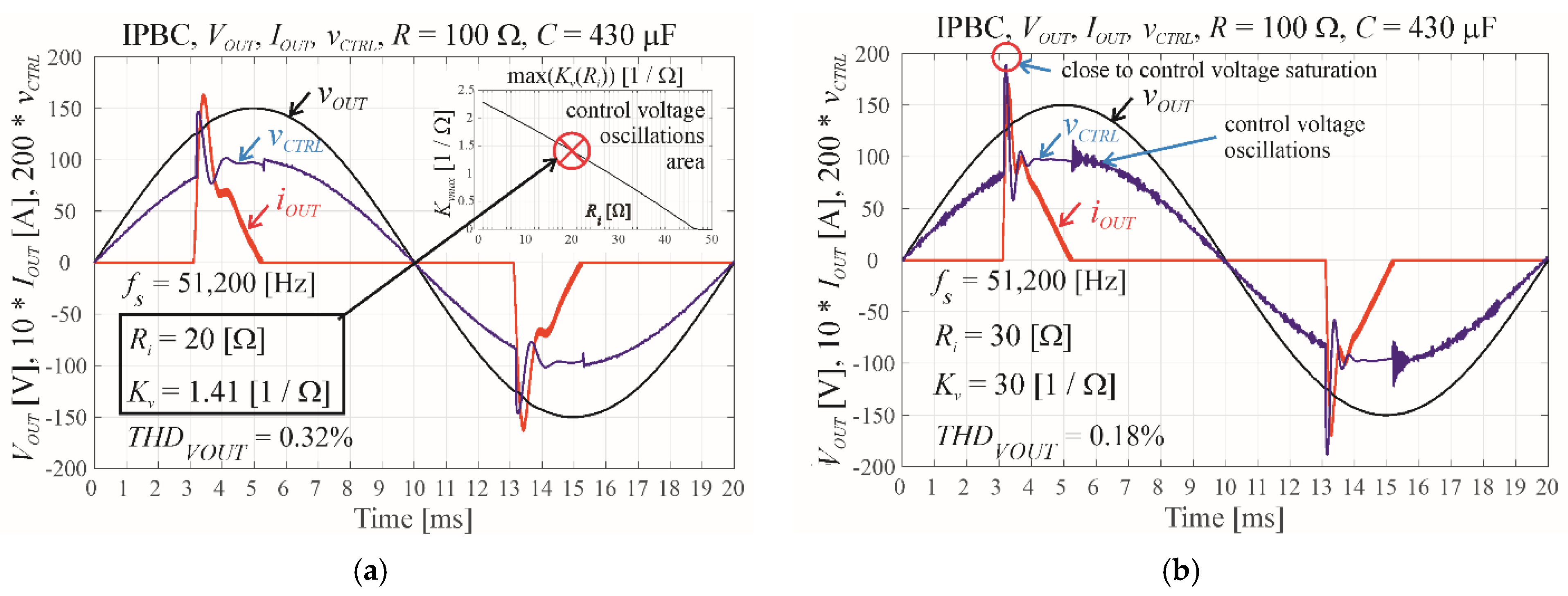
  • Basic PBC theory does not enable the limits of the PBC gains to be found. For positive gains, a system is always theoretically stable [9]. The technical properties of an inverter control system cause the restrictions. Below the border gains of the PBC, there are no output voltage oscillations. The border gains are calculated based on the assumption that the increase of the control voltage should not be faster than the possible increase of the PWM modulator voltage (VDC voltage in one switching period Ts).
  • Additional gain increases over the border values causes oscillations of the output voltage and the inductor current and output voltage distortions. It is possible to find the maximum gains of the PBC for the minimum of the output voltage THD.
  • A lower modulation index, M, is preferable—it is a (1–M)VDC margin of voltage that forces an inductor current increase. However, low values of M will not be used in a practical design because we always allow for the potential of full input voltage (M close to unity).
  • A lower M helps avoid saturation of the PWM modulator (Figure 6b) for higher controller gains.
  • The oscillations of the inductor current slightly increase the power losses in the inductor core.
  • The results shown in Table 1 confirm the preference for using a higher switching frequency. However, we should not forget about potential technical problems. In one switching period, we count up to a value that equals the PWM comparator frequency divided by the switching frequency. In the experimental work, we used an STM32F407VG microprocessor with an 84 MHz frequency in the PWM modulator. Using fs = 51,200 Hz (1024 switching time periods per fundamental period), we obtained the maximum counted value per switching period of ≈1640 (the amplitude of the sinusoidal reference waveform was 820). The resolution, 1/820 = 1.2 × 10⁻³, was insufficient for the generated sinusoidal waveform close to π because the change of 1 − sin(2π × (256 − 1)/1024) = 1.8825 × 10⁻⁵, was lower than the resolution. It caused the width of some (in our case 16) neighboring PWM pulses of the reference waveform close to π/2 or 3π/2 to be the same; however, in this case, the additional distortions were ignored (ΔTHD = 0.051%). Therefore, fs = 51,200 Hz was assigned as the highest switching frequency for the STM32F407VG microprocessor control.

6. Experimental Verification

The experimental inverter parameters (Figure 7): three-level, double edge, the first modulation scheme PWM [19,20,22], fs = 51,200 Hz, CF = 50 μF, LF = 1 mH, RLF = 1 Ω, M = 0.5, RC load: R = 50 Ω, C = 430 μF, dynamic load (500||50)/500 Ω). RLF is a series equivalent resistance of the inverter and was measured [24] for a filter coil with the core: Super-MSS™–Sendust (MS), MS-184075-2, μ = 75, AL = 169, and le = 0.10743 m [36]. A STM32F407VG (32 bit, 168 MHz) microprocessor controlled the inverter. The border gains, Ri and Kv, were selected experimentally and therefore were not directly compared to the theoretical gains because they were multiplied by the output voltage and current scaling factors.
Figure 8 shows the Bode plots of the plant (the inverter with PWM modulator). The Bode plots were measured for the relative amplitude values of the sinusoidal waveforms and phases for frequencies ranging from 100 Hz to 5000 Hz relative to the fundamental frequency (50 Hz) waveform in the input of the PWM modulator and the fundamental frequency waveform of the output voltage of the inverter. A relative measurement was required because the modulator input uses modulator units (the maximum amplitude equaled 820 units for fs = 51,200 Hz, 1640 for fs = 25,600 Hz, and 3280 for fs = 12,800 Hz), and the output voltage uses volts. This dimensionless measurement is precisely described in [22,23,24]. Figure 8 also shows that the switching frequency for the coil with the Super-MSS core did not significantly influence the Bode plots of the inverter.
The other components of the experimental model were the measurement traces (including an Analog-to-Digital Conversion—ADC) of the output voltage, output current, and coil current. All traces were similar except for the sensors that ensured galvanic isolation (isolated amplifier ISO 124P in the output voltage trace and LA-25NP current transducers in the output current and the inductor current traces). Both sensors had a much higher bandwidth than the plant and the rest of the measurement trace (ISO 124P has a small-signal bandwidth of 50 kHz and a slew rate of 2 V/μs, and LA-25 NP has a bandwidth of 150 kHz). Therefore, the dynamic characteristics (the magnitude and the phase) of the output voltage measurement trace should represent all three traces up to 5000 Hz. Figure 9a,b give the Bode plots of the output voltage measurement trace (including the galvanic isolation and ADC).
The relative magnitude of the traces was approximately 0 dB (from −0.25 dB to 0.4 dB for fs = 25,600 Hz, and 51,200 Hz), and the phase-shifted. We can approximate the magnitude and the phase plots with the simple delay 2Ts (two switching periods). It seemed that output voltage damping 40 dB/decade over the resonant frequency (712 Hz) sufficiently maintained the phase margin of the loop. There were no additional low pass filters (except for the antialiasing filters). However, for gains over the border values, the oscillations could have come from a phase delay of the entire loop; a higher switching frequency corresponds to a smaller loop delay and higher frequency oscillations. The amplification of the voltage trace was adjusted so that for the output nominal amplitude of the output voltage fundamental harmonic for the 50 Ω load, we could read 3000 units of the ADC (it ranged from −4095–+4095). This was treated as the voltage scale ratio equal to unity. For the 50 Ω load resistance, which was assumed as nominal, we adjusted the amplification of this current trace to get 2000 units from the ADC reading. Therefore, the output current scaling ratio was (3000/2000)/50 = 0.03. For the small output capacitor (1 μF), the same adjustment procedure was performed for the inductor current trace to obtain the same current scaling ratio of 0.03. It was important to adjust the voltage and current scaling factors carefully because they were multiplied by the PBC controller gains. In the simulations, the voltage and current scaling factors were simply 1/VDC for the maximum amplitude of the reference waveform equal to 1. For the experimental inverter, the reference amplitudes were 3280, 1640, and 820 for the 12,800 Hz, 25,600 Hz, and 51,200 Hz switching frequencies, respectively. In all cases, we used 3000 units for the voltage and 2000 units for currents as nominal ADC values. Therefore, to compare the simulation and the experiment, the experimentally assigned gains were multiplied by r(12,800 Hz) = 3000/3280 = 0.915, r(25,600 Hz) = 3000/1640 = 1.829, and r(51,200 Hz) = 3000/820 = 3.659 for 12,800, 25,600, and 51,200 Hz. The recalculated gains were assigned as Ri’ = r*Ri and Kv’ = r*Kv. Figure 10, Figure 11, Figure 12, Figure 13 and Figure 14 present the results of the PBC control for the border gains and the values above them.

7. Discussion of the Experimental Results

The recalculated (Ri’, Kv’) experimental border gains differed from those previously appointed theoretically: Ri = 5, Kv = 0.23 vs. Ri’ = 1.83, Kv’ = 0.183 for 12,800 Hz, Ri = 10, Kv = 0.69 vs. Ri’ = 5.49, Kv’ = 0.92 for 25,600 Hz and Ri = 20, Kv = 1.41 vs. Ri’ = 10.98, Kv’ = 1.83 for 51,200 Hz. Figure 15 presents the recalculated values of the border gains Ri’, Kv’, which closely approximated the theoretically appointed border gain curves. Higher switching frequencies led to better compatibility of theory and measurements.
The theoretical results were perfect. The experimental inverter had voltage and current measurement traces from which the Bode plots (Figure 9a,b) approximated as a delay of about 2Ts [24]. Higher switching frequencies led to better agreement between simulation and experimental results (Table 2). Lower measurement trace delays (2Ts; Figure 9) resulted in higher possible gains and lower output voltage distortions. However, the 40 dB/decade damping of the plant (inverter) above 700 Hz (in the presented experimental model) should maintain a safe phase margin. The linearization of the inverter model at higher switching frequencies resulted in a lower error because there was a more precise linear approximation of the exponential function (used in the discrete model [19,20]) for shorter switching periods. Measurement trace delays led to lower gain oscillation values (above the border values) than in simulations. At higher switching frequencies, the oscillation frequencies increased (the measuring trace delays decreased with switching frequency)—900 Hz for fs = 12,800 Hz, 1150 Hz for fs = 25,600 Hz, and 1350 Hz for fs = 51,200 Hz. The power loss increases in the core of the coil between two sets of gains Ri = 3, Kv = 0.5, Ri’ = 10.98, Kv’ = 1.83 (close to the border values) and Ri = 3, Kv = 0.7, Ri’ = 10.98, Kv’ = 1.83 above the border values was 18.6%.
The IPBC controller design should begin by calculating the border curve from simulations for the particular parameters of the inverter and the chosen switching frequency (Figure 2d, Figure 3d and Figure 4d). Then we should appoint the recalculated gains Ri’, Kv’ on or below the border curve. We physically adjust the output voltage amplifiers to obtain the assigned value (in units) ADCV of the ADC for the amplitude of the nominal voltage. After such an operation, we assign a unity gain in the voltage amplification trace (in our example ADCV = 3000 for the nominal output voltage amplitude). We adjusted the output current amplifiers to obtain the assigned value (in units) ADCI of the ADC (in our example ADCI = 2000) for the amplitude of the output current for the nominal resistive RNOM load. For the lowest possible output capacitor, we proceeded the same way for the inductor current. The scaling ratios of voltage and currents were sv = 1, sI = (ADCV/ADCI)/RNOM (in our example sI = 0.03). These scaling factors were implemented in the inverter control software. For the PWM comparator input frequency fPWM (in our example, fPWM = 84 MHz) and the switching frequency fs (in our example, 12,800, 25,600, and 51,200 Hz), we determined the maximum amplitude of the reference waveform fPWM/fs (in our example, it was 3280, 1640, or 820). That meant we should use the recalculation factor r = ADCV/(fPWM/fs) (for us, it was r(12800 Hz) = 0.915, r(25600 Hz) = 1.829, and r(51200 Hz) = 3.658 for fs = 12800, 25,600 and 51,200 Hz). If we chose the recalculated PBC gains Ri’, Kv’ from the border curve, we can calculate the PBC gains that we have to use in the inverter software Ri = Ri’/r, Kv = Kv’/r.

8. Conclusions

The paper presents the basic reasons for restricting PBC controller gains. Previously reported basic theoretical considerations showed that positive PBC gains have no limitations and the poles of the characteristic equation of the closed-loop system were always in the left half of the s-plane. However, the first limitation is the control signal speed increase above the possible speed of the increase in a PWM double edge, three-level modulator. The second limitation was modulator signal saturation. This limitation could be relaxed for the tolerably lower inductance of the output filter coil or the lower modulation index [12]. The third limitation came from delays in the measurement traces (depending on the design) and in the same PWM modulator (it is always one switching period). The delay of the PWM modulator was considered in the control law using the state space equations to predict the state variables of a discrete, linearized inverter model. A more sophisticated solution involves using a Luenberger state observer; however, the final equations were extremely complex, and theoretical results showed that the use of simple state space equations sufficed. Higher switching frequencies resulted in higher PBC controller gains and lower output voltage distortions. The simulations and the experimental model had different scaling coefficients of the voltage and currents. That explains why the border gains of the controller in the simulations and the directly adjusted gains (Ri, Kv) in the experimental model were different. However, after recalculation of the adjusted experimental model border gains with the scaling factors that differed significantly from simulation results, the recalculated gains (Ri’, Kv’) closely approximated the theoretical border curves (Figure 15). The most general conclusion drawn in the paper stems from the possibility of using higher PBC gains for higher switching frequencies, and better reduces output voltage distortions for standard linear and nonlinear loads.

Author Contributions

Conceptualization, Z.R. and K.B.; methodology, Z.R. and K.B.; software, Z.R.; validation, Z.R. and K.B.; formal analysis, Z.R. and K.B.; investigation, Z.R. and K.B.; resources, Z.R. and K.B.; writing—original draft preparation, Z.R.; writing—review and editing, Z.R. and K.B.; visualization, Z.R.; supervision, Z.R.; project administration, Z.R. and K.B.; funding acquisition, Z.R. and K.B. All authors have read and agreed to the published version of the manuscript.

Funding

The authors were supported by a pro-quality grant of the Rector of the Silesian University of Technology, Zbigniew Rymarski, grant number: 02/140/RGJ21/0013 and Krzysztof Bernacki 02/140/RGJ21/0011. This research was partially supported by the Polish Ministry of Education and Science funding for statutory activities (BK/RAU11/2021).

Institutional Review Board Statement

Not applicable.

Informed Consent Statement

Not applicable.

Conflicts of Interest

The authors declare no conflict of interest.

References

  1. Ortega, R.; Garcıa-Canseco, E. Interconnection and Damping Assignment Passivity-Based Control: A Survey. Eur. J. Control 2004, 10, 432–450. [Google Scholar] [CrossRef]
  2. Wang, Z.; Goldsmith, P. Modified energy-balancing-based control for the tracking problem. IET Control Theory Appl. 2008, 2, 310–312. [Google Scholar] [CrossRef]
  3. Cupertino, A.F.; Carlette, L.P.; Perez, F.; Resende, J.T.; Seleme, S.I., Jr.; Pereira, H.A. Use of Control Based on Passivity to Mitigate the Harmonic Distortion Level of Inverters. In Proceedings of the 2013 IEEE PES Conference on Innovative Smart Grid Technologies (ISGT Latin America), Sao Paulo, Brazil, 15–17 April 2013; pp. 1–7. [Google Scholar] [CrossRef]
  4. Biel, J.M.; Scherpen, A. Passivity-based control of active and reactive power in single-phase PV inverters. In Proceedings of the 2017 IEEE 26th International Symposium on Industrial Electronics (ISIE), Edinburgh, UK, 19–21 June 2017; pp. 999–1004. [Google Scholar] [CrossRef]
  5. Komurcugil, H. Improved passivity-based control method and its robustness analysis for single-phase uninterruptible power supply inverters. IET Power Electron. 2015, 8, 1558–1570. [Google Scholar] [CrossRef]
  6. Rymarski, Z.; Bernacki, K.; Dyga, Ł. Some aspects of voltage source inverter control. Elektron. Ir Elektrotechnika 2017, 23, 26–30. [Google Scholar] [CrossRef] [Green Version]
  7. Zhang, Z.; Yao, N.; Wang, C.; Kang, L.; Kang, L. A Passivity-based Control Method for the Single-Phase Three-level Inverter. In Proceedings of the 18th International Conference on Electrical Machines and Systems (ICEMS), Pattaya City, Thailand, 25–28 October 2015; pp. 1515–1518. [Google Scholar]
  8. Rymarski, Z.; Bernacki, K.; Dyga, Ł. Decreasing the single-phase inverter output voltage distortions caused by impedance networks. IEEE Trans. Ind. Appl. 2019, 55, 7586–7594. [Google Scholar] [CrossRef]
  9. Rymarski, Z.; Bernacki, K. Different Features of Control Systems for Single-Phase Voltage Source Inverters. Energies 2020, 13, 4100. [Google Scholar] [CrossRef]
  10. Serra, F.M.; De Angelo, C.H.; Forchetti, D.G. IDA-PBC control of a DC–AC converter for sinusoidal three-phase voltage generation. Int. J. Electron. 2016, 104, 93–110. [Google Scholar] [CrossRef]
  11. Rymarski, Z.; Bernacki, K.; Dyga, Ł. A control for an unbalanced 3-phase load in UPS systems. Elektron. Ir Elektrotechnika 2018, 24, 27–31. [Google Scholar] [CrossRef] [Green Version]
  12. Rymarski, Z.; Bernacki, K.; Dyga, Ł.; Davari, P. Passivity-Based Control Design Methodology for UPS Systems. Energies 2019, 12, 4301. [Google Scholar] [CrossRef] [Green Version]
  13. IEC. IEC 62040-3:2021 Uninterruptible Power Systems (UPS)—Part 3: Method of Specifying the Performance and Test Requirements; IEC: Geneva, Switzerland, 2021. [Google Scholar]
  14. IEC. IEC 61000-2-2:2003 Electromagnetic Compatibility (EMC)—Part 2-2: Environment—Compatibility Levels for Low-Frequency Conducted Disturbances and Signalling in Public Low-Voltage Power Supply Systems; IEC: Geneva, Switzerland, 2003. [Google Scholar]
  15. Slovenski Standard. EN 50160:2010—Voltage Characteristics of Electricity Supplied by Public Distribution Systems; Slovenski Standard: Ljubljana, Slovenija, 2010. [Google Scholar]
  16. IEEE. IEEE 519-2014—IEEE Recommended Practice and Requirements for Harmonic Control in Electric Power Systems; IEEE: Piscataway, NJ, USA, 2014. [Google Scholar]
  17. Akagi, H.; Hirokazu, E.; Aredes, W.M. Instantaneous Power Theory and Applications to Power Conditioning, 2nd ed.; Wiley-IEEE Press: Piscataway, NJ, USA, 2017. [Google Scholar] [CrossRef]
  18. Rymarski, Z.; Bernacki, K. Different approaches to modelling single-phase voltage source inverters for uninterruptible power supply systems. IET Power Electron. 2016, 9, 1513–1520. [Google Scholar] [CrossRef]
  19. Rymarski, Z. Design Method of Single-Phase Inverters for UPS Systems. Int. J. Electron. 2009, 96, 521–535. [Google Scholar] [CrossRef]
  20. Rymarski, Z. The discrete model of the power stage of the voltage source inverter for UPS. Int. J. Electron. 2011, 98, 1291–1304. [Google Scholar] [CrossRef]
  21. Xie, R.; Hao, X.; Yang, X.; Chen, W.; Huang, L.; Wang, C. An Exact Discrete-Time Model Considering Dead-Time Nonlinearity for an H-Bridge Grid Connected Inverter. In Proceedings of the 2014 International Power Electronics Conference, Hiroshima, Japan, 18–21 May 2014; pp. 2950–2953. [Google Scholar]
  22. Rymarski, Z. Measuring the real parameters of single-phase voltage source inverters for UPS systems. Int. J. Electron. 2017, 104, 1020–1033. [Google Scholar] [CrossRef]
  23. Bernacki, K.; Rymarski, Z.; Dyga, Ł. Selecting the coil core powder material for the output filter of a voltage source inverter. Electron. Lett. 2017, 53, 1068–1069. [Google Scholar] [CrossRef]
  24. Rymarski, Z.; Bernacki, K.; Dyga, Ł. Measuring the power conversion losses in voltage source inverters. AEU Int. J. Electron. Commun. 2020, 124, 153359. [Google Scholar] [CrossRef]
  25. Yuan, W.; Wang, Y.; Liu, D.; Deng, F.; Chen, Z. Robust Droop Control of AC Microgrid Against Nonlinear Characteristic of Inductor. In Proceedings of the 2019 IEEE 10th International Symposium on Power Electronics for Distributed Generation Systems (PEDG), Xi’an, China, 3–6 June 2019; pp. 642–647. [Google Scholar] [CrossRef]
  26. Kawamura, A.; Chuarayapratip, R.; Haneyoshi, T. Deadbeat Control of PWM Inverter with Modified Pulse Patterns for Uninterruptible Power Supply. IEEE Trans. Ind. Electron. 1988, 35, 295–300. [Google Scholar] [CrossRef]
  27. Rech, C.; Pinheiro, H.; Gründling, H.A.; Hey, H.L.; Pinheiro, J.R. Comparison of Digital Control Techniques with Repetitive Integral Action for Low Cost PWM Inverters. IEEE Trans. Power Electron. 2003, 18, 401–410. [Google Scholar] [CrossRef]
  28. Cheng, X.; Chen, Y.; Chen, X.; Zhang, B.; Qiu, D. An extended analytical approach for obtaining the steady-state periodic solutions of SPWM single-phase inverters. In Proceedings of the 2017 IEEE Energy Conversion Congress and Exposition (ECCE), Cincinnati, OH, USA, 1–5 October 2017; pp. 1311–1316. [Google Scholar] [CrossRef]
  29. Bowes, S.R.; Bird, B.M. Novel approach to the analysis and synthesis of modulation processes in power convertors. IET 1975, 122, 507–513. [Google Scholar] [CrossRef]
  30. Bowes, S.R.; Mech, M.I. New sinusoidal pulse width-modulated invertor. IET 1975, 122, 1279–1285. [Google Scholar]
  31. Cheng, Y.; Zha, X.; Liu, Y. Nonlinear modeling of inverter using the Hammerstein’s approach. In Proceedings of the INTELEC 2009—31st International Telecommunications Energy Conference, Incheon, Korea, 18–22 October 2009; pp. 1–4. [Google Scholar] [CrossRef]
  32. Ryan, M.J.; Brumsickle, W.E.; Lorenz, R.D. Control topology options for single-phase UPS inverters. IEEE Trans. Ind. Appl. 1997, 33, 493–501. [Google Scholar] [CrossRef] [Green Version]
  33. Kawamura, A.; Yokoyama, T. Comparison of Five Different Approaches for Real Time Digital Feedback Control of PWM Inverters. In Proceedings of the Conference Record of the 1990 IEEE Industry Applications Society Annual Meeting, Seattle, WA, USA, 7–12 October 1990; pp. 1005–1011. [Google Scholar] [CrossRef]
  34. Astrom, K.J.; Wittenmark, B. Computer-Controlled Systems: Theory and Design, 3rd ed.; Dover Publications Inc.: Mineola, NY, USA, 2011; ISBN 9780486486130. [Google Scholar]
  35. Bertotti, G. General properties of power losses in soft ferromagnetic materials. IEEE Trans. Magn. 1988, 24, 621–630. [Google Scholar] [CrossRef]
  36. Micrometals Arnold Powers Cores 2012. Available online: https://vdocuments.mx/arnold-powder-cores-2012.html (accessed on 16 May 2021).
  37. Olivier, C.H.G. Measurement and Modelling of Core Loss in Powder Core Materials. 2012. Available online: https://www.psma.com/sites/default/files/uploads/tech-forums-magnetics/presentations/2012-apec-131b-measurement-and-modeling-core-loss-powder-core-materials.pdf (accessed on 16 May 2021).
Figure 1. Simplified concept of a MISO control in inverters.
Energies 14 04560 g001
Figure 2. Determining the border gains (d) of the IPBC controller for different switching frequencies (12,800 (a), 25,600 (b), and 51,200 Hz (c)) when LF = 1 mH, CF = 50 μF, RLF = 1 Ω, and M = 0.5.
Energies 14 04560 g002
Figure 3. Determining the border gains (d) of the IPBC controller for a constant switching frequency fs = 25,600 Hz and different inductances LF (0.5 (a), 1.0 (b), 2 mH (c)) when CF = 50 μF, RLF = 1 Ω, and M = 0.5.
Energies 14 04560 g003aEnergies 14 04560 g003b
Figure 4. Determining the border gains (d) of the IPBC controller at different capacitances CF (20 (a), 50 (b), and 80 μF (c)), for LF = 1 mH, RLF = 1 Ω, M = 0.5, and fs = 25,600 Hz.
Energies 14 04560 g004
Figure 5. Border values for the rectifier RC load gains (CF = 50 μF, LF = 1 mH, RLF = 1 Ω, and M = 0.5, load: R = 100 Ω, C = 430 μF) for (a) fs = 12,800 Hz and (b) fs = 25,600 Hz.
Energies 14 04560 g005
Figure 6. The border values of the gains (a) and the gains over the border values (b) of the output voltage, which resulted in a control voltage saturation for the rectifier RC load (fs = 51,200 Hz, CF = 50 μF, LF = 1 mH, RLF = 1 Ω, and M = 0.5, load: R = 100 Ω and C = 430 μF).
Energies 14 04560 g006
Figure 7. Experimental laboratory inverter.
Energies 14 04560 g007
Figure 8. Bode magnitude (a) and phase (b) plots for fs = 12,800 Hz, 25,600 Hz, and 51,200 Hz, and two loads—50 and 500 Ω.
Energies 14 04560 g008
Figure 9. Bode magnitude and phase plots of the output voltage measurement trace for fs = 12,800 Hz, 25,600 Hz, and 51,200 Hz: (a) Magnitude; (b) Phase.
Energies 14 04560 g009
Figure 10. (a) The output voltage and current; (b) The harmonics analysis of the output voltage without the feedback loop for fs = 12,800 Hz (RC load: R = 100 Ω, C = 430 μF).
Energies 14 04560 g010
Figure 11. (a) The output voltage and current; (b) The harmonics analysis of the output voltage for the PBC with experimentally adjusted border gains (Ri = 2, Kv = 0.2, Ri’ = 1.83, Kv’ = 0.183) for fs = 12,800 Hz (RC load: R = 100 Ω, C = 430 μF); (a,b) Harmonics analysis of the output voltage.
Energies 14 04560 g011
Figure 12. (a) The output voltage and current; (b) The harmonics analysis for the PBC with the experimentally adjusted border gains (Ri = 3, Kv = 0.5, Ri’ = 5.49, Kv’ = 0.92) for fs = 25,600 Hz (RC load: R = 50 Ω, C = 430 μF).
Energies 14 04560 g012
Figure 13. (a) The output voltage and current; (b) The harmonics analysis for the PBC with the experimentally adjusted border gains (Ri = 3, Kv = 0.5, Ri’ = 10.98, Kv’ = 1.83) for fs = 51,200 Hz (RC load: R = 100 Ω, C = 430 μF).
Energies 14 04560 g013
Figure 14. (a) The output voltage and current; (b) The harmonics analysis of the output voltage for the PBC with gain values that exceeded the experimentally adjusted border gains (Ri = 3, Kv = 0.7, Ri’ = 10.98, Kv’ = 2.56) for fs = 51,200 Hz (RC load: R = 100 Ω, C = 430 μF).
Energies 14 04560 g014
Figure 15. The recalculated values of the border gains Ri’, Kv’ for the experimental model vs. the theoretically appointed border curves.
Energies 14 04560 g015
Table 1. Simulation results: Comparison of the inverter output voltage parameters with the three switching frequencies for the border gains and above the border gains for a nonlinear rectifier RC load (three-level, double edge, the first scheme PWM modulation); CF = 50 μF, LF = 1 mH, RLF = 1 Ω, and M = 0.5; RC load: R = 100 Ω, C = 430 μF, dynamic loads (500||50)/500 Ω.
Switching Frequency,
Ri [Ω], Kv [1/Ω]
THDVOUT
(Rectifier RC Load, R = 50 Ω, C = 430 μF)
Power Losses Increase
ΔPlosses
Overvoltage after the Step Load Decrease
(500||50)/500 Ω
12,800 [Hz], Ri = 5, Kv = 0.23Border gains1.8%-2.71%
25,600 [Hz], Ri = 10, Kv = 0.69Border gains1.0%-1.81%
51,200 [Hz], Ri = 20, Kv = 1.41Border gains0.32%-0.94%
51,200 Hz, Ri = 30, Kv = 30 (oscillations begin)The values over the border gains0.18%negligible0.77%
Table 2. Experimental results: Comparison of the parameters of the inverters output voltage with CF = 50 μF, LF = 1 mH, RLF = 1 Ω, M = 0.5, RC load: R = 100 Ω, C = 430 μF, dynamic loads (500||50)/500 Ω).
Switching Frequency, Gains:
Ri [Ω], Kv [1/Ω]
THDVOUT
(Rectifier RC Load, R = 50 Ω, C = 430 μF)
Power Losses Increase
ΔPlosses
Overvoltage for the Step Load Decrease
(500||50)/500 Ω
12800 [Hz], Ri = 2, Kv = 0.2
Ri’ = 1.83, Kv’ = 0.183
Border gains3.753%-6%
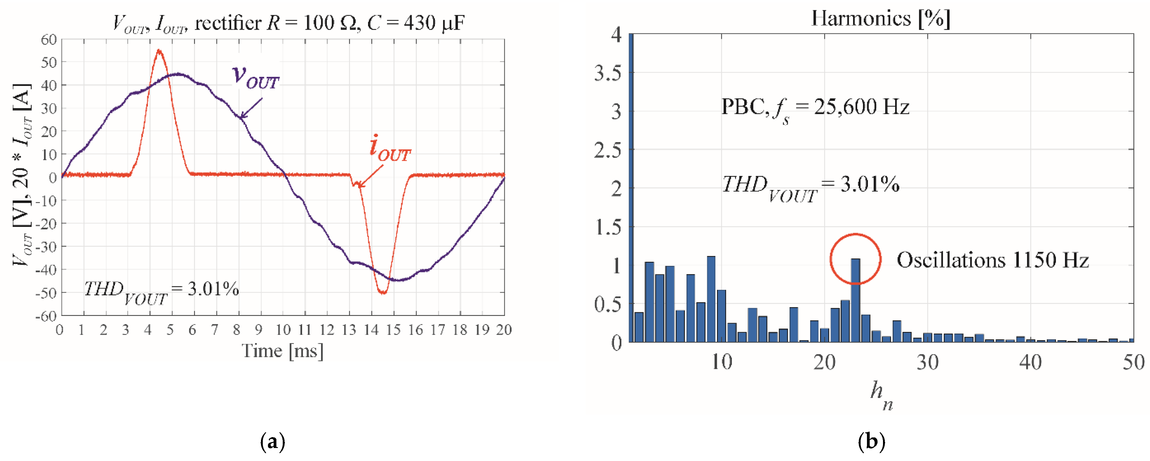
25600 [Hz], Ri = 3, Kv = 0.5
Ri’ = 5.49, Kv’ = 0.92
Border gains3.01%-5.5%
51200 [Hz], Ri = 3, Kv = 0.5
Ri’ = 10.98, Kv’ = 1.83
Border gains2.53%-5%
51200 Hz, Ri = 3, Kv = 0.7
Ri’ = 10.98, Kv’ = 2.56
Above the border values2.62%18.6%3.5%
Publisher’s Note: MDPI stays neutral with regard to jurisdictional claims in published maps and institutional affiliations.

