Review

A Review of Reduction Methods of Impact of Common-Mode Voltage on Electric Drives

Faculty of Electrical and Control Engineering, Gdańsk University of Technology, 80-233 Gdańsk, Poland
*
Author to whom correspondence should be addressed.
Energies 2021, 14(13), 4003; https://doi.org/10.3390/en14134003
Submission received: 4 June 2021 / Revised: 30 June 2021 / Accepted: 30 June 2021 / Published: 2 July 2021

Abstract

:
In this survey paper, typical solutions that focus on the reduction in negative effects resulting from the common-mode voltage influence in AC motor drive applications are re-examined. The critical effectiveness evaluation of the considered methods is based on experimental results of tests performed in a laboratory setup with an induction machine fed by an inverter. The capacity of a common-mode voltage level reduction and voltage gradient du/dt limitation is discussed to extend motor bearings’ lifetime and increase motor windings’ safety. The characteristic features of the described solutions are compared and demonstrated using laboratory results.

1. Introduction

Since the second half of the 20th century, dynamic development of energy conversion methods using power electronic inverters has been observed. As a result, a new generation of electric drives has been developed, whose DC current machines have been replaced by AC current engines (induction and synchronous) supplied by power electronic converters. Thanks to the development of advanced control methods, mechanical variables (torque and angular velocity of the motor shaft) may be fully controlled. Modern electric drives are independent of power source types, and most popular topologies are composed of an indirect frequency converter with a controlled or non-controlled AC/DC converter supplying a DC/AC inverter [1].
In most popular electric drives, basic three-phase full-bridge inverters are commonly used; however, for medium- and high-power applications, multilevel inverters are also applied [2]. Due to the application of fast-switching power transistors, modern variable-frequency drives may operate with carrier frequencies up to 200 kHz [3,4]. It should be noted that, nowadays, a tendency for increasing the switching frequency is still observed, which enables a reduction in system dimensions, in order to increase power conversion density, which allows improving inverters’ operational features. This trend is additionally strengthened by the spreading of modern power electronic switches made with silicon carbide SiC and gallium nitride GaN techniques [5,6].
Despite the unquestionable advantages of conventional two-level bridge inverters (such as simplicity, low cost, various control strategies or susceptibility to modifications), some disadvantages should also be indicated, which are mainly caused by the switch commutation process under non-zero currents and voltages (hard switching). For hard switching conditions, voltage gradients may exceed 10 kV/µs, which results in a high du/dt gradient in the voltage supplying the machine [7]. The long-line effect appears in the wire connecting the motor and inverter. Due to an impedance mismatch between wires and the motor, a wave reflection of the voltage at the line ends occurs (Figure 1) [6,8,9,10]. As a result, a significant overvoltage may be observed at electrical machine terminals, whose level may reach twice that of the inverter’s nominal supply voltage. Hence, the stress on the cables’ and motor windings’ insulation increases, which is the reason for the decrease in the insulation lifetime and reduces the drive’s mean time to failure (MTTF) [6,11,12].
Another consequence caused by applying power inverters in electric drives is the generation of electromagnetic interference emissions (EMI) [13]. It should be noted that the level of generated EMI is one of the main criteria of AC drive inverters’ practical evaluation. As a result of high du/dt gradients, undesirable high-frequency disturbance currents are excited, which may be a significant danger for the electromagnetic compatibility of the environment due to the possibility of interaction through magnetic and capacitive coupling with other elements [14]. Considering the impact of generated disturbances on operational features and the reliability of electric drives, a common-mode EMI reduction is one of the most important challenges accompanying power inverters’ application [15].
The main path of common-mode disturbance currents consists of wires connecting the inverter to the motor and the PE protective ground wire as the return wire (Figure 2) [16,17]. The levels of generated common-mode perturbations are mainly determined by parasitic capacitances between semiconductors and the radiator (usually grounded) [18]. However, parasitic capacitive couplings between semiconductors and the grounded radiator, as well as ground capacitances of DC link buses, Cp1 and Cp2, allow reducing the length of the common-mode currents’ paths to the shortest possible loop, excluding impedance of the supply grid [15].
A high du/dt of the common-mode (CM) voltage slopes excites significant peaks in the leakage current circulating in a PE protective ground wire, which may provoke undesirable operation of residual current circuit breakers, incorrect activation of fire alarms or various sensor operation disturbances [19,20]. It should also be noted that some part of the CM voltage at motor terminals is transferred to a non-grounded motor shaft, which results in an occurrence of a shaft voltage uSH [21]. The shaft voltage influence results at bearing currents’ flow through motor bearings, and, sometimes, these currents are also closed through bearings of the machine loading the motor [22]. The bearing currents cause pits, craters or stripes that appear on the rolling surfaces of bearings, which leads to deterioration of bearings and reduces the MTTF drive factor [18,23]. Especially destructive are electrostatic discharge machining (EDM) bearing currents when insulating lubricating grease films in rotating bearings are broken down due to exceeding the maximum withstand value by the machine shaft voltage [24]. It should be noted that the probability of EDM current occurrence depends on the CM voltage maximum value, and it increases according to the growth of the CM voltage level [25,26].
The aim of this paper is a critical evaluation of selected methods focused on reducing negative effects resulting from CM voltage impact. The comparative evaluation is based on analysis of approaches presented in the literature and experimental tests of the selected solutions. In the first part of this paper, a mechanism of CM voltage generation in an electric drive fed by a conventional two-level bridge inverter is described. Next, a review of methods and experimental results is presented in the form of tables and diagrams to demonstrate the effectiveness of the compared solutions.

2. Mechanism of Common-Mode Voltage Generation in Electric Drive Fed by a Conventional Hard-Switched Two-Level Bridge Voltage Inverter

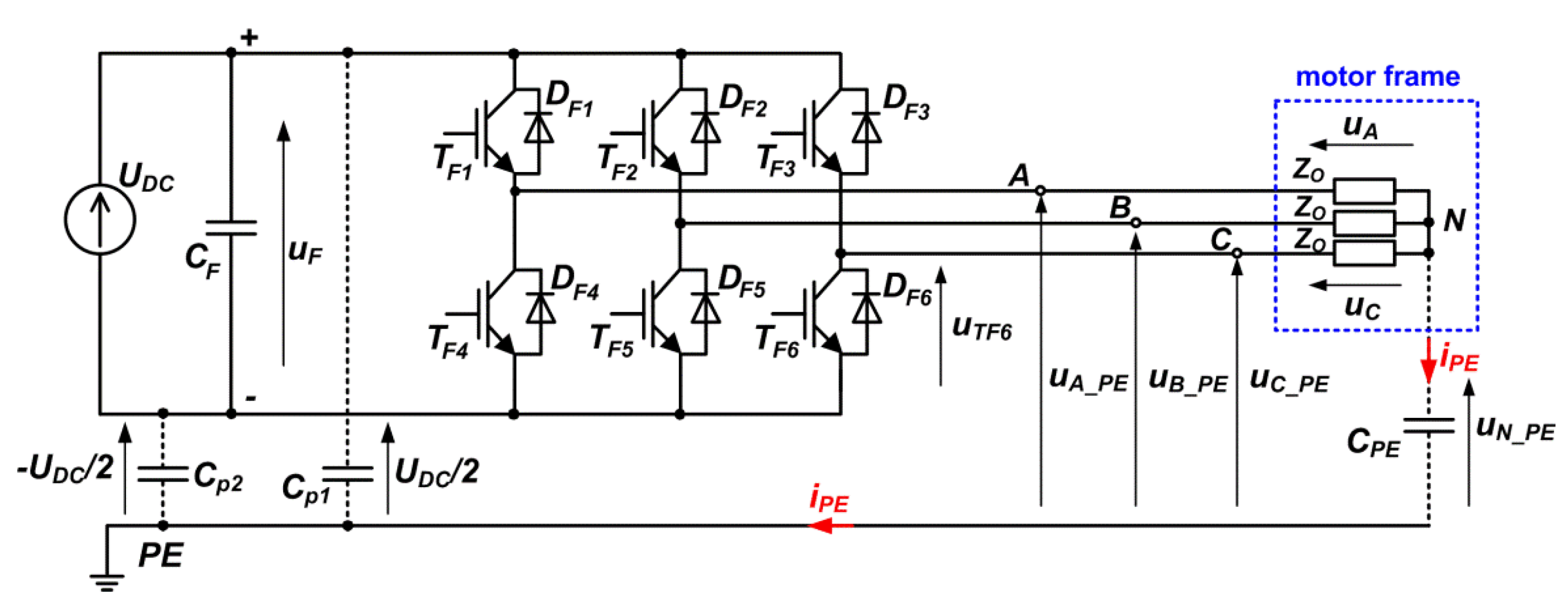
In a hard-switched two-level bridge inverter (Figure 3), due to the application of a high-capacity capacitor CF, the inverter input voltage uF remains constant and is equal to the supply voltage UDC [8]. Assuming that ground capacitance Cp1 = Cp2, the voltage between DC buses and the ground PE equals UDC/2 for a “+” bus and, adequately, −UDC/2 for a “−” bus. The values of inverter output voltages uA_PE, uB_PE and uC_PE are determined by an actual state of inverter transistors TF1TF6, and, exemplarily, for voltage uC_PE, the following relation may be formulated:
u C _ P E = u T F 6 U D C 2
At steady state, voltage uC_PE equals UDC/2 if transistor TF6 is turned off, or uC_PE = −UDC/2 if transistor TF6 is turned on. Analogous relations may be formulated for output voltages uA_PE and uB_PE.
Considering the scheme presented in Figure 3, where motor windings are represented by impedance Zo, the value of a common-mode voltage uN_PE results from
u N _ P E = u C _ P E u C
Moreover, the following relations are also valid:
u A _ P E = u N _ P E + u A ,
u B _ P E = u N _ P E + u B ,
which leads to
u A _ P E + u B _ P E + u C _ P E = 3 u N _ P E + u A + u B + u C .
Assuming symmetry of motor windings’ impedances:
u A + u B + u C = 0 ,
Thus, the common-mode voltage uN_PE is given by
u N _ P E = u A _ P E + u B _ P E + u C _ P E 3
The DC buses’ ground capacitances Cp1 and Cp2 and capacitance CPE (between the grounded motor frame and a neutral point N of star-connected stator windings) form a voltage divider; hence, e.g., for an inverter state of 000 related to TF1, TF2 and TF3, the common-mode voltage uN_PE is described by
u N _ P E = U D C C p 1 C p 1 + C p 2 + C P E .
However, in most cases, it can be assumed that CPE << Cp1 and Cp1Cp2; hence, at steady state, the common-mode voltage uN_PE is only determined by a value of the supply voltage UDC and by a state of inverter transistors TF1TF6. To summarize, for inverter active states uN_PE = ± UDC/6 and uN_PE = ± UDC/2 for the zero vectors 000 and 111.
Considering Equation (1), it can be recognized that the value of derivative duC_PE/dt depends on the rate of change in transistor TF6’s voltage:
d u C _ P E d t = d u T F 6 d t ,
Hence, the value of derivative duN_PE/dt is given by
d u N _ P E d t = d ( u C _ P E u C ) d t = d u T F 6 d t d u C d t .
Considering the scheme presented in Figure 3, the dominant part of a ground leakage current iPE flowing in a PE protective wire from the motor to the inverter is closed in a loop including a motor ground capacitance CPE. Thus, the value of the current iPE is mainly determined by a value of gradient duN_PE/dt, which is correlated with values of derivatives duA_PE/dt, duB_PE/dt and duC_PE/dt resulting from the rate of inverter transistors’ voltage changes. It should also be noted that value of capacitance CPE depends on the motor type, and, typically, for motors with power from 1 to 50 kW, it varies from 2 to 10 nF [27,28].

3. Review of Methods Dedicated to CM Voltage Reduction and Limiting Negative Effects Resulting from uN_PE Voltage Impact

The problem of the measurement and reduction in negative effects resulting from CM voltage impact arose with the dissemination of electric drives fed by voltage inverters. One of the most important aspects affecting the MTTF value of electric drives results from bearing current occurrences in electric machines [19,22]. A shaft grounding, application of conductive greases or dedicated shielded cables, as well as the use of insulated or hybrid bearings, are proposed to reduce bearing currents [22,23,29]. Nevertheless, considering the mechanism of excitation and character of bearing currents, it should be noted that application of one chosen solution may cause a limitation of one type of bearing current and a significant increase in other types of bearing current at the same time (see Table 1) [22]. For example, when one end of the motor shaft is grounded via a brush, EDM currents may be completely reduced; however, the possibility of rotor ground current excitation increases if a non-insulated clutch is applied between the motor and load.
A complete reduction in bearing currents is only provided when relatively expensive hybrid bearings with ceramic rolling elements (Figure 4a) are applied at both ends of the motor shaft. It must be also noted that application of insulated bearings with an insulating layer placed at the outer bearing surface (Figure 4b) results in a partial reduction in EDM currents—about 40 to 60% [22,23].
It should be noted that those solutions depicted in Table 1 do not affect the primary source of bearing currents, which is a CM voltage excited by an inverter. In the considered inverter system, the highest possibility of destructive EDM current excitation occurs for inverter zero states 000 or 111 when the uN_PE voltage reaches its maximum values. Hence, the possibility of a reduction in EDM current occurrence is only possible when the amplitude of the CM voltage is efficiently limited. Basing on the literature review, some exemplary solutions may be specified. In [8,30], specially dedicated active zero voltage control (AZVC) modulation methods were proposed in which two opposite active vectors with exactly the same duration are applied instead of inverter zero vector 000 or 111 (Figure 5). Theoretically, the application of the AZVC method enables a reduction in uN_PE voltage maximum levels to ±UDC/6. However, if inverter transistors are switched in two different branches at the same time, undesirable spikes, whose amplitude exceeds ±UDC/2, may then be noted in the CM voltage waveforms [30]. Moreover, the application of the AZVC method may decrease the quality of the motor current [8]. Another modification of the modulation technique focused on CM voltage reduction is based on using the tri-carrier PWM method with a fixed or adaptive carrier phase displacement angle [31,32]. As a result, significant suppression of the CM voltage harmonic at the carrier frequency is reported, and uN_PE voltage levels may be effectively reduced to ±UDC/6. Additionally, a 50% reduction in the leakage ground current may be achieved; however, an increase in the motor current THD is a negative effect of the applied method [32]. Moreover, significant modifications of inverter control algorithms are needed. It is worth mentioning that similar works have also been carried out for multilevel inverters [33].
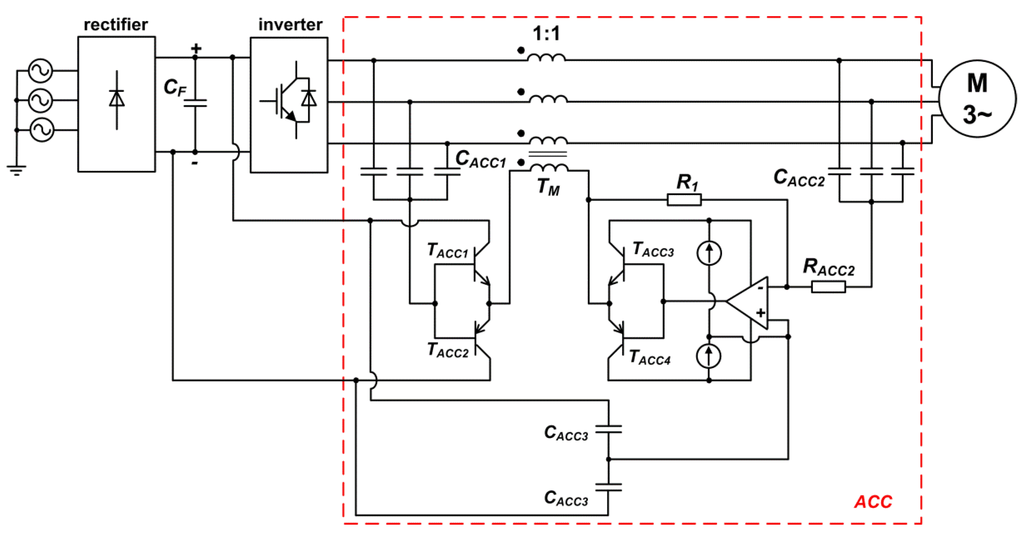
Another approach is based on using specially dedicated active common noise canceller circuits (ACCs) [34,35]. In ACCs, the reduction in CM voltage levels is ensured by the formation of an appropriate compensation voltage, which is added to the phase voltages through a transformer TM placed between the motor and inverter (Figure 6) [36]. The solution provides a reduction in uN_PE voltage levels of more than 90% regardless of the inverter transistors’ state [34]. Additionally, if an ACC operates in a configuration with an active common-mode filter, 20 dB of the average CM voltage attenuation for a frequency higher than 10 MHz is reported [36]. However, the four windings’ transformer TM should be capable of operating with a high switching frequency which significantly increases the complexity of the system. As a result, the application of Mn-Zn ferrite as the magnetic core of the transformer is proposed to ensure CM voltage suppression in a range of frequencies up to several MHz [36]. It should also be noted that application of an ACC requires access to both DC link buses between the rectifier and inverter. In the case of commercially available high-integrated devices, this requirement is often difficult to realize because manufacturers do not usually make these terminals available to users.
If a three-phase motor M is equipped with open stator windings, it may be fed by a dual two-level inverter in the configuration of inverters X and Y, which are supplied by voltage source UDC (Figure 7) [37,38]. In the presented configuration, a zero voltage vector is formed as a combination of opposite active vectors generated by inverters X and Y. A full synchronization between inverter X’s and inverter Y’s transistors’ switching moments should be ensured to provide proper operation of the solution. As a result, control systems and control algorithms become complicated. As it is reported in [39], the presented solution ensures CM voltage maximum level suppression to ±UDC/3; however, due to the high complexity, it is not widely used in practical applications.
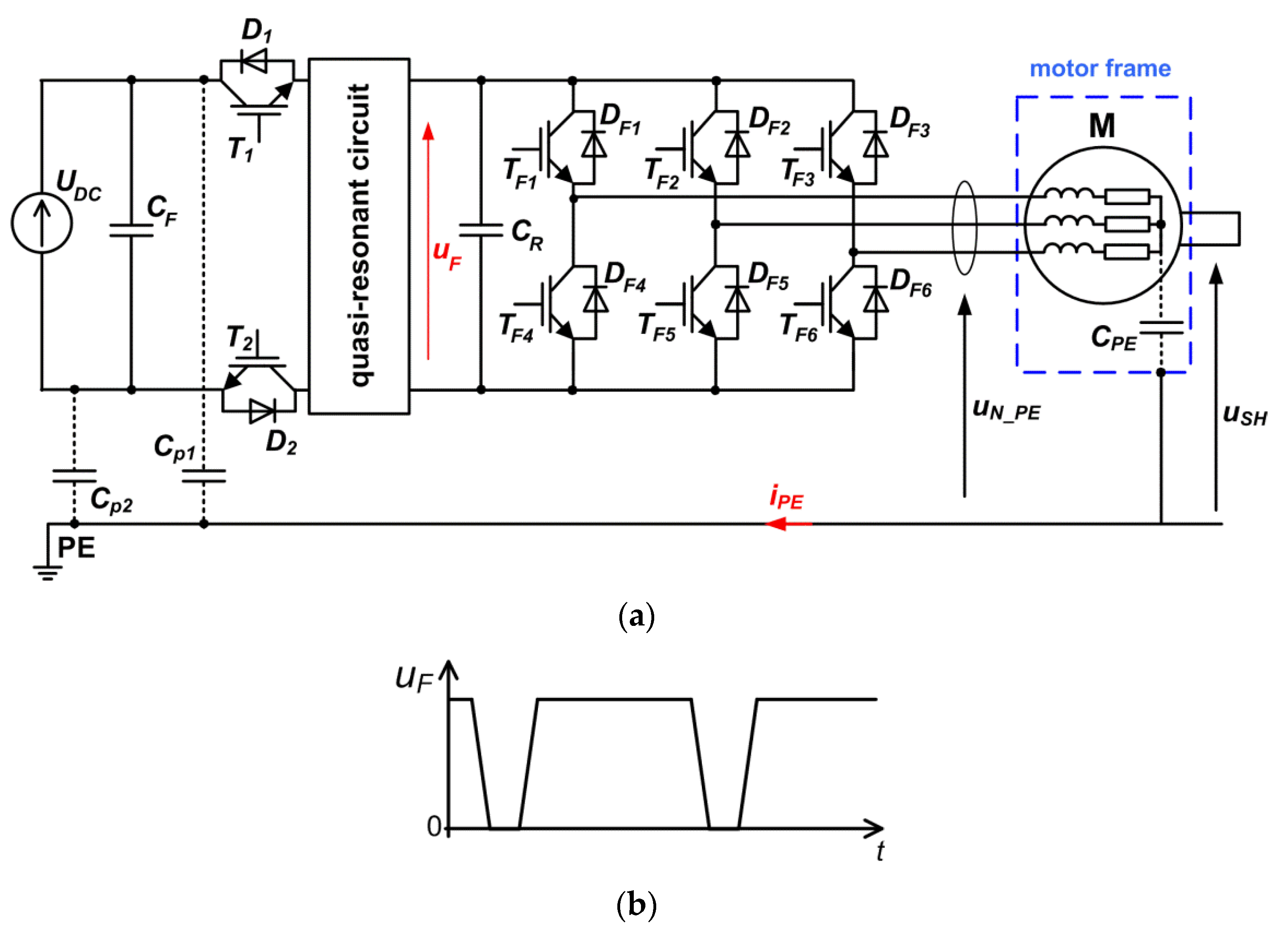
Interesting results are found when a soft-switched inverter is used to feed an electric machine. In such inverters, additional resonant circuits are used to ensure switching transistors under zero voltage (ZVS) or zero current conditions (ZCS) [40]. In comparison with hard switching, soft switching results in reduced du/dt and di/dt gradients of voltages and current waveforms during commutation processes, which enables the limitation of the duN_PE/dt value below 500 V/µs. Parallel quasi-resonant DC link inverters (PQRDCLI) with a quasi-resonant circuit placed between the inverter and supply source UDC seem to be an especially attractive alternative for a basic two-level bridge inverter (Figure 8a) [41]. As a result of the resonant process, the inverter input voltage uF is periodically reduced to zero to form zero voltage notches, which provides ZVS conditions of all inverter transistors (Figure 8b). In PQRDCLI, a quasi-resonant circuit is activated only during the inverter’s main transistors’ switching processes, and it becomes inactive for the rest of the time [41]. This allows reducing the total power losses generated and the EMI level in a quasi-resonant circuit and enables implementation of control methods based on SVPWM modulators, which are widely used in hard-switched inverter control algorithms [42].
In [20,43], PQRDCLI topologies with two insulating switches T1,D1 and T2,D2 placed in DC link buses were presented, which ensures separation of the motor from the supply voltage UDC during inverter transistors’ switching (Figure 8a). As a result, CM voltage levels are limited to ±UDC/6 (in comparison to ±UDC/2 for a hard-switched inverter); hence, the maximum levels of the motor shaft are also significantly reduced, which decreases the possibility of EDM current occurrence. It should also be noted that the ground leakage current iPE and shaft-grounding current at PQRDCLI operation are also limited (by about five times in comparison with a hard-switched inverter). As it is reported in [20,44], in comparison with a hard-switched inverter, a reduction in the du/dt gradient during switching processes in PQRDCLI results in a decrease in the generated conducted disturbances, especially in the range of frequencies from 0.6 to 15 MHz. However, the higher PQRDCLI topology complexity, which results in more complicated control algorithms and an increase in costs, is the main disadvantage of soft-switched inverters. Moreover, further works are still necessary to optimize component parameters of the quasi-resonant circuits that should improve the energy efficiency of the considered solutions. It should also be noted that the common use of modern semiconductors produced with wide-gap materials may encourage further wider practical use of soft-switched inverters due to the limitation of problems resulting from the fast switching of transistors [45].
One of the basic methods focused on reducing negative effects resulting from CM voltage impact is the application of passive filters. This approach is relatively simple, and its adoption into electric drives does not require any modification of the inverter construction, which is often needed if more advanced solutions are implemented [46]. Hence, using the additional motor chokes, the sine-wave filters, the du/dt chokes and the common-mode chokes is the most popular solution met in commercial applications. It should be noted that these techniques do not require any modifications of the motor construction, and hence they can be applied to various motor types.
Due to the low complexity, additional motor chokes installed between the motor and inverter are willingly used (Figure 9). This solution enables smoothing the motor current and a reduction in du/dt voltage gradients at the motor terminals. The inductance of motor chokes depends on the motor power, and it varies from tens of µH for high-power drives to a single mH for low-power applications. It is worth mentioning that a permissible fundamental frequency voltage drop at the motor choke inductance LD at rated load conditions should not exceed 5% [8].
The typical sine-wave filters are low-pass LC filters (Figure 10) smoothing inverter output voltage waveforms, which enables forming motor currents and voltage waveforms to a near sinusoidal profile. The most popular topology of the sine-wave filter is composed of inductors LS and star-connected capacitors CS, as presented in Figure 10 [5,47]. It is worth mentioning that more complicated solutions with an increased number of inductors; with a neutral point of capacitors CS connected alternatively to inverter DC buses or to a midpoint of capacitors forming the DC link; or with a neutral point grounded are also proposed [27,48,49]. However, these solutions are more complicated, and their application often requires intervention in the internal inverter construction.
Considering the sine-wave filter topology as it is presented in Figure 10, inductance LS forms a resonant circuit with filter capacitance CS, whose resonant frequency fr is given as follows [5]:
f r = 1 2 π L S C s
Filter parameters must be selected to meet the following requirements:
f o u t f r f s w ,
where fout is a fundamental output frequency and fsw is a switching frequency resulting from the carrier frequency. If the resonant frequency fr is significantly lower than frequency fsw, additional damping resistors do not have to be applied because some damping is achieved by the loss in the filter inductor LS core. From Equation (11)’s results, inductance LS should be large to reduce capacitance CS; however, its maximum value is limited by a permissible fundamental frequency voltage drop (it should be less than 5%). The proposed sine-wave filter design methods are usually based on analysis of inverter transistors’ switching frequency; nevertheless, methods basing on the analysis of the motor impedance are also described [5]. A typical value of inductance LS varies from hundreds of µH to several mH, and the value of capacitance CS reaches several µF.
Comparing with motor chokes, the cost of sine-wave filters is higher. Moreover, implementation of a sine-wave filter requires modification of a motor control algorithm due to the introduction of an additional phase shift between voltages and motor currents by the filter [50]. It should also be noted that the application of sine-wave filters results in additional power loss generation on filter elements, which may be significantly higher than reported for other solutions [5,51].
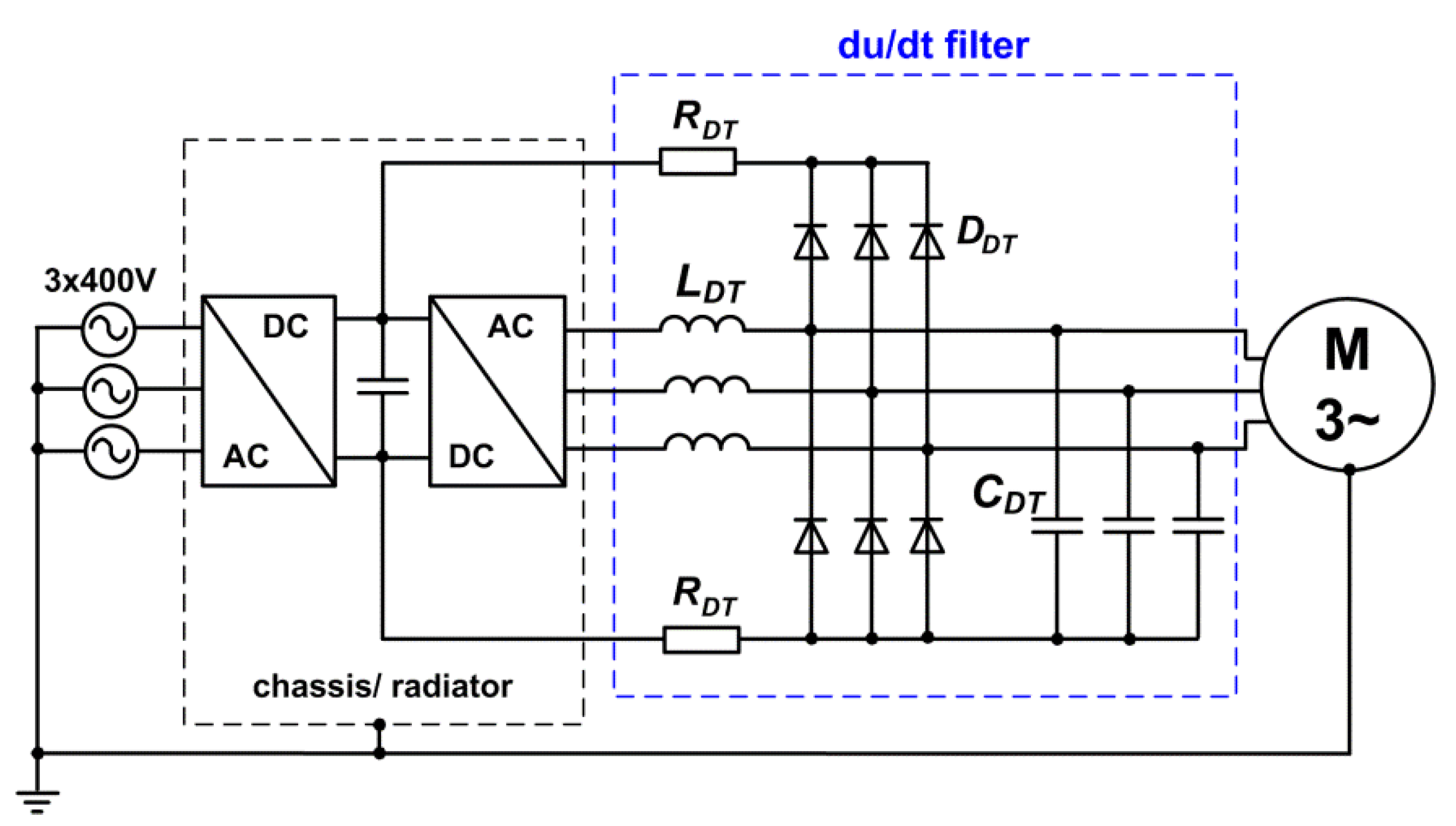
The main task of the du/dt chokes installed between the motor and inverter is the reduction in du/dt voltage gradients affecting the motor. The inductance of the du/dt chokes is significantly lower than that of motor chokes or sine-wave filters, and it ranges from a single µH to hundreds of µH. If wires connecting the inverter and motor are long (more than 10 m), application of specially dedicated du/dt filters is also proposed [6,7]. Such filters are composed of a passive LC filter and an overvoltage reduction circuit [52] (Figure 11). Values of inductance LDT and capacitance CDT are lower than in sine-wave filters, which results in a lower cost and smaller dimensions. Application of du/dt filters enables a reduction in the du/dt gradient of less than 400 V/µS and limiting overvoltage to 1.3∙UDC [52,53]. However, practical implementation of du/dt filters requires access to both DC link buses of the inverter, which, in many commercial devices, cannot be ensured. Hence, in comparison with other simpler solutions, the usability of du/dt filters is limited.
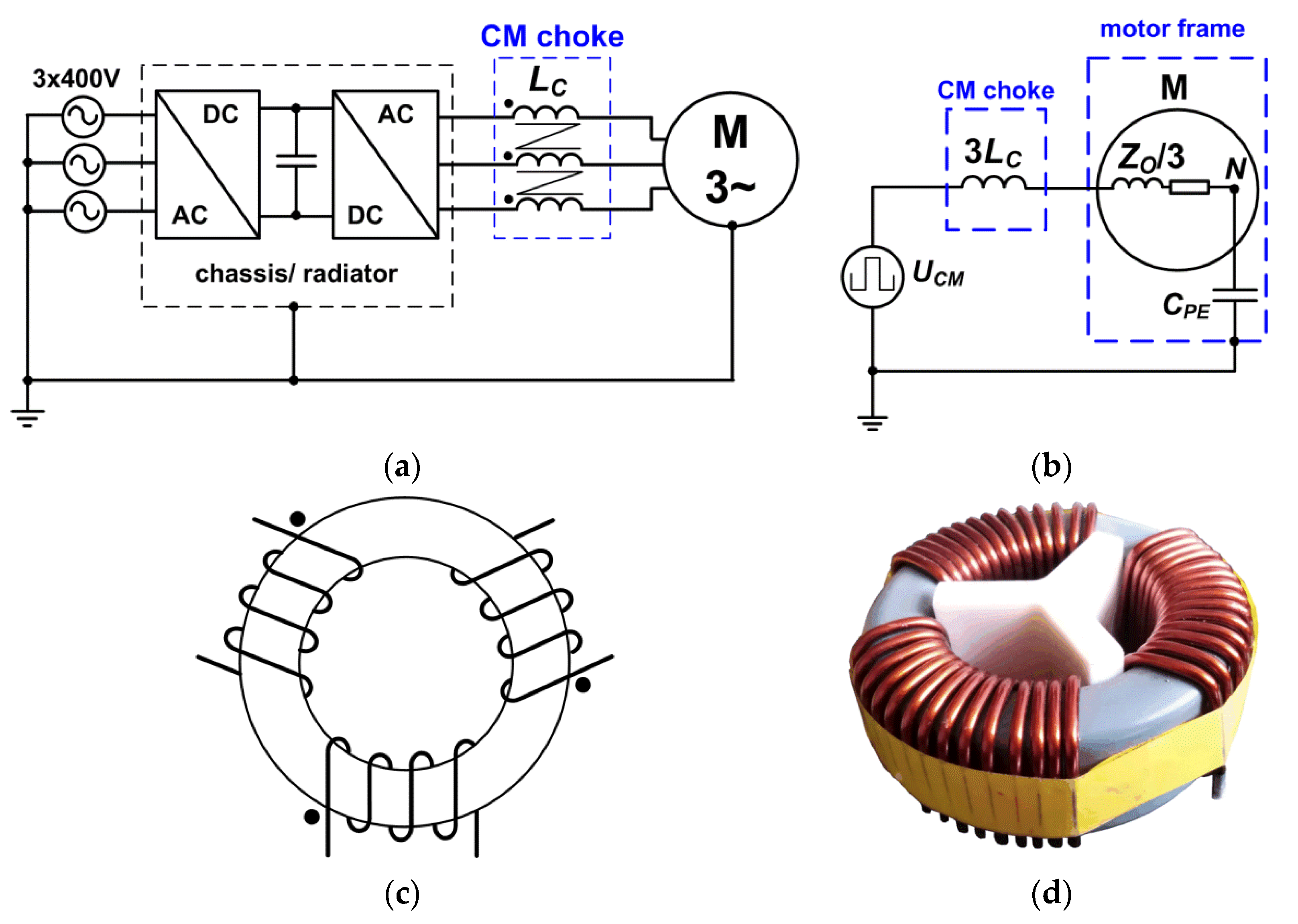
In order to reduce common-mode current values, common-mode (CM) chokes installed between the motor and inverter are widely used (Figure 12a) [8]. A CM choke introduces additional impedance in the common-mode disturbance currents’ flow loop between the motor and a common-mode voltage source UCM (inverter), which results in a reduction in CM (Figure 12b). Three-phase CM chokes are composed of three symmetrical windings wound on a common core—usually, toroidal cores are used (Figure 12c) [54]. The mutual inductance between each winding is identical. For symmetrical three-phase currents flowing between the motor and inverter, a resultant flux in a CM choke core is zero; hence, in that case, CM choke impedance may be neglected [8]. As a result, CM chokes do not take part in differential-mode disturbance reduction. The CM choke parameters should be fitted to avoid saturation of the core by the current flowing through the windings [3,55]. It should also be noted that the problem of CM choke design is still actual, and it is discussed in many papers [3,17,54].

4. Experimental Results

The effectiveness of the most popular selected solutions basing on alternative application of a motor choke, a du/dt choke, a CM choke and a sine-wave filter (in the configuration presented in Figure 10) was verified experimentally in a laboratory setup with a 7.5 kW induction motor type Sg132 M4 fed by a commercial inverter, Parker AC10 10G-44-0170-BF (7.5 kW, 17A, 3 × 400 V). The parameters of the used chokes and filter were fitted to the motor and inverter requirements according to procedures described in application notes and the available literature [8].

4.1. Common-Mode Impedance Characteristics

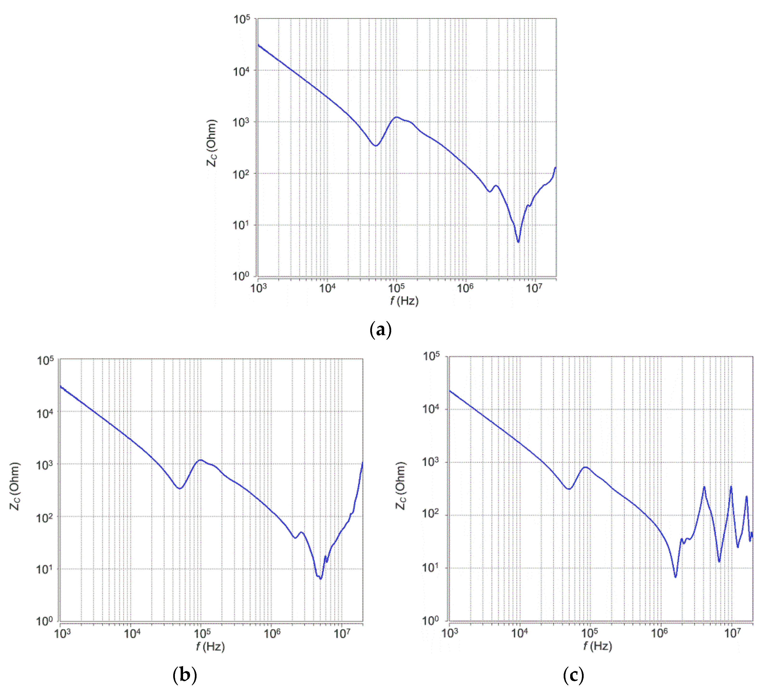
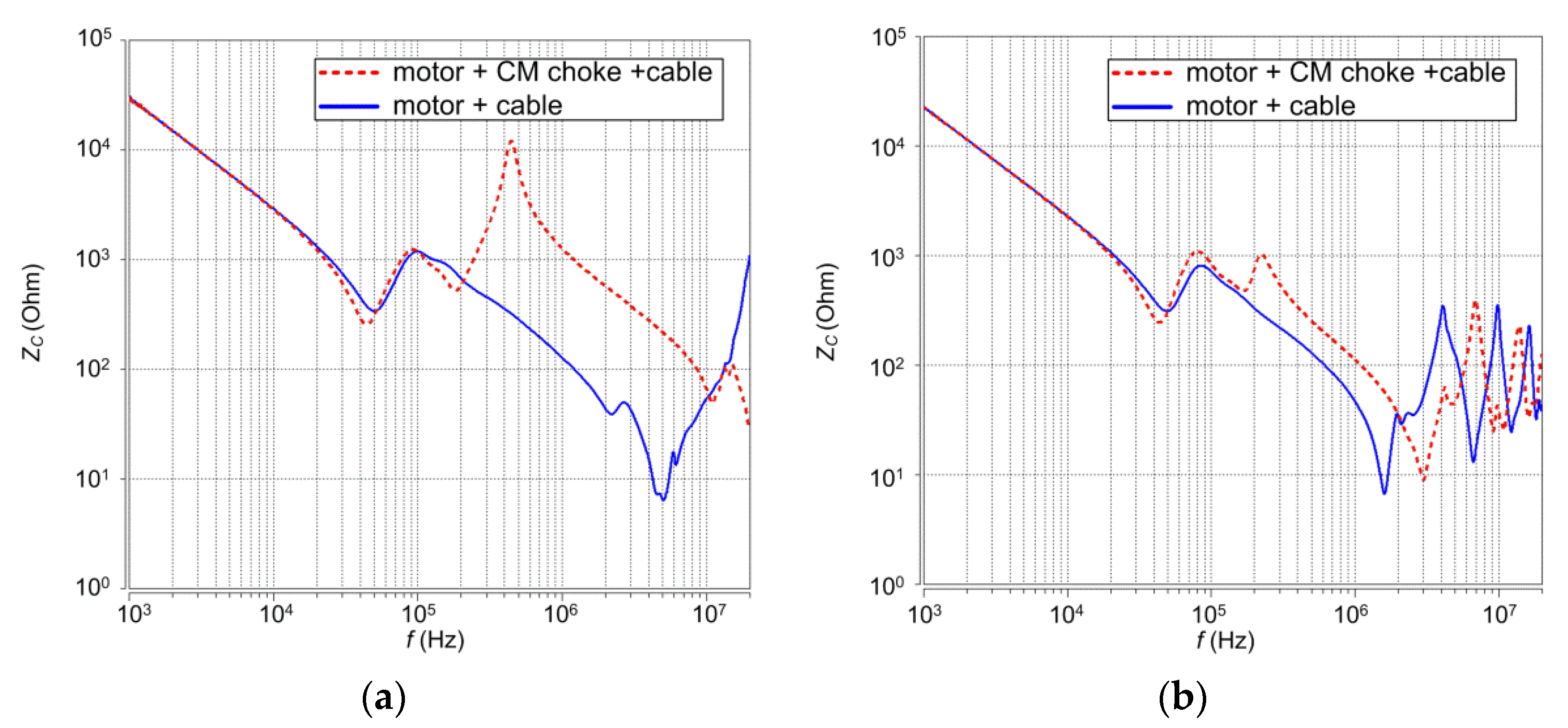
Installation of a filter or chokes between the inverter and motor affects the impedance of the common-mode disturbances’ main propagation path. The common-mode impedance ZC frequency characteristics of a circuit composed of a cable, motor and chokes or a filter were obtained using the impedance analyzer Keysight E4990A in the configuration presented in Figure 13. Frequency characteristics ZC(f) were measured between the short-circuited input terminal ABC and a PE protective wire. Two cables of the same type (four wires, non-shielded) but different lengths (1 m and 10 m) were applied during the performed test.
At the first step, a motor common-mode impedance characteristic was measured. As it is presented in Figure 14a, the impact of motor capacitive components is distinguishable in almost the full considered range of frequencies, with a dominant impact of capacitance CPE between the stator windings and grounded motor frame in a range of frequencies up to 50 kHz. An impact of cable parasitic components is especially recognized at a higher frequency range (more than 2 MHz), and it increases with the cable length, which results in the appearance of additional resonances (Figure 14b,c).
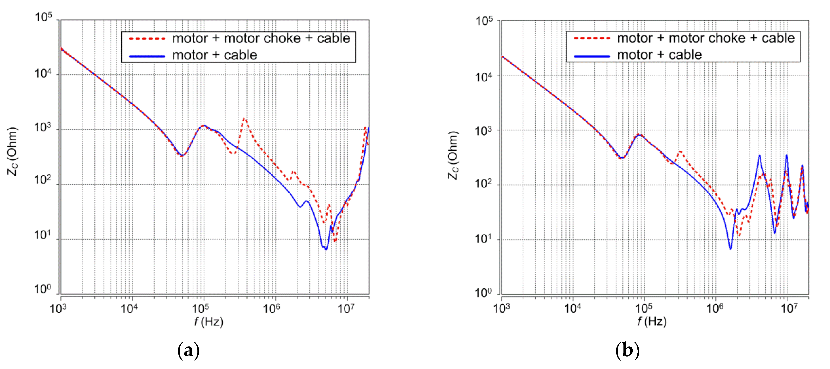
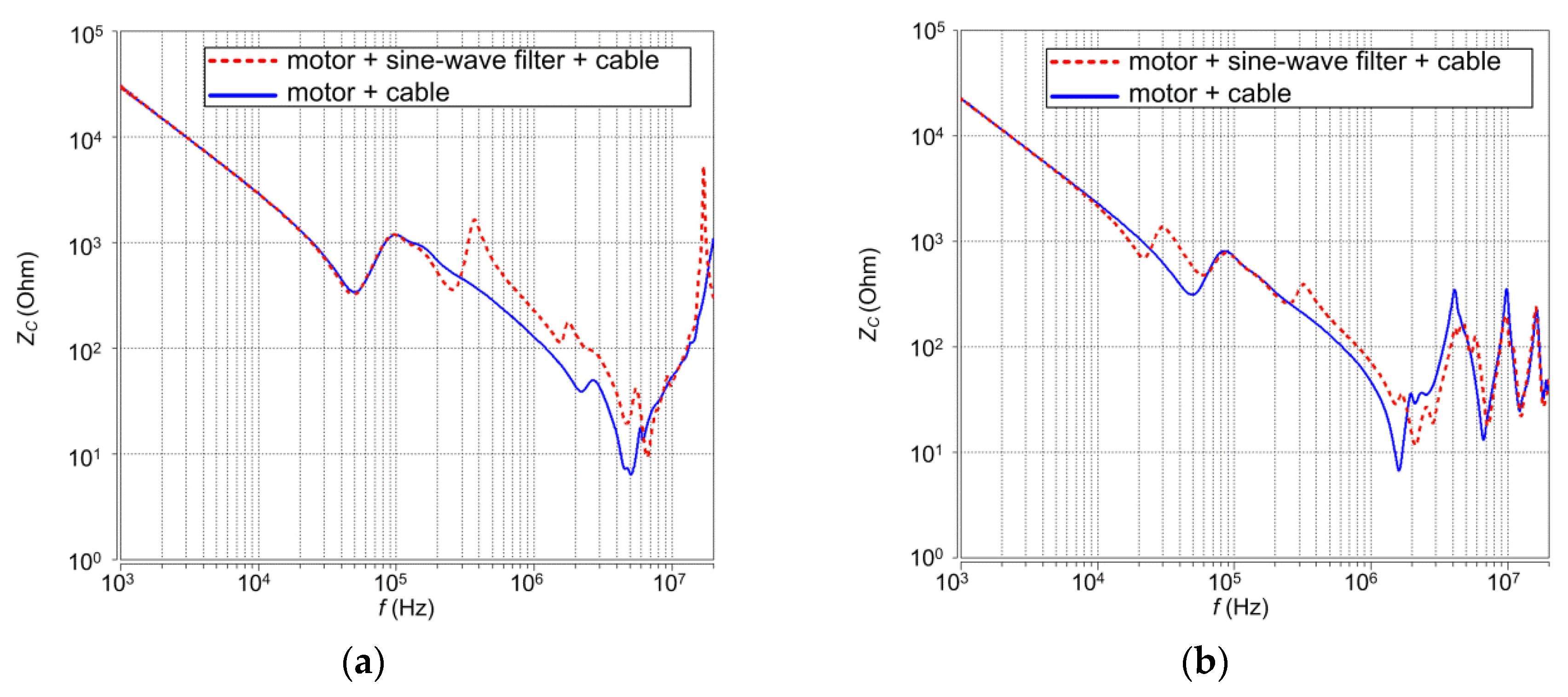
The application of the du/dt choke LDT = 0.31 mH type 3RTU-21 (Trafeco) does not affect the impedance ZC(f) characteristics in the frequency range up to 500 kHz regardless of the cable length (Figure 15). A left shift in resonant frequencies is noticed at a higher frequency, which results from the additional du/dt choke inductance implemented in the total loop inductance. Using the motor choke (3RTM LD = 3.8 mH/18A, Trafeco) results in a noticeable increase in the ZC impedance value in the frequency range from 300 kHz to 2 MHz (Figure 16). It is worth mentioning that this effect is less visible for a longer cable (Figure 16b). Moreover, additional resonance at the frequency of 300 kHz is also excited for both considered cables’ lengths. Similar results are noticed when the sine-wave filter composed of an inductor LS = 3.8 mH and a capacitor CS = 15 µF is applied (Figure 17). For a 10 m cable, a decrease in resonant frequencies from 50 to 20 kHz and from 90 to 60 kHz is observed, which results from the interaction between the impedances of the filter, motor and cable parasitic components (Figure 17b).
The highest impact on the ZC(f) characteristic is noticed when a CM choke (LC = 0.72 mH) is applied (Figure 18). A distinct common-mode impedance value increase is observed for a frequency higher than 200 kHz; however, this effect is determined by the cable parameters, and it is significantly weakened if the cable length grows. Moreover, the CM choke impedance excites additional resonance with a frequency between 200 and 500 kHz (depending on the cable length), which is especially visible when a 1 m cable is used (Figure 18a).

4.2. Voltage and Current Waveforms

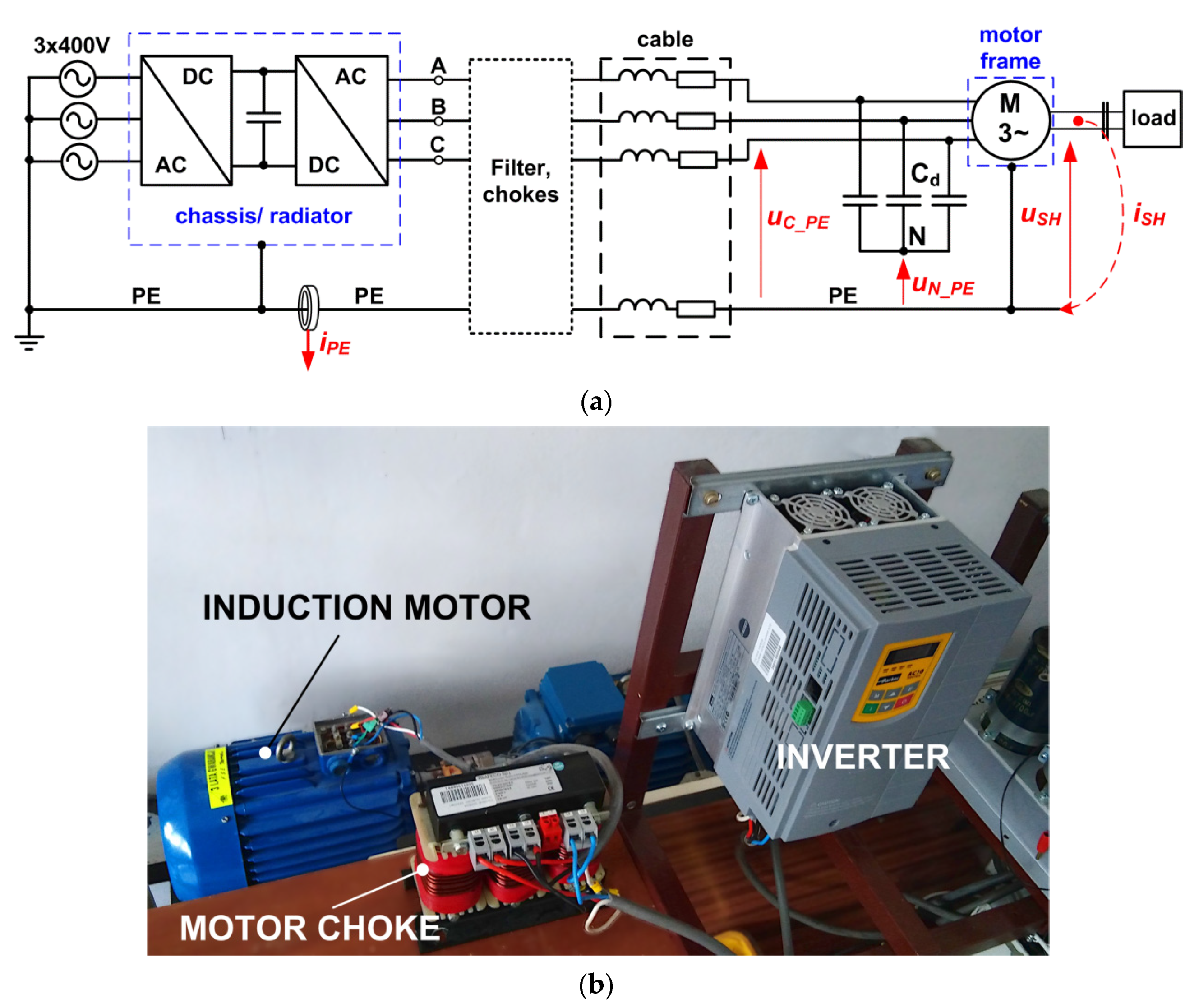
The laboratory setup for experimental tests is presented in Figure 19. The Parker AC10 10G-44-0170-BF (7.5 kW, 17A, 3 × 400 V) inverter was loaded by a 7.5 kW induction motor equipped with hybrid bearings with ceramic rolling elements. Measurement of the motor shaft voltage uSH and shaft current iSH was ensured by using the shaft brush mounted on the motor frame [20]. The motor was loaded by an induction generator, and insulation between the motor and generator was performed by the installation of an insulated clutch. Star-connected capacitors Cd (3 × 680 pF) were used to measure a common-mode voltage uN_PE affecting motor windings. Additionally, a measurement of a phase voltage uC_PE referred to as the PE ground potential was also performed.
The Tektronix DPO4034 oscilloscope equipped with the high-voltage differential probe P5205A (100 MHz) and the current probe TCP2020 (50 MHz) was used to record voltage and current waveforms. Tests were performed under two different cable lengths (1 m and 10 m) and different configurations of filters and chokes installed between the motor and inverter. Configurations with a 3.8 mH motor choke, a 0.72 mH CM choke, a 0.31 mH du/dt choke, a 3.8 mH/15 µF sine-wave filter and a 3.8 mH/15 µF sine-wave filter with a 0.72 mH CM choke were taken into account.
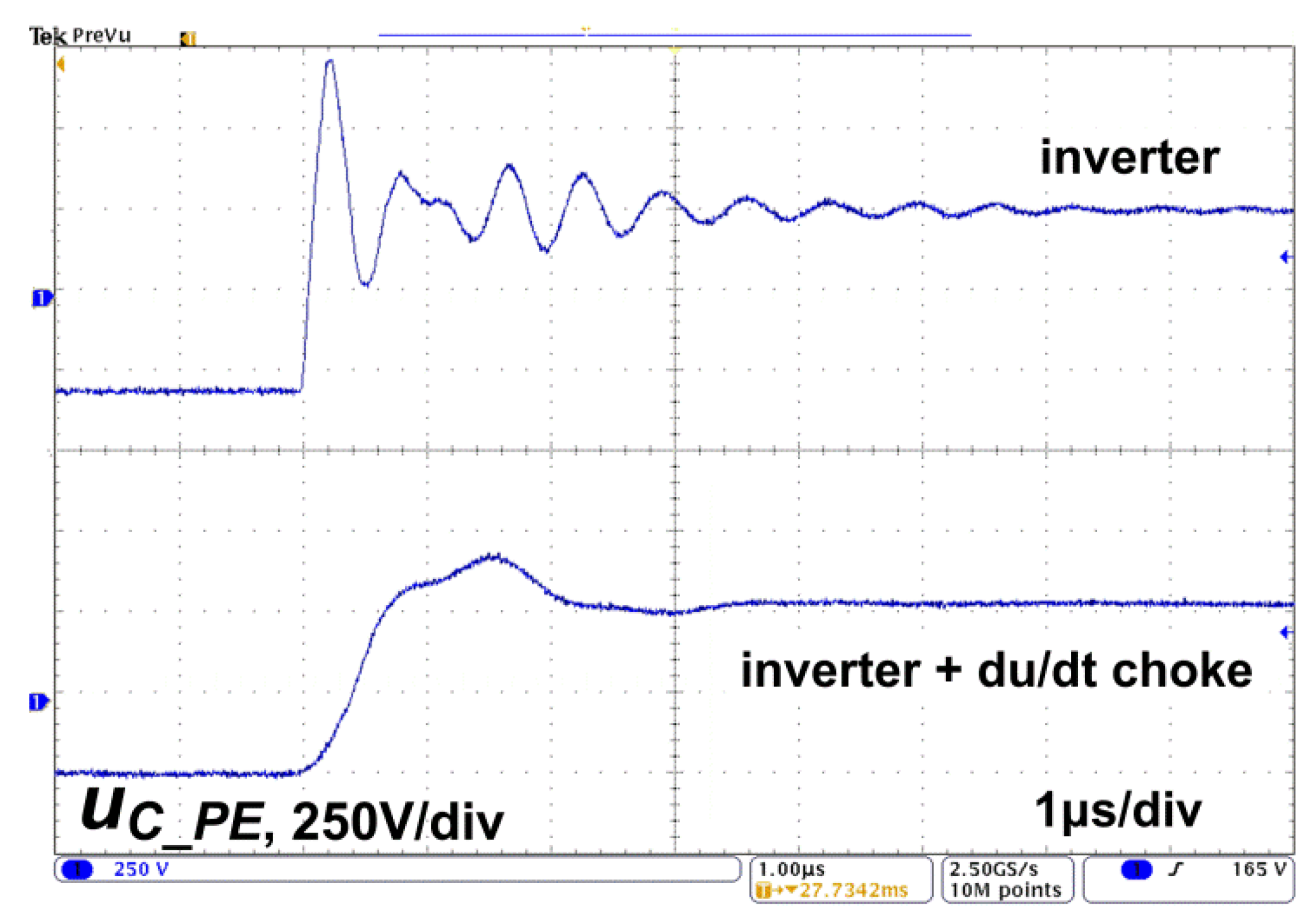
From Equation (3), it can be derived that common-mode voltage uN_PE levels, as well as the duN_PE/dt gradient, are determined by phase voltages uA_PE, uB_PE and uC_PE referring to the PE ground potential. As a result, a reduction in gradient duN_PE/dt (which limits the leakage ground current iPE flowing in a PE protective ground wire) may be achieved by the limitation of derivatives duA_PE/dt, duC_PE/dt and duC_PE/dt. If no countermeasures were used, the value of derivative duC_PE/dt significantly exceeded 5 kV/µs regardless of the cable length (Table 2). It is worth mentioning that gradient duC_PE/dt is lower for a longer cable, which is caused by the additional inductances introduced between the motor and inverter by a longer cable. Application of the CM choke with the sine-wave filter results in the highest reduction in gradient duC_PE/dt (duC_PE/dt << 1 kV/us). A good effect (duC_PE/dt reduced to below 1.3 kV/us) is also noted when only the CM choke is used; however, the effectiveness of the CM choke decreases if the cable length increases. The sine-wave filter and the du/dt choke ensure a comparable level of du/dt reduction, with the duC_PE/dt value limited to 1.6 kV/us (Figure 20). When the motor choke was applied, the lowest level of du/dt gradient reduction was observed (duC_PE/dt reduced to 2.5 kV/us).
Besides the reduction in the du/dt gradient, an impact of the considered solutions on the uC_PE voltage spectrum is also perceptible. In comparison with other solutions, the most significant reduction (of about 25 dBµV) in the uC_PE voltage spectrum was noticed when the CM choke in a configuration with the sine-wave filter was applied (Figure 21i,j). For this configuration, a spectrum limitation was achieved in a range of frequencies higher than 150 kHz regardless of the cable length. If only the CM choke is used, the spectrum is deteriorated due to the appearance of a peak at the frequency of 1.5 MHz, which is about 16 dBµV higher than the one noticed in the configuration with a single inverter (Figure 21g,h). For the rest of the considered solutions, the level of spectrum suppression is comparable.
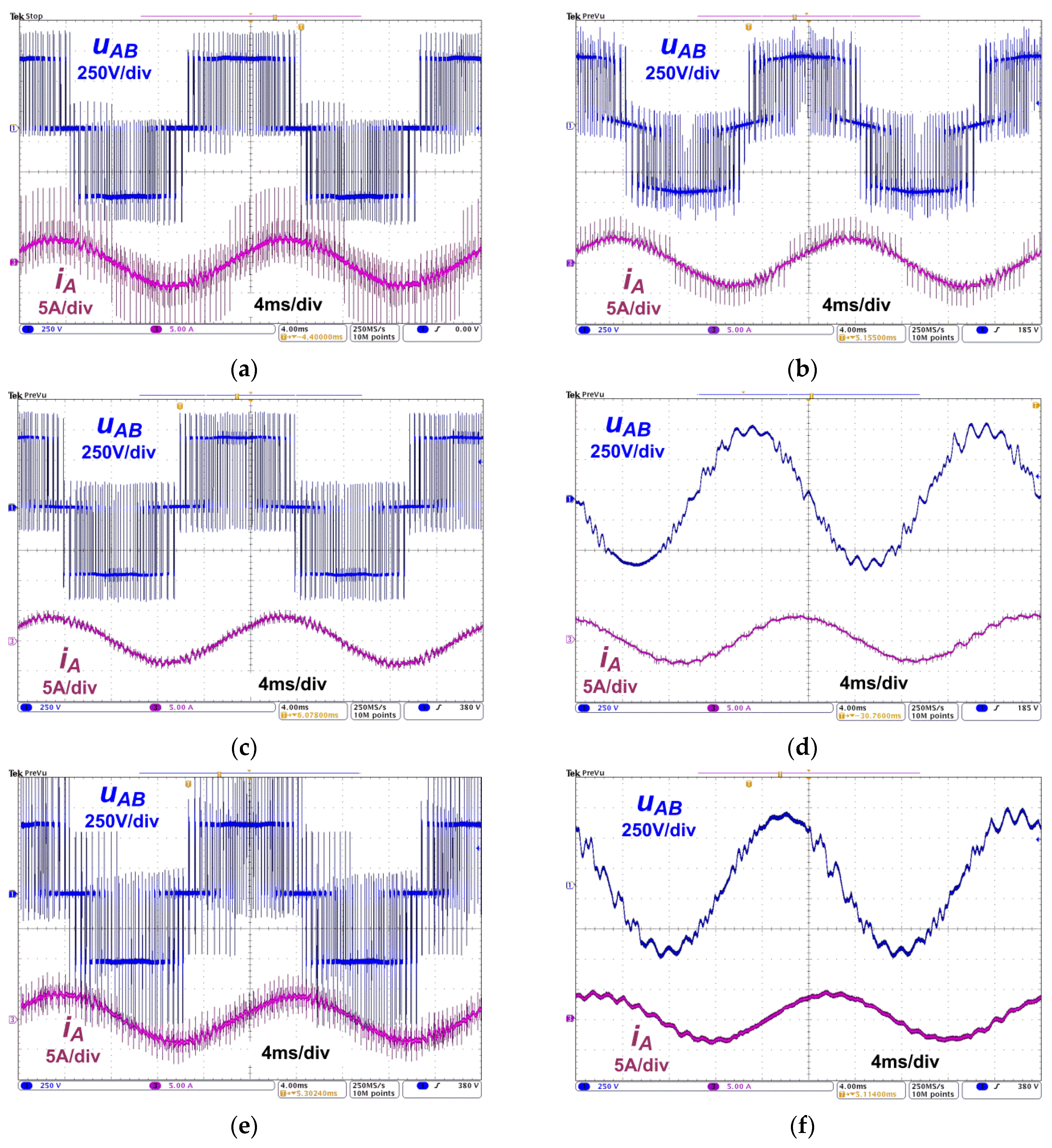
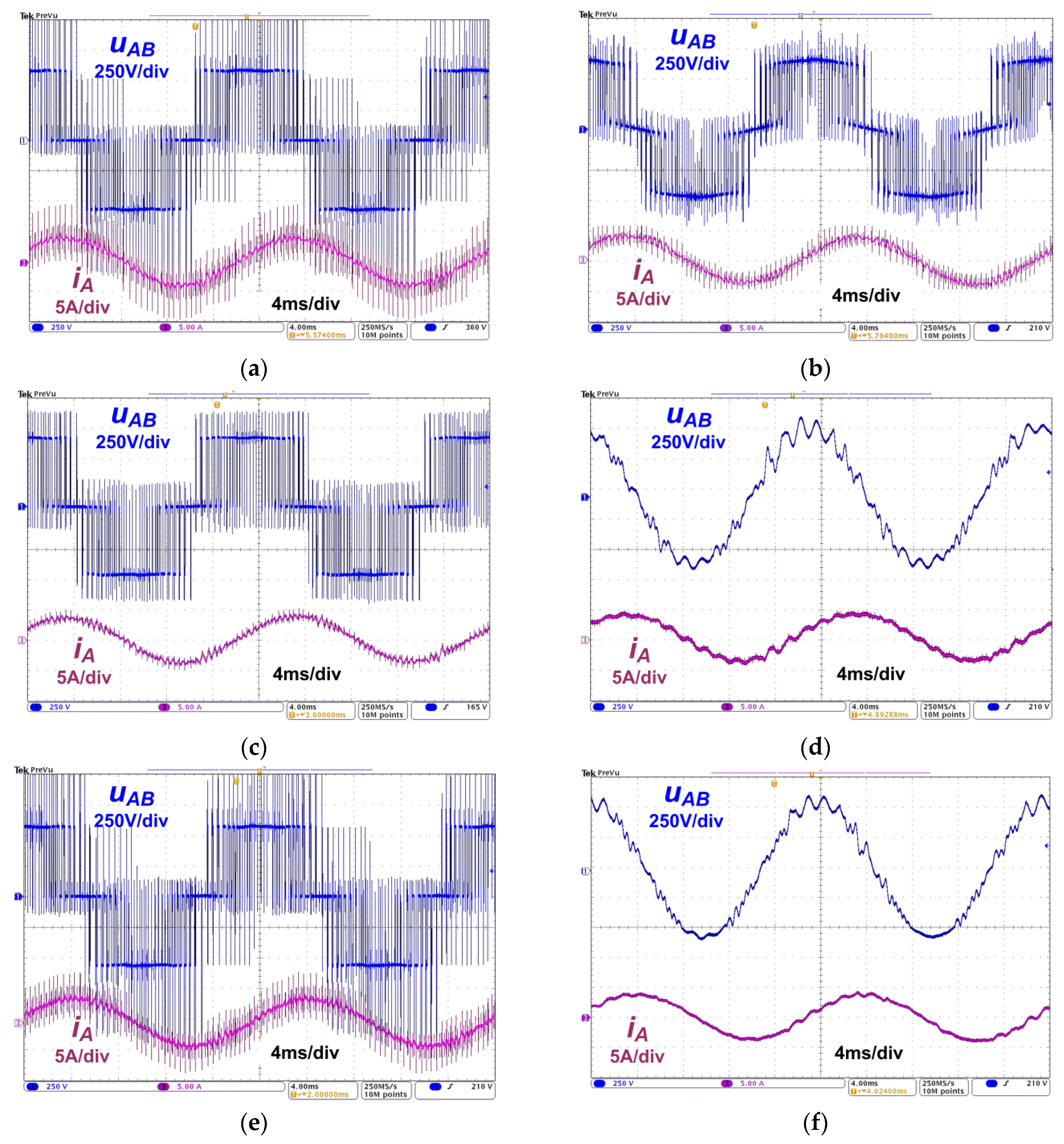
Experimental waveforms of the line-to-line voltage uAB and current iA measured at motor terminals are presented in Figure 22 and Figure 23. High du/dt values in connection with high-frequency wave reflections result in overvoltage spikes’ excitation, whose value may exceed twice that of the DC voltage supplying the inverter (Table 2, Figure 22a and Figure 23a). Hence, a reduction in the du/dt gradient of voltages affecting the motor windings causes a limitation in the overvoltage spikes’ maximal value and decreases insulation voltage stress. Application of the motor chokes or the du/dt chokes does not completely suppress overvoltage spikes, and only a slight reduction in their maximal values is noticed, wherein this effect is more pronounced with a longer cable (Table 2). A complete limitation of the overvoltage spikes is noticed when sine-wave filters are applied (Figure 22d,f and Figure 23d,f). Using the sine-wave filters brings the voltage waveforms to a near sinusoidal shape without significant overvoltage spikes. Smoothing of voltage waveforms also enables an improvement in the motor current shape. It should also be noted that using the CM choke does not suppress overvoltage spikes from line-to-line voltage waveforms despite the reduction in the du/dt gradient of phase-to-ground voltages. For the differential-mode disturbances, the impedance of the CM choke is small; hence, its influence on differential-mode disturbance reduction is negligible. As a result, the CM choke should be used in a configuration with other solutions (e.g., sine-wave filter) to improve the supply conditions of a motor fed by an inverter (Figure 22f and Figure 23f).
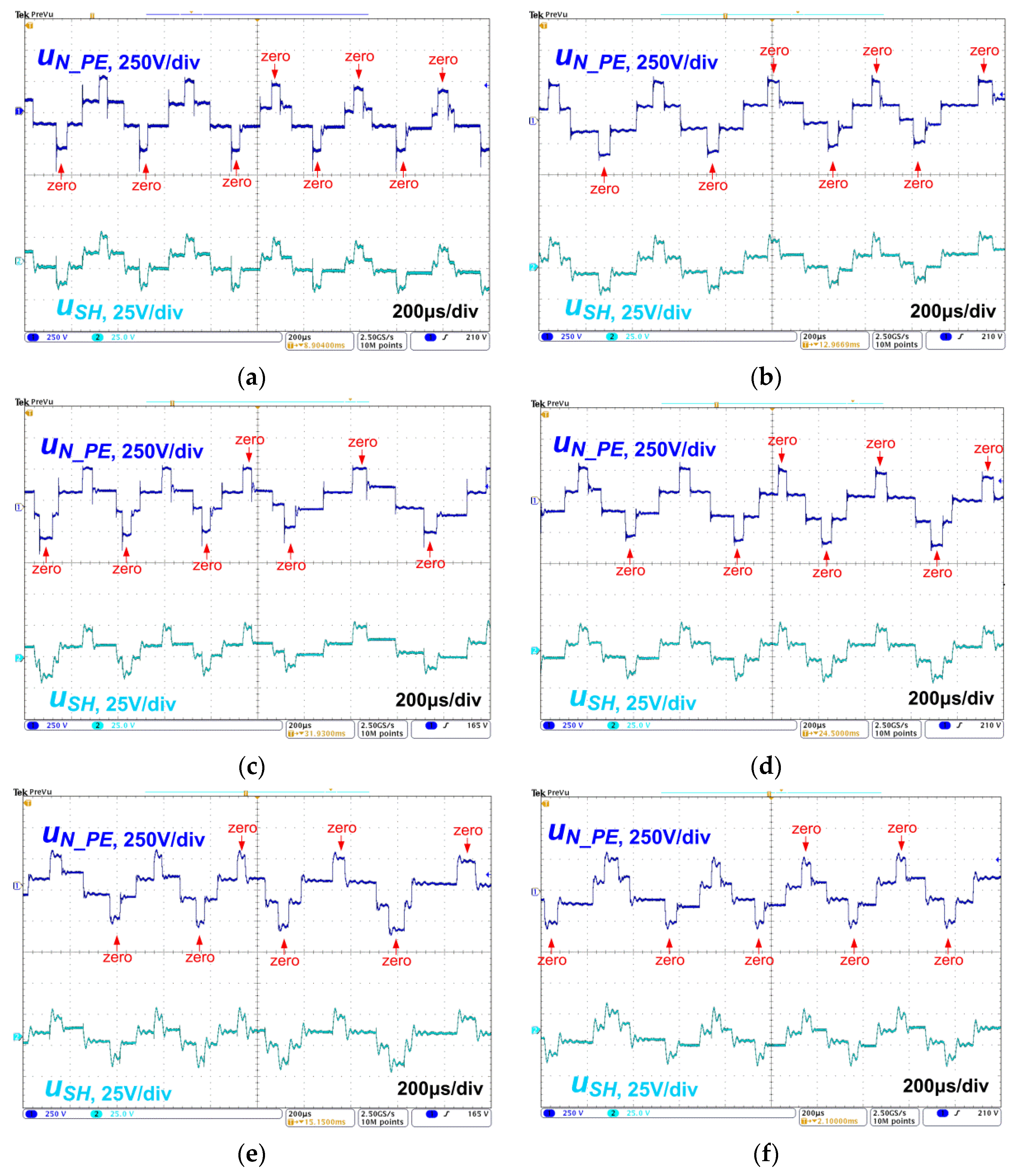
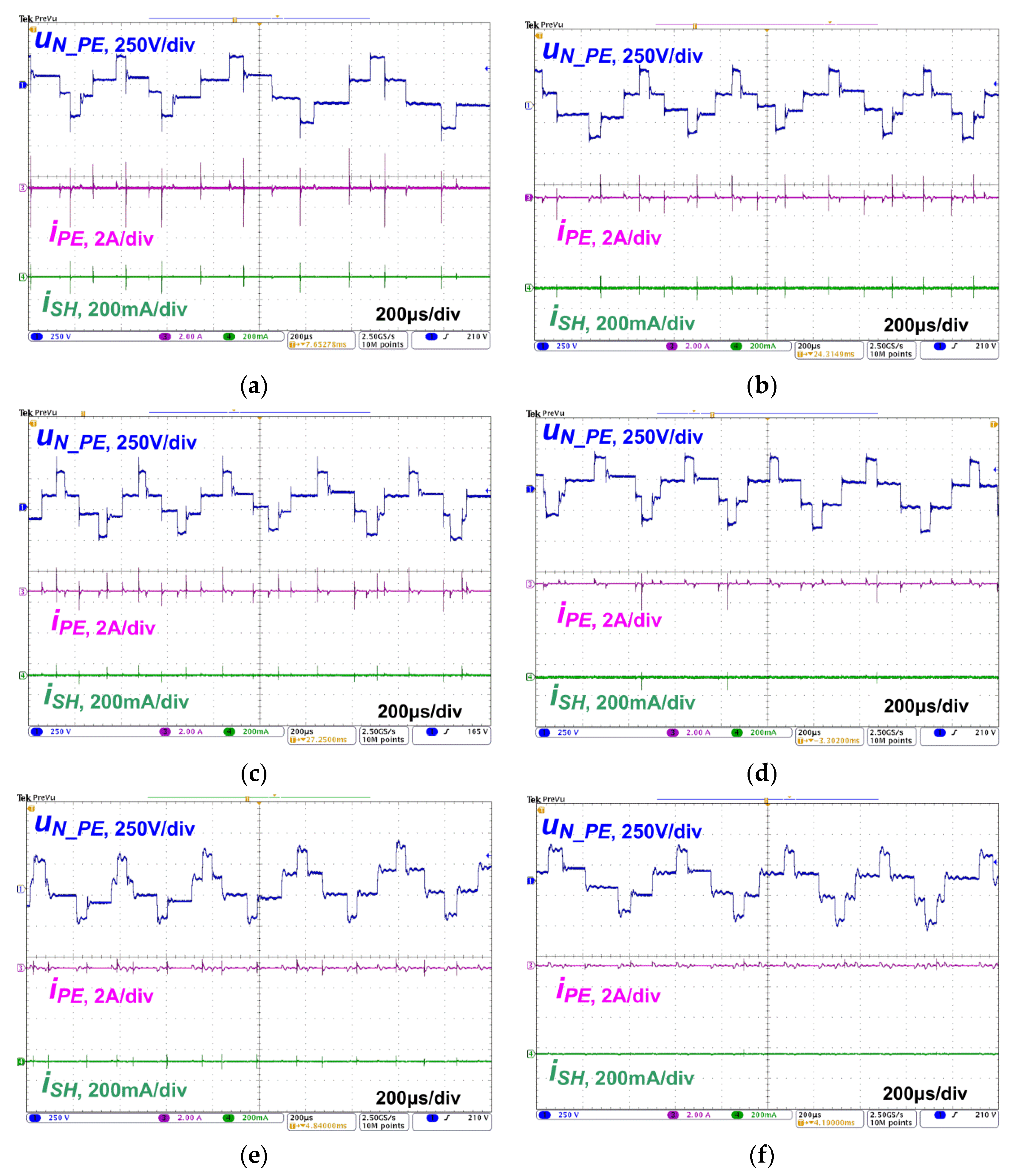
Comparative measurements of the common-mode voltage uN_PE and motor shaft voltage uSH were performed for the considered solutions (Figure 24 and Figure 25). If a conventional two-level inverter is used, the uN_PE voltage equals ±UDC/6 for the active vectors and ±UDC/2 for the zero vectors (Figure 24a and Figure 25a). The shaft voltage uSH reflects the common-mode voltage waveform with the maintenance of the bearing voltage ratio, BVR ≈ 5%, which is a typical value for induction motors. Thus, the possibility of destructive EDM current appearance is the highest for the inverter zero vectors, when the uSH voltage reaches its maximum values. The du/dt gradient of voltage uSH is slightly lower than that observed in uN_PE waveforms, which is caused by an impact of the motor stator windings or shaft motor frame impedances. The presented results of the performed measurements show that none of the comparative solutions ensure a significant reduction in common-mode and shaft voltage levels (Figure 24 and Figure 25).
It is worth mentioning that despite the sinusoidal shape of the line-to-line voltage measured at motor terminals, the considered sine-wave filter does not affect the uN_PE and uSH levels. Considering the equivalent scheme presented in Figure 26, it can be distinguished that the sine-wave filter inductances LS, capacitors CS and Cd and motor ground capacitance CPE form a resonant series circuit LC supplied by a constant DC voltage source. Neglecting the impact of capacitor Cd and the motor impedance ZO, it can be assumed that CS >> CPE, Cp1 = Cp2 and Cp1 >> CPE; hence, the sine-wave filter capacitance CS does not affect the uN_PE voltage levels at a steady state. Similarly, the impact of inductance LS is also omitted in common-mode voltage level forming.
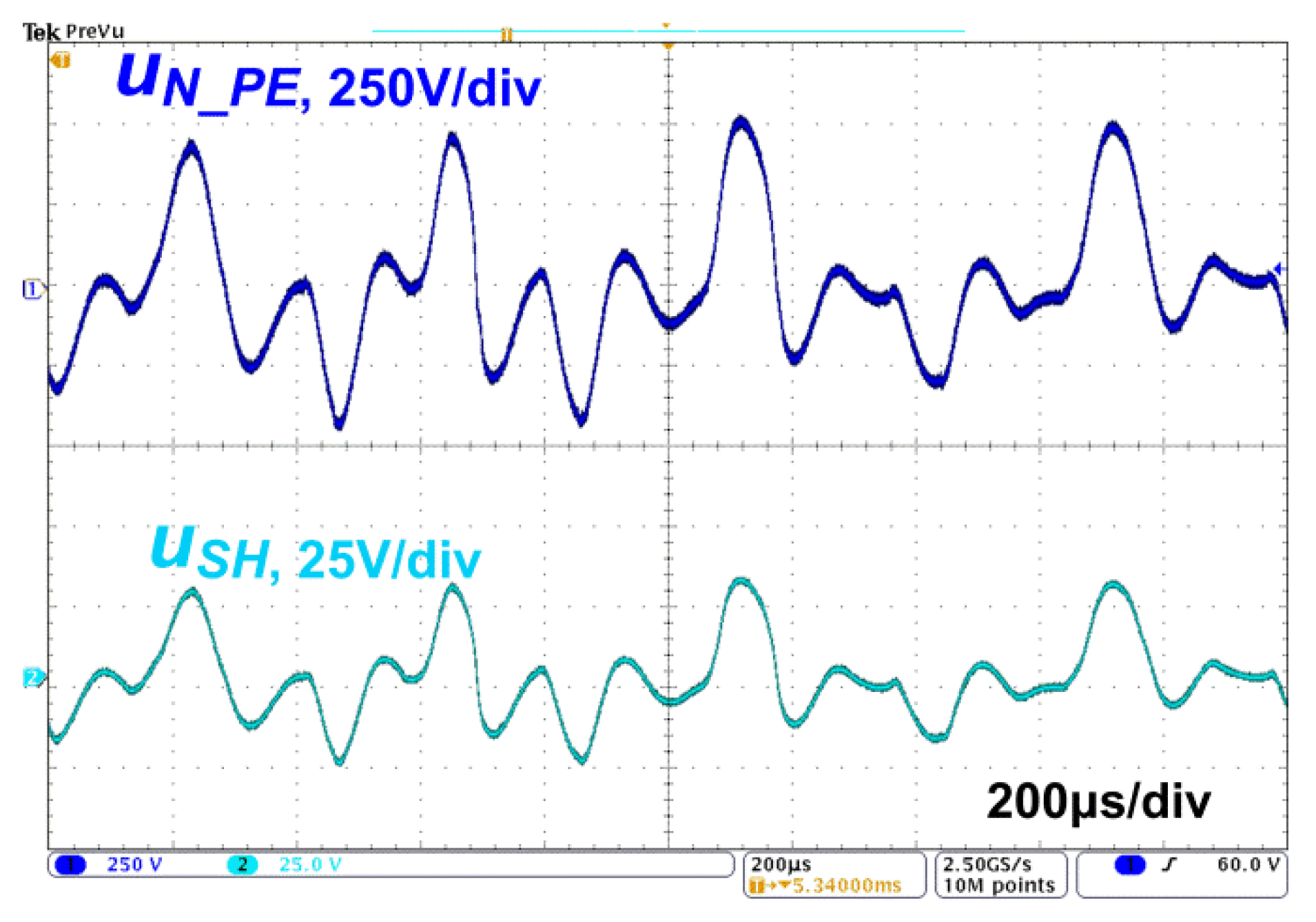
Considering the scheme presented in Figure 12b, it can be recognized that the CM choke inductance LC and parasitic capacitances of the wires and motor form a resonant circuit with a low attenuation rate. Hence, neglecting the impact of the motor windings’ impedance ZO and the cable parasitic components, if LC is high enough to meet the condition
f s w < 1 2 π 3 L C C P E ,
in uN_PE waveforms, undesirable oscillations may occur, in which maximum amplitudes significantly exceed UDC/2 (Figure 27). As a result, the uSH voltage maximum value is increased, and hence the possibility of EDM current occurrence rises.
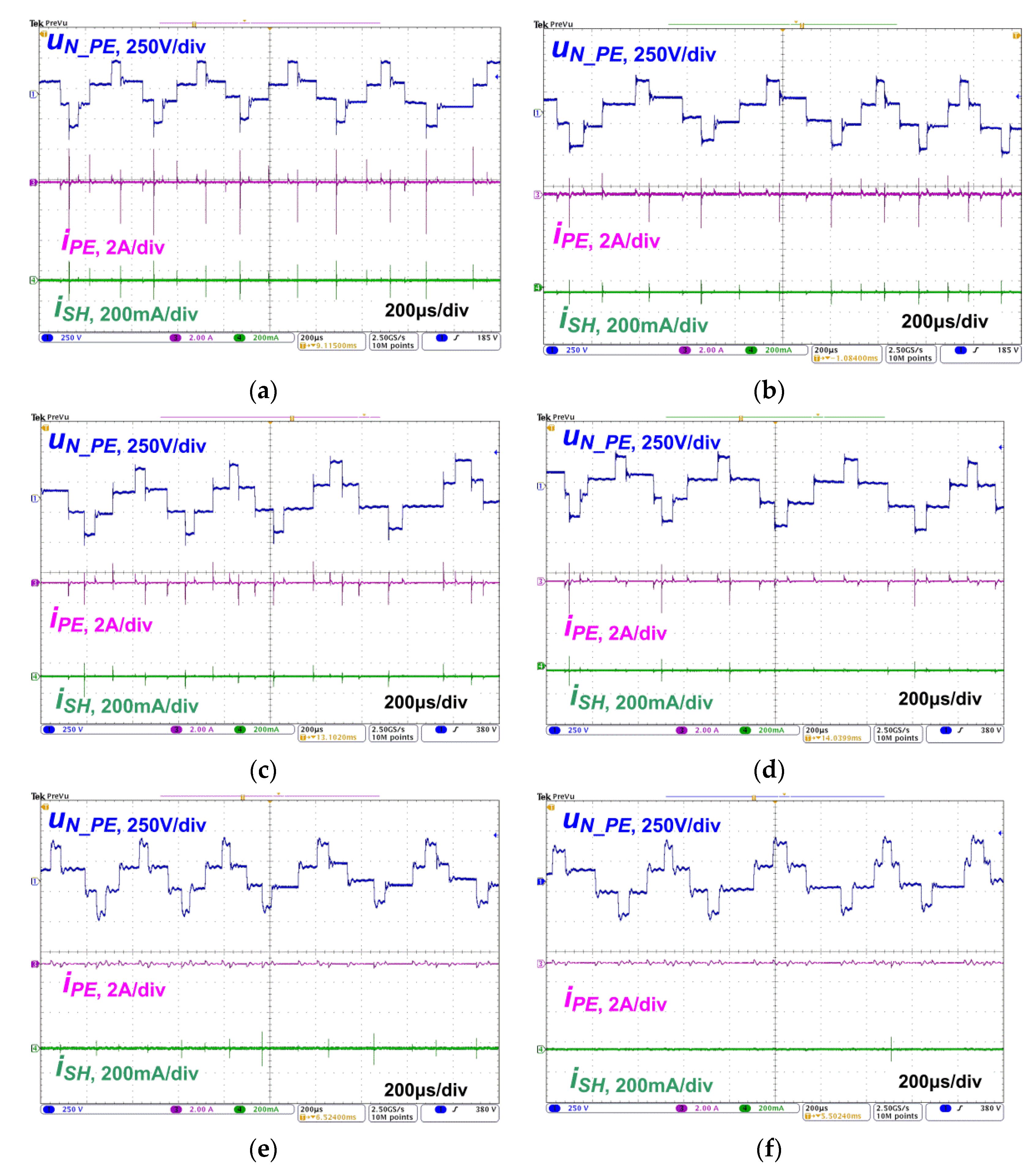
Comparative waveforms of the common-mode voltage uN_PE, ground leakage current iPE and motor shaft ground current iSH are depicted in Figure 28 and Figure 29. The observed overvoltage spikes of the uN_PE voltage are caused by the common-mode current flowing through motor inductances, which is excited during each inverter transistor’s switching. The maximum values of ground currents iPE and iSH are determined by the du/dt gradient of the uN_PE voltage, which results in currents’ capacitive character. It should be noted that the highest reduction in the duN_PE/dt gradient is noted in the drive configuration with the CM choke; hence, this solution demonstrates the highest effectiveness for a ground current reduction (Table 2). Similarly, a reduction in the iSH current maximum value due to a decrease in the duN_PE/dt gradient was also noted for all considered solutions.

5. Conclusions

In this paper, a survey of representative methods focused on the reduction in negative effects caused by a common-mode voltage influence was presented (Table 3). Basing on the results of the performed comparative tests, the highest effectiveness in the reduction in ground leakage currents and motor shaft-grounding currents was noticed for the drive configuration with a CM choke. The best improvement in motor supply conditions was noted when sine-wave filters were used. Applications of du/dt chokes and motor chokes brought moderate results. Hence, application of the configuration with a CM choke and a sine-wave filter may be proposed as the most reasonable solution [47]. However, it should be noted that the application of this configuration results in the highest power loss. For example, during the performed tests, at 1.5 kW of power measured at motor terminals, the obtained power loss equaled 2.7 W for the CM choke, 6.3 W for the du/dt choke and 53.7 W for the sine-wave filter in a configuration with a CM choke. It should also be noted that none of the tested typical commercial solutions ensure a reduction in common-mode voltage and motor shaft voltage levels; hence, they do not significantly improve the safety of motor bearings in terms of the possibility of EDM current occurrence.

Author Contributions

Conceptualization, M.T. and P.M.; methodology, M.T.; software, M.T.; validation, M.T.; formal analysis, P.M.; investigation, M.T.; resources, M.T.; data curation, M.T.; writing—original draft preparation, M.T. and P.M.; writing—review and editing, M.T. and P.M.; visualization, M.T. and P.M.; supervision, P.M.; project administration, M.T. and P.M.; funding acquisition, P.M. All authors have read and agreed to the published version of the manuscript.

Funding

This research received no external funding.

Institutional Review Board Statement

Not applicable.

Informed Consent Statement

Not applicable.

Data Availability Statement

Not applicable.

Conflicts of Interest

The authors declare no conflict of interest.

References

  1. Mohan, N. Electric Machines and Drives: A First Course; Wiley: Hoboken, NJ, USA, 2012. [Google Scholar]
  2. Koshti, A.K.; Rao, M.N. A brief review on multilevel inverter topologies. In Proceedings of the 2017 International Conference on Data Management, Analytics and Innovation (ICDMAI), Pune, India, 24–26 February 2017; pp. 187–193. [Google Scholar] [CrossRef]
  3. Han, D.; Morris, C.; Lee, W.; Sarlioglu, B. Determination of CM choke parameters for SiC MOSFET motor drive based on simple measurements and frequency domain modeling. In Proceedings of the 2016 IEEE Applied Power Electronics Conference and Exposition (APEC), Long Beach, CA, USA, 20–24 March 2016; pp. 2861–2867. [Google Scholar] [CrossRef]
  4. Shirabe, K. Efficiency Comparison between Si-IGBT-Based Drive and GaN-Based Drive. IEEE Trans. Ind. Appl. 2014, 50, 566–572. [Google Scholar] [CrossRef]
  5. Swamy, M.M.; Kang, J.-K.; Shirabe, K. Power Loss, System Efficiency, and Leakage Current Comparison between Si IGBT VFD and SiC FET VFD With Various Filtering Options. IEEE Trans. Ind. Appl. 2015, 51, 3858–3866. [Google Scholar] [CrossRef]
  6. Pastura, M.; Nuzzo, S.; Kohler, M.; Barater, D. Dv/Dt Filtering Techniques for Electric Drives: Review and Challenges. In Proceedings of the IECON 2019—45th Annual Conference of the IEEE Industrial Electronics Society, Lisbon, Portugal, 14–17 October 2019; pp. 7088–7093. [Google Scholar] [CrossRef] [Green Version]
  7. Acharya, B.A.; John, V. Design of output dv/dt filter for motor drives. In Proceedings of the 2010 5th International Conference on Industrial and Information Systems, Mangalore, India, 29 July–1 August 2010; pp. 562–567. [Google Scholar] [CrossRef]
  8. Guziński, J.; Abu-Rub, H.; Strankowski, P. Variable Speed AC Drives with Inverter Output Filters; John Wiley & Sons: Hoboken, NJ, USA, 2015. [Google Scholar]
  9. Finlayson, P.T. Output filters for PWM drives with induction motors. IEEE Ind. Appl. Mag. 1998, 4, 46–52. [Google Scholar] [CrossRef]
  10. Kerkman, R.; Leggate, D.; Skibinski, G. Interaction of drive modulation and cable parameters on AC motor transients. In Proceedings of the IAS ’96 Conference Record of the 1996 IEEE Industry Applications Conference Thirty-First IAS Annual Meeting, San Diego, CA, USA, 6–10 October 1996; Volume 1, pp. 143–152. [Google Scholar] [CrossRef]
  11. Hwang, D.-H.; Lee, K.-C.; Kim, Y.-J.; Bae, S.-W.; Kim, D.-H.; Ro, C.-G. Voltage stresses on stator windings of induction motors driven by IGBT PWM inverters. In Proceedings of the 38th IAS Annual Meeting on Conference Record of the Industry Applications Conference, 2003, Salt Lake City, UT, USA, 12–16 October 2003; Volume 1, pp. 439–444. [Google Scholar] [CrossRef]
  12. Fenger, M.; Campbell, S.R.; Pedersen, J. Dealing with motor winding problems caused by inverter drives. In Proceedings of the IEEE-IAS/PCS 2002 Cement Industry Technical Conference. Conference Record (Cat. No.02CH37282), Jacksonville, FL, USA, 5–9 May 2002; pp. 65–76. [Google Scholar] [CrossRef]
  13. Luszcz, J. High Frequency Conducted Emission in AC Motor Drives Fed by Frequency Converters: Sources and Propagation Paths; IEEE Press: Piscataway, NJ, USA; John Wiley & Sons: Hoboken, NJ, USA, 2018. [Google Scholar]
  14. Shen, W.; Wang, F.; Boroyevich, D.; Liu, Y. Definition and acquisition of CM and DM EMI noise for general-purpose adjustable speed motor drives. In Proceedings of the 2004 IEEE 35th Annual Power Electronics Specialists Conference (IEEE Cat. No.04CH37551), Aachen, Germany, 20–25 June 2004; pp. 1028–1033. [Google Scholar] [CrossRef]
  15. Qi, T.; Sun, J. DC bus grounding capacitance optimizatio for common-mode EMI minimization. In Proceedings of the 2011 Twenty-Sixth Annual IEEE Applied Power Electronics Conference and Exposition (APEC), Fort Worth, TX, USA, 6–11 March 2011; pp. 661–666. [Google Scholar] [CrossRef]
  16. Pairodamonchai, P.; Sangwongwanich, S. Exact common-mode and differential-mode equivalent circuits of inverters in motor drive systems taking into account input rectifiers. In Proceedings of the 2011 IEEE Ninth International Conference on Power Electronics and Drive Systems, Singapore, 5–8 December 2011; pp. 278–285. [Google Scholar] [CrossRef]
  17. Fan, F.; See, K.Y.; Liu, X.; Li, K.; Gupta, A.K. Systematic Common-Mode Filter Design for Inverter-Driven Motor System Based on In-Circuit Impedance Extraction. IEEE Trans. Electromagn. Compat. 2020, 62, 1711–1722. [Google Scholar] [CrossRef]
  18. Adabi, J.; Zare, F.; Ledwich, G.; Ghosh, A. Leakage current and common mode voltage issues in modern AC drive systems. In Proceedings of the 2007 Australasian Universities Power Engineering Conference, Perth, Australia, 9–12 December 2007; pp. 1–6. [Google Scholar] [CrossRef] [Green Version]
  19. Chen, S.; Lipo, T.A.; Novotny, D.W. Circulating type motor bearing current in inverter drives. In Proceedings of the 1996 IEEE Industry Applications Society Annual Meeting (IAS), San Diego, CA, USA, 6–10 October 1996; Volume 1, pp. 162–167. [Google Scholar] [CrossRef]
  20. Turzynski, M.; Chrzan, P.J. Reducing Common-Mode Voltage and Bearing Currents in Quasi-Resonant DC-Link Inverter. IEEE Trans. Power Electron. 2020, 35, 9553–9562. [Google Scholar] [CrossRef]
  21. Mechlinski, M.; Schroder, S.; Shen, J.; De Doncker, R.W. Grounding Concept and Common-Mode Filter Design Methodology for Transformerless MV Drives to Prevent Bearing Current Issues. IEEE Trans. Ind. Appl. 2017, 53, 5393–5404. [Google Scholar] [CrossRef]
  22. Plazenet, T.; Boileau, T.; Caironi, C.; Nahid-Mobarakeh, B. A Comprehensive Study on Shaft Voltages and Bearing Currents in Rotating Machines. IEEE Trans. Ind. Appl. 2018, 54, 3749–3759. [Google Scholar] [CrossRef]
  23. Muetze, A.; Binder, A. Don’t lose your bearings. IEEE Ind. Appl. Mag. 2006, 12, 22–31. [Google Scholar] [CrossRef]
  24. Plazenet, T.; Boileau, T.; Caironi, C.; Nahid-Mobarakeh, B. An overview of shaft voltages and bearing currents in rotating machines. In Proceedings of the 2016 IEEE Industry Applications Society Annual Meeting, Portland, OR, USA, 2–6 October 2016; pp. 1–8. [Google Scholar] [CrossRef]
  25. Busse, D.; Erdman, J.; Kerkman, R.J.; Schlegel, D.; Skibinski, G. Bearing currents and their relationship to PWM drives. IEEE Trans. Power Electron. 1997, 12, 243–252. [Google Scholar] [CrossRef] [Green Version]
  26. Joshi, A.; Blennow, J. Electrical characterization of bearing lubricants. In Proceedings of the 2014 IEEE Conference on Electrical Insulation and Dielectric Phenomena (CEIDP), Des Moines, IA, USA, 19–22 October 2014; pp. 586–589. [Google Scholar] [CrossRef]
  27. Akagi, H.; Tamura, S. A Passive EMI Filter for Eliminating Both Bearing Current and Ground Leakage Current From an Inverter-Driven Motor. IEEE Trans. Power Electron. 2006, 21, 1459–1469. [Google Scholar] [CrossRef]
  28. Chen, S.; Lipo, T.A.; Fitzgerald, D. Source of induction motor bearing currents caused by PWM inverters. IEEE Trans. Energy Convers. 1996, 11, 25–32. [Google Scholar] [CrossRef]
  29. Bearing Currents in Modern AC Drive Systems. ABB Technical Guide. Available online: https://library.e.abb.com (accessed on 1 June 2021).
  30. Lai, Y.-S.; Chen, P.-S.; Lee, H.-K.; Chou, J. Optimal Common-Mode Voltage Reduction PWM Technique for Inverter Control With Consideration of the Dead-Time Effects—Part II: Applications to IM Drives With Diode Front End. IEEE Trans. Ind. Appl. 2004, 40, 1613–1620. [Google Scholar] [CrossRef]
  31. Kimball, J.W.; Zawodniok, M. Reducing Common-Mode Voltage in Three-Phase Sine-Triangle PWM with Interleaved Carriers. IEEE Trans. Power Electron. 2011, 26, 2229–2236. [Google Scholar] [CrossRef]
  32. Alcaide, A.M.; Yan, H.; Wang, X.; León Galván, J.I.; Portillo Guisado, R.C.; Buticchi, G.; Vazquez, S.; Monopoli, V.G.; Liserre, M.; García Franquelo, L. Common-Mode Voltage Mitigation Technique in Motor Drive Applications by Applying a Sampling-Time Adaptive Multi-Carrier PWM Method. IEEE Access 2021, 9, 56115–56126. [Google Scholar] [CrossRef]
  33. Park, C.-H.; Seo, I.-K.; Negesse, B.B.; Yoon, J.; Kim, J.-M. A Study on Common Mode Voltage Reduction Strategies According to Modulation Methods in Modular Multilevel Converter. Energies 2021, 14, 1607. [Google Scholar] [CrossRef]
  34. Ogasawara, S.; Ayano, H.; Akagi, H. An active circuit for cancellation of common-mode voltage generated by a PWM inverter. In Proceedings of the 1997 28th Annual IEEE Power Electronics Specialists Conference (PESC), St. Louis, MO, USA, 22–27 June 1997; Volume 2, pp. 1547–1553. [Google Scholar] [CrossRef] [Green Version]
  35. Bhakthavachala, A.; Anuradha, K. A Simplified Filter Topology for Compensating Common Mode Voltage and Electromagnetic Interference in Induction Motor Drives. Energy Procedia 2017, 117, 377–384. [Google Scholar] [CrossRef]
  36. Takahashi, S.; Ogasawara, S.; Takemoto, M.; Orikawa, K.; Tamate, M. Common-Mode Voltage Attenuation of an Active Common-Mode Filter in a Motor Drive System Fed by a PWM Inverter. IEEE Trans. Ind. Appl. 2019, 55, 2721–2730. [Google Scholar] [CrossRef]
  37. Lin, Z.; Lei, B.; Wu, L.; Mei, P. Eliminating the Effect of Common-Mode Voltage on an Open-End Winding PMSM Based on Model Predictive Torque Control. Math. Probl. Eng. 2021, 2021, 1–11. [Google Scholar] [CrossRef]
  38. Von Jauanne, A.; Zhang, H. A dual-bridge inverter approach to eliminating common-mode voltages and bearing and leakage currents. IEEE Trans. Power Electron. 1999, 14, 43–48. [Google Scholar] [CrossRef]
  39. Baranwal, R.; Basu, K.; Mohan, N. Carrier-Based Implementation of SVPWM for Dual Two-Level VSI and Dual Matrix Converter With Zero Common-Mode Voltage. IEEE Trans. Power Electron. 2015, 30, 1471–1487. [Google Scholar] [CrossRef]
  40. Divan, D.M. The resonant DC link converter-a new concept in static power conversion. IEEE Trans. Ind. Appl. 1989, 25, 317–325. [Google Scholar] [CrossRef]
  41. Turzyński, M.; Chrzan, P.J. Resonant DC link inverters for AC motor drive systems–critical evaluation. Bull. Pol. Acad. Sci. Tech. Sci. 2019, 67, 241–252. [Google Scholar] [CrossRef]
  42. Li, R.; Xu, D. A Zero-Voltage Switching Three-Phase Inverter. IEEE Trans. Power Electron. 2014, 29, 1200–1210. [Google Scholar] [CrossRef]
  43. Kedarisetti, J.; Mutschler, P. A Motor-Friendly Quasi-Resonant DC-Link Inverter with Lossless Variable Zero-Voltage Duration. IEEE Trans. Power Electron. 2012, 27, 2613–2622. [Google Scholar] [CrossRef]
  44. Turzyński, M.; Frivaldsky, M. Modeling of a Quasi-Resonant DC Link Inverter Dedicated to Common-Mode Voltage and Ground Current Reduction. Energies 2020, 13, 5090. [Google Scholar] [CrossRef]
  45. Sojka, P.; Pipiska, M.; Frivaldsky, M. GaN power transistor switching performance in hard-switching and soft-switching modes. In Proceedings of the 2019 20th International Scientific Conference on Electric Power Engineering (EPE), Kouty nad Desnou, Czech Republic, 15–17 May 2019; pp. 1–5. [Google Scholar] [CrossRef]
  46. Huang, J.; Shi, H. A Hybrid Filter for the Suppression of Common-Mode Voltage and Differential-Mode Harmonics in Three-Phase Inverters with CPPM. IEEE Trans. Ind. Electron. 2015, 62, 3991–4000. [Google Scholar] [CrossRef]
  47. Baek, S.; Choi, D.; Bu, H.; Cho, Y. Analysis and Design of a Sine Wave Filter for GaN-Based Low-Voltage Variable Frequency Drives. Electronics 2020, 9, 345. [Google Scholar] [CrossRef] [Green Version]
  48. Luu, T.; Shudarek, T. An integrated inverter output passive sinewave filter for eliminating both common and differential mode PWM motor drive problems. In Proceedings of the 2017 IEEE Applied Power Electronics Conference and Exposition (APEC), Tampa, FL, USA, 26–30 March 2017; pp. 373–379. [Google Scholar] [CrossRef]
  49. Muller, J.-K.; Manthey, T.; Han, D.; Sarlioglu, B.; Friebe, J.; Mertens, A. Output Sine-Wave Filter Design and Characterization for a 10 kW SiC Inverter. In Proceedings of the 2019 IEEE Energy Conversion Congress and Exposition (ECCE), Baltimore, MD, USA, 29 September–3 October 2019; pp. 359–366. [Google Scholar] [CrossRef]
  50. Guzinski, J.; Abu-Rub, H. Sensorless induction motor drive with voltage inverter and sine-wave filter. In Proceedings of the 2013 IEEE International Symposium on Sensorless Control for Electrical Drives and Predictive Control of Electrical Drives and Power Electronics (SLED/PRECEDE), München, Germany, 17–19 October 2013; pp. 1–8. [Google Scholar] [CrossRef]
  51. Chysky, J.; Novak, J.; Novak, M. Losses in sinusoidal filter chokes. In Proceedings of the IECON 2013—39th Annual Conference of the IEEE Industrial Electronics Society, Vienna, Austria, 10–13 November 2013; pp. 7790–7794. [Google Scholar] [CrossRef]
  52. Habetler, T.G.; Naik, R.; Nondahl, T.A. Design and implementation of an inverter output LC filter used for dv/dt reduction. IEEE Trans. Power Electron. 2002, 17, 327–331. [Google Scholar] [CrossRef]
  53. Palma, L.; Enjeti, P. An inverter output filter to mitigate dV/dt effects in PWM drive system. In Proceedings of the APEC. Seventeenth Annual IEEE Applied Power Electronics Conference and Exposition (Cat. No.02CH37335), Dallas, TX, USA, 10–14 March 2002; pp. 550–556. [Google Scholar] [CrossRef]
  54. Heldwein, M.L.; Dalessandro, L.; Kolar, J.W. The Three-Phase Common-Mode Inductor: Modeling and Design Issues. IEEE Trans. Ind. Electron. 2011, 58, 3264–3274. [Google Scholar] [CrossRef]
  55. Muetze, A.; Sullivan, C.R. Simplified Design of Common-Mode Chokes for Reduction of Motor Ground Currents in Inverter Drives. IEEE Trans. Ind. Appl. 2011, 47, 2570–2577. [Google Scholar] [CrossRef]
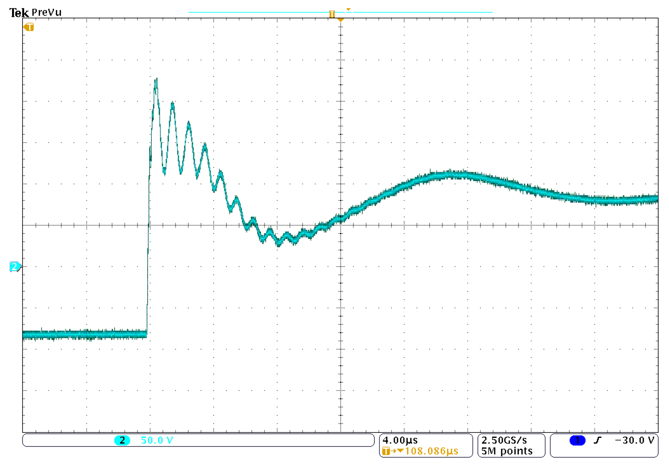
Figure 1. A phase voltage measured on the motor terminals (motor was connected to the inverter through a cable of 2.5 m in length).
Energies 14 04003 g001
Figure 2. Common-mode currents’ propagation paths in electric drive fed by the voltage inverter (ground capacitances of transistors TF1 and TF6 are marked).
Energies 14 04003 g002
Figure 3. Electric drive fed by a conventional hard-switched two-level bridge voltage inverter.
Energies 14 04003 g003
Figure 4. Bearing cross-section: (a) hybrid; (b) insulated.
Energies 14 04003 g004
Figure 5. Principle of inverter output voltage forming: (a) classic space vector pulse width modulation (SVPWM); (b) active zero voltage control modulation.
Energies 14 04003 g005
Figure 6. Active common noise canceller.
Energies 14 04003 g006
Figure 7. Dual two-level inverter.
Energies 14 04003 g007
Figure 8. Concept of the parallel quasi-resonant DC link inverter (PQRDCLI) with two insulating switches T1,D1 and T2,D2: (a) scheme; (b) uF zero voltage notches.
Energies 14 04003 g008
Figure 9. Electric drive with motor choke.
Energies 14 04003 g009
Figure 10. Electric drive with a sine-wave filter.
Energies 14 04003 g010
Figure 11. Electric drive with an exemplary du/dt filter presented in [52].
Energies 14 04003 g011
Figure 12. Electric drive with a CM choke: (a) application scheme, (b) equivalent circuit for common-mode components, (c) CM choke realization, (d) view of commercial CM choke type BE1871/720 μH (TTI).
Energies 14 04003 g012
Figure 13. A common-mode impedance ZC measurement setup.
Energies 14 04003 g013
Figure 14. Measured impedance ZC(f) frequency characteristics: (a) motor; (b) motor with 1 m cable; (c) motor with 10 m cable.
Energies 14 04003 g014
Figure 15. Measured impedance ZC(f) frequency characteristics: (a) motor + du/dt choke (LDT = 0.31 mH) + 1 m cable; (b) motor + du/dt choke (LDT = 0.31 mH) + 10 m cable.
Energies 14 04003 g015
Figure 16. Measured impedance ZC(f) frequency characteristics: (a) motor + motor choke (LD = 3.8 mH) + 1 m cable; (b) motor + motor choke (LD = 3.8 mH) + 10 m cable.
Energies 14 04003 g016
Figure 17. Measured impedance ZC(f) frequency characteristics: (a) motor + sine-wave filter (LS = 3.8 mH, CS = 15 uF) + 1 m cable; (b) motor + sine-wave filter (LS = 3.8 mH, CS = 15 uF) + 10 m cable.
Energies 14 04003 g017
Figure 18. Measured impedance ZC(f) frequency characteristics: (a) motor + CM choke (LC = 0.72 mH) + 1 m cable; (b) motor + CM choke (LC = 0.72 mH) + 10 m cable.
Energies 14 04003 g018
Figure 19. Laboratory setup for experimental tests: (a) scheme; (b) a photo of an experimental setup in a configuration with a motor choke.
Energies 14 04003 g019
Figure 20. Experimental waveforms of voltage uC_PE recorded in a configuration with a single inverter and in the configuration of an inverter with a 0.31 mH du/dt choke (10 m cable).
Energies 14 04003 g020
Figure 21. Spectrum of voltage uC_PE recorded in a configuration with: (a,c,e,g,i) 1 m cable; (b,d,f,h,j) 10 m cable.
Energies 14 04003 g021
Figure 22. Experimental waveforms of line-to-line voltage uAB and current iA measured at motor terminals in a configuration with a 1 m cable for: (a) inverter; (b) motor choke; (c) du/dt choke; (d) sine-wave filter; (e) CM choke; (f) CM choke with sine-wave filter.
Energies 14 04003 g022
Figure 23. Experimental waveforms of line-to-line voltage uAB and current iA measured at motor terminals in a configuration with a 10 m cable for: (a) inverter; (b) motor choke; (c) du/dt choke; (d) sine-wave filter; (e) CM choke; (f) CM choke with sine-wave filter.
Energies 14 04003 g023
Figure 24. Experimental waveforms of CM voltage uN_PE and motor shaft voltage uSH measured in a configuration with a 1 m cable for: (a) inverter; (b) motor choke; (c) du/dt choke; (d) sine-wave filter; (e) CM choke; (f) CM choke with sine-wave filter.
Energies 14 04003 g024
Figure 25. Experimental waveforms of CM voltage uN_PE and motor shaft voltage uSH measured in a configuration with a 10 m cable for: (a) inverter; (b) motor choke; (c) du/dt choke; (d) sine-wave filter; (e) CM choke; (f) CM choke with sine-wave filter.
Energies 14 04003 g025
Figure 26. Electric drive fed by a conventional hard-switched two-level bridge voltage inverter in a configuration with a sine-wave filter.
Energies 14 04003 g026
Figure 27. Experimental waveforms of the common-mode voltage uN_PE and motor shaft voltage uSH of a motor fed by the AC10 10G-44-0170-BF (Parker) inverter in a configuration with a CM choke with increased inductance LC (LC = 28 mH).
Energies 14 04003 g027
Figure 28. Experimental waveforms of CM voltage uN_PE, leakage current iPE and shaft-grounding brush current iSH measured in a configuration with a 1 m cable for: (a) inverter; (b) motor choke; (c) du/dt choke; (d) sine-wave filter; (e) CM choke; (f) CM choke with sine-wave filter.
Energies 14 04003 g028
Figure 29. Experimental waveforms of CM voltage uN_PE, leakage current iPE and shaft-grounding brush current iSH measured in a configuration with a 10 m cable for: (a) inverter; (b) motor choke; (c) du/dt choke; (d) sine-wave filter; (e) CM choke; (f) CM choke with sine-wave filter.
Energies 14 04003 g029
Table 1. Effectiveness of the most commonly applied solutions dedicated to bearing current reduction.
Bearing Current TypeEDM CurrentsCirculating CurrentsRotor Ground Currents
Solution
shielded cablesno influencepossible increase at higher rotor shaft speedpartial reduction
grounding of one end of rotor shaft via brushcomplete reductioneffective, if an opposite bearing is made as hybrid bearing or insulated onepossible increase if a non-insulated clutch is applied between motor and load
insulated bearingspartial reductionpartial reductionpartial reduction
hybrid bearingscomplete reductioncomplete reductioncomplete reduction
Table 2. Common-mode impedance model parameters of a 7.5 kW motor with hybrid bearings 6308-2RS (ZCS Ceramit).
Configuration|duA_PE/dt| (kv/μs)UAB(max)/UDC (–)IPE(max) (A)ISH(max) (mA)|uN_PE/UDC| (–)
cable length:1 m10 m1 m10 m1 m10 m1 m10 m1 m10 m
inverter7.085.571.452.053.753.371581461/21/2
inverter + motor choke (LD = 3.8 mH)2.622.421.441.472.232.08132601/21/2
inverter + du/dt choke (LDT = 0.31 mH)1.271.041.431.461.451.7370861/21/2
inverter + sine-wave filter (LS = 3.8 mH, CS = 15 µF)1.571.331.121.161.911.73105951/21/2
inverter + CM choke (LC = 0.72 mH)1.091.282.102.160.280.825112981/21/2
inverter + sine-wave filter + CM choke (LS = 0.31 mH, CS = 15 µF, LC = 0.72 mH)0.120.091.121.130.250.4380401/21/2
Table 3. Main features of compared reduction methods of common-mode voltage impact in electric drives.
TechniqueCM Voltage LevelsGround Leakage Current SuppressionUsage
Requirements
AdvantagesDisadvantages
Modification of modulation strategy [8,30,31,32]±UDC/6 [32]reported 50% [32]required modification of inverter modulation strategy and control algorithms
-
suppression of ground leakage current
-
significant reduction in uN_PE voltage levels
-
low cost
-
increase in THD of motor current
-
undesirable spikes, whose amplitude exceeds ±UDC/2, may be noted in CM voltage waveforms when AZVC technique is applied
-
cannot be used with commercial inverters, whose control system’s access is made unavailable for users with further modifications
Active common noise canceller [34,35,36]reported reduction in uN_PE voltage levels more than 90% regardless of the inverter transistors’ state [36]reported up to 90% [34]implemented between motor and inverter, access to both DC link buses between rectifier and inverter is required
-
high reduction in uN_PE voltage levels
-
high suppression of ground leakage current
-
high cost
-
a high-frequency, four-winding transformer is required
-
high complexity
-
requires access to both DC link buses between rectifier and inverter
Dual two-level inverter [37,38,39]±UDC/3 [39]reported up to 50% [38]required use of dual inverter and motor with open stator windings
-
suppression of ground leakage current
-
reduction in uN_PE voltage levels
-
high complexity of control system and control algorithms
-
high cost
PQRDCLI with two insulating switches [20,43]±UDC/6 [20]reported up to 80% [20]required modifications of inverter DC link circuit, control systems and control algorithms
-
high suppression of ground leakage current
-
significant reduction in uN_PE voltage levels
-
decrease in generated conducted disturbances, especially in a range of frequency from 0.6 to 15 MHz
-
possibility of implementation of control methods based on SVPWM modulators
-
high complexity
-
high cost
-
in comparison with hard-switched inverters, energy efficiency of PQRDCLI is lower at low loads
motor choke±UDC/2moderate reduction (about 40%)applied between motor and inverter, no additional modifications of inverter topology or control algorithms are needed
-
simplicity
-
moderate cost
-
enables a smoothing of motor current and reducing du/dt voltage gradients at the motor terminals
-
reduction in overvoltage at motor terminals
-
no reduction in CM voltage levels
-
large dimensions
-
generation of additional voltage drop and power loss
du/dt choke±UDC/2moderate reduction (about 50%)applied between motor and inverter, no additional modifications of inverter topology or control algorithms are needed
-
simplicity
-
moderate cost
-
reduction in du/dt voltage gradients affecting the motor
-
reduction in overvoltage at motor terminals
-
lower dimensions than motor chokes
-
no reduction in CM voltage levels
-
dimensions
-
additional power loss and voltage drop
sine-wave filter±UDC/2moderate reduction (about 50%)applied between motor and inverter, no additional modifications of inverter topology are needed
-
simplicity
-
significant improvement in motor supply conditions (near sinusoidal profile of motor currents and voltage waveforms)
-
no reduction in CM voltage levels
-
large dimensions
-
generation of high power loss
-
high cost
-
sometimes modification of motor control algorithm is required
CM choke±UDC/2high reduction (about 80%)applied between motor and inverter, no additional modifications of inverter topology or control algorithms are needed
-
simplicity
-
low cost
-
low power loss
-
small dimensions
-
significant reduction in ground leakage current
-
no reduction in CM voltage levels
-
no reduction in differential-mode disturbances
-
no improvement in motor supply conditions
-
complicated design process
-
if CM choke impedance is too much, undesirable oscillations may occur in uN_PE waveforms, in which maximum amplitudes significantly exceed UDC/2
CM choke + sine-wave filter±UDC/2highest reduction (about 90%)applied between motor and inverter, no additional modifications of inverter topology are needed
-
simplicity
-
the highest reduction in ground leakage current
-
significant improvement in motor supply conditions
combines disadvantages of sine-wave filters and CM chokes
Publisher’s Note: MDPI stays neutral with regard to jurisdictional claims in published maps and institutional affiliations.