1. Introduction
With the rapid development of the Internet of things (IoT), high-performance power management integrated circuits are in great demand. Since small size, low cost, and long service time are desired for consumer electronics, the properties of DC–DC switching converters should meet the requirements such as minimal number of external components, high conversion efficiency, and small chip area of their control circuits. The peak current mode control is widely used in DC–DC converters due to the advantages of constant switching frequency, input voltage feedforward property, and automatic over-current protection [
1]. However, frequency compensation is needed for the peak current mode control to ensure the stability of the DC–DC converter. Not only are compensation components needed but the transient response of the DC–DC converter is also restricted. In recent years, a ripple-based constant on-time (RBCOT) control scheme for buck converters, as shown in
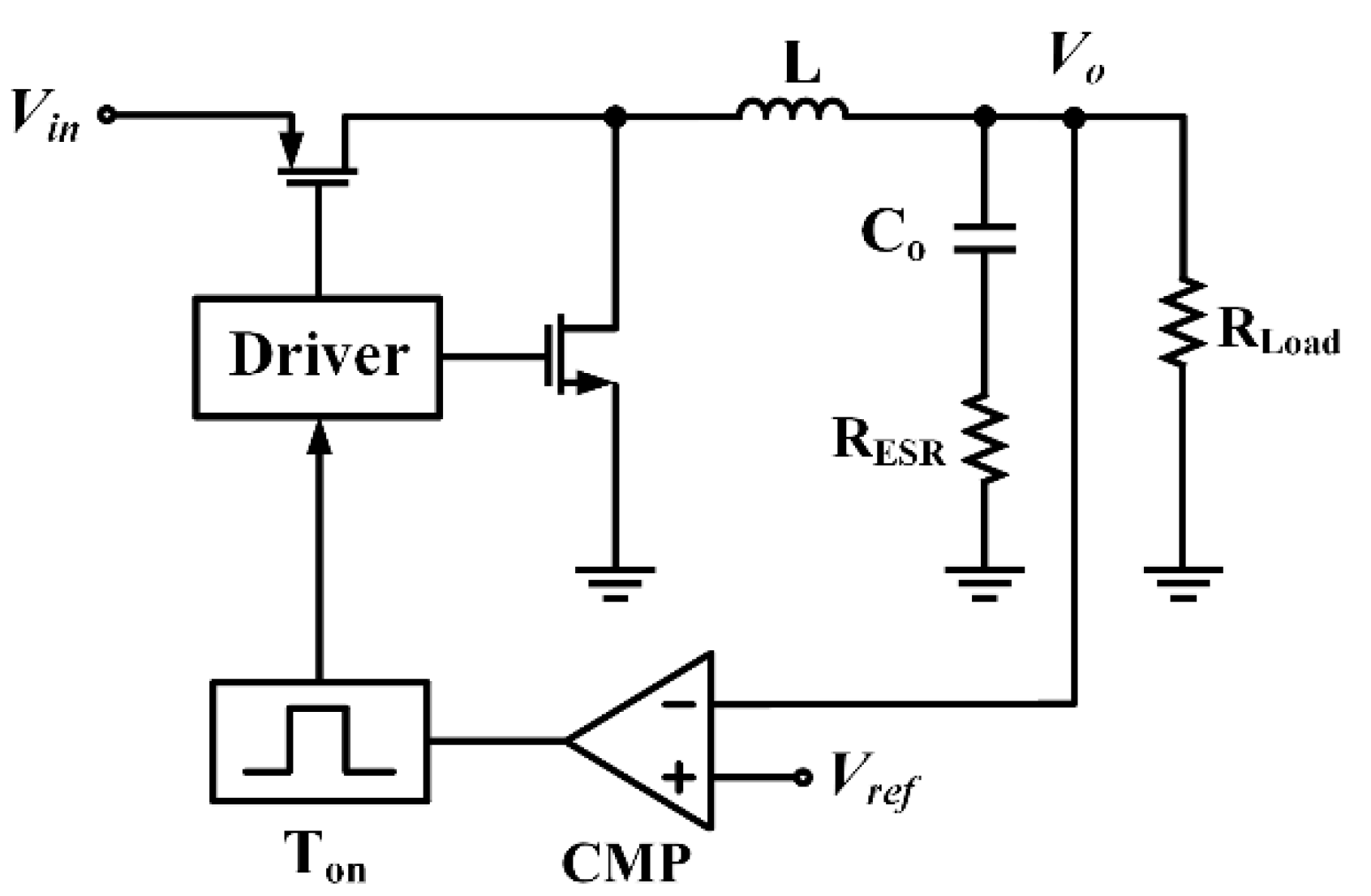
Figure 1, has received wide attention because of its simple structure, good light-load efficiency, and fast load transient response [
2,
3,
4,
5,
6,
7].
Due to low cost, small size, long lifetime, small variation of quality at different frequencies, and high temperature limit, the multilayer ceramic capacitor (MLCC) is widely used in buck converters. However, the RBCOT control requires an output capacitor with large equivalent-series resistance (ESR) to meet stability criteria, whereby the product of the output capacitance and its ESR should be larger than half of the on-time period [
8,
9,
10]. Thus, the low ESR of an MLCC would cause instability of the RBCOT buck converter. Due to valley voltage operation, the RBCOT buck converter suffers from the DC offset issue on the regulated output voltage [
11,
12]. The output DC offset is proportional to the output voltage ripple.
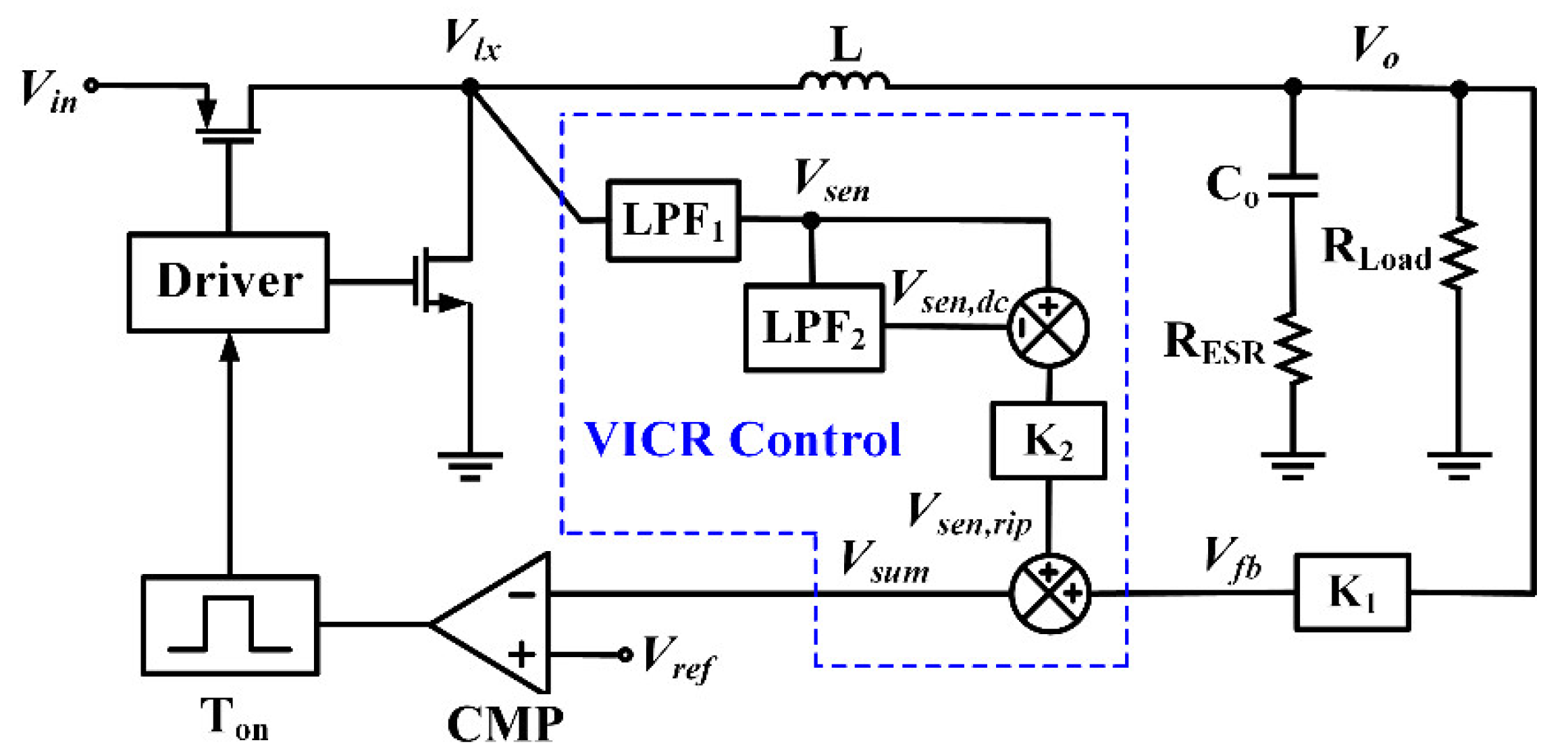
To alleviate the instability issue with low ESR of a capacitor, a virtual inductor current ripple (VICR) control method was presented [
8,
9,
10,
11,
12,
13,
14,
15,
16]. Since the VICR control adds an additional signal of inductor current ripple into the output feedback path, the stability constraint on large ESR can be relaxed. However, the VICR control enlarges output DC offset due to the additional signal. To fulfill the VICR control, two low-pass filters are needed, as shown in the part B of
Section 2 in [
8]. The low-pass filters occupy a significant chip area; hence, this method may be inappropriate for integrated circuit design. To reduce the output DC offset issue caused by the VICR control, the pseudowave tracking method is presented [
9]. The valley detector is used to sense the valley voltage of the sensed inductor current. Then, through the dual differential amplifier, the output feedback signal becomes the valley voltage of the summation signal. Thus, the output DC offset issue is removed. Nevertheless, an inductor current sensor, a trimming mechanism, and an LPF in valley detector are needed; thus, the design difficulty and silicon area are increased. A current-mode on-time controlled buck converter is presented to solve the low ESR issue [
15,
16]. However, an error amplifier and off-chip compensation components are required, thereby increasing the size and cost of the converter.
Due to ripple-based control scheme, the RBCOT buck converter is a clock-free architecture. Its switching frequency varies when the input voltage, output voltage, and load current are changed [
15,
17,
18]. This improves the power efficiency of the RBCOT converter at light load, but this control is prone to electromagnetic interference (EMI) issues. Analog circuits such as radiofrequency circuits, digital-to-analog converters, analog-to-digital converters, and audio systems are sensitive to switching frequency interference because frequency variation can degrade their performance. Therefore, switching frequency variation of the RBCOT buck converter is required to be constrained to enhance the system performance. Several previous studies proposed techniques to alleviate the variation of switching frequency. Although a phase-locked loop can be employed in the COT control to lock switching frequency at a predefined value [
2,
19,
20], additional complicated circuits and components are required to increases silicon area and cost. References [
15,
21] used the information of input voltage and output voltage to adjust on-time period to maintain constant switching frequency. However, switching frequency still varied with different load currents. Moreover, a previous study adopted the output signal of its error amplifier to keep constant switching frequency [
16]. Nevertheless, the relationship among the on resistance of the high-side power transistor, direct current resistance (DCR) of the inductor, and two resistances used in a current sensor should be constrained [
16]; therefore, the design difficulty is increased. Another method applied a current sensor and load current corrector to revise the on-time period [
12], but the reduction in switching frequency variation was insignificant.
This paper proposes a wave tracking reference (WTR) control for the low ESR of an MLCC to improve system stability and concurrently eliminate output DC offset. Since the circuit of the WTR control is implemented in an integrated circuit (IC) without any low-pass filter, trimming mechanism, or off-chip component, the chip area can be reduced with no additional IC pin. Furthermore, an adaptive on-time (AOT) circuit is presented to minimize the switching frequency variation of buck converter in case of load current changes. The design of the proposed AOT circuit is simple and results in low power consumption. Hence, by employing the VICR control and AOT circuit, the chip area and EMI issue can be reduced significantly while the output regulation accuracy is improved. The remainder of this paper is organized as follows.
Section 2 discusses the output DC offset and frequency variation analysis in the RBCOT buck converter. The proposed AOT buck converter with WTR control and the implementation of crucial control circuits are illustrated in
Section 3.
Section 4 shows the experimental results. Lastly, a conclusion is given in
Section 5.
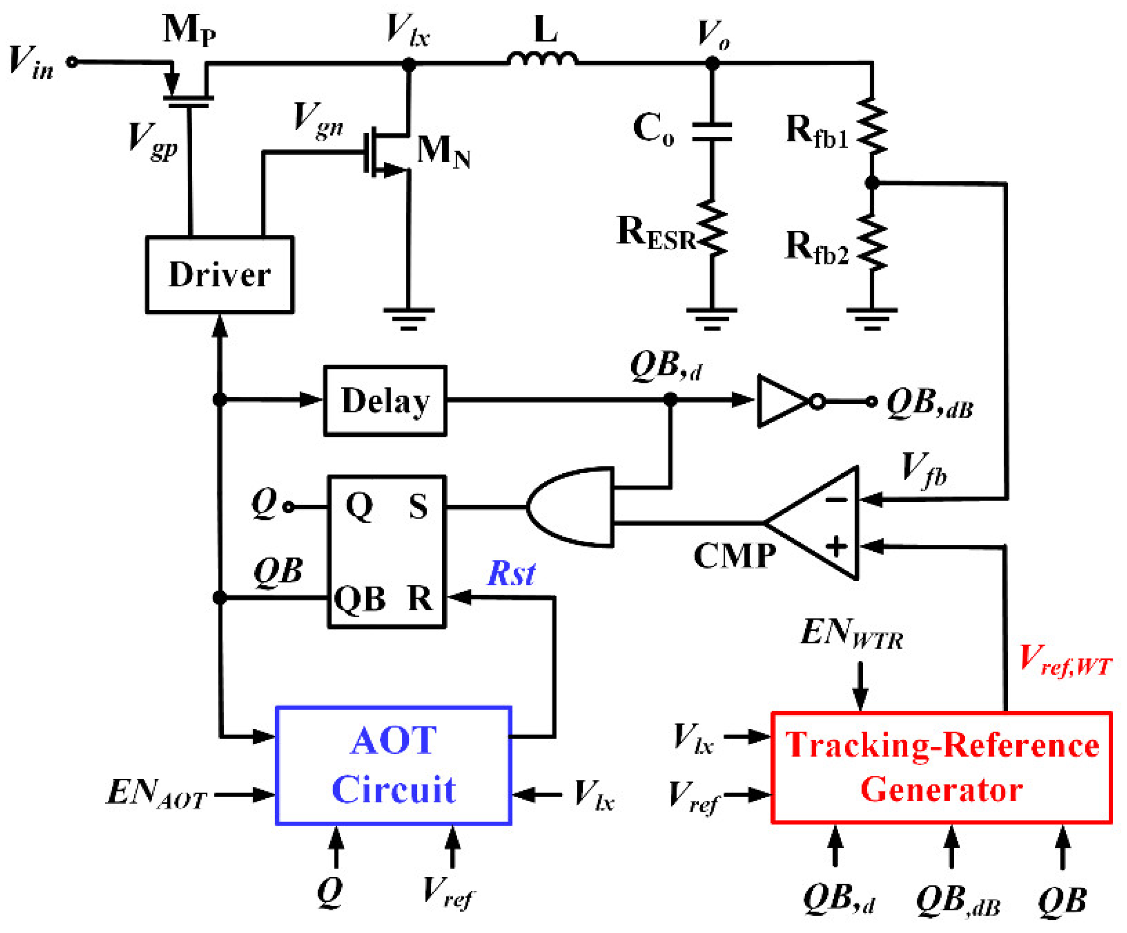
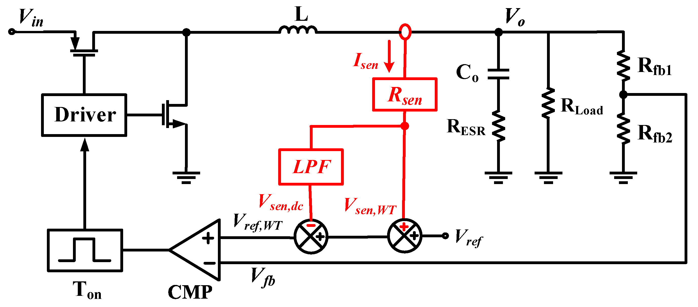
3. Adaptive On-Time Buck Converter with the Wave Tracking Reference Control
The block diagram of adaptive on-time (AOT) buck converter with the wave tracking reference (WTR) control is illustrated in
Figure 4. To solve the aforementioned issue, the WTR control is proposed to improve converter stability and concurrently eliminate output DC offset. Therefore, the low ESR of an MLCC can be used, and small output voltage ripple in a steady state is achieved in this work. The AOT circuit is employed to suppress the switching frequency variation of the buck converter operating in CCM in case of load current changes.
The scale-down output feedback signal Vfb is compared with the WTR signal Vref,WT produced by the tracking reference generator. When Vfb is smaller than Vref,WT, the comparator output exists in a high state. At this instant, signal QB,d is in a high state, and terminal S of the SR latch also exists in a high state. Subsequently, power transistors MP and MN are turned on and off, respectively, and the on-time period of MP is determined by the AOT circuit. The gate driver with dead time function is applied to provide sufficient driving capability and prevent shoot-through current. During the on-time period, the inductor current increases. At the end of the on-time period, signal Rst is set to a high state, and then the input voltage Vin stops charging the output inductor. When Vfb is lower than Vref,WT, MP is turned on again.
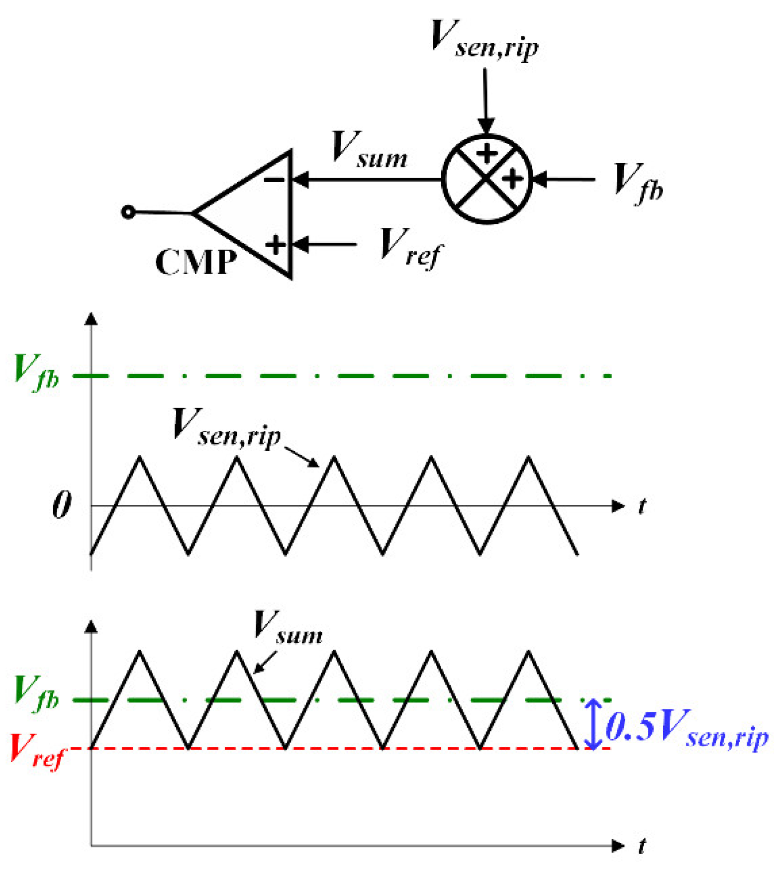
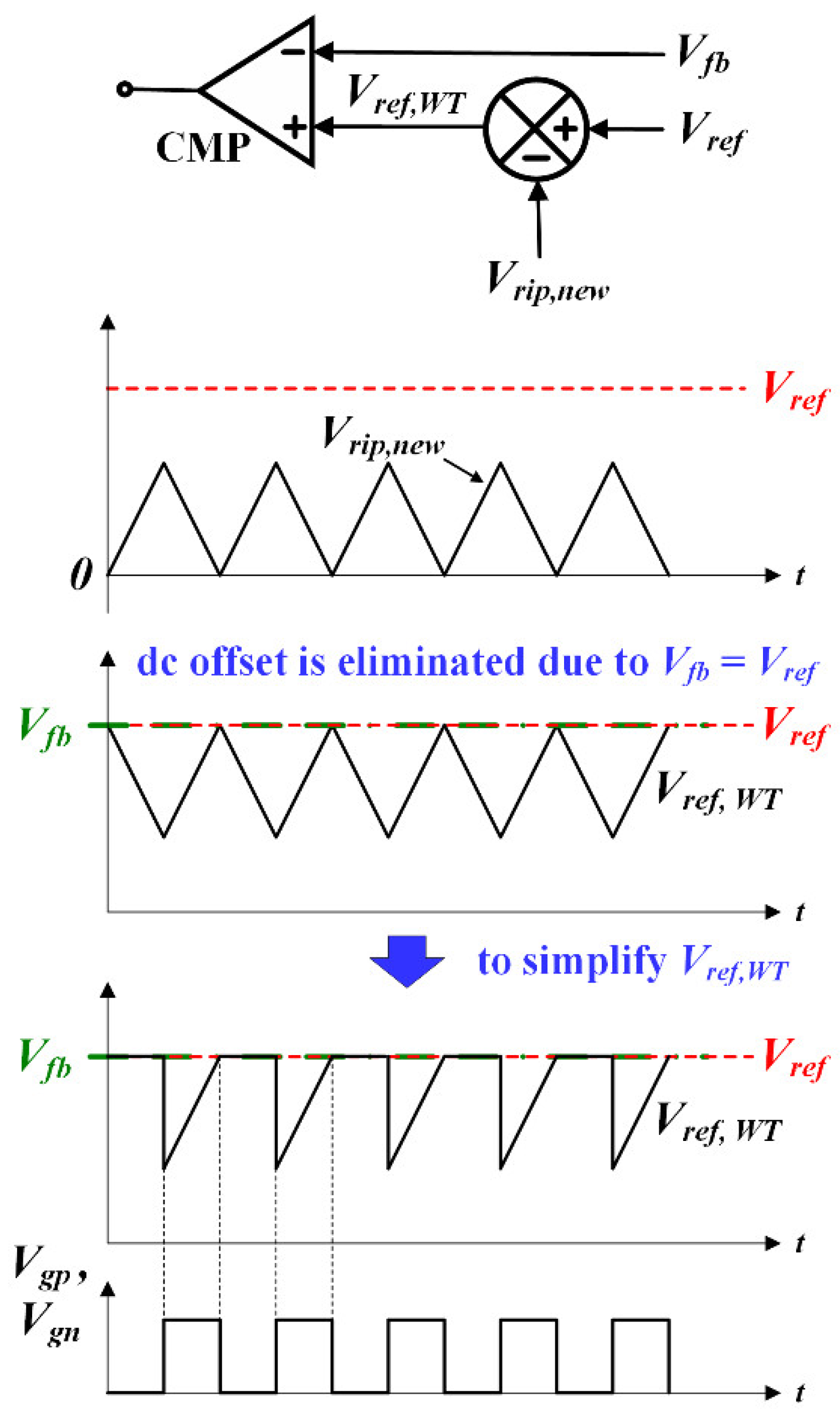
3.1. Wave Tracking Reference (WTR) Control
Figure 5 and
Figure 6 illustrate the concept of the VICR and WTR controls for the RBCOT buck converter. Assuming the ESR of a capacitor is sufficiently small, the ripple of
Vfb is ignored. For the VICR control,
Vsen,rip is added to
Vfb. Because the average value of
Vsen,rip is zero, for signal
Vsum, there is a 0.5
Vsen,rip difference between
Vref and
Vfb. Thus, the VICR control causes the output DC offset, as shown in Equation (4). In
Figure 6, by subtracting ripple signal
Vrip,new from the reference signal
Vref, system stability of the WTR control can be ensured. When the valley voltage of
Vrip,new is set to zero, the output DC offset is eliminated due to
Vfb and
Vref being identical. When power transistor
MP is turned on, its on-time period is controlled by the AOT circuit.
MP is turned on again when
Vfb is lower than
Vref,WT, and this instant happens during the off-time period. Thus,
Vrip,new requires information about the inductor current ripple only during the off-time period. As a result, the implementation complexity and power consumption of a sensing circuit can be reduced significantly. From
Figure 6,
Vref,WT is shown as
On the basis of the WTR control, the peak voltage
Vref,WT,peak is expressed as
From Equation (10), the output voltage can be derived as
where
K1 =
Rfb2/(
Rfb1 +
Rfb2). Similar to the VICR control,
Vrip,new should be set adequately large to ensure the system stability with WTR control. In contrast, the output DC offset with the WTR control is eliminated because
Vfb is equal to
Vref. As a result, the WTR control can concurrently improve DC accuracy and stability in an AOT controlled buck converter with low ESR.
3.2. Implementation of WTR Control
To implement the WTR control, a tracking reference generator is proposed, and its schematic and operation waveforms are illustrated in
Figure 7. When power transistor
MN is turned on, transistor
MN5 also turns on. During the off-time period, the source voltage of
MN5 is set to zero due to the negative feedback composed of operational amplifier
OP2 and transistor
MP6. Since the gate, source, and drain voltages of
MN and
MN5 are the same, the sensing current
Isen is produced by
MN5, and its value is proportional to the aspect ratio of
MN5 to
MN.
To generate a wave tracking current
Isen,WT and a DC current
Isen,dc from
Isen, as shown in
Figure 7b, the gate signal
Vsp of
MP6 is sent to the two sample-and-hold (S/H) circuits. When signal
QB, as shown in
Figure 4, changes from a low state to high state,
Isen starts from zero. During the rising period,
Isen does not reach the right level; thus, two delay signals
QB,d and
QB,dB, as shown in
Figure 4, are utilized for appropriate sampling. At the beginning of falling period for
Isen,
QB is already in a low state; hence, no delay signal is needed. The two S/H circuits are controlled by signals
Qsp,B and
Qsp, which are generated by
QB and the two delay signals
QB,d and
QB,dB. In the S/H circuits, when
Qsp,B changes to a high state, transmission gate
TG1 is turned on, and then
Vsp,WT tracks
Vsp.
TG1 and
TG2 are turned off and on, respectively, when
Qsp,B and
Qsp are in a low and high state. Subsequently, a DC level is kept on
Vsp,WT and
Vsp,dc.
Vsp,WT and
Vsp,dc are connected to the gate terminals of
MP5 and
MP4, respectively. Consequently,
Isen,WT and
Isen,dc are produced, as shown in
Figure 7b.
Isen,dc is equal to the valley level of
Isen,WT. By subtracting
Isen,dc from
Isen,WT, the off-time inductor current ripple is generated.
Operational amplifier
OP1, transistor
MN1, and resistor
R1 form a voltage-to-current circuit, and the current passing through
MN1 is equal to
Vref divided by
R1. Then, through a current mirror composed of transistors
MP1 and
MP2, a DC current
Iref is produced. To perform current subtraction, transistors
MN2 and
MN4 are used. Finally, the WTR signal
Vref,WT is realized and can be formulated as
Since Isen,dc is equal to the valley level of Isen,WT and R1 and R2 are the same, the peak voltage Vref,WT,peak and Vref are identical. Thus, the output DC offset is eliminated. Signal ENWTR is adopted to enable or disable the function of WTR control scheme. When ENWTR is in a low state, transistors MP3 and MN3 are on; hence, the WTR function is disabled and WTR signal Vref,WT is equal to Vref. Otherwise, the WTR function is active. Compared to the VICR control, the WTR control is implemented without any low-pass filter, trimming mechanism, or off-chip components, leading to smaller chip area without an additional IC pin.
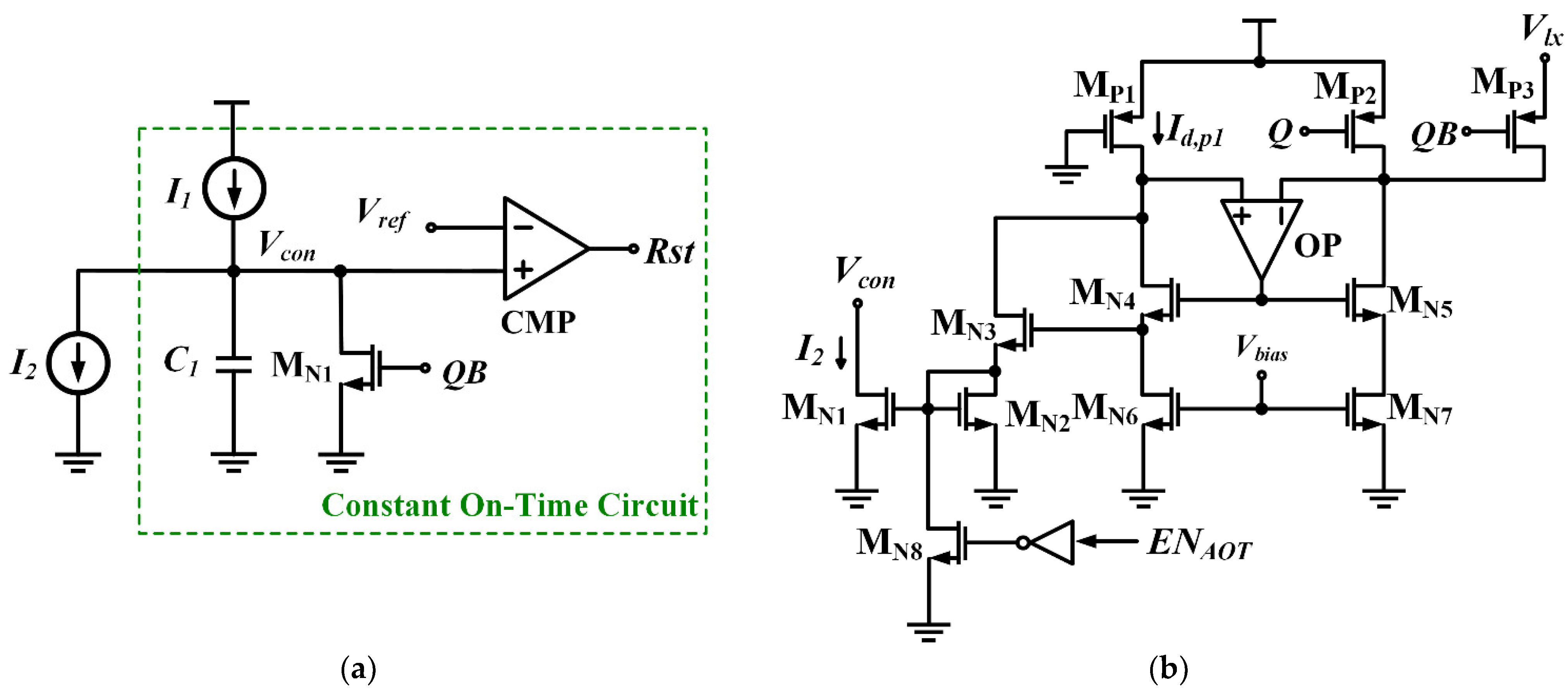
3.3. Adaptive On-Time (AOT) Circuit
For the RBCOT control, when the load current increases, the off-time period of power transistor
MP is diminished. Thus, the switching frequency is increased due to the fixed on-time period. To alleviate the variation on switching frequency in CCM in the case of load current changes, the AOT circuit is presented as shown in
Figure 8a. The AOT circuit consists of a constant on-time (COT) circuit and a sink current
I2. Since only an additional current
I2 is demanded, the AOT circuit is simple and results in a small silicon area and low power consumption. For the COT circuit,
I1 is maintained constant. When signal
QB changes to a low state, transistor
MN1 and power transistor
MP are turned off and on, respectively, and then
I1 starts to charge capacitor
C1. When voltage
Vcon reaches the reference voltage
Vref, signal
Rst is in a high state. Subsequently, transistor
MN1 and power transistor
MP are turned on and off, respectively. Then,
C1 is discharged to zero. Until
QB changes to a low state,
C1 is charged again. Hence, a constant on-time period is generated.
I2 is proportional to the load current. When the load current increases, the charging current following through
C1 is decreased, leading to a longer on-time period. As a result, the variation in switching frequency at different load currents is suppressed. The schematic of current
I2 is shown in
Figure 8b. When
Q and
QB are in high and low states, transistors
MP2 and
MP3 are off and on, respectively. Through the negative feedback loop, the noninverting pin of operational amplifier
OP is equal to voltage
Vlx. Thus, the gate, drain, and source voltages of transistor
MP1 and power transistor
MP are the same, and current
Id,p1 is proportional to the drain current of
MP. To ensure that most of current
Id,p1 passes through transistor
MN3, the current generated by transistor
MN6 should be set small. Through transistors
MN1 and
MN2,
I2 is generated. When power transistor
MP is off, transistor
MP2 is on, and then current
Id,p1 becomes zero for power saving. When signal
ENAOT is in a low state,
I2 becomes zero, and the buck converter operates with COT control. Otherwise, the buck converter operates with AOT function when
ENAOT is in a high state.
3.4. Stablility in the WTR Control
Referring to the proposed converter in
Figure 4 and the function of tracking reference generator in
Figure 7, the equivalent circuit model is shown in
Figure 9, which can be processed with a subtraction of two signals: one is from direct current feedback
Vsen,WT, and the other is the sensed DC current information
Vsen,dc after an LPF. The current sensing gain
Rsen is equal to
kR2, where
k is a value of current mirror and
R2 is the resistance shown in
Figure 7. According to the approach in [
8,
9], the transfer function
Gvr of reference to output voltage is derived in Equation (13) as the on-time period is small.
To get rid of converter instability, the poles must be on the left-half plane. Thus, Equation (14) is calculated since
Q1 needs to be larger than zero.
In the WTR control, the external current information equivalently increases the effective value of RESR by the factor of (Rsen/RESR + 1) to release the stability constraint of large RESR in a conventional COT converter. Without the WTR control, Rsen become zero. Hence, for conventional COT control, the product of the output capacitance and its ESR should be larger than half of the on-time period.
4. Experimental Results
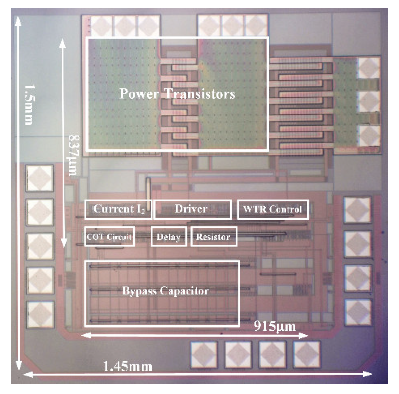
To verify the feasibility of WTR control and AOT circuit, a laboratory prototype of the proposed buck converter was built with an input voltage of 3.3 V, output voltage of 1.8 V, and maximum output current of 500 mA. The output inductance was 6.8 μH and the output capacitor was a 10 μF MLCC with an ESR of 4 mΩ. The proposed buck converter was fabricated with a standard 0.35 μm CMOS process. The chip microphotograph is shown in
Figure 10, and its core area was 837 × 915 μm
2.
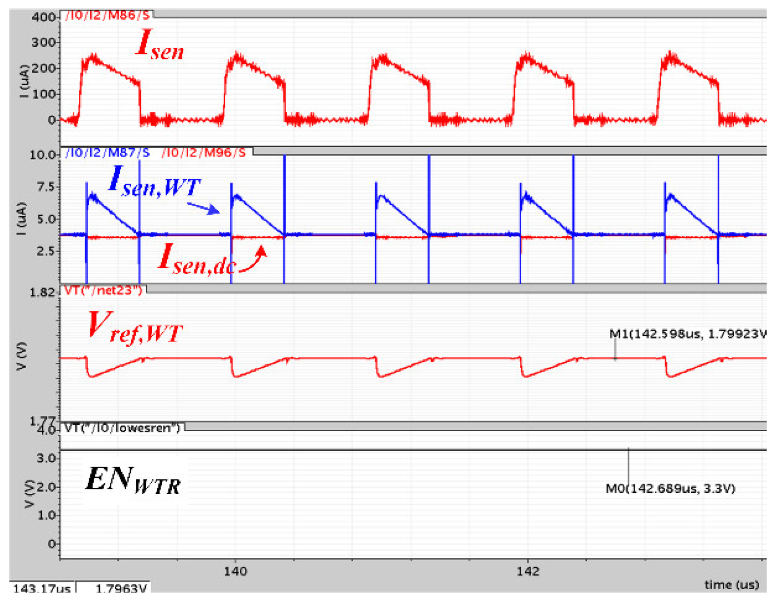
Figure 11 shows the simulated waveforms of the tracking reference generator. The sensing inductor current
Isen, waveform tracking current
Isen,WT, DC current
Isne,dc, and WTR signal
Vref,WT can be found in
Figure 7. When signal
ENWTR was in a high state, the tracking reference generator was enabled. It can be noted that current
Isen,WT and current
Isne,dc were the same during on-time periods. There were spikes in signal
Isen,WT due to the operation of the S/H circuits, but these spikes did not affect the WTR control operation. The waveforms coincided with the circuit analysis in
Section 3.2.
Figure 12 and
Figure 13 show the measured waveforms of the buck converter with the WTR control at load currents of 100 and 500 mA, respectively. The output voltage of the buck converter was kept at 1.8 V, and the output voltage ripple Δ
Vo was as small as 3 mV. This means that the WTR control could ensure the stability of the buck converter with ripple base control.
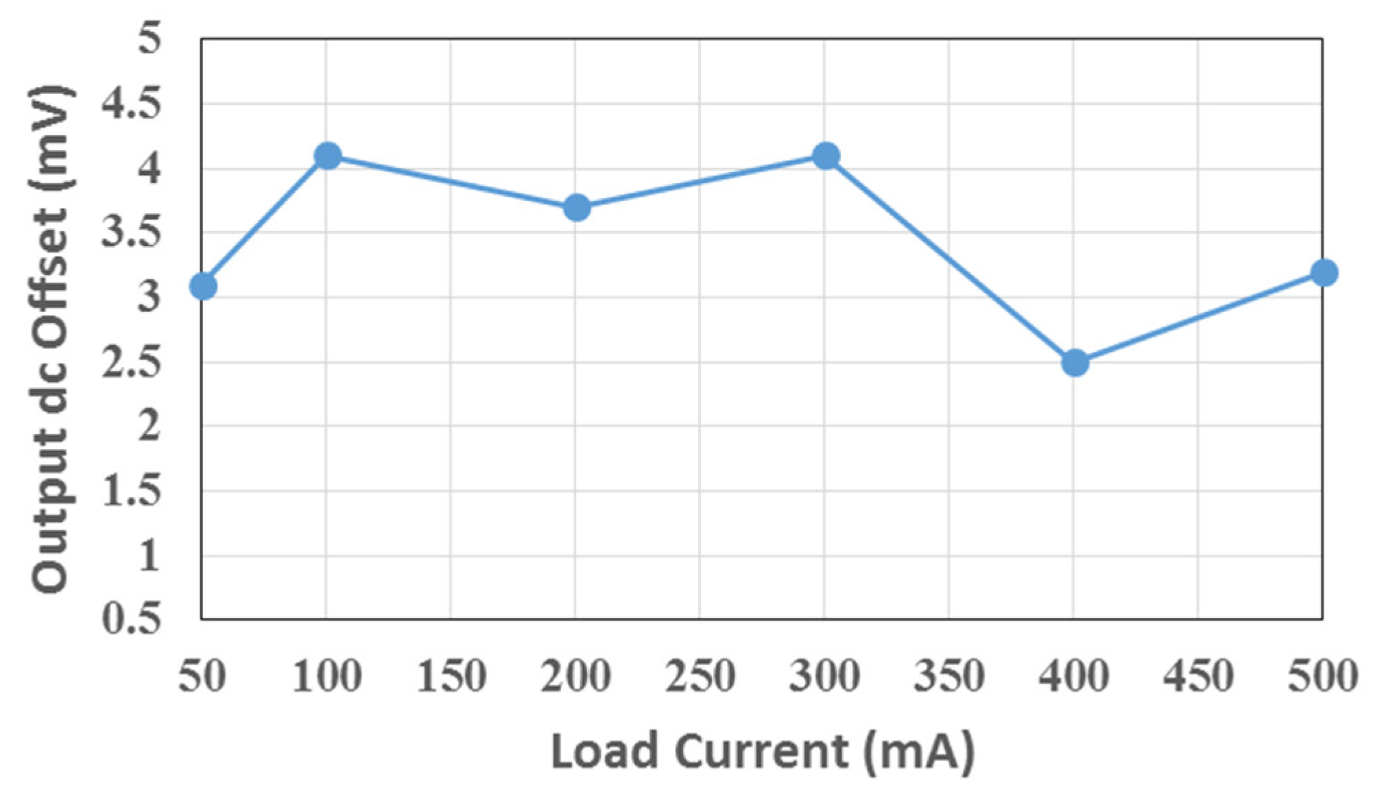
Figure 14 plots the measured output DC offset with the proposed control when the load current changed from 50 mA to 500 mA. The maximum DC offset of the proposed converter was 4.1 mV.
Figure 15 shows the measured transient waveforms of the proposed buck converter for the load current changing between 450 mA and 50 mA. For a step-down load, the proposed buck converter took 4 µs to resume its regulated value with a transient ripple of 50 mV. Furthermore, the output voltage levels at two different load currents were the same. The recovery time and transient ripple of the buck converter were 9 µs and 100 mV for a step-up load.
Figure 16 plots the switching frequency of the buck converter versus load currents without and with AOT function. It can be found that the differences in switching frequency without and with AOT function were about 79 kHz and 11 kHz, respectively. The switching frequency with AOT control was kept approximately constant at different load currents.
Figure 17 plots the measured efficiency of the proposed converter when the load current changed from 50 mA to 500 mA. The maximum efficiency of the proposed converter was 90.9% at a load current of 200 mA. A comparison of results with previously proposed on-time controlled buck converters is summarized in
Table 1. The performance of
fsw variation is indicated by (Δ
fsw/
fsw) and (Δ
fsw/ΔI
Load). The performance of the proposed buck converter was comparable to those with different control techniques.
5. Conclusions
An RBCOT buck converter with VICR control can relax the stability constraint of a large ESR at the output capacitor, but the output regulation accuracy is degraded due to output DC offset. Moreover, the switching frequency of the RBCOT buck converter varies with load current changes. Therefore, in this paper, WTR control was proposed for MLCC to improve converter stability while eliminating DC offset on the regulated output voltage. The WTR control was implemented without any low-pass filter, trimming mechanism, or off-chip components compared to the VICR control. Since the AOT circuit was utilized to suppress the switching frequency variation in CCM at different load currents, even without clock-controlled circuits, the buck converter operated with a nearly constant switching frequency. The test chip was fabricated in a 0.35 µm CMOS process for validation. The experimental results showed that the maximum output DC offset was 4.1 mV and the output voltage ripple was as small as 3 mV, while the recovery times were 4 µs and 9 µs for step-down and step-up loads. Furthermore, the switching frequency variation was 11 kHz when load current changed from 50 mA to 500 mA, and the measured maximum efficiency was 90.9%.


