1. Introduction
Power generation, transmission, and conversion make up a complex process that requires the interconnected operation of various components in a power system. Reactive power is one of the main components of the system. To improve the performance of AC power systems, this reactive power has to be managed. This is known as reactive power compensation. For this purpose, various kinds of compensation devices are applied in AC power systems.
Typically, the current in old-fashioned power distribution lines lags behind the voltage, because of the presence of inductive loads such as motors [
1]. Local reactive power compensation devices are usually designed to compensate the lagging reactive power. The application of energy-efficient light emitting diode LED lighting sources reduces the power demand by about 30% relative to the currently available sources. Unfortunately, these systems are, in many cases, the source of disturbances that further reduce the power factor. The evolution of LED light technology and variable frequency drive (VFD) technology has changed the type of reactive power available in 0.4 kV power distribution lines.
The problems posed by modern LED light sources have been examined in previous publications [
2,
3]. The authors of [
2] state that LED light sources generate leading reactive power. Their publication presents current and voltage diagrams and measured power values to prove this. However, they did not analyze the reasons for this or take into account the specific details about the voltage converters present in LED light sources. They stated that the use of LED lighting reduces the use of real power, but increases the generation of leading reactive power, which causes compensation problems. The authors of the publication suggest stricter standardization of the power factor values of the converters used in LEDs. In [
3], an analysis of other aspects of LED application is conducted, and LED current and voltage diagrams showing that LED light sources generate leading reactive power are given. The publication only presents experimental measurements and does not analyze the theoretical causes of leading reactive power generation. The authors of [
4] use connected fixed setting inductors in lighting control cabinets to compensate for the reactive power produced by street LED lighting sources. However, this requires additional costs and an increase in the consumption of non-ferrous metals. The authors of [
5] propose a distribution static synchronous compensator integrated with a Y-y connection transformer for reactive power compensation. This can compensate for both leading and lagging reactive power.
Recently, the VFD-based on a novel three-phase purely semiconductor matrix converter (MC) has become increasingly popular. The purely semiconductor-based MC does not require intermediate energy storage capacitors. With the rapid development of semiconductor technologies, the MC’s popularity has been constantly increasing. In the MC-based VFD, Indirect Space Vector Modulation (ISVM) can be applied. ISVM considers the MC to be of the indirect form, featuring a Current Source Rectifier (CSR) part and a Voltage Source Inverter (VSI) part. This virtual division enables the direct control of the phase angle between the MC input current and voltage, while allowing for the direct control of the reactive power at the point of connection to the power distribution lines. Based on this principle of functioning, the MC-based induction motor VFD has the ability to exchange both leading and lagging reactive power with the connected power distribution line. This means that the MC-based induction motor VFD could be used for LED wall display generated reactive power compensation.
Additionally, MCs have two obvious advantages over conventional capacitor-based local compensation devices. Firstly, the use of large capacitor banks can be avoided. This is an advantage from the point of view of volume and reliability. Secondly—along with reactive power compensation, the MC can perform their primary function of induction motor powering and speed control.
Some authors of reviewed publications have suggested that the ISVM-controlled MC should be used for reactive power compensation. It has been suggested the use of a permanent magnet machine powered by a MC as the compensation device [
6]. In [
7], reactive power ripple minimization in matrix converter-fed double-fed induction generators is presented. The authors of [
8] present a modulation strategy to extend the reactive power transfer range in the MC. The only study that has taken the reactive power in the MC VFD induction motor into account is [
9]. However, the authors of this publication only propose a control strategy that provides current control and a power factor close to unit. They did not measure the ability to compensate the reactive power produced by LED wall screens.
After assessing the listed problems and previously performed research, the following study aims were generated:
To study the nature and value of the reactive power generated by LEDs with respect to the effect of harmonics;
To explore the possibility of using matrix-converter-based variable frequency drives to compensate for this reactive power;
To investigate a way to extend the reactive power compensation range.
2. The Effect of Harmonics on Power Factor
The reactive power measurement of a nonlinear load can be performed with or without taking the effect of harmonics into account.
In mathematical terms, the relation is as follows:
where
Q is the displacement of the reactive power at the fundamental harmonic,
PF is the power factor, and
S is the total power.
However, most of older measuring devices do not emit these powers and determine only the total amount of reactive power
QT, before which also adds the reactive power
D generated by harmonics:
where
DPF is the distorting power factor and
D is the distorting reactive power of a higher harmonic.
It should not be forgotten that, in non-sinusoidal AC systems, there is a difference between the displacement power factor Q (PF or cos φ) and the distorting power factor D (DPF). This power has an immediate effect on the waveform and the THD of the current. However, most measuring devices do not emit these types of power and just determine the total amount of reactive power Q, which also includes the reactive power D generated by harmonics.
In the reactive power compensation process, the displacement reactive power and distorting reactive power of harmonic are compensated differently. Power factor correction equipment is not of any use, because it only acts on the displacement reactive power Q. The distorting reactive power of harmonic D is reduced using filtering equipment.
In the industry, the focus is on compensating Q, as fines are paid for non-compensated Q. Less attention is paid to D compensation by the industry, because there is no penalty for D generation.
Recently, more and more devices with non-linear rectifiers and switched converters have been connected to distribution lines. Nonlinear loads and switched devices energized by sinusoidal sources produce Q and D together. This causes specific compensation problems. Conventional capacitor-based compensating devices are designed to compensate for the positive signal reactive power Q. Therefore, it is necessary to determine the sign of reactive power Q generated by such loads and the requirements for compensation. Reactive power in power distribution lines today
Typically, current lags behind voltage in conventional power distribution lines, because of the presence of inductive loads such as AC motors. However, as shown in
Figure 1, more and more power consumption devices are being developed that influence the power distribution lines via a diode rectifier. These are the conventional diode rectifier supply-side VFD, LED lighting sources, and others. These diode rectifier supply-side devices can be divided into two groups: -with and without the power factor correction (PFC) function.
2.1. Performance Features of Diode Rectifier Supply-Side Devices without the PFC Function
As shown in
Figure 2, a typical LED power supplier consists of a diode rectifier, a DC circuit electrolytic capacitor, and a DC/DC converter for voltage adaptation. The reactive power of such equipment directly depends on the voltage at the power distribution line connection point and the input current of the rectifier.
The voltage pulsations and current of diode-rectifier-based devices can be expressed by the following equations:
when
ωt is in the range [
α, π/2] and [π +
α, 3π/2], otherwise,
iIN = 0.
where
VPDL is the voltage of power distribution lines;
IIN is the input current of the LED supply;
VM is the voltage amplitude;
C is the rectifier capacitor value;
VOUT is the rectifier capacitor voltage;
VMIN is the minimal voltage value at the rectifier capacitor terminals; and Δ
VPULS is the amplitude of the voltage pulsations. According to the technical requirements, the voltage pulsation
kV of the filter capacitor is in the range of 5 ÷ 10%. Based on this value, time
α is set when the current starts to flow through this capacitor:
The produced reactive power:
Due to the large number of harmonics, the input current of a diode-rectifier-based device has a fairly complex expression:
The consumption or generation of reactive power depends on
. Because of this it must be expressed in the Fourier line and the
must be determined.
Based on the previously written equations:
In the case of α1 = 64°, φ1 = 19.1°;
In the case of α2 = 72°, φ2 = 16.1°.
These are the minimum and maximum limits of the current displacement angle. Since φ1 > 0 and φ2 > 0, it can be stated that the diode rectifier supply-side devices inject some of the leading reactive power into the power distribution lines. The amount injected is 0.28 ÷ 0.34 kVar when 1 kW load is being powered. This reactive power cannot be compensated for with a conventional capacitor-based local compensation device.
2.2. Performance Features of Diode Rectifier Supply-Side Devices with PFC Function
Recently, special power supplies with PFC correction components have been increasingly used for low-power sources, especially LED lamps. As shown in
Figure 3, these power supplies are supplemented by the specialized power factor correction block: -its operation is described below. An example is the L6562D—controlled rectifier presented in
Figure 4. The L6562 is a current-mode PFC controller that operates in Transition Mode. This highly linear multiplier includes a special circuit that is able to reduce the AC input current distortion, allowing a wide range of mains operations to be carried out with an extremely low THD, even over large load ranges [
10].
When the converter is ON, the tactical frequency generator A3 transfers a pulse via D1 to trigger D2. A high voltage level occurs at the location of trigger D1 output, and the transistor switcher T1 is turned ON. As a consequence, the current across L1 and T1 increases. The current through resistor R3 increases and is fed to one input of comparator A5 input. A signal, proportional to the voltage of power distribution lines, is applied to the next A5 input from the multiplier R1-R2. When the UCUR exceeds the A4 output voltage, the comparator A5 changes the polarity and T1 is moved to the OFF state via D2. The current IL1 flows through D1 to the load, where it decreases. When IL1 = 0, the zero value finding unit A1 generates a signal, which moves T1 to the ON state again via D1, the process is repeated. As the proportional values of VIN and UCUR II are compared, this current IT1 reproduces the shape of the power distribution line voltage. The output voltage UOUT depends on the multiplier A4 transmission factor. In this way the VOUT = const is maintained. Because the input current reproduces the shape of the power distribution lines voltage, the THD is close to zero. However, the filter capacitors CF1 and CF2 are required for smooth operation of the converter. This shows that elimination of the harmonics worsens the power factor.
In the typical L6562D circuit provided by the manufacturer, only the capacitors
CF1 and
CF2 and the inductance
L are recommended for use, but in practice, the use of these elements significantly increases the power factor of the device. The manufacturer offers the following filter component values for the L6562D controlled 80 W power device:
CF1 = 0.47 µF,
CF2 = 0.68 µF, and
L = 47 mH [
10]. The reactive power is leading and displacement angle of such a device is
Qc = −19 var,
φ = 13.1°: so a significant negative power factor is obtained (0.97). However, such a power factor will only occur with a rated source load. If the load is lower than the nominal value, the power factor will be much worse.
2.3. Experimental Comparison of LED Power Supplies with and without PFC Function
In order to experimentally research the reactive power generated by LED power supplies, two power supplies, from the same manufacturer were researched. Both LED power supplies produced 60 W. The first LED power supplies had a conventional design-connected to power distribution lines via a conventional diode rectifier. The second LED power supply was supplemented by components with the ability to perform the PFC correction function.
A comparison of the input current curves of the two LED power supplies shows that they differ significantly. Oscillograms of the input current curves of both LED power supplies were obtained during the study and are presented in
Figure 5. A comparison of these curves shows a fundamental difference between the conventional LED power supply and one with the PFC correction function. The power quality analyzer MI2892 was used to analyze the power quality at the point that these blocks connected to the power distribution lines. Using this analyzer, it was possible to measure the distorting power factor DPF, the total amount of reactive power
QT, and the total amount of complex power
St. The measurement results are presented in
Table 1 and
Table 2.
The measurement results, which were applied to the conventional capacitive rectifier-based LED power supplier, confirm our theoretical assumptions. The measured total reactive power was an average of 30 percent of the real power. At low or zero load, the reactive power increased due to interference from the filtering capacitors. Thus, in the presence of a large number of these LEDs, the reactive power of the power supply would become significant causing the need to compensate for it. Since the current of the LED power supplier is non-sinusoidal, high values of ST and QT were obtained, much higher than those of Q and S.
The measurement results, which were applied to the LED power supplier, showed that the total reactive power was an average of 30 percent of the real power. Due to the installed PFC correction function components, the input current was close to sinusoidal.
Figure 5 show that the input current had a displacement angle related to the voltage of the power distribution line, which was the cause of reactive power. At low load currents, the capacitance of the input filter significantly affected the formation of the displacement angle, but at high loads, the displacement angle formed due to other reasons. The measurement data show that the filter capacitor in this unit was much smaller than recommended—the reactive power with no load was only −4 var. This could have been due to the operation of the internal element A4 (multiplier) of the chip. In the initial capacitor charging stage, the capacitor was charged to the required voltage by sinusoidal current in about 5 ms. In the next stage, the A4 transmission rate was reduced because a constant voltage needed to be maintained in the capacitor. Therefore, the input current dropped faster than it rose, and a current displacement occurred with respect to the voltage. This was necessary to allow the capacitor to maintain a constant voltage or become fully charged. If that shift was avoided, it would be quite difficult to predict the value of the A4 transfer factor based on several converter mode parameters. However, manufacturers are adopting a simpler option. The harmonics distortion of this LED power supply unit was small compared to that of other power supplies. Its
S and
Q were almost indistinguishable from
ST and
QT, so the negative effect of harmonics distortion was reduced. Our experimental studies showed that the same reactive power compensation problems occur with both the capacitive rectifier-based LED power supplier and the LED power supplier with the PFC correction function.
2.4. Reactive Power of Parallel Connected LED Power Supplies
Connecting a group of identical diode rectifier supply-side devices to power distribution lines has been shown to have an even more significant impact on the power factor. This was confirmed by measurements made in a large arena building with a 32 kW LED wall display powered by dozens of small LED power suppliers with a PFC function. Like a single LED power supplier with a PFC correction function, the whole combination also generates leading reactive power. This poses serious problems for reactive power compensation, as the interaction of the LED with a conventional capacitor-based local reactive power compensation device leads to overcompensation.
Figure 6 shows the active and reactive power values caused by this wall display. These data were collected from the Kaunas “Zalgiris” arena, where a DA80.1600RGB-50M LED wall display is installed. The data were collected in full daylight, as the brightness of the screen was the highest at that time. The data show that, regardless of the real power consumption, the LED wall display produced a leading reactive power Q in the range of 9.5–10.9 kVar. Due to overcompensation by the old-fashioned capacitor-based local reactive power compensation device, the company that operates this sports arena pays fines to the electric power supply company.
In both cases a universal compensation device is required, which has the ability to compensate for both types of reactive power: leading and lagging.
Next, we describe the use of an induction motor powered by the MC as a universal compensation device. Depending on the structure of the converter and the specific controls, it can be said that the MC-based VFD may be suitable for both leading and lagging reactive power compensation.
3. Special Features of the Matrix Converter-Based Variable Frequency Drive
The researched compensation device consists of the MC, whose input is connected to the power distribution lines and powers the induction motor (
Figure 7). The MC is a forced commutated converter, that consists of nine bidirectional switches as the power elements to create a variable output voltage system. In contrast to the conventional VFD, the MC-based VFD contains no large energy storage elements (capacitors). The key element of the MC is the fully controlled four-quadrant bidirectional switch, which allows high-frequency operation. There are 27 possible combinations (vectors) for the bidirectional switches of this three-to-three phase matrix converter.
With an MC, Indirect Space Vector Modulation (ISVM) can be applied to control output voltage and input current. The ISVM considers the matrix converter to be of the indirect form. It features a Voltage Source Inverter (VSI) control part, a Current Source Rectifier (CSR) control part and a DC link in between.
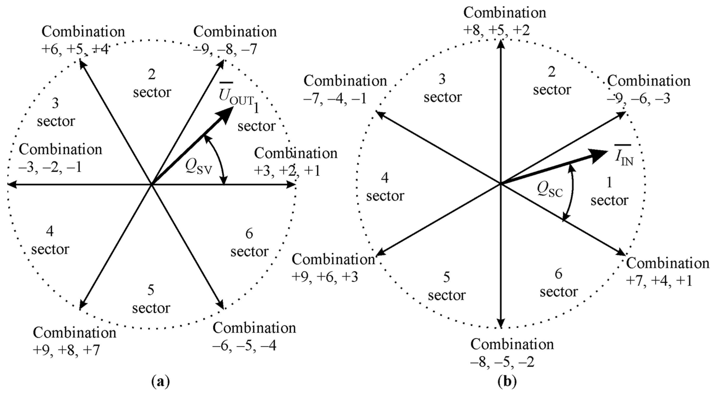
By using the ISVM strategy, the desired output voltage and input current are synthesized from the active vectors and zero vectors. As shown in
Figure 8, the active vectors are formed from 18 possible switch combinations (−9, −8, …., +8, +9).
The two adjacent vectors approximate the space vector of the desired output line voltages and input currents. The frequency of the MC output voltage is determined by the angle
QSC, and the input current displacement is determined by the angle
QSV.
where
t is the time, determined through synchronization with the frequency of the power distribution lines and
φin is the preferred current displacement angle, which determines the reactive power at the area of input of the MC.
The control algorithm used for vector approximation is presented in
Figure 9. According to the ISVM control strategy, it consists of two sequences representing the rectifier and inverter stages. Every sequence consists of sector determination and duty cycle determination. Both sequences are combined by the common duty cycle determination segment and bidirectional switchers control logic, as presented in
Table 3.
When
dα,
dβ = 1 (stage of VSI is Off), three DC voltages
VDC1-3 will be generated at the MC output. These voltages are presented in
Figure 10. Based on these voltages, the VSI stage forms the sinusoidal output voltages
VoA−
VoB.
The ISVM ensures a voltage transfer rate of 0.866, but this value is not satisfactory for induction motor stator windings connected in a “star” formation. Therefore, only the “delta” connection is applicable for the MC-based VFD.
4. Application of the Matrix Converter-Based Variable Frequency Drive as the Reactive Power Compensation Device
By using the MC-based VFD, the transfer of real power to the motor and the reactive power compensation are performed simultaneously. In order to determine the reactive power compensation range, the system, whose structure is presented in
Figure 11, was researched through a Matlab/Simulink simulation.
The input current and output voltage of this converter can be described by the following equations:
where
is the MC input current,
is the MC output voltage,
m is βthe modulation index,
is the input displacement angle, and
is the output displacement angle.
There are no storage elements in the matrix converter, and the matrix converter is considered lossless in this analysis. From Equations (19) and (20), it is possible to write an equation to show the amount of power in the MC:
From Equation (21), it can be seen that an increase in the output displacement angle φOUT causes a decrease in the MC input current IIN. It can also be seen that an increase in the input displacement angle φIN causes a decrease in the MC output voltage VOUT.
Equation (10) shows that the load power of the MC must have a constant value, thereby ensuring the correct operation of the MC and the induction motor. To ensure constant load power
POUT when cos
φIN is variable, it is necessary to have a certain range of output voltages regulation. In such a case, a constant
POUT would be maintained during the control of the modulation index
m (0 ÷ 1).
The cos
φIN value is limited when
m = 1:
For the induction motor powered by the MC to be applied as a flexible AC transmission system device, the voltage VOUT at the induction motor stator windings less then the input voltage by √3. Because of this, the stator windings have to be connected in a “delta” Δ format.
The voltage ratio to ensure reactive power compensation:
Equation (26) is only valid if the MC output voltage frequency is equal to the frequency of the power distribution line voltage. In the event that the MC output voltage frequency is not constant, the condition is:
In the case of
fOUT = 25 Hz,
As shown in Equation (29), the output power decreases by almost half, reducing the output voltage frequency. However, this decrease is offset by an increase in tan ϕ1N limf. Therefore, MC’s has the ability to compensate for reactive power increases with a decreasing output voltage frequency.
4.1. Matlab/Simulink Model of the Induction Motor and the Matrix-Converter-Based Reactive Power Compensation Device
The Matlab/Simulink model of the researched system consists of four parts. The first part contains the simulation blocks of the power distribution line components for a 10/0.4 kV transformer. Matlab/Simulink blocks the implementing ideal sinusoidal AC voltage source and therefore a three-phase series RLC branch was used.
The second part contains nine ideal bidirectional switches from the MC and ISVM control modules. For the simulation of the nine bidirectional switches, the Matlab Simulink blocks the implementation of IGBT device and a diode in parallel through a series RC snubber circuit shown in
Figure 12.
The third part contains an MC load, which is presented as an equivalent diagram of the induction motor [
11].
For the power measurements the PLL-Driven, Positive-Sequence block was used. This computes the positive-sequence real power P (in watts) and the reactive power Q (in vars) of a periodic set of three-phase voltages and currents.
4.2. The Reactive Power Compensation Ranges of the Induction Motor and the Matrix-Converter-Based Compensation Device
For the MC-based VFD, the reactive power is presented as a function of the current displacement angle in
Figure 13. The values of reactive power were determined by keeping the real power transferred to the motor constant. As a result, changes in real power caused by current displacement angle changes (rectifier stage) were compensated by voltage modulation index correction (inverter stage). The MC was powered by 400 V of line-to-line voltage. The induction motor stator windings were connected to the MC output in “delta“ format to allow adaptation to 230 V line-to-line powering. By connecting the MC and stator windings in this way, it was possible to perform reactive power compensation. Consequently, at a displacement angle of zero, the modulation index must be significantly reduced. However, by when the displacement angle increased, there was a much wider voltage correction range due to the delta connection.
Figure 13 clearly shows that the reactive power can be compensated in both directions (leading and lagging), depending on the current displacement angle.
In case of stator windings “delta“ connection the range of possible displacement angles is from minus 44 degrees to plus 47 degrees. These angles allow the real power transferred to the motor to be kept constant. For 15 kW induction motor, the reactive power produced at these displacement angles varies from the leading 14.7 kVar to the lagging 15.7 kVar. Increasing the displacement angle above this specified range will lead to a decrease in the voltage at the induction motor stator windings and a decrease in the real power transferred to the induction motor.
As presented in
Figure 14, the voltage drop due to the displacement angle change was recovered by increasing the value of the modulation index. Upon reaching the limits determined by displacement angel specified range, the modulation index reaches its maximum value and cannot recover a voltage drop caused by a further increase in the current displacement angle.
4.3. Matlab/Simulink Model of the LED Wall Display Loaded Power Distribution Lines
The 32 kW LED wall display described in
Section 2 produces an average leading reactive power of 10.15 kVar. In order to determine the ability of the MC-based VFD to compensate the reactive power produced by the LED wall display, a Matlab/Simulink model for the system MC-based VFD and the LED wall display was created. As shown in
Figure 15, the Matlab/Simulink model consist of two device models connected to power distribution lines—the 32 kW LED wall display with a PFC power supply model and an MC-based VFD model. The actual 32 kW LED wall display described in
Section 2.4 consists of 16 blocks connected to each of the three power distribution lines phases. Therefore, the LED wall display Matlab/Simulink model consists of 3 × 16 blocks.
To accurately reproduce the input current of the LED wall display, the model of each block consists of 16 components simulating the first 15 harmonics, and the DC component is presented in
Table 4. The second part of the model, MC converter, operates as the converter for the VFD, simultaneously, as the device for the reactive power compensation at the point of connection to the power distribution lines.
4.4. Compensation of the Reactive Power in the Distribution Lines
The ability to compensate for the reactive power generated by an LED wall display using standard rated asynchronous motors was investigated through a simulation. The possibility of using 5.5 kW, 4 kW, and 2.2 kW MC-based VFDs for this purpose was investigated. VFDs with these power levels were selected, because induction motors with these power levels are found in the air handling units of buildings and are connected to the same power distribution lines as the LED wall display. Therefore, the simulation results can be used to guide the real implementation of such a compensation system in the arena building. As can be seen from the simulation results presented in
Figure 16, only the 5.5 kW VFD showed the ability to carry out complete reactive power compensation. The power factor is equal to the unit available with the 5.5 kW MC-based VFD at the current displacement angle of minus 42.6 degrees.
It was found that the 4 kW and 2.2 kW rated power MC-based VFDs cannot compensate the power factor to unit. After lowering the current displacement angle below minus 44 degrees, the 4 and 2.2 kW MC-based VFDs were no longer able to maintain the voltage required on the stator windings and constant power transfer to the induction motor.
Figure 17 shows how the reactive power generated by an MC-based VFD depends on the current displacement angle. This figure also shows how the reactive power changes at the point of connection of the VFD to the power distribution lines when the reactive power of the LED display is constant.
5. Discussions
The idea for this research came from the fact that the interaction of a large number of LED lighting sources with a conventional capacitor-based local compensation device leads to overcompensation in the 0.4 kV power distribution lines. This is due to the fact that the conventional compensation device is designed to compensate the lagging reactive power produced by inductive loads, such as AC motors. This highlighted the demand for compensation of capacitive reactive power which is not predicted by the designer.
The application of matric converter based-VFD could solve the problem of compensating the reactive power generated by LED devices. In addition, the application of these VFD allows the use of compensation devices with large inductors to be revoked. In addition, matric converter based-VFD can be useful if there is a need to compensate lagging reactive power produced by inductive loads, such as induction motors. Applying matric converter based-VFD for lagging reactive power compensation could eliminate the use of large capacitor-based compensation devices.
In further research we plan to investigate the possibility of using a conventional AC-DC-AC converter and a Back-to-Back converter based-VFD to compensate for the reactive power in power distribution lines. The low power conventional AC-DC-AC converter based-VFD has the structure similar to that of LED power supplies. Therefore, a similar effect on reactive power can be observed.
6. Conclusions
Due to the special properties of LEDs, the interaction of LED lighting with conventional capacitor-based local compensation devices results in overcompensation in 0.4 kV power distribution lines. Experimental study of the harmonic structure of the input current of a LED power supply revealed that due to the specific harmonic distortion that occurs, leading reactive power is generated.
An application of the ISVM provides an opportunity to control the input current displacement angle of the MC-based VFD. As a result of this, the MC-based VFD could be applied for reactive power compensation, simultaneously, performing the main function of the VFD—motor powering and speed control.
An increase in the MC-based VFD input current displacement angle results in a decrease in the voltage of the stator windings below the nominal level. To recover this voltage decrease, the ISVM factor must be increased accordingly. Reactive power compensation can only be performed by connecting the stator windings in delta formation of 230/400 V motor. In the case of windings connected in a star formation, it is not possible to manipulate the current displacement angle, because there is no room to reproduce the voltage drop by changing the modulation index. The determined applicable range of the current displacement angle is from minus 44 degrees to plus 47 degrees in a delta connection formation. The asymmetry of the compensation range is related to the influence of the inductance of the motor windings.
The induction motor powered by the matrix converter has the ability to compensate the reactive power produced by the large LED wall display investigated in this study that cannot compensated by capacitors based local reactive power compensation device. The 10.15 kVar capacitive reactive power generated by the LED wall display can be fully compensated (power factor equal to unit) with a 5.5 kW induction motor powered by the MC keeping the current displacement angle of the ISVM minus 42.6 degrees. The voltage modulation index of ISVM in that situation is 0.96.
A MC-based VFD operating as a lagging reactive power compensation device has another obvious advantage over the capacitors based compensation devices—there is no need for any large capacitor banks. This is an advantage in terms of volume and reliability.
In this study, pure MC-based VFD without harmonic suppression components were investigated. Further work includes the study of the influence of MC harmonic suppression filters on the reactive power.


