1. Introduction
A surge arrester is a device widely used to protect electrical equipment from over-voltages due to lightning and switching operation in electrical power and telecommunication systems [
1]. The arrester exhibiting dynamic and nonlinear characteristics diverts current to the ground to clamp the over-voltage to be lower than the insulation level of the protected high voltage equipment. To confirm the performance in over-voltage mitigation, the international standards [
2,
3,
4,
5] advise performing residual voltage tests on the arrester.
According to the standard [
3] and in the residual voltage tests, four kinds of impulse current waveforms, i.e., steep impulse current (1/20 µs), high impulse current (4/10 µs), lightning impulse current (8/20 µs), and switching impulse current (30/80 µs), in different current peaks are injected to the arrester during tests. The residual voltages across the arrester associated with the different impulse current waveforms and peaks are examined. The impulse currents can be generated by a simple resistance, inductance, and capacitance circuit as illustrated in
Figure 1. The current generation circuit is composed of the DC voltage source (
Vs), the charging current limiting resistor (
RL), the charging capacitor (
C), the spark gap (
G), the series inductor (
Le), the series resistor (
Re), the shunt current measuring resistor (
RSH), and the surge arrester (
SA).
The most essential problem in residual voltage tests is that it is quite laborious for test engineers to generate an accurate waveform and a current peak according to the standard requirement, because the uncontrolled parasitic impedance in the current generation circuit and the nonlinear characteristic of the arrester affect the current waveform significantly. Therefore, an accurate arrester model is necessary to use in controlling the current waveform. There are a lot of researchers developing the accurate model used for designing insulation coordination and for obtaining successful high-voltage testing [
6,
7,
8,
9,
10,
11,
12,
13,
14]. Furthermore, the effect of thermal stress under the arrester operation and experimental tests can be included in the model successfully [
15]. However, the generation circuit and parasitic impedance are neglected in the process of model construction. It leads to the models not being appropriate in the residual voltage test in real practice. Therefore, trial and error approaches for selecting the circuit parameters and the charging voltage are still necessary to employ in the real experiment. Several experiments for waveform adjustment are carried out to obtain the required waveform and it sometimes unintentionally causes damage on the arrester during the test. It will be advantageous for test engineers if an effective technique for selecting the circuit parameters and the charging voltage is developed.
This paper aims to propose a simplified and accurate model of a surge arrester and an effective technique for selecting the circuit parameters and the charging voltage to obtain the specified impulse current waveform in residual voltage tests. Moreover, the residual voltage associated the impulse current waveform is estimated precisely. With the help of a genetic algorithm, the unknown parasitic impedance was determined, and the other appropriate circuit parameters and the charging voltage can be selected. The validity of the proposed technique was verified by the experiments for determination of the appropriate current circuit parameters, the charging voltage, and the residual voltage associated with the specified current waveform. From comparison of the experimental and simulated results, it was confirmed that the method is fairly highly accurate and very effective in the residual voltage tests of surge arresters. From this achievement, the proposed method is also very useful for the significant reduction of unintentional damages to the arrester during the process of waveform adjustment.
2. Conventional Surge Arrester Model
There are many proposed models of surge arresters but most of them are not applicable in residual voltage tests since the parasitic impedance and generation circuit are not taken into account in the process of model construction. For the sake of clarity, an experiment of the residual voltage test on a surge arrester with the rated voltage of 9 kV and the nominal discharge current of 10 kA was considered as a test case. As shown in
Figure 1, the setting circuit parameters in the experiment were composed of the charging capacitance of 2 µF, the series resistance (
Re) of 0.1
, the series inductance (
Le) of 25 µH, and the charging voltage (
Vch) of 69 kV. The IEEE model [
6] as illustrated in
Figure 2 was utilized in a circuit simulator to calculate the impulse current and residual voltage waveforms. The circuit parameters of the model were composed of two series resistors (
R0 and
R1), two series inductors (
L0 and
L1), two nonlinear resistors (
A0 and
A1), and a parallel capacitor (
C0). With the help of a genetic algorithm as described in
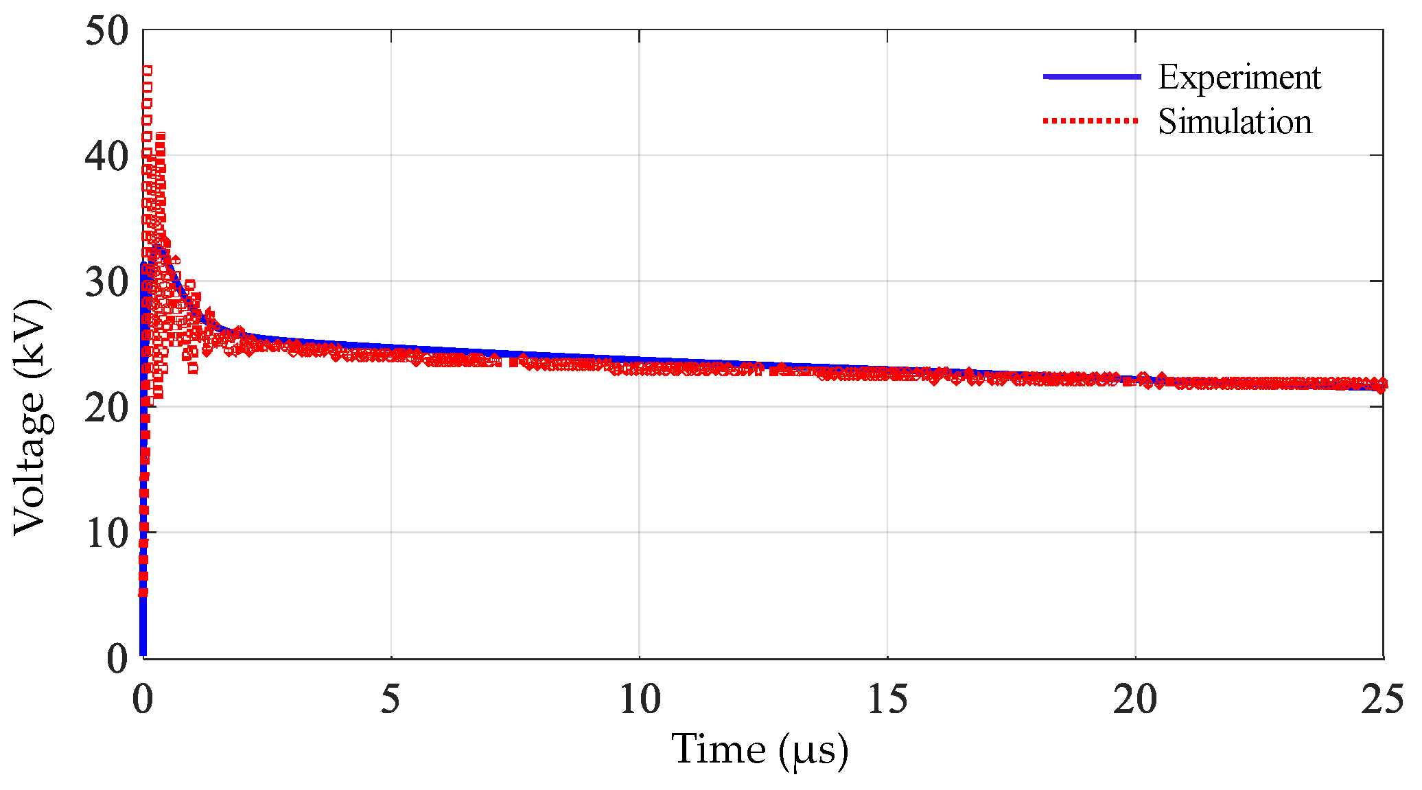
Section 4, those circuit parameters of the model were determined by matching the residual voltage from simulation with that from the experiment. As shown in
Figure 3 and
Figure 4, the calculated current waveform agreed well with the experimental result. The calculated peak voltage deviated from the experimental one by only 2%. However, the calculated residual voltage deviated from the experimental one. It was found that the calculated time to the peak of the residual was longer that the experimental one, and the spurious oscillation of the calculated residual voltage occurred in the late time or in the non-conductive state of the arrester.
3. Simplified and Accurate Model of a Surge Arrester
In the results presented in
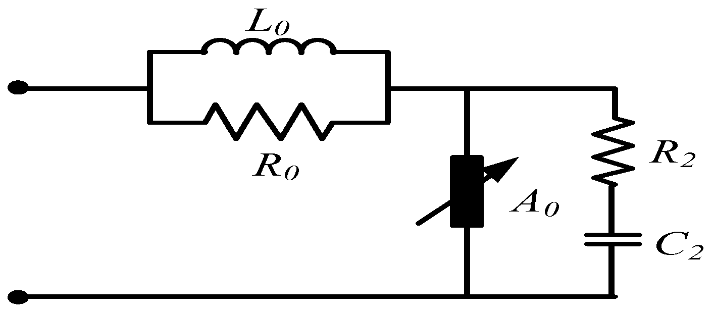
Section 2, the conventional arrester model provided inaccurate results when they were compared to the experimental ones. In this section, a simplified and accurate model of a surge arrester as shown in
Figure 5 is proposed to overcome the problems of the conventional model. The circuit parameters of the model were composed of the internal resistor (
R0) in parallel with the internal inductor (
L0), the nonlinear resistor (
A0), and the damping resistor (
R2) in series with the internal capacitor (
C2).
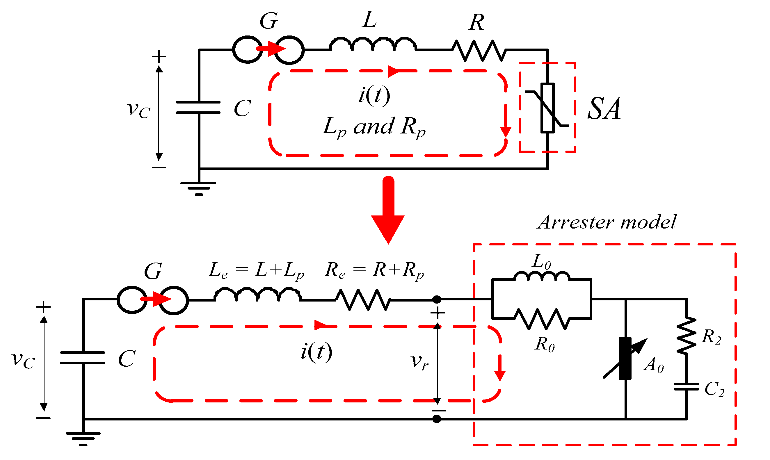
As mentioned above, the generation circuit, the parasitic impedance, i.e., series inductance (
Lp) and series resistance (
Rp), and the nonlinear characteristic of a surge arrester must be taken into account in the real impulse current generation. The simplified equivalent circuit including the parasitic impedance and the proposed arrester model is illustrated in
Figure 6. In real practice, it is possible to measure the charging capacitance, the charging voltage (
Vch), and the arrester capacitance precisely, but it is quite hard to measure other circuit parameters. However, the characteristic of the nonlinear resistor (
A0) can be approximated from the experimental results of voltage and current across the arrester. As shown in
Figure 7, in this paper, a piecewise linear curve drawn through the center of the data of voltage and current of the arrester was employed to represent the characteristic of the nonlinear resistor. A genetic algorithm was employed to search the unknown circuit parameters of the generation circuit and of the arrester model to match residual voltage (
vr) waveforms from the experiment.
4. Genetic Algorithm
A genetic algorithm (GA) is inspired by the process of natural selection. The genetic algorithm is a kind of stochastic optimization. In this paper, the genetic algorithm [
16,
17] was utilized to search the appropriate circuit parameters, i.e., the equivalent inductance (
Le), the equivalent resistance (
Re), the internal arrester inductance (
L0), the internal arrester resistance (
R0), the damping resistance (
R2), and the charging voltage (
Vch). The genetic algorithm searches the input parameters (the circuit parameter in the vector form;
X) to minimize objective function (
Ob(
X)), as given in Equation (1).
where
vr(exp) and
vr(sim) are the residual voltages from experiment and simulation using the arrester model.
i is the
ith residual voltage point and
n is a number of points of the measured and simulated residual voltages.
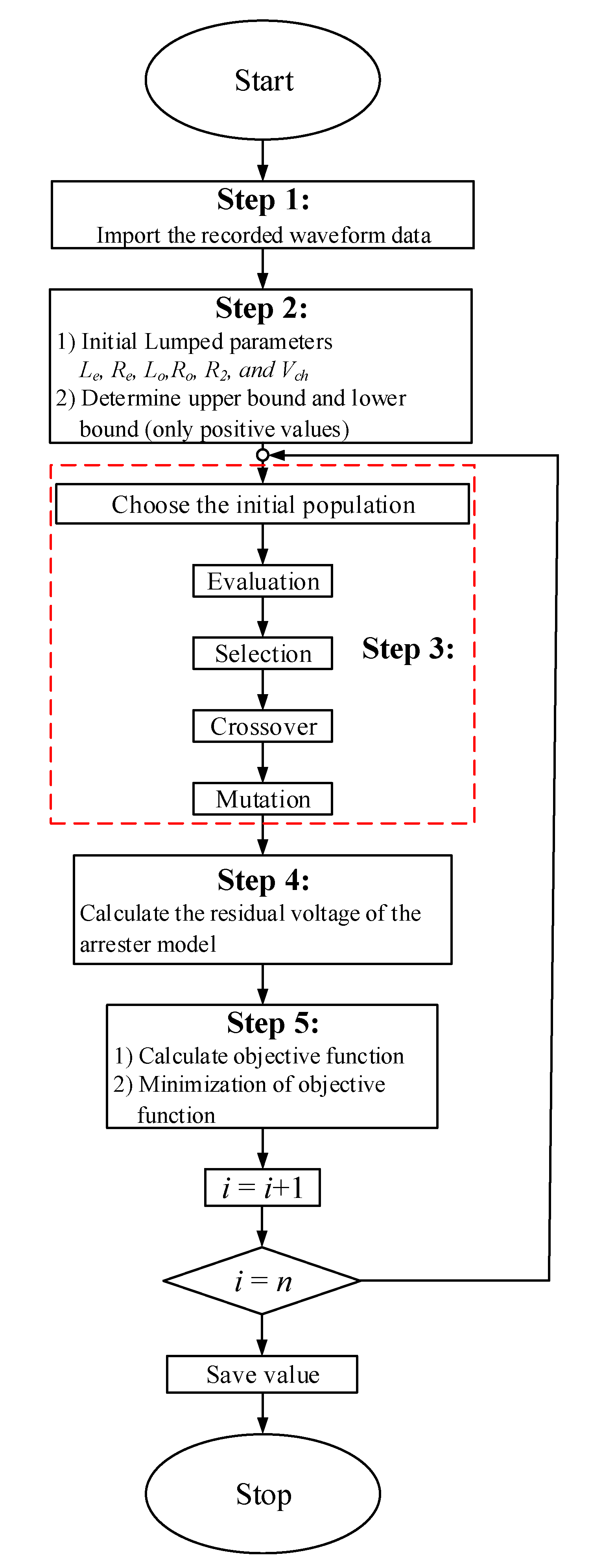
The flow chart based on the genetic algorithm for searching the most proper circuit parameters is presented in
Figure 8.
6. Applications of the Proposed Method in the Residual Voltage Test
It is hard for a test engineer to control the current waveform and peak without a trial and error approach. Therefore, in this section, an effective technique is proposed to determine the charging voltage for obtaining the current waveform according to the standard requirement. The technique starts from the determination of the unknown circuit parameters of the generation circuit and the proposed arrester model as shown in
Figure 6. The current and residual voltage waveforms from the preliminary test with the lower current peak specified by the standard were utilized to determine the circuit parameters. Then, the previous determined model and a genetic algorithm were employed to search the charging voltage to obtain the specified current peak.
To confirm the validity of the proposed technique, some experiments on the residual voltage tests were carried out on two surge arresters with the rated voltage of 9 kV. The first arrester had the nominal discharge current of 5 kA and the second one had the nominal discharge current of 2.5 kA.
According to the standard requirement [
3] for the residual voltage test of the lightning impulse current, 0.5, 1.0, and 2.0 times the nominal discharge current are generated through the arrester and the residual voltages are examined. In the preliminary experiment, the charging capacitance and voltage were set to be 2 µF and 30 kV, respectively, and the measured internal capacitance was 56 pF. From the known circuit parameters and to obtain the lightning impulse current waveform [
18,
19], the total inductance of about 30 µH was required, so the series inductor (
L) with inductance of 30 µH was connected to the generation circuit. As shown in
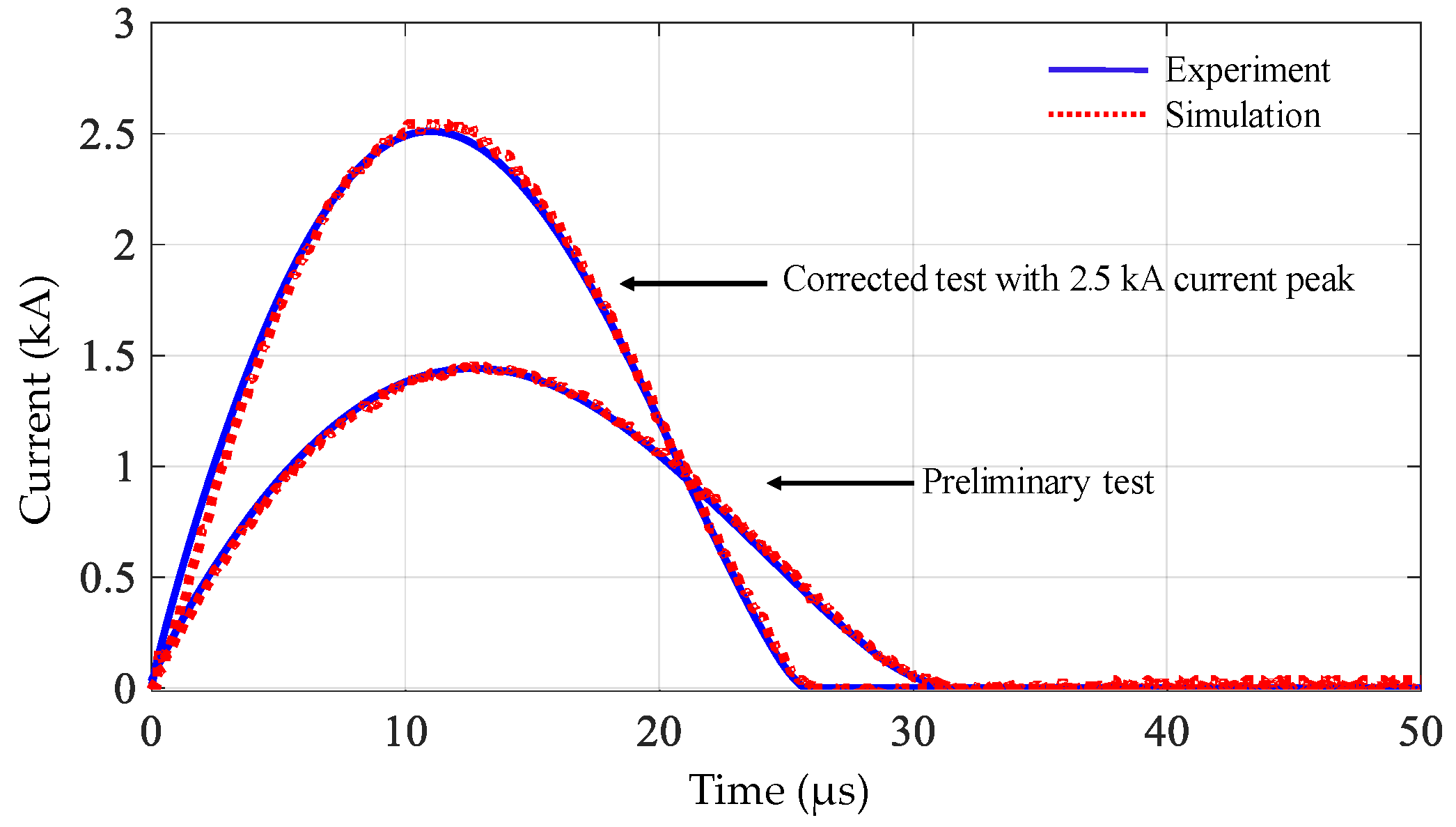
Figure 13, the current waveform deviated from the standard requirement due to effects of the parasitic impedance and the arrester. From the experimental results of current and residual voltage waveforms as shown in
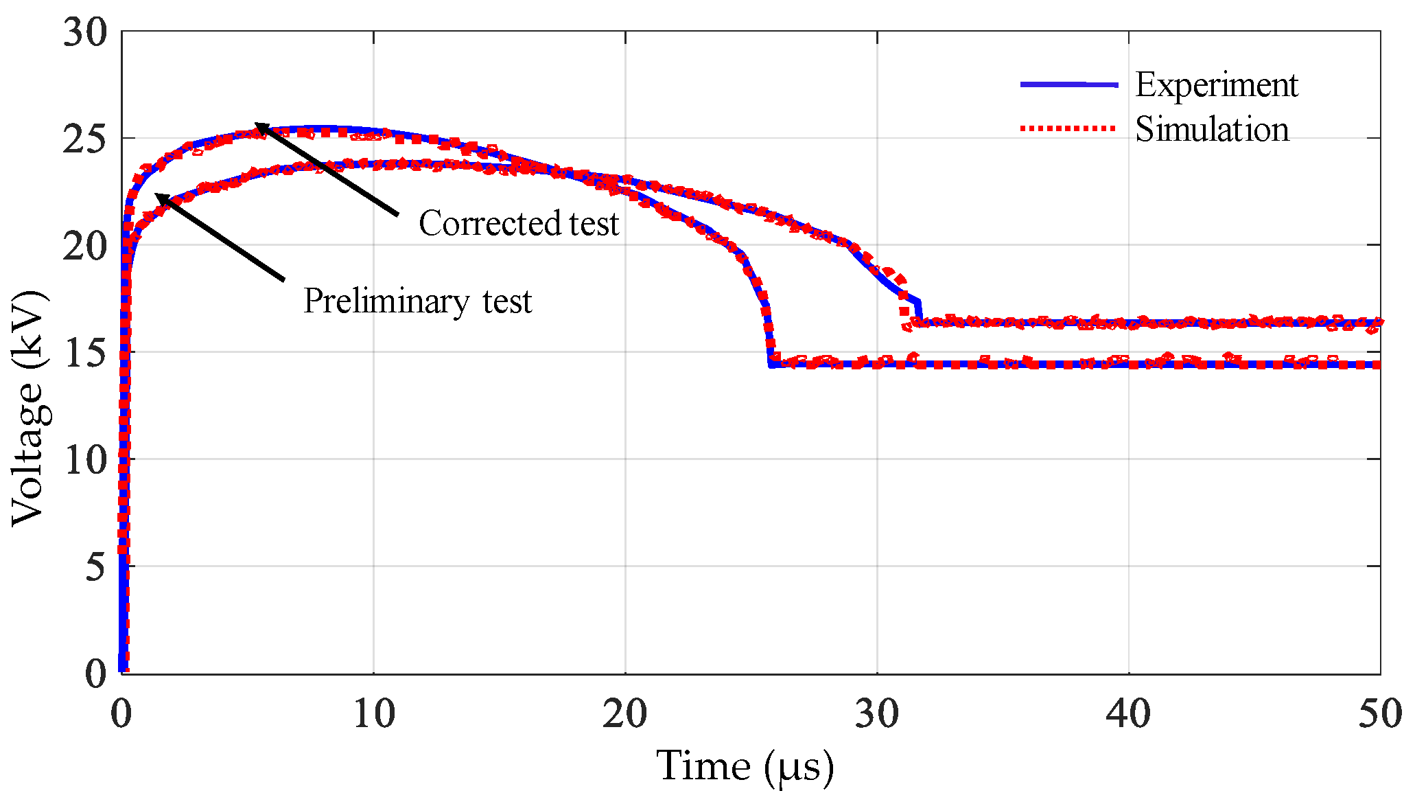
Figure 13 and
Figure 14, the circuit parameters were determined by using the equivalent circuit in
Figure 6. The equivalent inductance (
Le), the equivalent resistance (
Re), the internal arrester inductance (
L0), the internal arrester resistance (
R0), and the damping resistance (
R2) were 41.2 µH, 0.1 Ω, 4.1 µH, and 3.7 kΩ, respectively. From the determined circuit parameters, the total inductance in the circuit was 45.3 µH (
Le +
L0). Therefore, the series additional inductance of 14.7 µH was required to obtain the lightning impulse current waveform specified by the standard. Another experiment with an additional inductance of 15 µH was carried out to confirm the validity of the proposed technique. Furthermore, using the proposed technique, the calculated charging voltage of 34 kV associating with the current peak of 2.5 kA was set in the experiment. It was found that as shown in
Figure 13, the current waveform according to the standard specification was generated when the corrected circuit parameter was applied in the generation circuit. Moreover, the calculated residual voltage agreed well with that from the experiment as shown in
Figure 14. The time to peak of the calculated residual voltage was almost the same as the experimental one. The calculated peak current and voltage deviated from the experimental ones by only 0.55% and 0.35%, respectively.
In a similar manner, the proposed technique with the equivalent circuit associated with the current peak of 2.5 kA was applied to search the appropriate charging voltages associated with the current peaks of 5 kA and 10 kA. The piecewise linear curve used to estimate the nonlinear characteristic of the nonlinear resistor (
A0) is illustrated in
Figure 15. From the proposed technique, the equivalent inductance (
Le), the equivalent resistance (
Re), the internal arrester inductance (
L0), the internal arrester resistance (
R0), and the damping resistance (
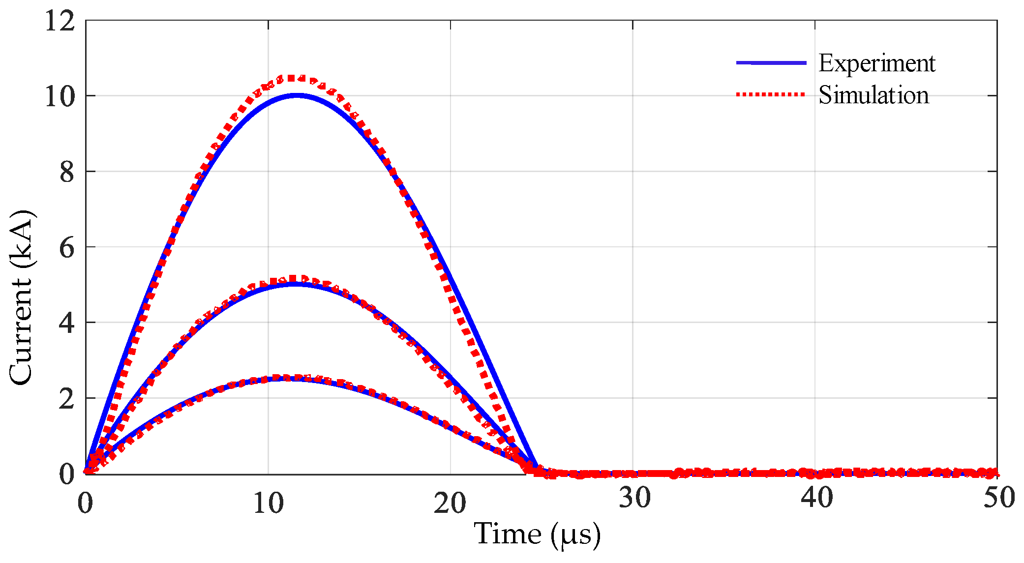
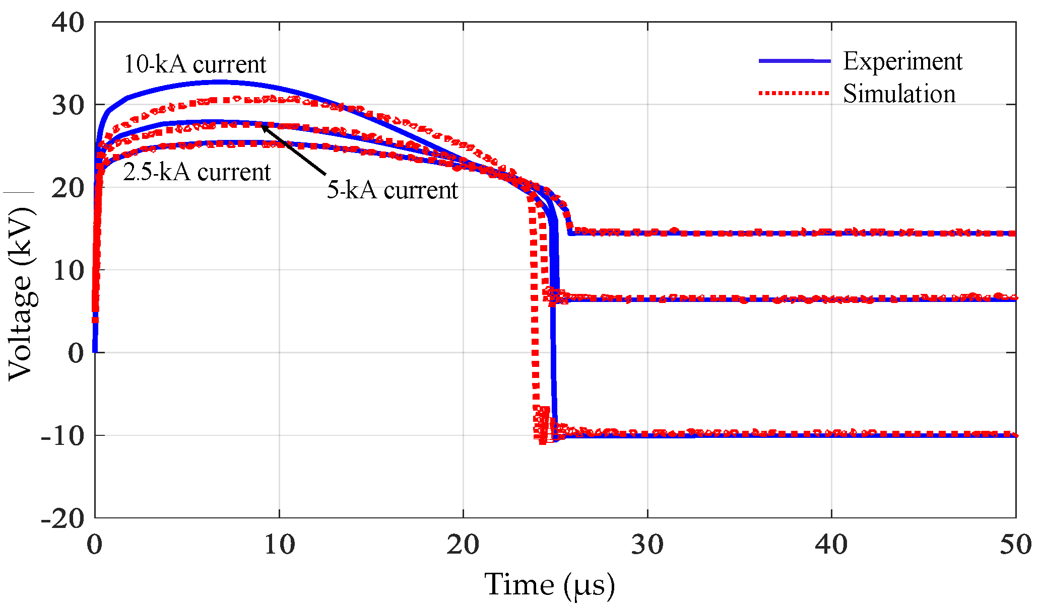
R2) were 27.1 µH, 0.1 Ω, 4.0 µH, and 3.6 kΩ, respectively. The charging voltages to obtain the current peaks of 5 kA and 10 kA were 46 kV and 69 kV, respectively. Comparisons of the experiment and simulated waveforms by the proposed technique are shown in
Figure 16 and
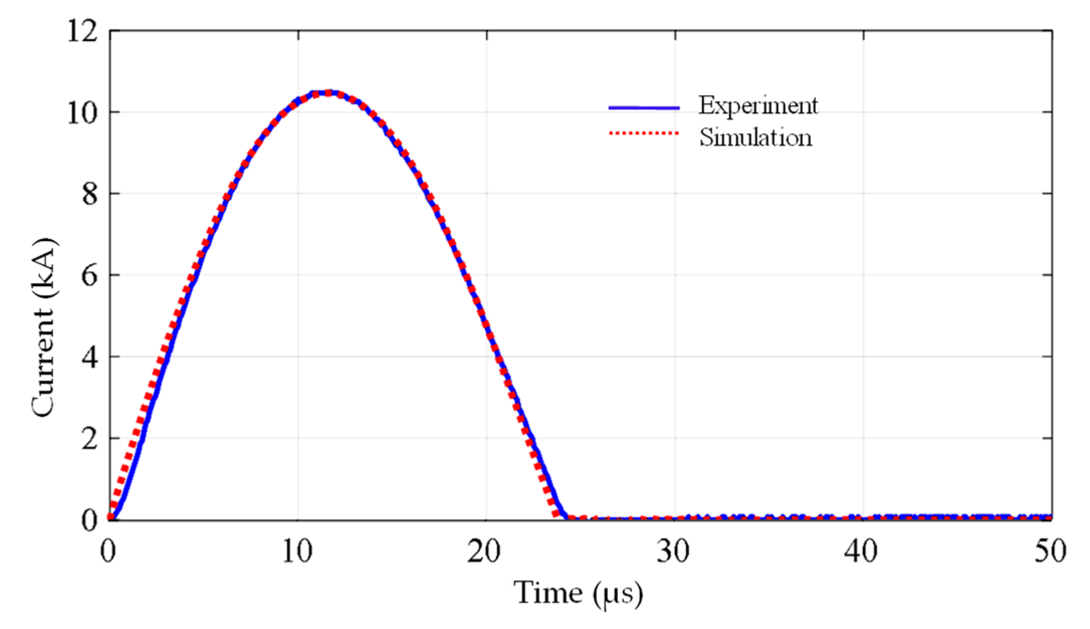
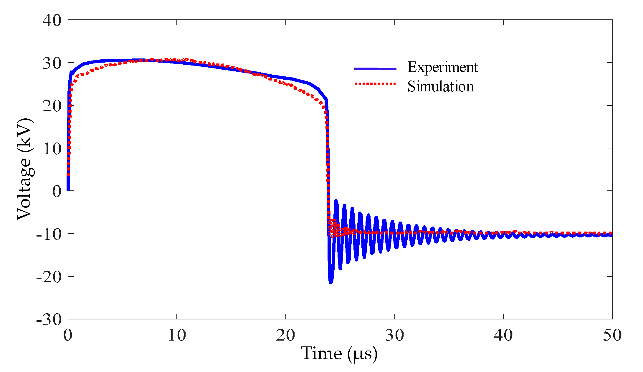
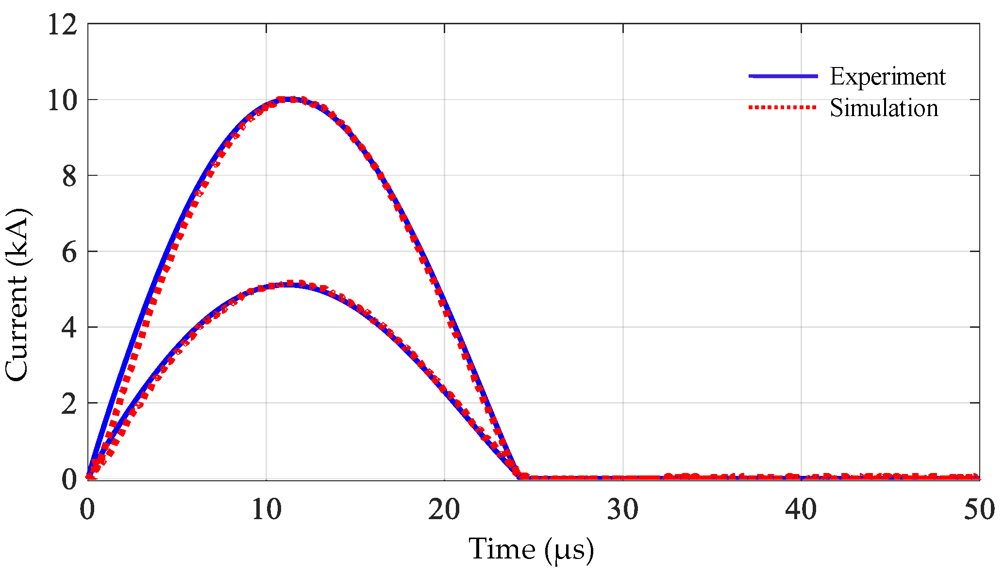
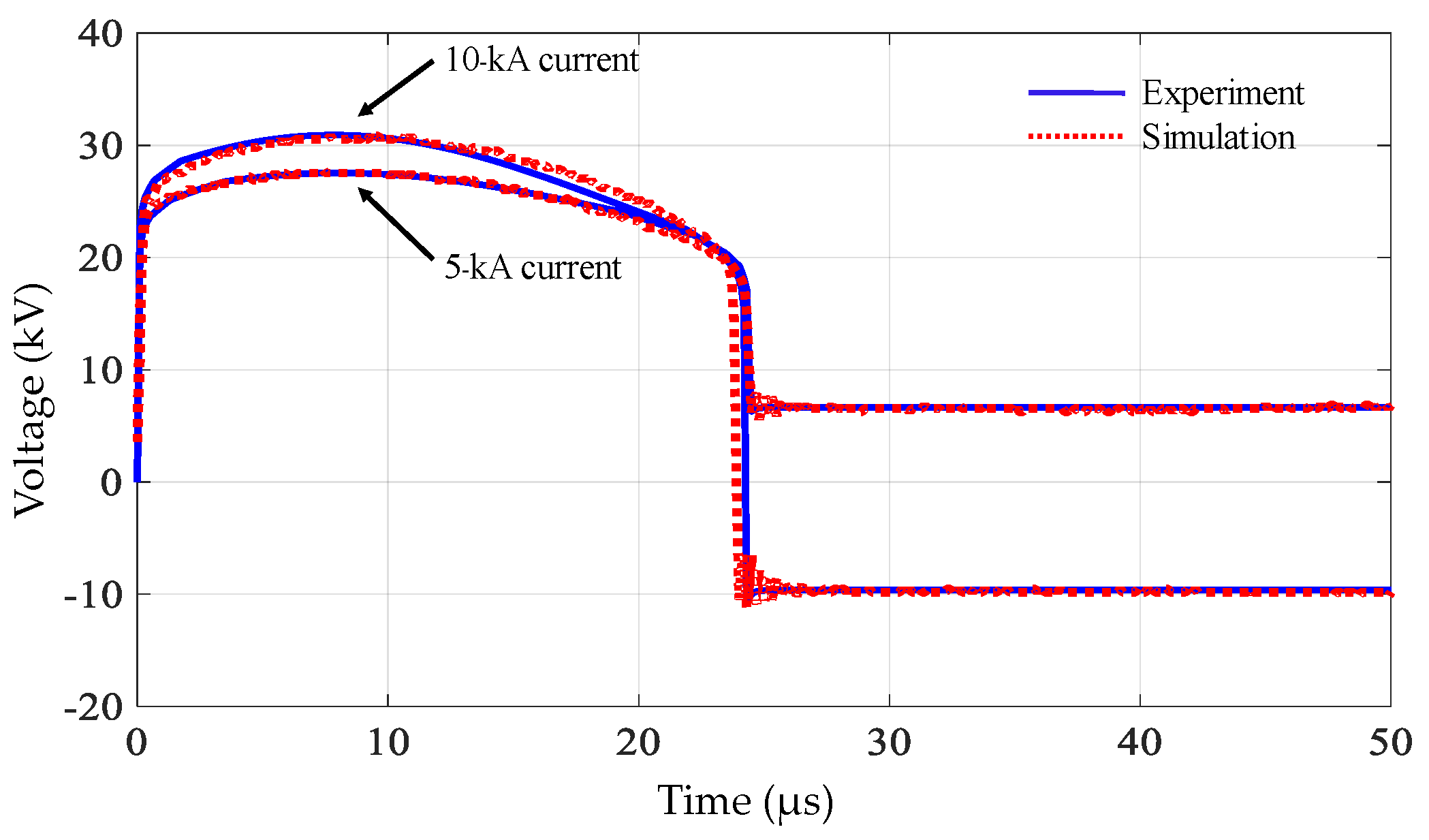
Figure 17. Good agreement was found in the case of 5 kA current peak but deviation occurred in the case of 10 kA current peak. In the case of 5 kA current application, the calculated peak current and voltage deviated from the experimental ones by only 0.73% and 0.88%, respectively. In the case of 10 kA current application, the calculated peak current and voltage deviated from the experimental ones by 4.1% and 8.1%, respectively. However, in terms of current generation in the case of 10 kA current peak, the deviation is acceptable because the current peak deviation of 4.1% was less than 10% according to the standard tolerance.
To obtain higher accuracy in the generation of the 10 kA current peak, the proposed technique was applied to model the equivalent circuit using the waveforms in the case of the 5 kA current peak and it was employed to determine the charging voltage to obtain the current peak of 10 kA. From the experimental results of current and residual voltage waveforms as shown in
Figure 15 and
Figure 16, the circuit parameters were determined by using the equivalent circuit in
Figure 6. The equivalent inductance (
Le), the equivalent resistance (
Re), the internal arrester inductance (
L0), the internal arrester resistance (
R0), and the damping resistance (
R2) were 26.9 µH, 0.1 Ω, 2.4 µH, and 3.1 kΩ, respectively. Using the model of the 5 kA current peak, the calculated charging voltage to obtain the current peak of 10 kA was 67.3 kV and a charging voltage of 67.5 was set in the experiment. Comparison of the generated currents by simulation with the proposed model and that from the experiment is shown in
Figure 18. In addition, the comparison of the experimental and simulated residual voltages is shown in
Figure 19. A better agreement between the simulated and experimental was found. The calculated peak current and voltage deviated from the experimental ones by only 0.43% and 0.56%, respectively.
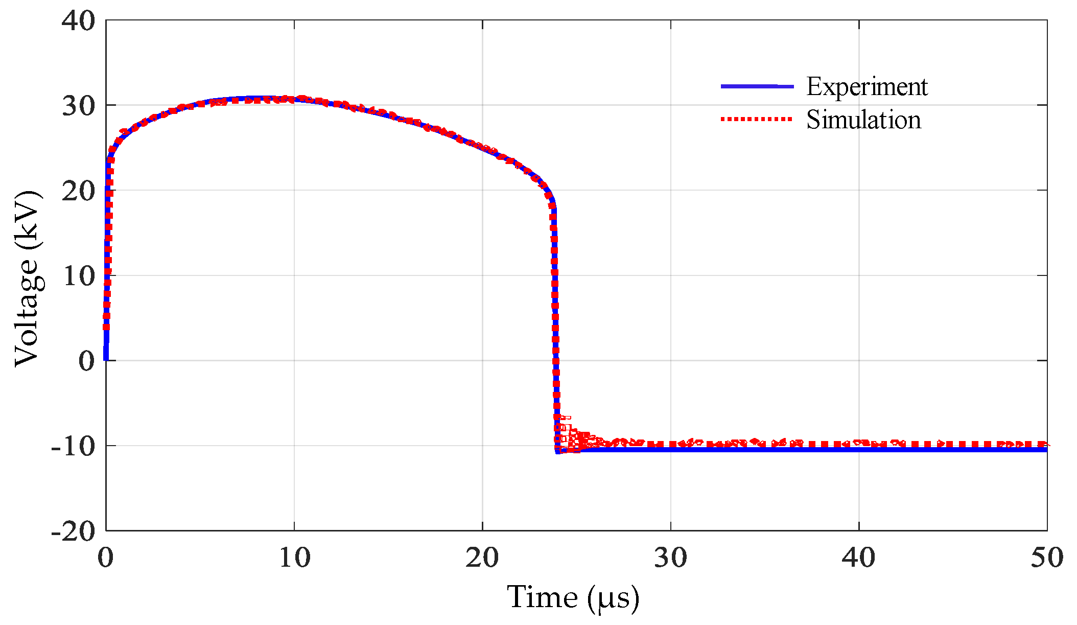
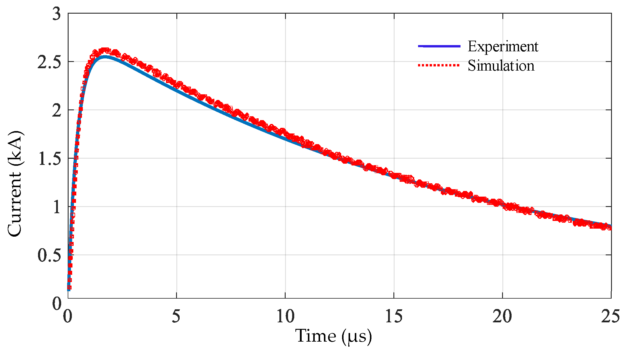
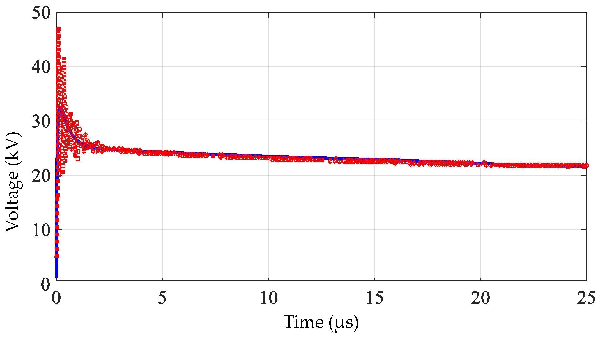
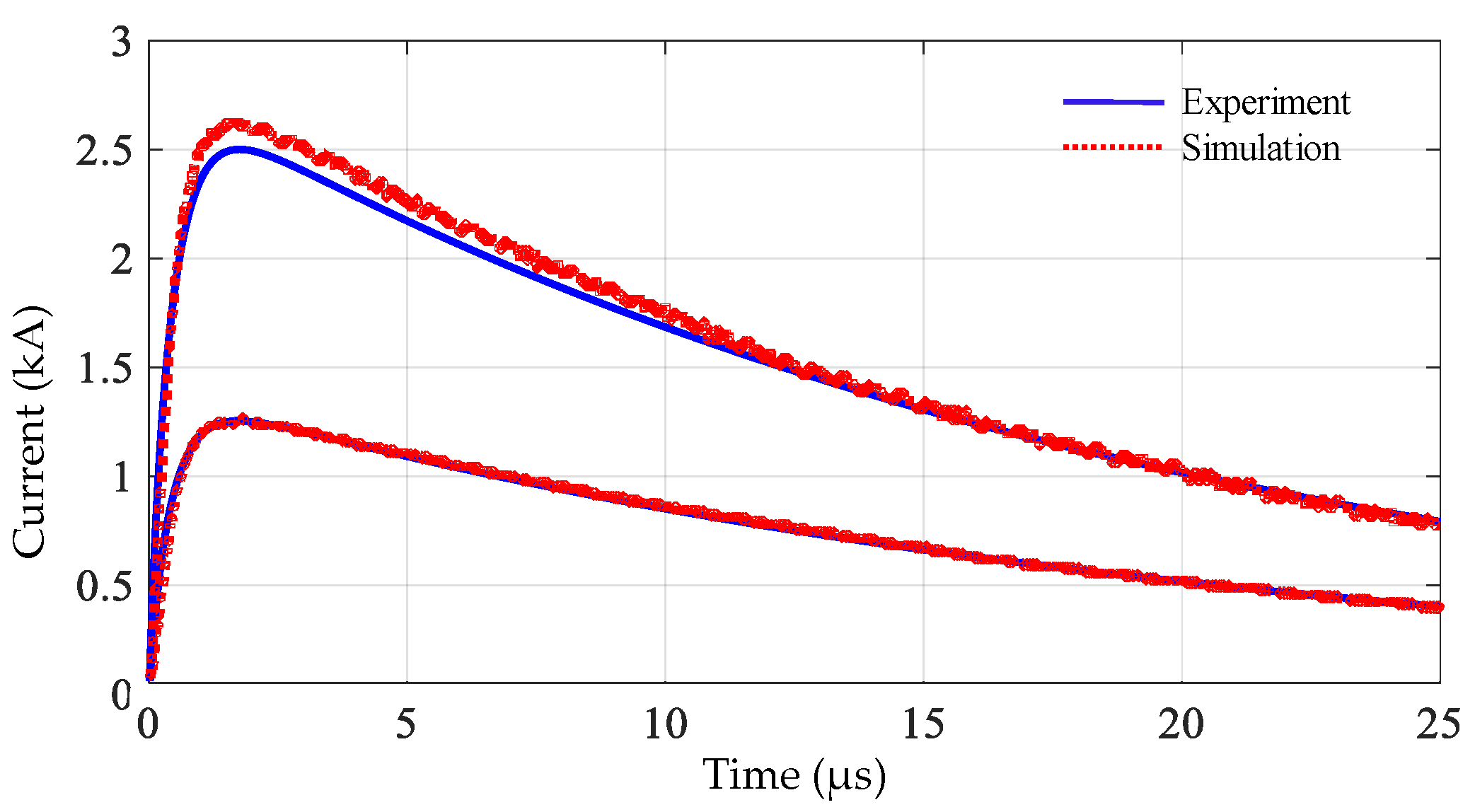
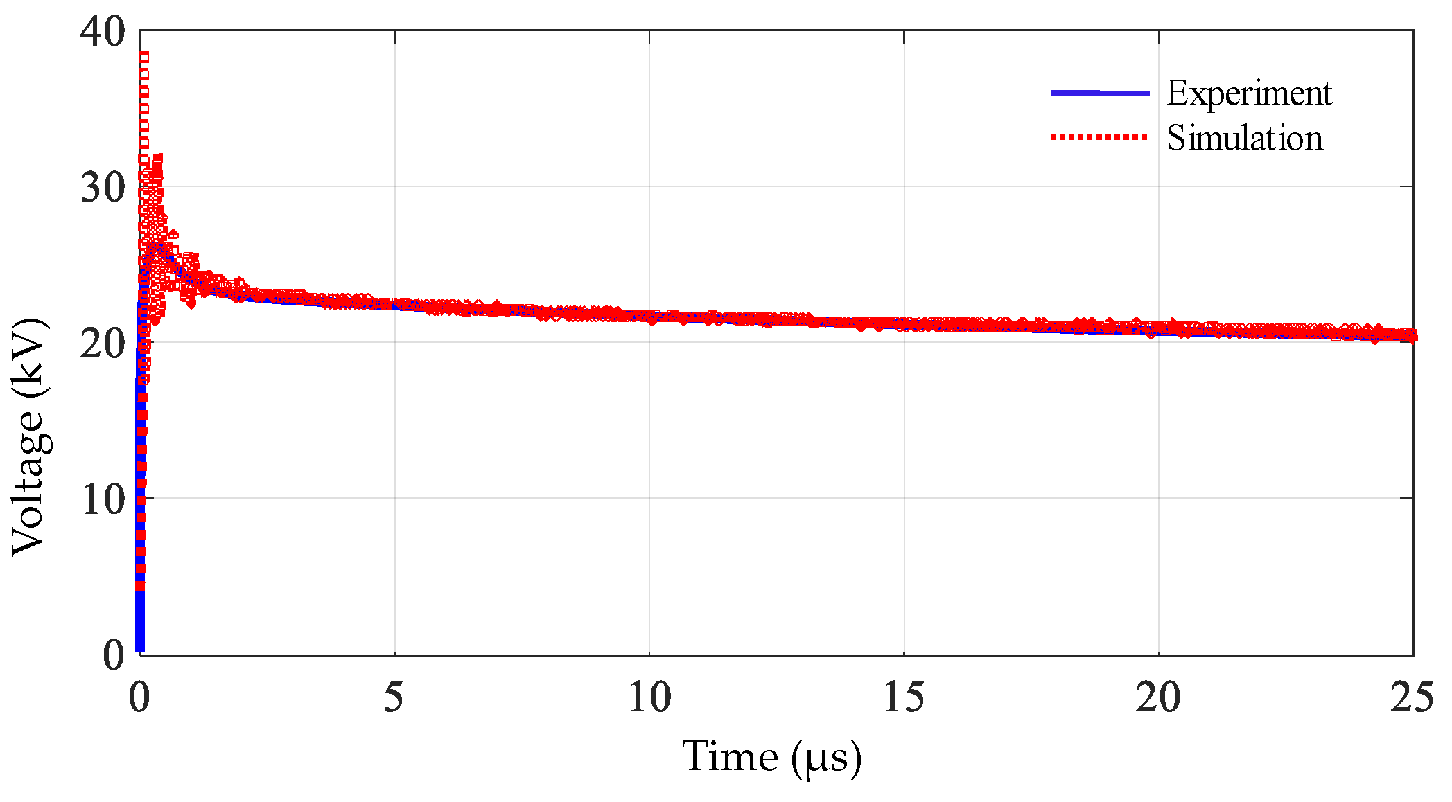
In a similar manner, the proposed technique was applied for the residual voltage test on the arrester with the nominal discharge current of 2.5 kA. The preliminary test with a steep impulse current was carried out at the current peak of 1.25 kA. For the steep impulse current generation, the charging capacitance, the charging voltage, and the additional resistance were set to 2 µF, 78 kV, and 38 Ω, respectively, and the measured internal capacitance was 50 pF. From the calculation using the proposed technique, the equivalent inductance (
Le), the equivalent resistance (
Re), the internal arrester inductance (
L0), the internal arrester resistance (
R0), and the damping resistance (
R2) were 14 µH, 0.1 Ω, 2.8 µH, and 198 Ω, respectively. Using the proposed technique to obtain the current peak of 2.5 kA, the calculated charging voltages was 134.5 kV and the setting charging voltage in the experiment to confirm the validity of the proposed technique was 135 kV. Comparisons of the experiment and simulated waveforms by the proposed technique are shown in
Figure 20,
Figure 21 and
Figure 22, in which good agreement is found. It was confirmed that the proposed technique is very effective in the residual voltage tests. In the case of 2.5 kA current application, the calculated peak current deviated from the experimental one by 7.8%, which is still in the standard tolerance.


