1. Introduction
Vertically stacked 3D integrated circuits [
1,
2,
3] have many important advantages, like smaller footprint, lower delay, higher operating speed, potentially higher yield, combining different technologies on a single die, etc. With the first 3D memory chips already on the market, it seems inevitable that this trend will continue, and soon the first processors with multiple silicon layers will be produced. While going 3D is certainly a major step towards maintaining Moore’s Law, there are still many challenges which need to be addressed. Most importantly, the technology of vertical interconnections using through-silicon vias (TSV) has to be mastered. Recent breakthroughs in this field [
4,
5,
6,
7] indicate that chip manufacturers are close to achieving this goal. The bonding technology and mechanical stability is another crucial issue [
8,
9].
From a thermal perspective, 3D stacking poses significant challenges due to quite obvious reasons: each stacked layer increases the power dissipated in almost the same area. As a consequence, the power density and the resulting temperatures increase rapidly as more and more layers are stacked. Another issue is the difficulty of removing heat from the bottom layers. In a conventional cooling system, most heat is dissipated to ambient through the heat spreader and heat sink, which are put on the top layer. In a 3D chip, as the layers are usually bonded with a material with very low thermal conductivity (typically around several W/(mK)), the vertical thermal resistance between the layers is high (compared to the thermal resistance of the silicon layer itself). With multiple layers present, this results in a very high thermal resistance between the bottom layer and the heat sink and, therefore, higher peak temperatures are produced.
To tackle these two problems, integrated microchannel cooling [
10,
11] has been suggested. In fact, it was even considered before as a potential cooling solution for 2D chips, but this particular idea is especially promising when considering 3D ICs. The reason is that it perfectly addresses the two issues mentioned in the previous paragraph. First, liquid cooling offers much higher cooling performance: it is estimated that the heat transfer coefficient may be several orders of magnitude higher than in the case of the classic approach based on forced air convection [
12]. Second, if microchannels are implemented in all chip layers, the problem of high vertical thermal resistance is eliminated, and the heat is removed almost equally from all chip layers. In other words, the performance of microchannel cooling is scalable: stacking more layers increases power density, but also proportionally increases cooling, so the resulting peak temperature should remain almost the same.
The most valuable research on microchannel cooling is based on real measurements using specially designed test chips [
13,
14]. However, often, measurements of 3D ICs with liquid cooling are not possible for various reasons. Sometimes, the manufacturing technology is not yet available, or the costs may be too high. Therefore, researchers use simulations as a means to estimate the influence of chip and cooling parameters on chip temperatures. The most commonly used approach is based on the finite element method (FEM), using commercial CFD tools like Ansys [
15], Comsol [
16] or FloTherm [
17]. The main advantage of this method is its relatively high accuracy [
18,
19]. However, this approach uses a coupled thermo-fluidic simulation and, as modelling fluid dynamics requires a very fine mesh, the resulting number of model nodes is very high (hundreds of thousands) and simulation times are very long [
20,
21]. In an attempt to shorten the simulation time, many authors have suggested simpler models. In [
22], a compact thermal modelling tool 3D-ICE for 3D ICs with microchannels was proposed. By comparing its results with measurements, it was shown that the average error introduced by the model is below 10%. In [
23], the authors suggested using a time-variant resistor model to describe the convective heat transfer in heated microchannels. The authors validated their model against Ansys Fluent and obtained an error of 5%. The authors of [
24] developed an algorithm allowing the simulation of microchannel-cooled 3D ICs on GPUs. These authors reported errors below 0.5 °C with respect to the traditional CPU-based approach while also achieving considerable speedup with their method. The model based on thermal wake function was introduced in [
25]. Numerical pre-simulation was used to extract the function and build a thermal wake aware resistance network model. The authors compared their model with a commercial CFD tool and reported an error of less than 2.0% and a 400× speedup. In [
26], the authors extended the existing compact thermal simulator with an equivalent 3D resistive network to model liquid cooling. The model was then used to validate a dynamic thermal management scheme, which allowed up to 95% reduction in hotspots on average. The authors of [
27] describe an analytically derived T-equivalent analytical thermal model of a microchannel. Validation of the proposed approach was based on the simulation of one channel in SPICE. Authors reported a good agreement of their model (errors below 2%) with the results obtained with a full CFD simulation.
This paper demonstrates the advantages of TIMiTIC—a compact thermal simulator for chips with liquid cooling—and shows its practical usefulness in design space exploration of 3D ICs with integrated microchannels. In comparison with other approaches, more focus is given on the modelling of convection resistance between the solid and the fluid, especially the thermal entry effects and the variation of the Nusselt number along the channel. The accuracy of the simulator was already analyzed in [
28], where its results were extensively compared with the ones obtained using CFD simulation in Comsol. The validation with respect to full CFD simulation showed a very good agreement (the average absolute error of 1.3 °C and the average relative error of 3.7% for the worst analyzed case).
Moreover, thermal simulations of a 3D processor model using the proposed tool are used to estimate the optimal power dissipation profile in the chip and to prove that such an optimal profile allows for a very significant (more than 10 °C) peak temperature reduction. Finally, a custom correlation metric is proposed which allows comparing the power distribution profiles in terms of the peak temperature that they produce. Statistical analysis of the simulation results demonstrates that this metric is very accurate and can be used, for example, in task scheduling or dynamic voltage and frequency scaling (DVFS) algorithms.
2. Characteristics of Microchannel Cooling
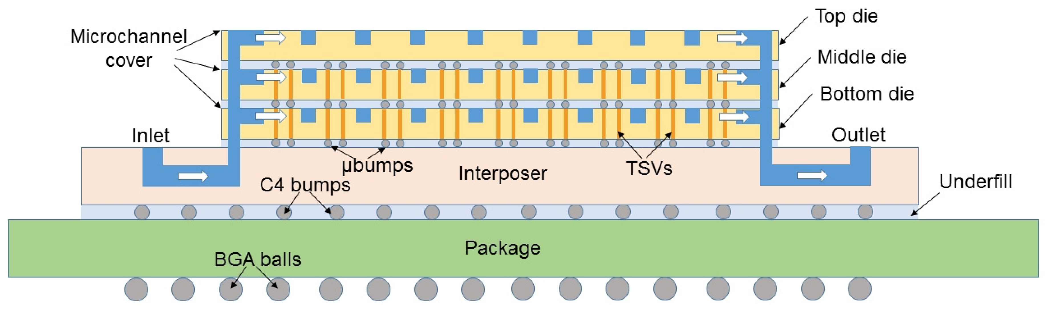
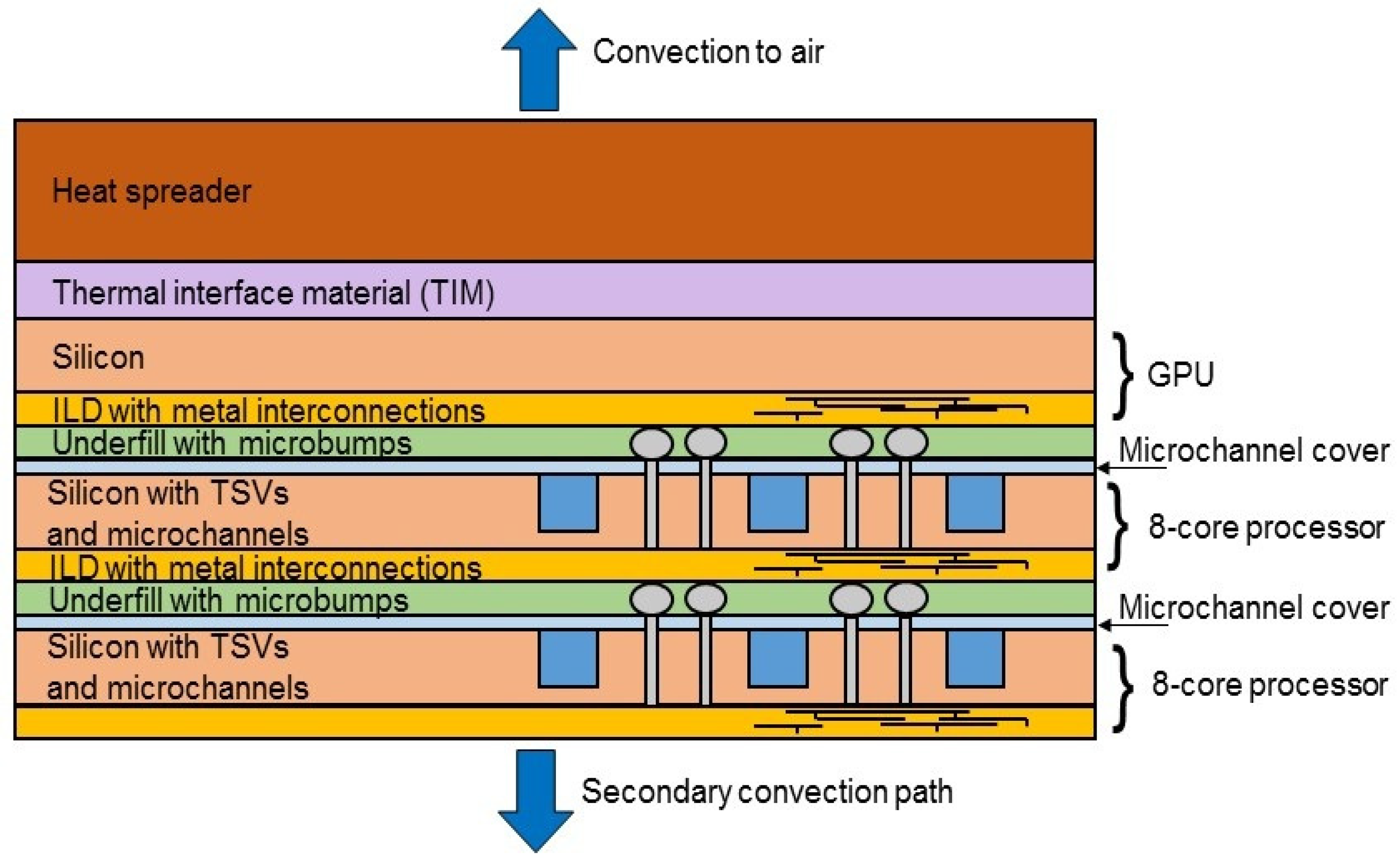
A sample 3D chip with microchannels etched in each silicon layer is shown in
Figure 1. The inlets/outlets to the chip can be implemented as tubes connected on top of the chip [
29] or as channels in the interposer (see
Figure 1). Then, the liquid is distributed among the layers using microchannels. The exact description of the manufacturing process of such liquid-cooled chips is beyond the scope of this paper. However, understanding how the heat is removed in such a liquid cooling system is crucial, therefore it will be described in detail.
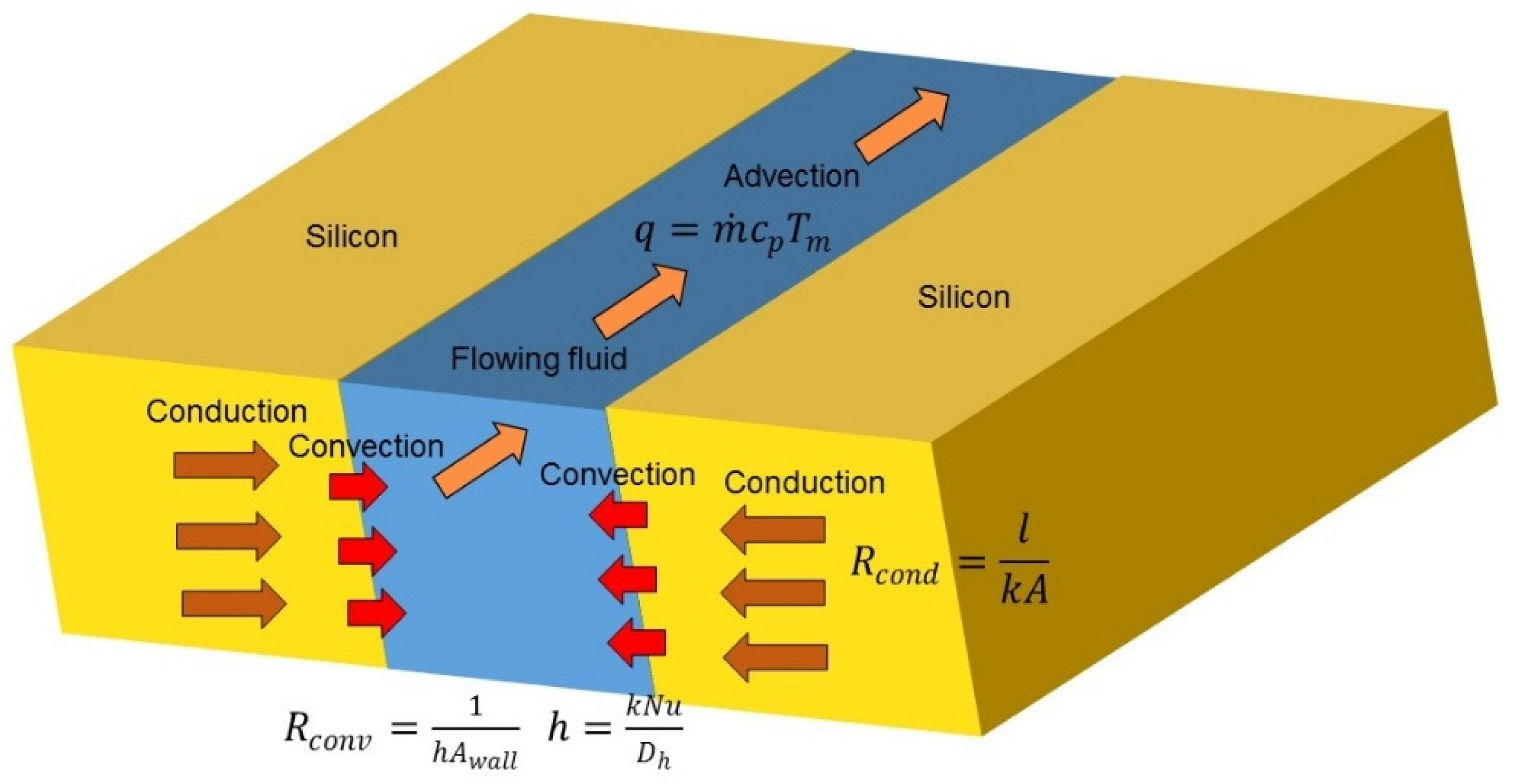
Figure 2 shows the three phases of heat removal. In the first phase, the heat generated in the active layer of silicon travels to the border of the microchannel by means of conduction (1). The conduction thermal resistance is inversely proportional to the thermal conductivity of silicon
k and is comparably low. In the second phase, the heat from the solid is absorbed by the fluid by means of convection. The thermal resistance across the solid–fluid border is inversely proportional to the channel surface area
Awall and to the heat transfer coefficient (HTC)
h, see (1). It is worth emphasizing that the HTC is not constant: in fact, it is proportional to the Nusselt number
Nu, which decreases significantly from the channel inlet to channel outlet [
30,
31]. Therefore, the convection thermal resistance is always higher at the inlet side of the chip and lower at the outlet side. In the third and final phase, the heat is transported by the fluid by means of advection (1). The important detail to notice is that the temperature of the flowing fluid is increased because of all the heat absorbed upstream.
where
l is the length of the solid block,
A is the cross-section of the solid block,
is the mass flow,
cP is the specific heat of the fluid,
Tm is the mean temperature of the fluid and
Dh is the hydraulic diameter of the channel.
Consequently, there are two mechanisms which cause gradually worse cooling performance as we move from inlets to outlets, one related to convection and one related to advection.
Thus, the thermal behavior of microchannel-cooled chips is significantly different than that of chips cooled by a heatsink and a fan. In a 3D chip with a conventional air-cooled system, the top chip layers will be cooled best, and the cooling performance will decrease for each layer farther from the heat sink. However, there is no intra-layer cooling performance variability, so all places located in the same layer are cooled almost equally. Meanwhile, in a 3D IC with microchannel-based system, there is no inter-layer cooling performance variability (all layers are cooled equally, provided that channels are implemented in all layers). However, within the same layer, the cooling performance varies: it is the highest near the inlets and the lowest at the outlets.
This leads to two important repercussions:
The floorplanning strategies which worked the best for chips cooled by forced air convection are not going to work well for IC cooled by microchannels.
The same applies for all thermal-aware task scheduling mechanisms and DVFS algorithms.
There have been a number of works which tackled the problem of thermal-aware floorplanning in 3D ICs and proposed algorithms to find the optimal floorplan for a given power distribution (power dissipation of every chip unit) [
32]. In this paper, this issue will not be analyzed. The reason is that chip floorplans (and especially high-end processors) are primarily optimized for performance (minimizing interconnect delay) and chip manufacturers are unlikely to change this based on the thermal performance. Therefore, in what follows, we will concentrate on demonstrating the usefulness of the proposed model for:
Thermal-aware task scheduling for multi-core processors, which aims at reducing the peak chip temperature by optimally distributing tasks among processor cores;
DVFS algorithms which minimize the peak temperature by appropriately changing the voltage and frequency of the cores.
3. TIMiTIC Simulator
The TIMiTIC tool was already extensively described in the previous paper [
28]; therefore, here, only its most unique and important aspects will be presented. In general, TIMiTIC follows a widely accepted approach to discretize the chip model into a large number of cells (or nodes). Using the equivalence between the thermal and electrical domain, each cell is then represented by a lumped-capacitance model. The resulting circuit can be then described with Equation (2).
where
G is the conductance matrix,
C is the capacitance matrix and
Q is the heat source matrix. This differential equation can be then solved using standard methods.
The first idea which differentiates TIMiTIC from other published compact models is the improved and flexible approach to convection modeling. While both conduction and advection are quite accurately described by their respective analytical descriptions (1), convection modeling is the weakest link in every compact thermal model. The reason is the dependence of the HTC on the Nusselt number (Nu), which varies depending on many factors:
The type of flow. The fluid flow can be both hydrodynamically and thermally developing or hydrodynamically developed and thermally developing; see [
30] for more detailed information.
Channel cross-sectional shape. Nu differs not only depending on the channel shape, but also varies for different aspect ratios for rectangular channels [
30].
The distance from the inlet. As already stated in the previous section, Nu decreases quickly from the inlet [
30] until the flow becomes thermally developed and Nu becomes constant. The exact shape of the curve Nu(x), which describes Nu in the entrance region depending on the distance from the inlet x, is difficult to estimate.
The boundary conditions. In the literature, Nu(x) is usually given for two very specific cases (UWF - uniform heat flux or UWT - uniform wall temperature). However, for any other boundary conditions, Nu(x) will be different. It is also worth noting that this Nu variation is quite high. Let us give the simplest example. For a developed flow in a circular channel, Nu equals 4.36 for the UWF boundary condition and 3.66 for the UWT boundary condition, which means that it changes by a factor of 1.19. Thus, significant error when modelling convection thermal resistance can be produced if it is not taken into consideration.
Therefore, it is very difficult to find a Nusselt number formula which would encompass all above-mentioned cases. Most models presented in the literature just use one Nu(x) formula and assume that it should work in all cases. However, it can be estimated that errors up to dozens of percent may be produced when following this approach. In TIMiTIC, the user can choose from many Nusselt number correlations described in literature [
33,
34], but, more importantly, he can specify his own correlation. In other words, when the user knows the flow type, channel dimensions and boundary conditions, he can easily implement in the simulator the Nusselt number correlation Nu(x) which most accurately describes his case.
Another important feature of the proposed tool is the use of well-established and thoroughly optimized mathematical libraries, like EigenSparseLU [
35] or odeint [
36], which allow for fast simulation. Especially in steady-state cases, TIMiTIC visibly outperforms FEM simulators, even by a factor of 100,000. The speedup is possible thanks to the use of the C++ language and the use of the solver dedicated to operate on sparse matrices. It was shown in [
28] that the simulation time which took 20 min in COMSOL produced almost the same results in just 10 milliseconds using TIMiTIC.
Moreover, as 3D ICs contain a large number of very thin layers, TIMiTIC allows reducing the simulation time by treating these layers as resistances and neglecting their thermal capacity. Thus, the number of nodes in the model can be greatly reduced, and the resulting error should be negligible because the thermal capacity of such thin layers is negligible compared to others.
Lastly, the TIMiTIC simulator is available for everyone to use through the Internet website [
37]. The user just has to prepare two files: the first file describes the 3D stack, material properties, channel parameters, etc., and the second file contains the power trace for all chip units. Using the website, the user can then upload these two files and run the simulation. There is no need to download or compile any code, the entire simulation takes place in a browser thanks to the use of Webassembly [
38] technology.
5. Results
5.1. Peak Temperature Variability Simulations
The simulations presented in this section have two goals: first, to demonstrate the usefulness of the simulator and, second, to prove that the appropriate DVFS algorithm or efficient scheduling of tasks to cores can reduce the maximum temperature by more than 10 °C in 3D ICs cooled by microchannels.
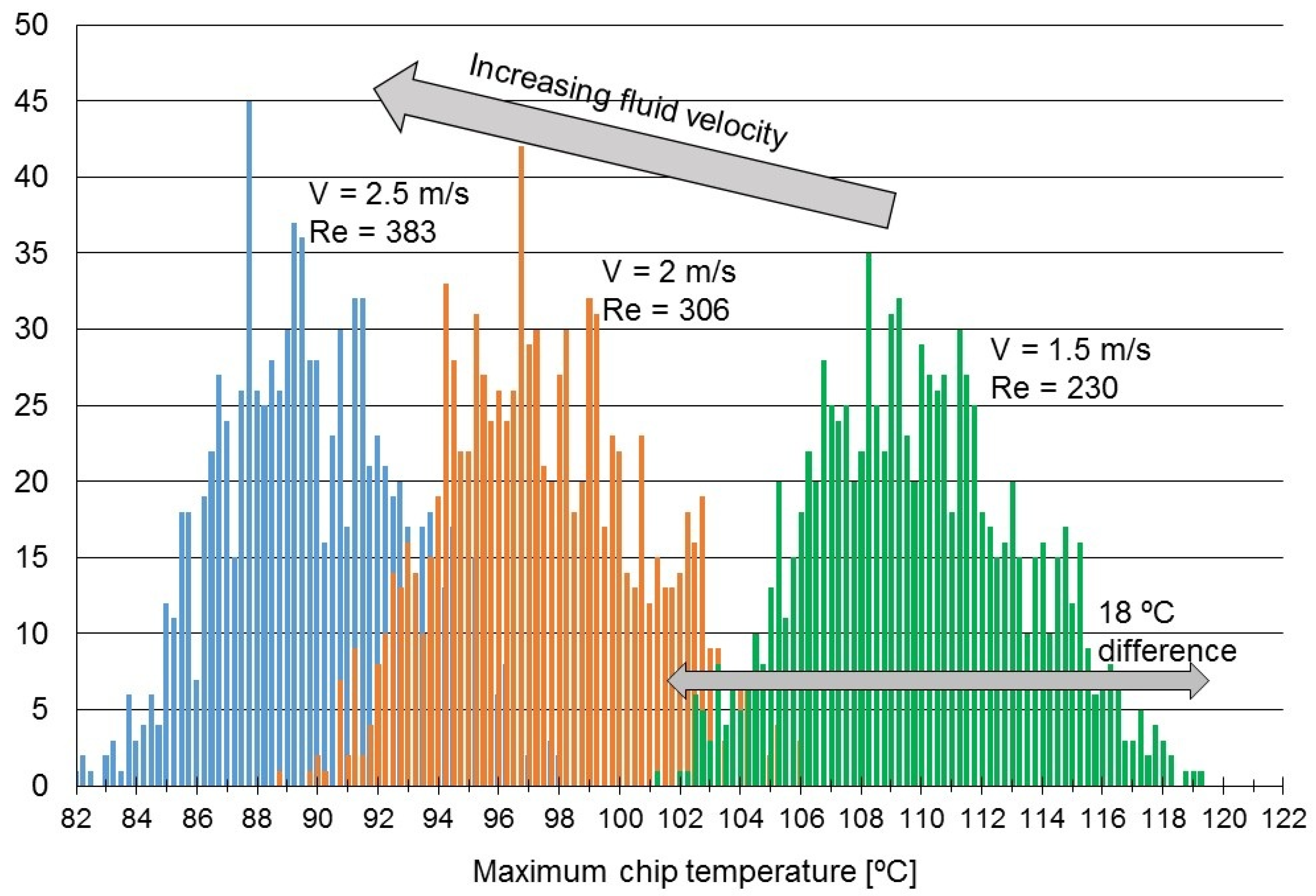
The methodology adopted in this section assumes that each core dissipates different power (for example, it can be seen as equivalent to cores executing different tasks, which vary in terms of how computationally intensive they are), but the total power dissipation is always constant. Therefore, 1000 power distributions were generated randomly assuming that the maximum power dissipated in a core can be equal to 13.5 W and the minimum to 4.5 W. Next, 1000 simulations were run using these power data (the default power distribution shown in
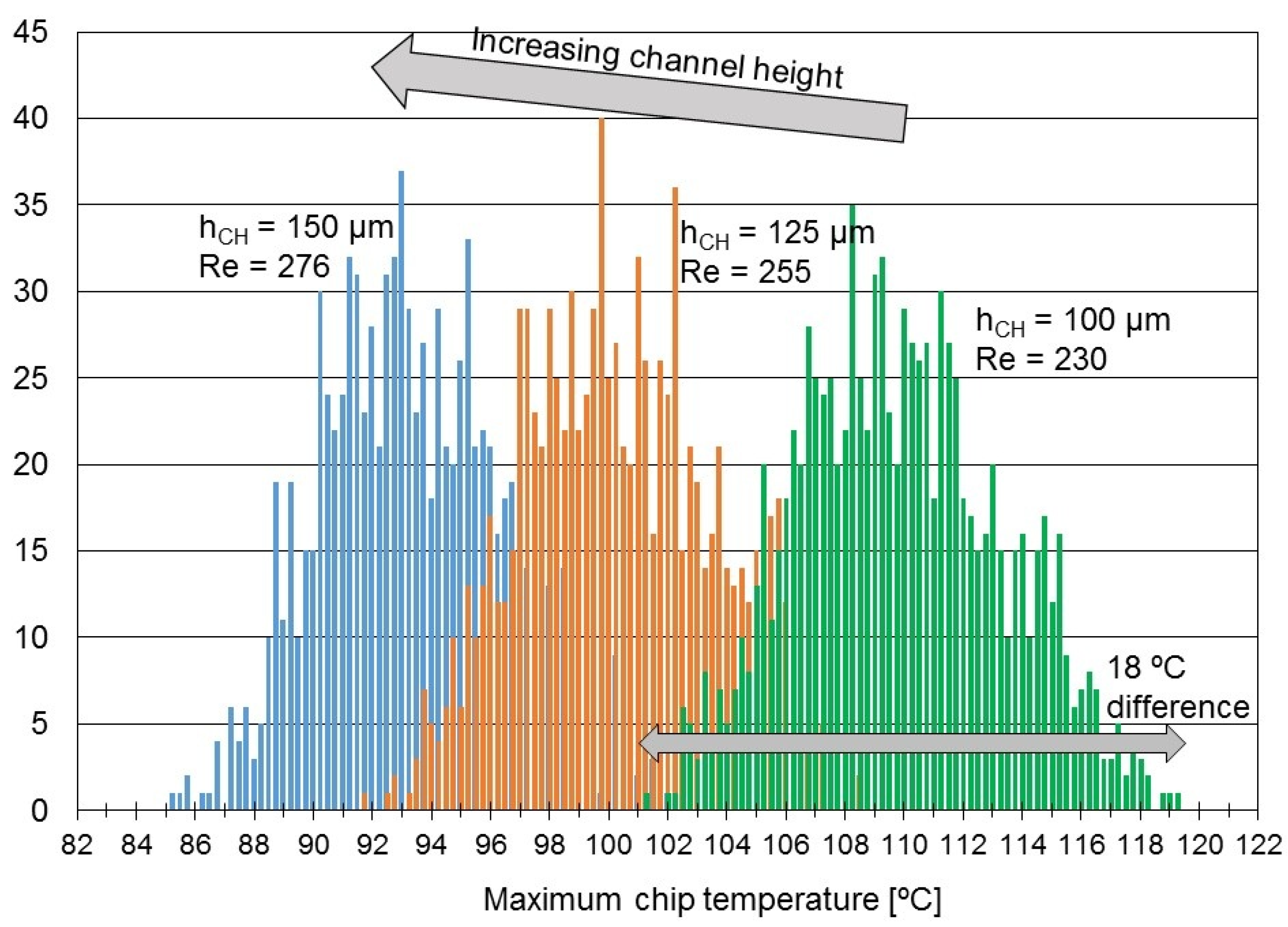
Table 1 was modified). Then, the distribution of maximum temperatures found in the chip for each case was reported. Note that running 1000 simulations using any FEM-based tool would not be feasible, as one simulation of such a chip can typically take up to several hours. With the TIMiTIC simulator, one simulation took only about two seconds, so the total simulation time needed for 1000 iterations was around 40 min. The same set of simulations was repeated for different values of fluid velocity (mass flow) and channel cross-sectional area. The results are presented in
Figure 6 and
Figure 7.
As expected, when increasing the fluid velocity, the temperatures decrease for two reasons: first, the advection thermal resistance is lower and, second, the thermal entry length is higher, which results in a higher average HTC between the solid and the fluid. Similarly, when increasing channel height, the convection resistance is decreased and temperatures goes down. These two observations are quite obvious, but other more interesting conclusions can be also drawn.
The obtained results resemble a normal distribution. The distribution shape varies only slightly when the fluid velocity or the channel height are changed, which indicates that, regardless of the parameters of the cooling system, the difference in maximum and minimum temperatures for different power distributions remain almost constant. In other words, we can conclude that peak temperature variability is independent of the cooling system.
It is important to emphasize that the power values were the same in all 1000 cases; just power-to-core-mapping was changed. This leads us to an important observation: the peak temperature variability has to be a direct result of the power distribution variation combined with the inherent property of microchannel cooling (gradually worsening cooling performance from inlets to outlets). To be more precise, when high-power tasks are executed near the outlets and low-power tasks near the inlets, a higher peak temperature is observed than in the opposite case.
The temperature difference between the worst and the best case is quite significant. For example, for the case with 1.5 m/s fluid velocity (right-most distribution in
Figure 6), the peak temperature can be as high as 119 °C or as low as 101 °C. Therefore, just by appropriately assigning tasks to cores, a potential 18 °C reduction in chip maximum temperature can be achieved. In relative terms, this means that the peak temperature rise could be reduced by 22% (where temperature rise is calculated with respect to the inlet fluid temperature). Even considering the average temperature (which in this case was about 110 °C) the reduction of hotspot temperature from 110 °C to 101 °C can definitely be seen as a worthwhile goal for thermal designers.
5.2. Finding the Optimal Power Dissipation Profile
In the previous section, it was proven that appropriate task scheduling or DVFS can considerably minimize the peak temperature in liquid-cooled 3D ICs. In case of task-to-core mapping, one can imagine that the algorithm should take into consideration the cooling performance, which varies depending on the core’s location in the chip. In case of DVFS, one may consider running cores located near the inlets at a higher frequency than those located near the outlets. In other words, by using a non-uniform power dissipation profile, a more uniform temperature distribution can be achieved resulting in a lower peak temperature. However, the important question is: how uneven should this power profile be? What should be its exact shape? Clearly, for any chip with a microchannel cooling system, there must exist a power dissipation profile which is optimal, i.e., results in the lowest peak temperature.
Therefore, an optimization problem can be formulated: given a microchannel-cooled 3D processor with multiple cores and a set of tasks with different power dissipation, find the task-to-core mapping (or, in case of DVFS, core voltage and frequency settings) which minimizes the peak temperature. To design such an optimization algorithm, one should know how exactly the cooling performance of microchannels decreases from inlet to outlet. Consequently, once it is known how well each location in the chip is cooled, a cooling performance coefficient (CPC) to each processor core can be assigned. Of course, cores with high CPC should be preferred when assigning tasks (or, in case of DVFS, they should run at higher frequencies). One may think that the optimization problem can be then reduced to one simple rule: the higher power dissipation of a task, the closer to inlets it should be executed. However, the problem becomes more complex if we consider processors with multiple layers. Then, the power dissipated in cores located one over the other adds up. Therefore, this simple rule does not work, and a more complex approach has to be implemented. In this section, using the processor model described in
Section 4, the process of finding the optimal power dissipation profile is described.
In [
18], the authors analytically calculated the optimal (producing the lowest peak temperature) power dissipation profile along the channel (3).
where
dq/dx is the linear power density,
x is the distance from the inlet,
h is the average heat transfer coefficient,
q is the total dissipated power,
is the mass flow in kg/s,
cp is the specific heat,
L is the channel length and
P is the channel perimeter.
Based on this profile, the optimal power dissipation in all sixteen cores of the processor model (see
Section 4) can be found using the steps listed below.
Find the position of the center of the core area along the channel;
Using the above-mentioned optimal power profile, calculate the optimal power dissipation in the core area using Equation (3) (note that this area includes all three layers);
Subtract the power dissipated in the GPU layer in the area directly above cores;
The remaining power can be divided by two to obtain the optimal power dissipated in both cores located at this position.
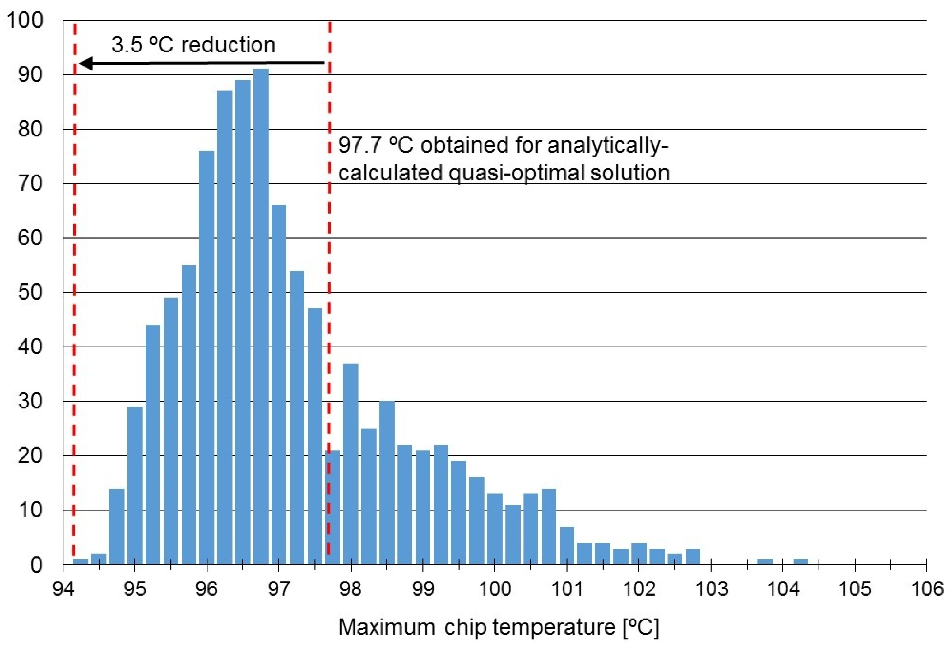
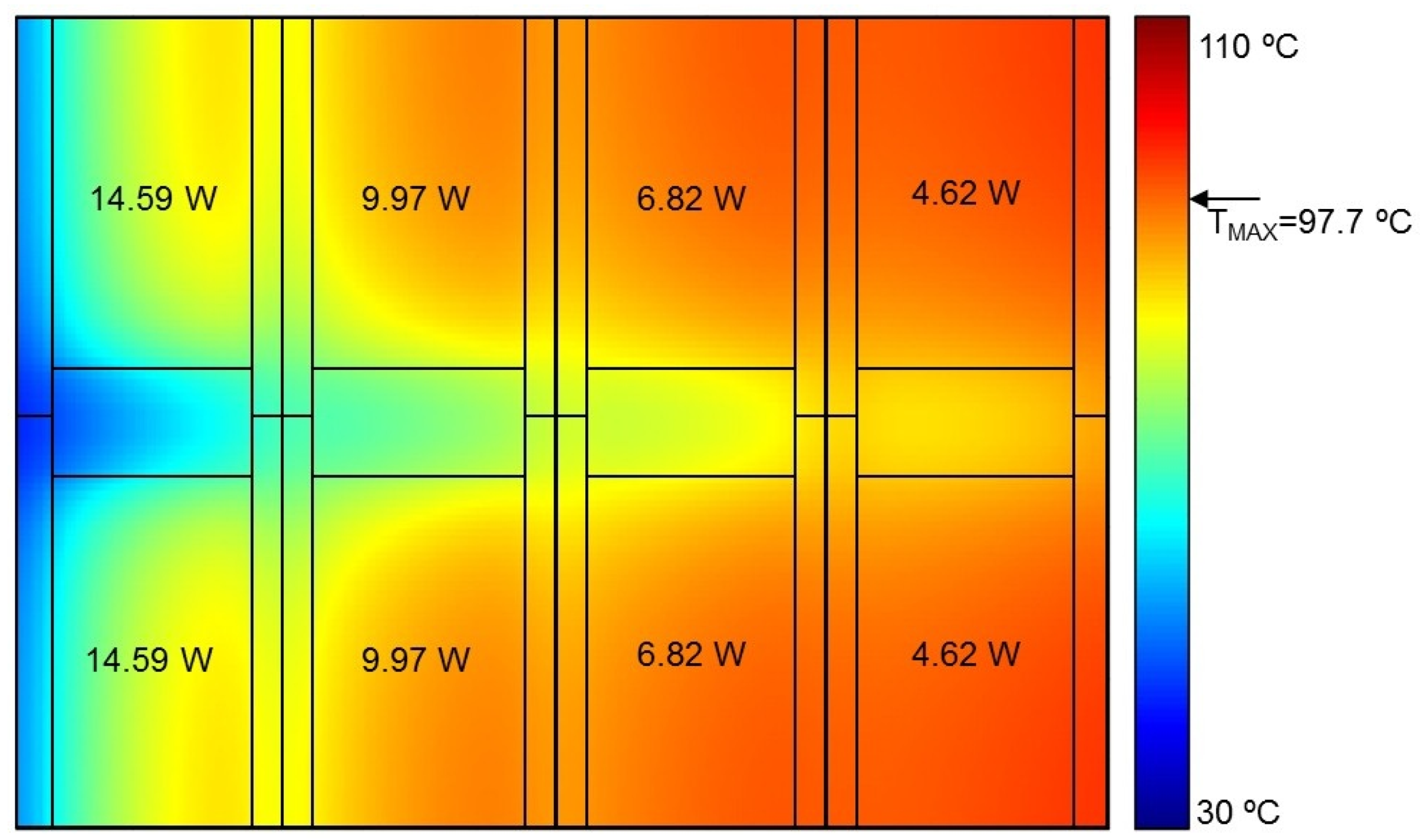
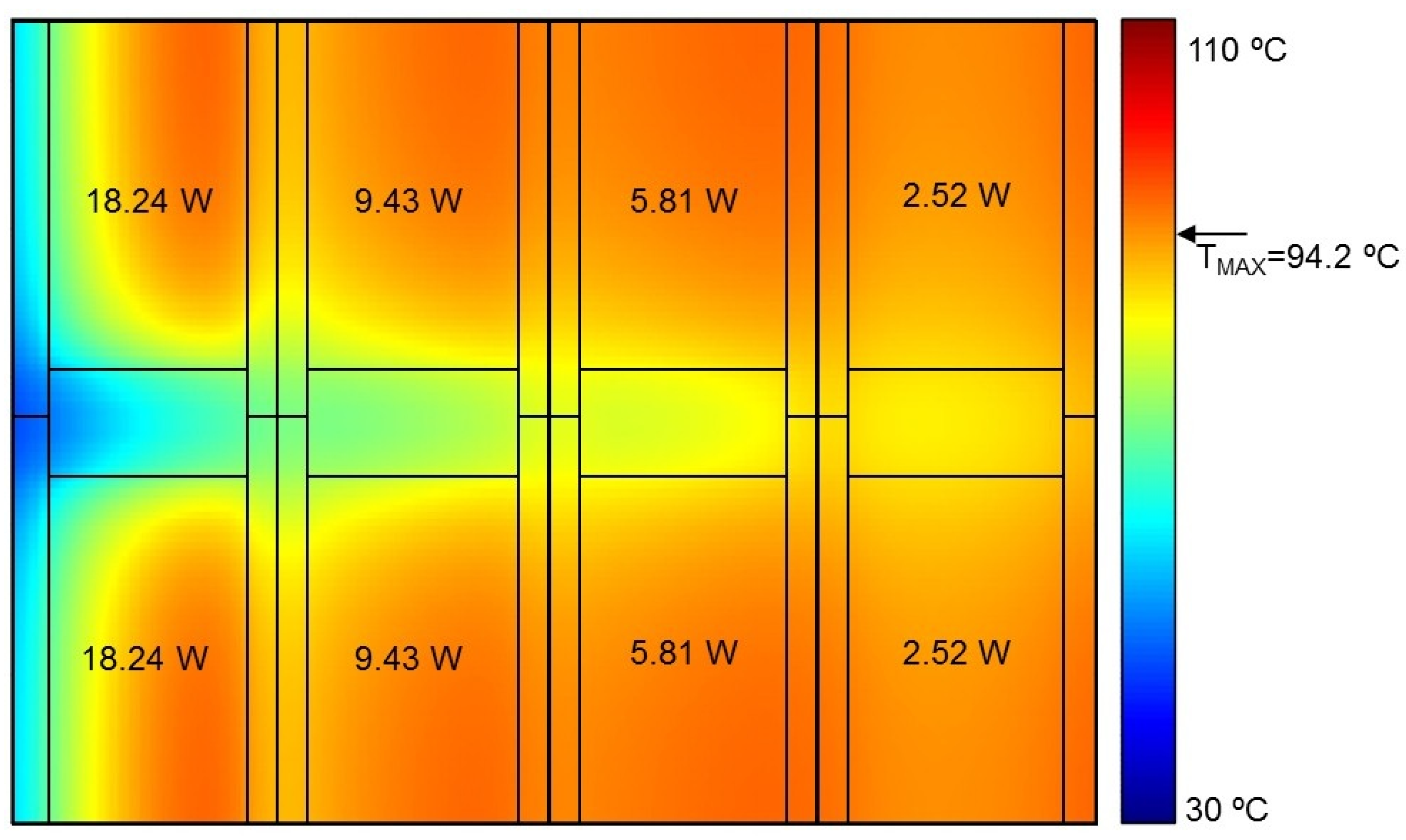
Table 3 shows the power values obtained using the above method for the analyzed 3D processor. However, the formula from (3) was derived for a constant HTC along the channel and does not take into consideration the thermal entry effects (higher HTC near the inlets). It can be safely supposed that the true optimal power distribution will be more uneven, with even more power dissipated in cores near the inlets. Thus, additional simulations were run: taking the previously calculated power distribution as a starting point, the power consumption in cores near the inlets was increased and in cores near the outlets decreased (keeping the total power constant). It was discovered that it was still possible to reduce the peak temperature using this method. Thus, it was proven that the power values calculated analytically are in fact a quasi-optimal solution, and a better solution can be found. Consequently, a Monte Carlo method was employed: 1000 simulations were run, and for each core the power was generated randomly within a certain range around the previously found quasi-optimal values. Again, the total power was kept constant. The simulation results are shown in
Figure 8. The lowest maximum temperature was obtained for the power values shown in
Table 3 (right column). It was 3.5 °C lower that the one obtained for the quasi-optimal solution.
Additionally,
Figure 9,
Figure 10 and
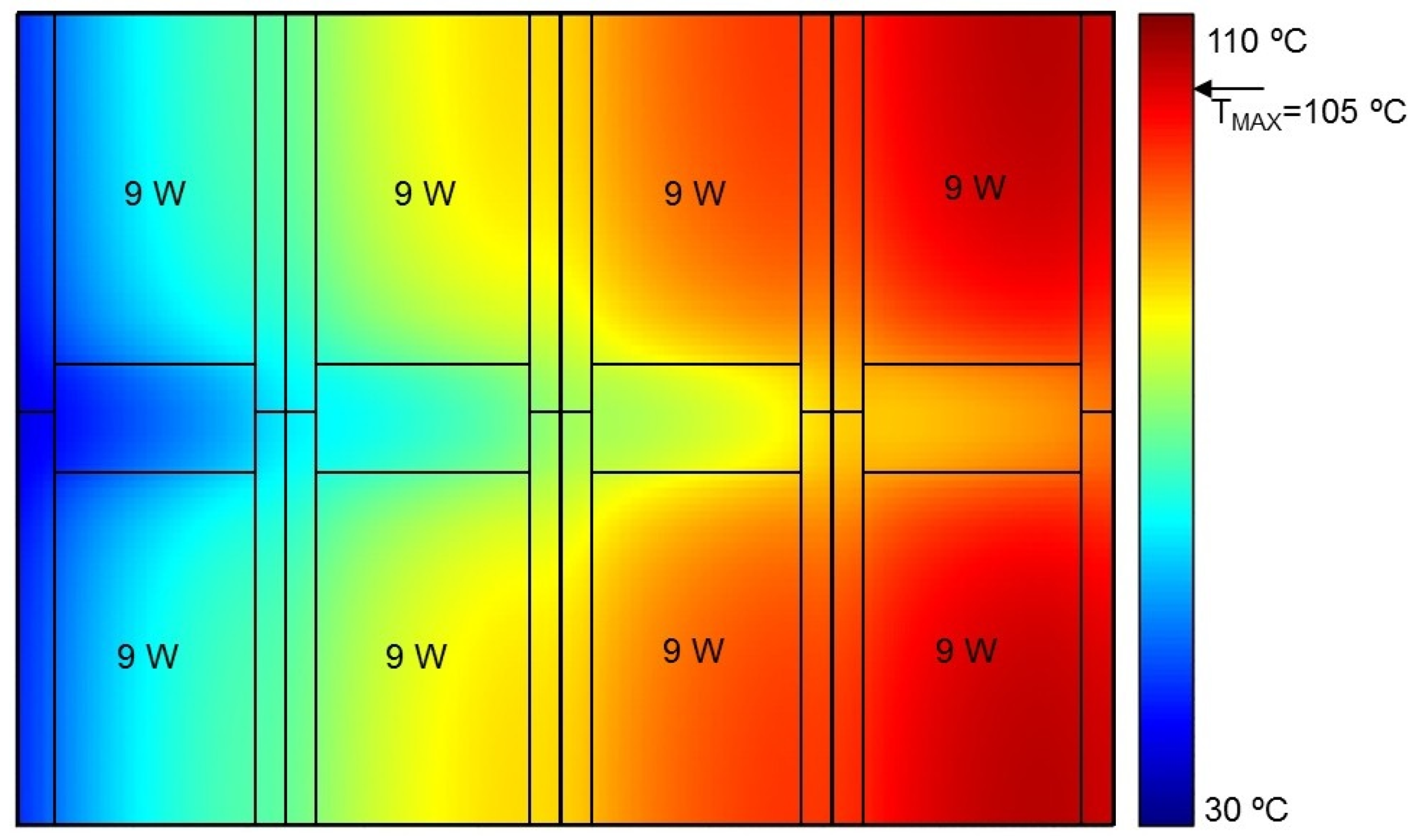
Figure 11 show the temperature maps of the middle chip layer for three cases: one with uniform power distribution in cores; one with quasi-optimal power distribution; and one with optimal power distribution, respectively. The temperature maps were superimposed on the chip floorplan for clarity. By comparing the three figures, it can be clearly seen that the more uniform the temperature distribution in all cores, the lower the maximum temperature in the chip. Therefore, it may be argued that the optimal power dissipation in cores should be such that the peak temperature in each core is the same.
There are three main findings that can be derived from the obtained results. First, although the power profile described by Formula (3) allows a considerable reduction in peak temperature, it cannot be seen as the optimal solution. The true optimal power profile contains quite different power values (compare columns two and three in
Table 3). Therefore, for best results, the thermal entry effects should not be ignored when developing efficient DVFS or task scheduling schemes. Second, the optimal power profile is extremely difficult to calculate analytically. However, it was possible to find the optimal power values by running a large number of simulations. Note that this Monte Carlo approach would not be possible with CFD simulation, because the simulation time would be prohibitively long. This highlights the advantages and demonstrates the usefulness of the proposed compact thermal modelling tool, which allows exploring the design space in a reasonable time. Third, which may be surprising, the optimal power profile is very non-uniform (18.24 W for cores near the inlets and 2.25 W for cores near the outlets). This means that more than seven times more power should be dissipated in “inlet cores” compared to “outlet cores”. Even with very aggressive DVFS, this may not always be possible to achieve. Therefore, for microchannel-cooled processors, the designers should perhaps consider floorplanning schemes which take this effect into consideration, e.g., processing cores should not be put near the outlets, and this outlet area should be reserved for processor units with low power dissipation.
5.3. Power Distribution Correlation Metric
Knowing the optimal power consumption in each core allows introducing a metric which describes how a given power distribution correlates with the optimal one. In other words, every possible power distribution can be quantified in terms of how similar it is to the optimal distribution, which in turn allows choosing the best one, for example when executing thermal-aware task scheduling or calculating the best DVFS settings.
Let
Poi be the optimal power dissipation calculated for core
i and
Pi the actual power consumption in core
i. Let us define
Tmax as the maximum chip temperature. In the first approach, one may think than
Tmax will be strongly correlated with the maximum difference between
Pi and
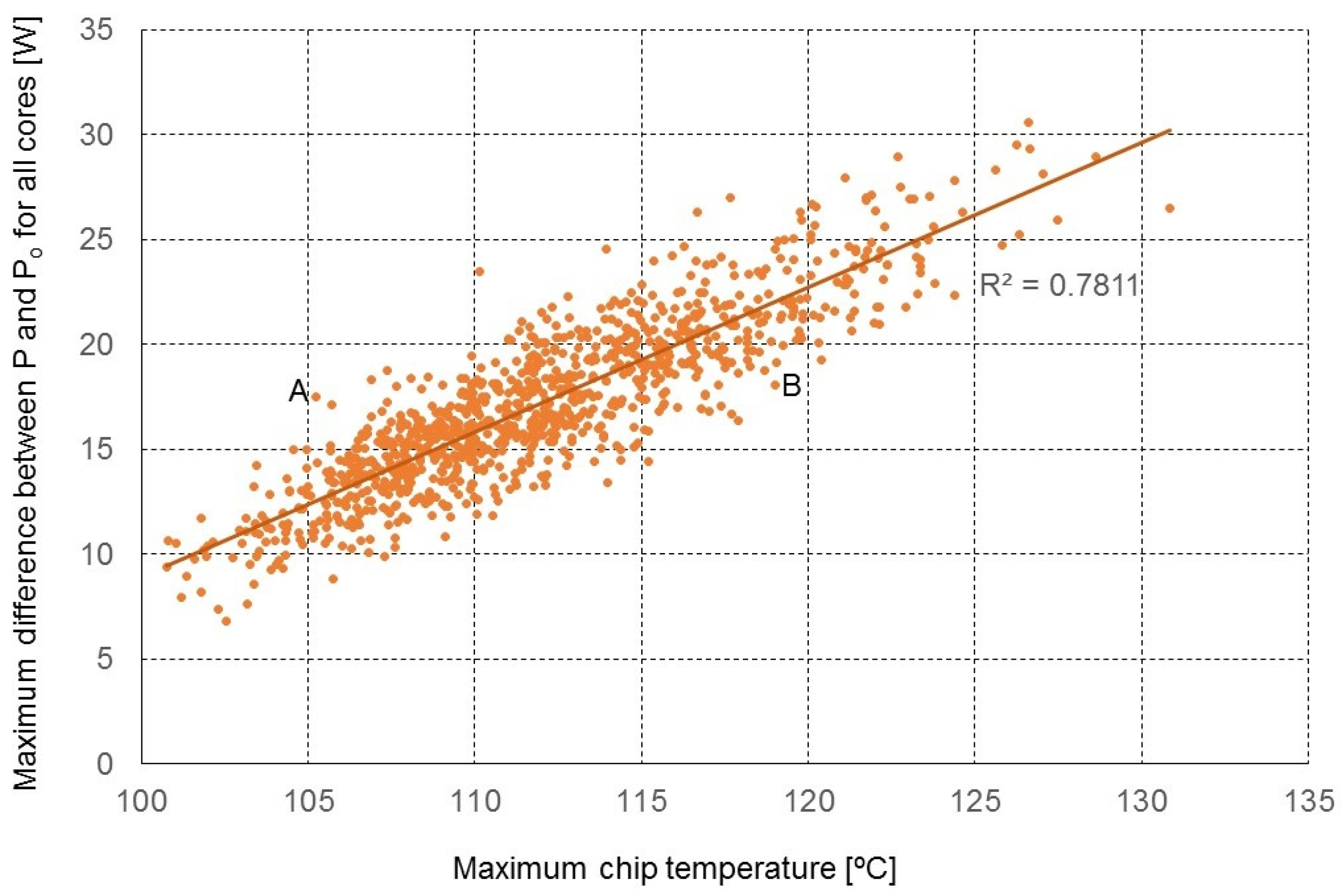
Poi calculated for all cores. To verify this hypothesis, 1000 simulations were run, with random powers generated for all cores while keeping the total power constant.
Figure 12 shows the correlation between such a metric and the maximum chip temperature. We can see that this correlation is certainly visible, but the variance is still quite high. For example, let us look at the points A and B in the figure. For the same value of the metric, the difference in peak temperature is around 14 °C, so this metric would not produce satisfactory results and a more accurate approach is needed. Hence, a simple thermal model is proposed here. Consider a one-channel system and the area located at the distance
x from the inlet. The temperature of the fluid at location
x can be approximated as:
where
Ti is the fluid inlet temperature,
is the mass flow,
cP is the specific heat of the fluid and
QU is the power dissipated upstream from the location
x. The temperature of the solid at point
x can then be calculated as:
where
h is the heat transfer coefficient between the solid and the fluid,
A is the channel area through which the convection occurs, and
Q is the power consumption in the area. Equation (5) can then be reformulated to describe the overhead in peak temperature Δ
T:
where Δ
QU is the overhead power dissipated upstream from location
x and Δ
Q is the overhead power consumption in the area. The overhead power is, of course, calculated as the difference between the actual power and the optimal power. Δ
T is the overhead peak temperature: the difference between the actual peak temperature and the temperature resulting from the optimal power.
Although Equation (6) was derived for a one-channel system, it can be applied to estimate Δ
T for each core in the chip and then to calculate the maximum of these values Δ
Tmax. Note that, in this case, Δ
Tmax does not give any information about the absolute value of the maximum temperature in the chip; it is simply a relative metric which can be used to compare power distributions. For example, a power distribution with a higher value of this metric will always produce higher maximum temperature and vice versa. Achieving the linearity of the metric is also important. To make this metric dimensionless, it was further divided by inlet temperature
Ti. Again, 1000 random-power simulations were run to test the correlation of the metric with the chip peak temperature.
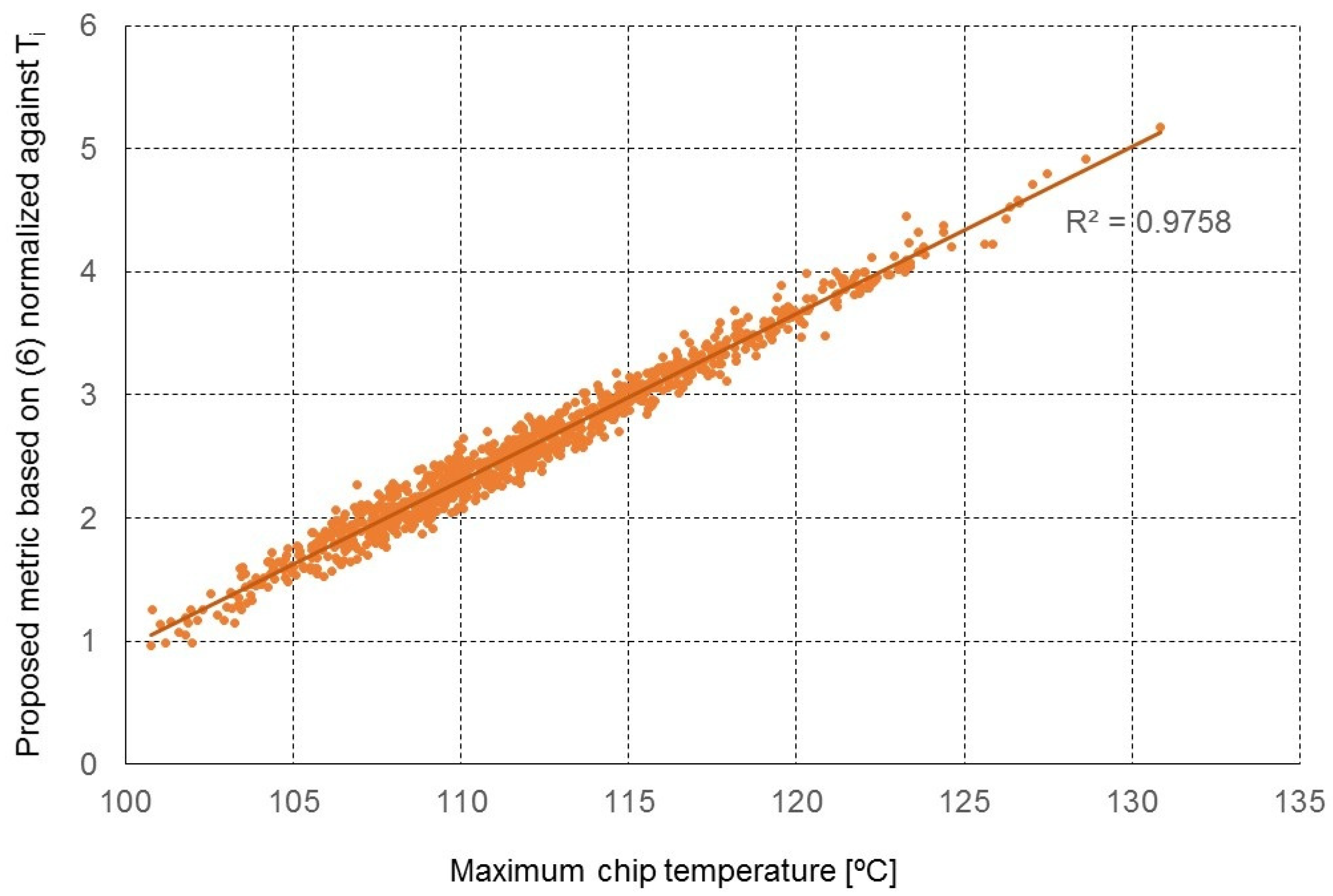
Figure 13 shows the obtained results: despite the fact that the used model is relatively simple, we can see that the linearity of the model is surprisingly good and that this metric can be effectively used to predict which power distribution is better, i.e., which power distribution results in lower maximum chip temperature.
In what follows, the utility of the proposed metric will be discussed. The main advantage is that it is very simple: the optimal power distribution has to be found only once for a given chip. Then, the metric can be easily calculated analytically, so the cost (for example in terms of time or energy) of calculating this metric is negligible. Therefore, it can be used not only in static, but also in dynamic task scheduling algorithms. Such an algorithm could use, for example, the cooling performance coefficient CPC for each processor core, calculated as the inverse of the proposed metric. Then, assuming that a set of tasks is to be scheduled on cores, the algorithm can utilize the calculated CPC values to find the optimal mapping, thus guaranteeing the lowest possible peak temperature in the chip during task execution. It can be also used to for efficient task swapping: if new tasks appear, a new optimal mapping can be found on the fly, and all tasks (including those already being executed) can be rescheduled to different cores. Similarly, researchers who develop DVFS algorithms can make use of the proposed metric to dynamically adapt the voltage and the frequency of each core. For example, taking as input the estimated power of tasks to be executed, the dependencies between them and their potential deadlines, the algorithm can find the optimal frequencies and voltages for the cores which result in the minimization of the peak temperature during task execution.


