Article

Bifacial p-Type PERC Solar Cell with Efficiency over 22% Using Laser Doped Selective Emitter

1
College of Materials Science and Technology, Jiangsu Key Laboratory of Materials and Technology for Energy Conversion, Nanjing University of Aeronautics and Astronautics, Nanjing 210016, China
2
Jiangsu Sunport Power Corp., Ltd., Wuxi 214028, China
3
Jiangsu Collaborative Innovation Center of Photovoltaic Science and Engineering, Changzhou University, Changzhou 213164, China
*
Author to whom correspondence should be addressed.
Energies 2020, 13(6), 1388; https://doi.org/10.3390/en13061388
Submission received: 31 January 2020 / Revised: 25 February 2020 / Accepted: 12 March 2020 / Published: 16 March 2020
(This article belongs to the Section A: Sustainable Energy)

Abstract

:
In this paper, we report one bifacial p-type PERC solar cell with efficiency over 22% using laser doped selective emitter produced in larger-scale commercial line on 6-inch mono-crystalline wafer. On front side of the solar cell, square resistance of p-n junction was found to be closely related with laser power at certain laser scan speed and frequency. On the other side, the rear fingers with different ratios of height and width and rear silicon nitride (SiNx) layer with different thickness were optimized, and a highest rear efficiency of the bifacial solar cell was obtained. Finally, bifacial silicon solar cells with the front and rear efficiencies exceeding 22% and 15% (AM1.5, 1000 W/m2, 25 °C) were successfully achieved, respectively.

1. Introduction

In recent years, more photovoltaic companies and researchers [1,2] began research and production of silicon bifacial solar cells and passivated emitter and rear cells (PERC) based on p-type crystalline Si wafers are mainstream high-efficiency cell technology although most of the advanced cell technology has their own dual-generation properties. The performance of industrial-type screen-printed 6-inch PERC solar cells has been significantly increased over the past few years. PERC solar cell efficiencies surpassing 22% have been reported [3]. Normally, mainstream p-type PERC cell efficiency is about over 21% [4]. Therefore, p-type bifacial PERC cell is predicted to be the cell technology with the largest gain in market share in the next few years.
The efficiency of the c-Si (crystalline silicon) solar cells with traditional homogeneous emitter fabricated in the screen-printed metallization process is limited by inherent limitations [5,6]. Forming a selective emitter is an effective solution to overcome these limitations and increase the cell efficiency [7,8,9,10,11]. However, selective emitters have not yet been commercialized in practical manufacturing in the last ten years, mainly because creating a selective emitter is very complex, and the cost of cells is quite high [12,13,14]. The main methods of forming selective emitters include oxide masking, screen printing silicon ink, ion implantation and laser doping. In order to lower the thermal budget and make the process more compatible with the existing standardized production line, laser-doping (LD) was proposed as an alternative way to form the selective emitter [15,16,17,18,19,20]. For PERC cell production line, selective emitter (SE) based on PERC cell has more advantages than that based on regular p-type cells.
Bifacial silicon solar cell is a special kind of crystal silicon solar cell structure, which can receive sunlight and produce electricity power from both front and back sides. These cells are designed with special structure and finger contact, so they can absorb more sunlight and produce much power from both sides. The efficiency gains of bifacial solar cells relative to single-sided solar cells are difficult to measure by single cell. Therefore, in most cases they need to be made into modules. Bifacial modules can be installed flexibly in wide range of applications. The form of conventional single-sided cell module installation application, such as ground photovoltaic power station and roof photovoltaic system, is equally suitable for bifacial modules. The bifacial modules are especially good for ground installation because they take advantage of the ground’s reflected light, generate more electricity under the same conditions, and are also suitable for installation on the roof. Ground and roof mounted bifacial modules should be mounted tilted on the scene. The bifacial cell and module can also be free from the direction of installation. The back is as beautiful as the front, especially suitable for the vertical installation of the scene, such as vertical installation as a fence, soundproof wall, highway guardrail, etc. Therefore, the bifacial modules are suitable for installation in various scenarios, such as ground power station, uniaxial tracking system, water surface power station, sunshine room, photovoltaic shed, highway soundproof wall, curtain wall, car shed, building integrated PV, and so on. Meanwhile in some ground power plant or rooftop power plant, bifacial cells and modules also were installed and have been run steadily for several years [21].
The main advantage of using bifacial solar modules to build photovoltaic power plants is high power generation. Generally, the bifacial cells are made into bifacial modules. When the orientation, inclination and height of the bifacial modules are fixed, the power generation gain of the bifacial modules mainly comes from the back side, which improves the current and maximum output power of the assembly by receiving the atmospheric scattered light and the reflected light of the ground. In addition, the power generation gain of the back can be improved by raising the height of the component and increasing the inclination angle of the component. Such matching tracking bracket can highlight more the stacking advantage of 1 + 1 > 2, which is expected to achieve 20% to 30% of the power generation gain. The power generation gain of the bifacial module is closely related to the practical application scene. Combined with different double-sided illumination conditions, 10% to 30% power generation gain can be realized [22,23].
All the time, n-type bifacial cells were paid close attention to by many PV researchers all the time [24,25,26], and a higher efficiency of solar cell was obtained [27,28]. Currently n-type wafer is much more expensive than p-type wafer and n-type PERC cell process is very complex. The equipment upgrade into n-type PERC cell process line from the p-type cell process line is almost impossible. At the same time, many investors consider that the cost of n-type bifacial solar cells is too high to realize the commercialization of n-type PERC cell process. Therefore, it will be of far-reaching significance to study the p-type bifacial cell and improve the efficiency of the cell to maximize the power generation benefits of the solar system.
In this work, we investigated fabrication of p-type bifacial silicon solar cells, and bifacial silicon solar cells with realizable structure for high efficiency were introduced. The proper technical path was used to fabricate these bifacial solar cells, and p-type silicon wafer was used. The selective emitter in the PERC structure was illustrated in Figure 1. The anti-reflection coating and finger contact were fabricated on both surfaces of the solar cells. The rear fingers with different ratios of height and width and rear SiNx with different thickness were adopted for high rear efficiency, and bifacial silicon solar cells with the front and rear efficiencies exceeding 22% and 15%, respectively, were successfully produced in solar cell production line.

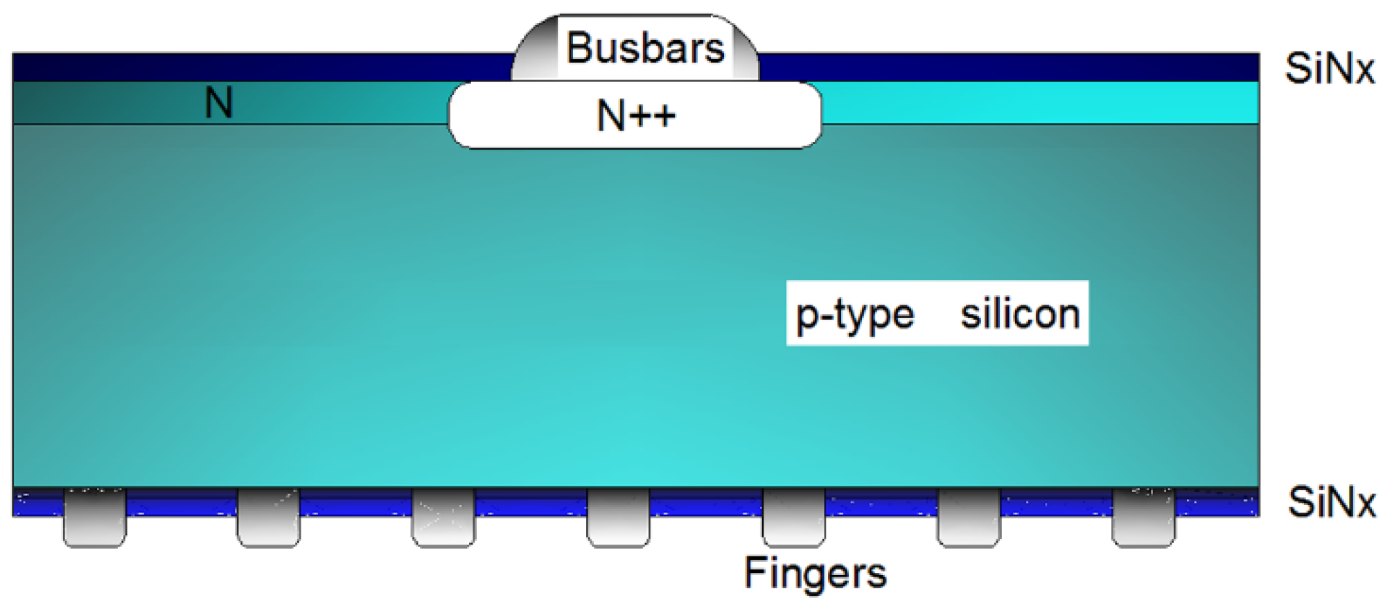
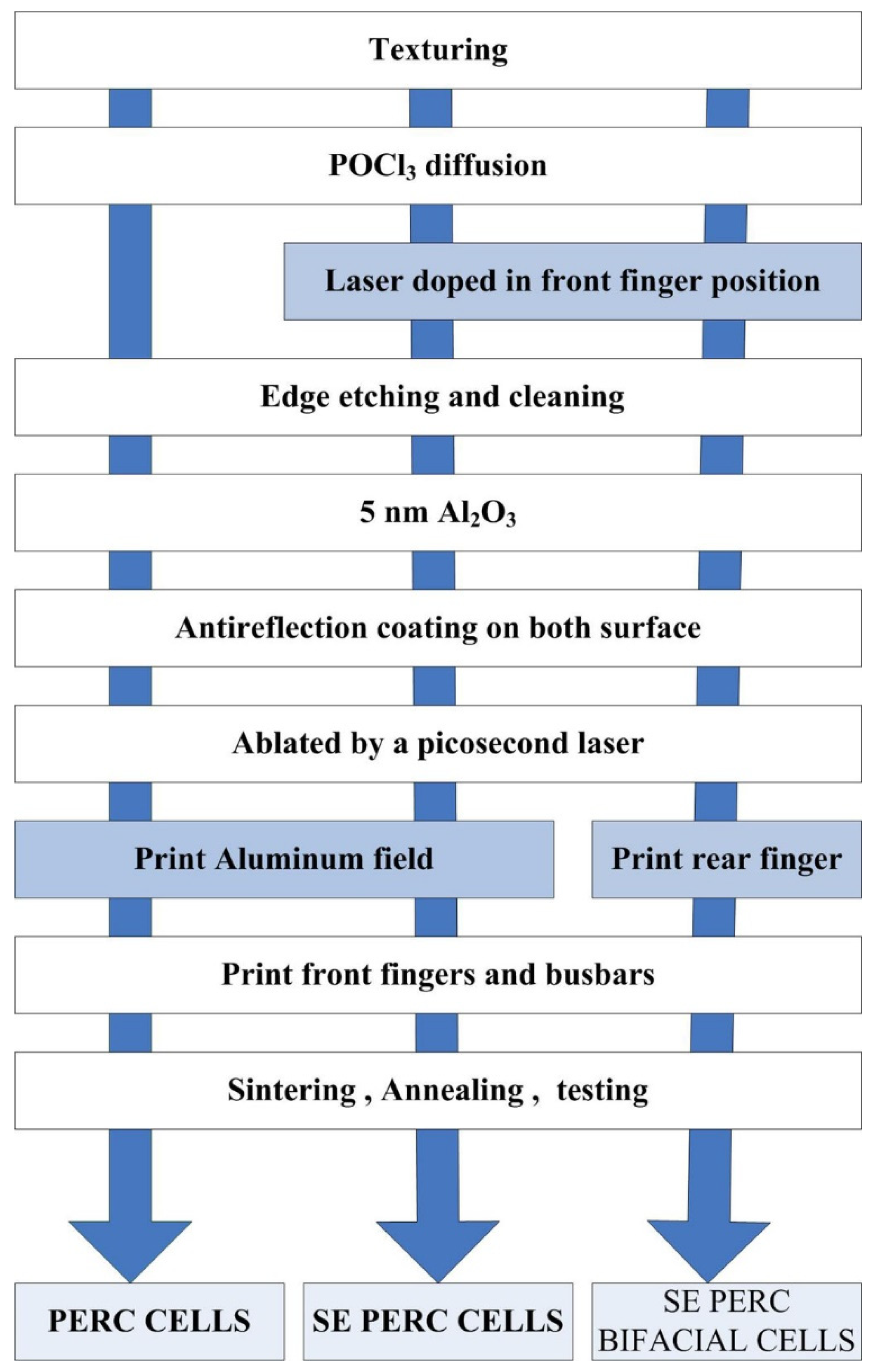
2. Bifacial Solar Cell Fabrication Process

2.1. Cell Fabrication

PERC solar cells were produced in our research and development experimental production line. 1.6-Ω·cm boron-doped Czochralski (Cz)-grown wafers (242.21 cm2) with an initial thickness of 180 μm were used in our experiment. After texturization in front-side (KOH + additives, time 10–15 min, temperature 80–83 °C), the wafers underwent a phosphorous-doped emitter, then laser doping under the busbars and fingers region with phosphorosilicate glass. Diffusion square resistances in lightly doped region and in heavily doped region were 130 and 85 Ω/□, respectively, according to measurement results by 4-point probe. On the front side, 80 nm SiNx (n = 2.10 at 632 nm, NH3: 7000 sccm, SiH4: 730 sccm, Time: 850 s, temperature: 15 min, power: 6800 w, pressure: 1500 mTorr) was deposited by plasma-enhanced chemical vapor deposition (PECVD). On the rear side, we deposited a stack of 5-nm-thick Al2O3 (time 150 s, temperature 300 ± 30, pressure 6 ± 2 mba, PM H2O push 30 ± 20 slm) and 70~110 nm-thick SiNx (parameters range (NH3: 7000 sccm, SiH4: 730 sccm, Time: 400–850 s, temperature: 15 min, power: 4000–6800 W, pressure: 1400–1800 mTorr)). The Al2O3 layer was deposited by atomic layer deposition and the SiNx layer by PECVD. The dielectric layers were ablated by a picoseconds laser for line contact formation. The front side metallization was realized with regular screen-printing technology.
In order to realize the structure of bifacial solar cells with a simple technical flow, we redesigned the fabrication flow and compared the regular PERC and SE PERC cell technical flow, which was shown in Figure 2. The different technique between regular PERC and SE PERC was laser doping. However, the difference between bifacial PERC solar cell and one-sided PERC cell was printing rear finger. One-sided solar cell needed printing aluminum field without busbars and fingers for the rear side of cells. Certainly, back polishing in tech and cleaning process was also necessary but it was not within discussion in the present work.

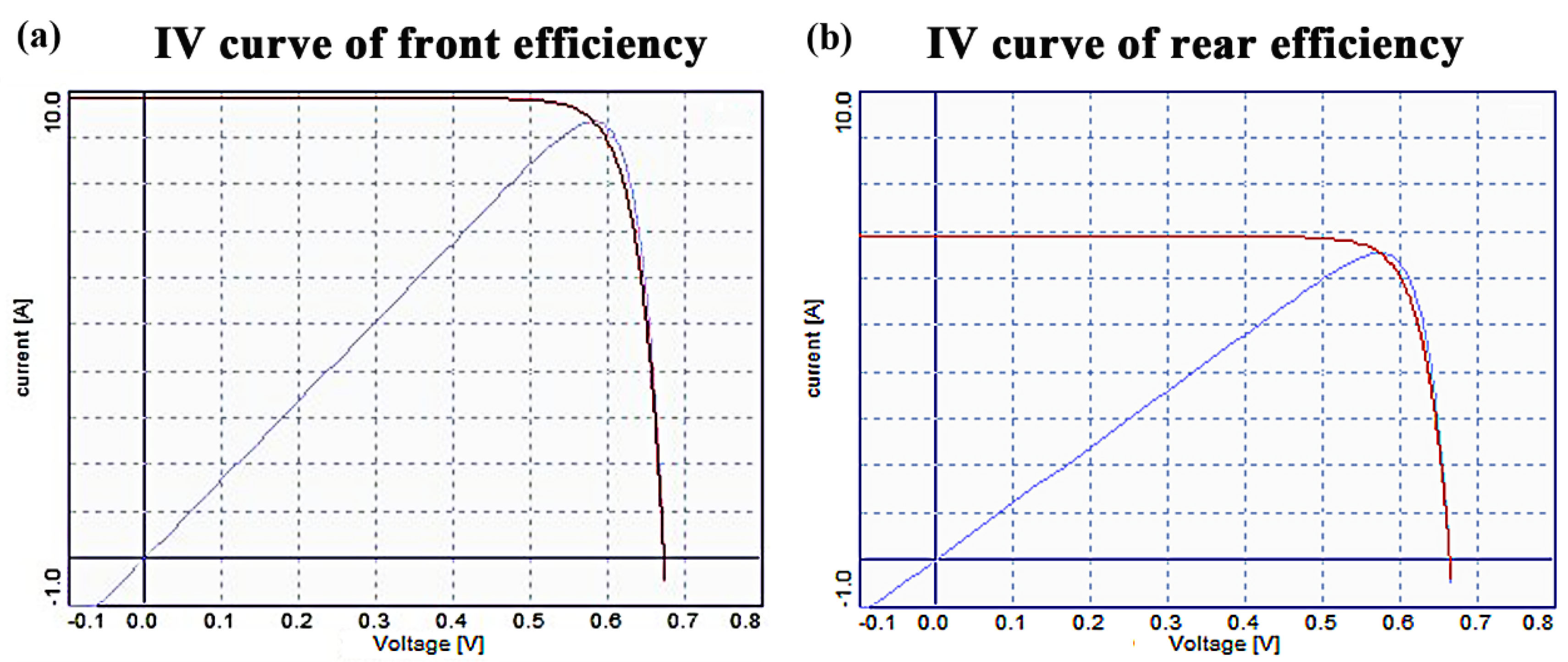
2.2. Characterization

Square resistance was measured by four-point probe method, and five points were tested in each wafer. Laser doped position and screen print line width was observed by microscope (KEYENCE VN-2500R). A picture of height and width of rear fingers was taken by three-dimensional microscope (ZETA-20). Thickness of SiNx layer was measured by laser ellipsometer (EMPro-PV). Front and rear I-V curves and detailed electric data were measured under the simulated AM1.5 (air mass 1.5) sunlight at 1000 W/m2 irradiance, generated by a light source of AAA simulator on the h.a.l.m. system.

3. Results Discussion and Analysis

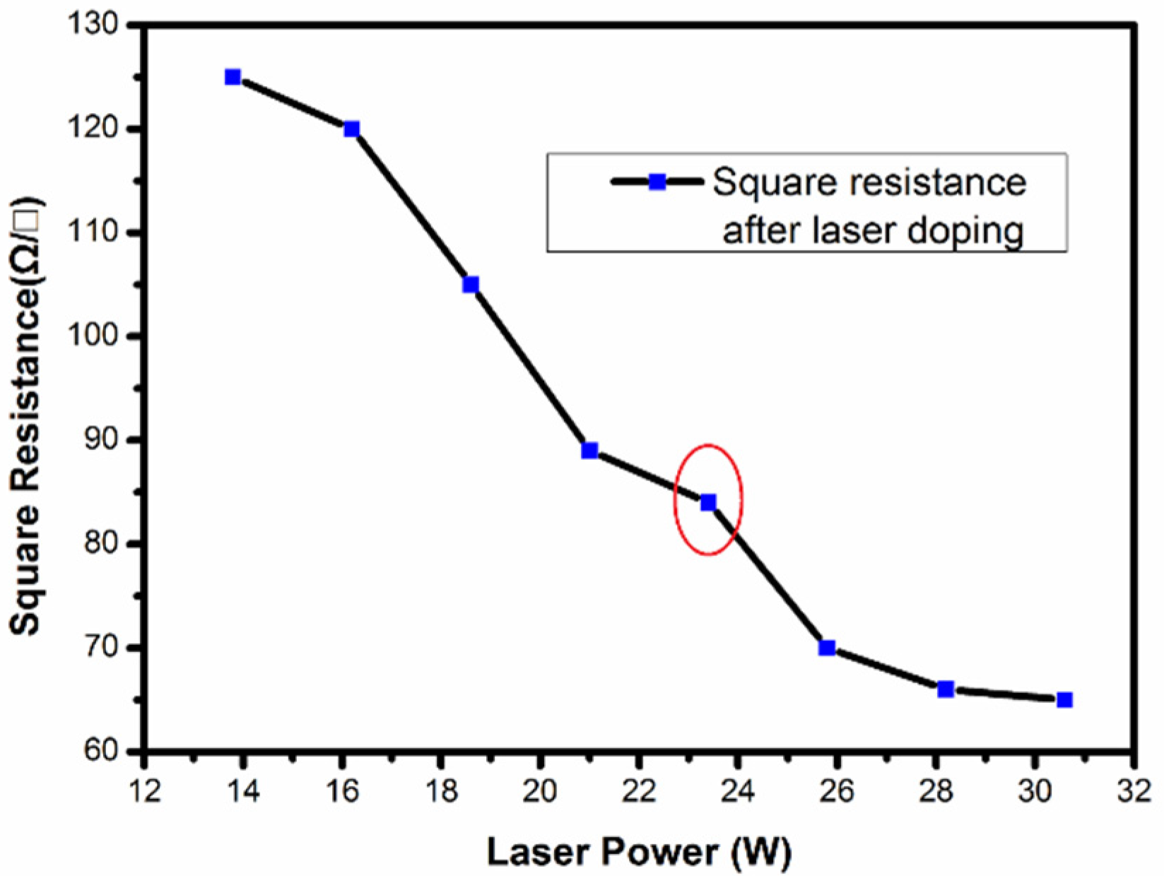
3.1. Laser Doping and Resulting Square Resistance

For emitter of solar cell, lower square resistance will reduce contact resistance and series resistance, but in this case, carrier recombination would increase, and the lifetime of minority carriers would correspondingly decrease to reduce Open-Circuit Voltage (Voc) and Short-Circuit Current (Isc) of the solar cell. On the other hand, higher square resistance would decrease carrier recombination and raise the lifetime of minority carriers, but it also would increase the contact resistance, leading to a higher series resistance. Selective emitter can combine the higher square resistance and the lower square resistance on the different region to create lower carrier recombination on higher square resistance region and lower contact resistance on lower square resistance region then to get a higher efficiency. In our work, different square resistance was designed via laser doping in the emitter region. Source of laser doping is phosphorosilicate glass (PSG) that is a byproduct of POCL3 diffusion in step 2 in Figure 2.
After POCL3 diffusion,130 Ω/□ square resistance was realized (step1: temperature 790 °C, deposition 15 min, N2/O2 = 1:1; step2: temperature 845 °C, drive in 13 min) and n+ layer of p-n junction was doped into n++ layer by laser with high power, using short wave laser equipment on the corresponding region of the front electrode and finger.
Normally laser spot distance is controlled by changing scan speed. Spot distance responses scan speed/frequency. The lower scan speed, the higher the degree of overlap is, which will reduce square resistance. High square resistance will induce lower surface concentration and higher contact resistance. Certainly, laser spot distance also was controlled by changing frequency. In our experiment, firstly the laser debugging interface was opened after equipment was powered on. Then the laser power of about 10 W was set. Before laser device was turned on, the laser light source should be preheated for 5–10 minutes to reach a stable operation temperature of about 150 °C. The button “Open Carving Graphic” in the operation software was clicked to select the laser carving graphic, which corresponded to the front electrode and finger region, and square spot size of 120um was set. Some parameters such as 515 nm laser wavelength, 100 KHz frequency, and 18 m/s maximum speed were fixed in our experiment. One batch of wafers with the same light diffusion of 130 Ω/□ and the same thickness PSG after diffusion was prepared, and then, the different laser power was adjusted, and doping was carried out. After doping different piece of wafers with the same light square resistance by each fixed laser power, different groups of wafers with different square resistance on heavy diffusion region were obtained. After testing square resistance of every group of wafers (four-point probe method, five points tested in each wafer), relationship between laser power and square resistance after laser doping was found as shown in the following Figure 3.
A compatible square resistance was found in 23.4 W as shown red circle in Figure 3. At the same time, it could be seen from Figure 3 that square resistance in heavy diffusion region after laser doping became more lower when the larger laser power doping was carried out on the same wafers with lightly diffused 130 Ω/□ and the same thickness PSG.
Average square resistance of 85 Ω/□ was obtained by laser doping with a reasonable power of 23.4 W on 50 nm thickness phosphorosilicate glass (PSG). Then, 85 Ω/□ and 130 Ω/□ average square resistances corresponding to heavy diffusion and light diffusion were found to be a best combination. For the experiment process, local square resistance with 85 Ω/□ ± 5 and 130 Ω/□ ± 5 should be well balanced. Uniformity of square resistance in each wafer should be lower than 12%, and uniformity of square resistance between two wafers should be lower than 8%, which was equal to (max–min)/2 * average of square resistance. Then the residual PSG on the laser-irradiated surface was removed by HF dipping after laser doping.

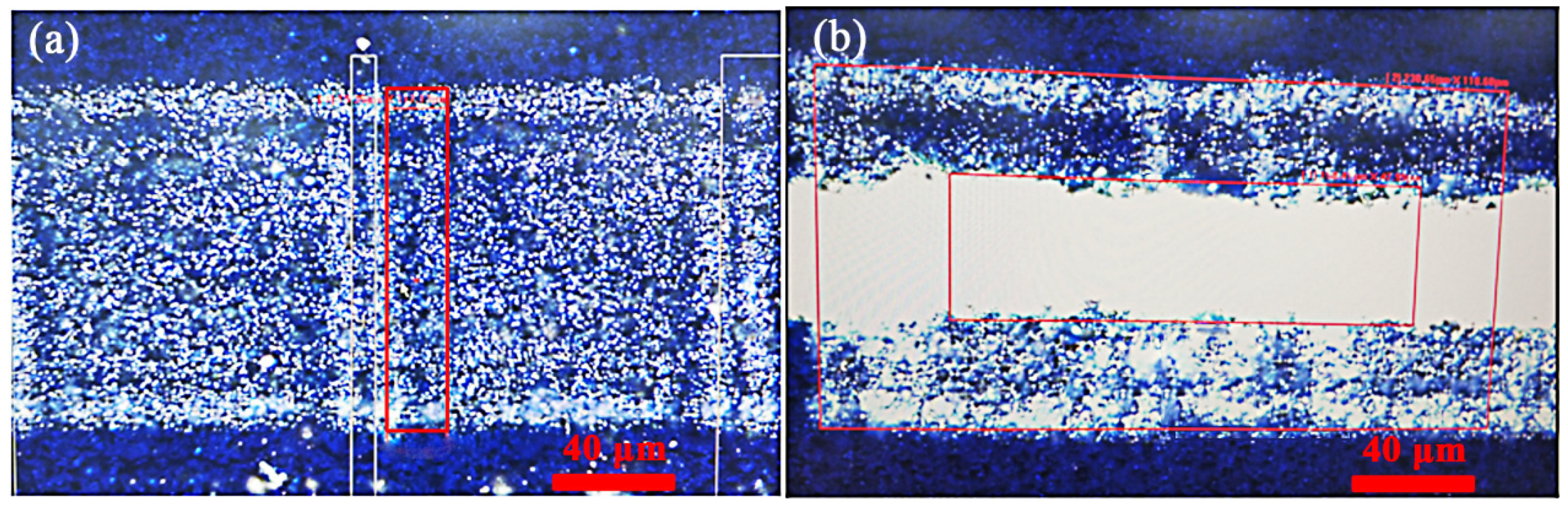
3.2. Laser Doping Region and Overprint Effect in front Finger

Instead of the typical four busbars, the cells featured five 0.7-mm-wide busbars on the front side in order to reduce the series resistance by the metal fingers. For collecting the more photon-generated carriers and getting higher conversion efficiency, more fingers were used than those used in regular cells and the quantity of fingers is 110 in the front side of solar cells. In our design, every printed finger should be overlapped with laser doped position as shown Figure 4b. Laser doping line width is 118 μm as shown Figure 4a and screen print of Ag finger with 40 μm should be overprinted within laser doping line so that maximum of allowable screen-printing deviation of 39 μm as shown in Figure 4b could be realized.
As shown in Table 1, an efficiency enhancement of 0.35% of SE PERC solar cell was realized than that of regular PERC cells resulting mainly from higher Isc and Voc values. Isc value was raised from 9.93 A to 10.03 A, with 0.1A gain, and Voc value was improved from 0.657 V to 0.673 V. In our experiment, the square resistance of regular PERC cells by POCL3 diffusion was 95 Ω/□ (step1: temperature 790 °C, deposition 15min, N2/O2 = 1:1; step2: 865 °C, drive in 13 min).
But if overprint in laser doping region was improper, the efficiency of the solar cell would be greatly reduced, even lower than that of regular PERC solar cell. As can be seen from Table 1, the efficiency (Eff in Table 1) of improperly printed SE PERC cell was 21.47% while the efficiency of regular PERC cell was 21.88%. The about 0.4% reduction was mainly due to the drop of fill factor (FF in Table 1) value. The larger series resistance (Rs in Table 1) value, with a difference of 0.001 Ω compared with that of the best SE PERC group, illustrated that there was an unfriendly contact between finger or busbars and emitter.

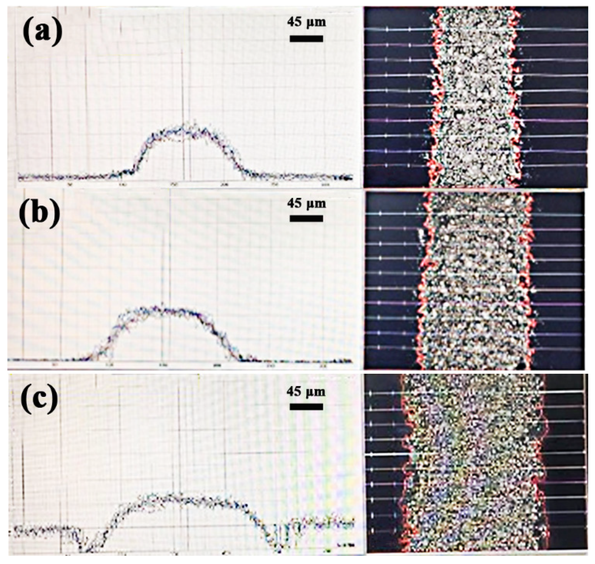
3.3. The Influence of Ratio of Height and Width in Rear Finger

On the rear side, five busbars in parallel lines matching with the front busbars position were also applied, but the quantity of fingers (150) was more than those on front side. As we all know, narrow metal front side coverage will result in a decrease of shadowing and surface recombination but an increase of resistive losses [29]. The second printing with narrow fine fingers would compensate the losses by large resistance and lead to the excellent Voc, Isc, FF, and Eff [30].
In the present work, standard single-printed Al metallization design was used rather than second-print metallization design in the rear side. Three different printing screen line widths (80 μm, 100 μm, 150 μm) were used in our experiment. One batch of wafers was divided into three groups in screen printing process (previous procedures such as diffusion were the same) and printed with three different sets of screens followed by firing process and solar cells were produced. Total cell numbers for the three groups are 1210 pieces in 80 μm group, 2440 pieces in 100 μm group and 294 pieces in 150 μm group. In addition, special aluminum paste 8401A from Rutech, a professional paste company, for PERC bifacial cell in rear side was used.
At the same time, one piece of cell from every group was selected to measure the height and width of rear fingers. A picture was taken to represent each group of fingers in Figure 5. In Figure 5, height and width of the waveform in picture (a) show the height and width of the 80 um group finger. Values of height and width in picture (a) are shown as column 2 and 3 (height 19.28 μm and width 113.49 μm) in Table 2. The right to picture (a) is its two-dimensional photo for 80 μm finger. Height and width of the waveform in picture (b) show the height and width of the 100 um group finger. Values of finger’s height and width are shown as columns 2 and 3 (height 21.34 μm and width 143.01 μm) in Table 2. The right to picture (b) is its two-dimensional photo for 100 μm finger. Height and width of the waveform in picture (c) show the height and width of the 100-um group finger. Values of the height and width are shown as column 2 and 3 (height 11.08 μm and width 203.87 μm) in Table 2. The right to picture (c) is its two-dimensional photo for 150 μm finger. Ratio of height and width (column 4 in Table 2) is calculated according to following formula.
Ratio of height and width = (height (μm)/width (μm)) × 100
* Ratio of height and width is the factor evaluating size of finger. Height and width were taken by three-dimensional microscope.
In Table 2, 100 μm width of screen group in three groups showed a best electronic performance and the best average FF was 80.41%, corresponding to 14.92% ratio of height and width for rear fingers. Normally a high ratio of finger height and width was desirable for high efficiency solar cell. The narrower finger, the less finger shade area was, which could make more light into p-n junction. However, in practical use, due to the limitation of technical level, the contact interface between aluminum and Si materials would possibly form hollow, which increases the local contact resistance of aluminum and silicon. Certainly, the laser contact openings could be increased, but too deep and wide laser openings would lead to wafers damage which would affect the mechanical character of cells. At the same time, if the finger is too narrow, difficulty of screen printing and the probability of broken finger line would be increased. Therefore, in our work, the efficiency in 80 μm finger group was shallower than that in 100 μm group, resulting from lower FF value.

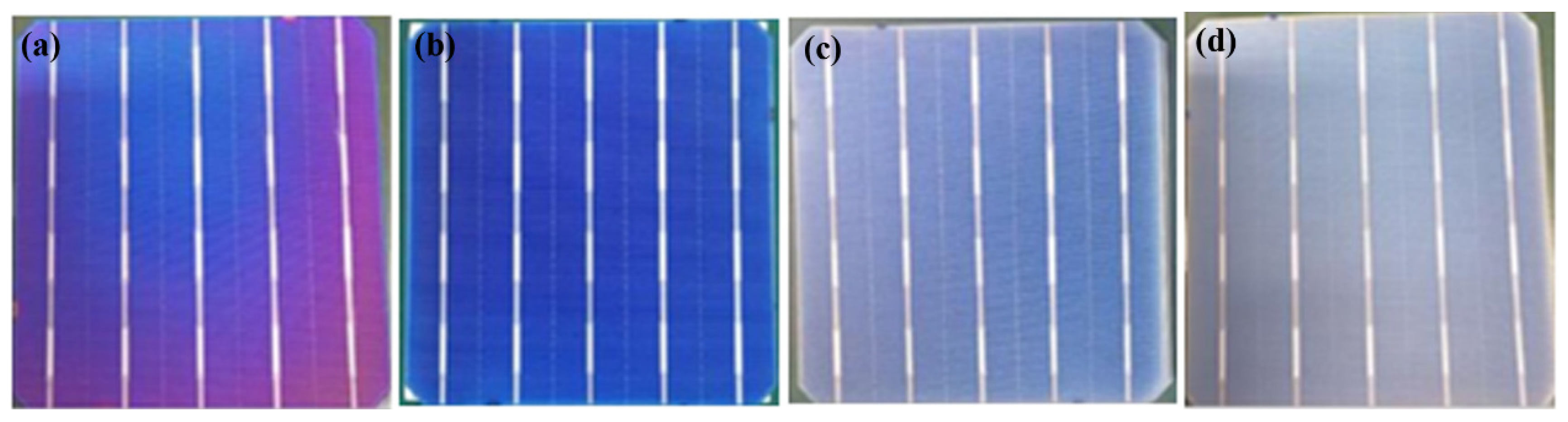
3.4. Dependence of SiNx Layer Thickness in Rear Side

Four different thickness SiNx thin films were fabricated to optimize rear efficiency. Thickness of SiNx film was adjusted from 70 nm to 110 nm. Total cell numbers for the four groups are 46 pieces in 75 nm group, 72 pieces in 80.4 nm group, 84 pieces in 95 nm group, 45 pieces in 104.3 nm group and additional 50 pieces single-side cells group as baseline. Then four kinds of cells with different rear SiNx thickness were produced as shown in the following Figure 6 and detailed electric data of bifacial cell with different thickness SiNx.film were shown in following Table 3. Parameter range (NH3: 7000sccm, SiH4: 730 sccm, Time: 400–850 s, temperure: 15 min, power: 4000–6800 w, pressure: 1400–1800 mTorr) was adjusted for each group.
Bifaciality of bifacial cell in Table 3 is calculated according to following formula.
Bifaciality of bifacial solar cell = (Rear efficiency/Front efficiency) × 100
Bifaciality is bifacial factor evaluating the power generation capacity of the back relative to the front of the cell, usually expressed as a percentage. Front efficiency is the front efficiency of the cell measured when there is non-irradiated on the cell backside under standard test condition (STC: AM1.5 atmosphere profile, 1000 W/m2 illumination, 25 °C). Rear efficiency rear is the rear efficiency measured when there is non-irradiated on the front of the cell under standard test condition (STC: AM1.5 atmosphere profile, 1000 W/m2 illumination, 25 °C). The above calculations should be calibrated according to IEC 60904-7.
According to experiment results in Table 3, efficiency and VOC of solar cell increased with rear SiNx thickness. 104.3-nm-thick SiNx had a best front efficiency but the rear efficiency was lower than that of group (c). Normally the thicker the thickness of rear SiNx was, to a certain extent, the passivation ability of bifacial solar cell could be more improved. At the same time, more photons will be reflected back to p-n junction when the photons in the long wave band reached the rear side of the p-n junction, so that more photon-generated carrier would be produced, thus improving the front conversion efficiency of solar cell. However, if the rear SiNx was too thick, then the photons from the back side needed to pass through the thicker passivating layer in order to reach the p-n junction. The light into the p-n junction would become less and the current would become low, which could affect the rear efficiency. On the other side, if the SiNx layer is too thin, the Al paste is locally firing through the SiNx layer thereby forming additional parasitic Al contacts which increase contact recombination, so as to affect the cell efficiency.
Advantage of bifacial cell mainly depended on two side electricity power output so it was advisable that front efficiency of bifacial cell kept the similar or same level with regular single-side PERC cell and the rear efficiency was maintained at a high level in order to maximize the benefits in practical applications. 95nm-thickness SiNx was perfect to get a highest bifaciality (69.11%) and front efficiency (Voc~0.676V, Isc~9.96A, FF~80.13% and Eff~22.27%), close to regular PERC cell.
The highest front and rear I-V curves were shown in the following Figure 7.
From all of the above data, a highest front cell efficiency of 22.27% (Voc~0.676 V, Isc~9.96 A, FF~80.13%) and a highest rear cell efficiency of 15.39% (Voc~0.663 V, Isc~6.98 A, FF~80.53%) were achieved in this work. In the same time, a trend was found that the small increase of Voc value would affect the cell efficiency greatly. In the actual power plant operation, Isc value would be affected by the actual sunshine light intensity, which fluctuates greatly, but the Voc value fluctuates little. The double-sided cell was mainly affected by the increase of light intensity to increase the power generation, so that the improvement of Voc was to really improve the cell efficiency. Finally, a highest front cell efficiency of 22.27% and a best bifaciality of 69.11% were highlighted in order to guide and pursue the actual maximum power output income in the power plant. Combined with different double-sided illumination conditions, 10% to 30% power generation gain can be realized over that of regular modules.
For testing bifacial cell, it should be noted that the present work focuses on the bifacial c-Si solar cells with industrial process, and currently all the bifacial silicon solar cells are fabricated in conventional silicon production lines with the I-V measurements performed on the h.a.l.m. system (AAA simulator). Certainly, the cell during in testing is in a small dark box environment, according to the technical specification IEC TS 60904. The technical specification lists the requirements for the single light source characterization: the ability of solar simulator to provide more than 1000 W/m2 of irradiance intensity with less than 5% of spatial non-uniformity (class B or better), irradiance on the non-irradiated side must be limited below 3 W/m2 (0.3% of the front-side total irradiance at STC). In this case, we firstly tested the front efficiency under standard test condition (AM1.5 atmosphere profile, 1000 W/m2 illumination, 25 °C) to get a front efficiency, and then, we inverted the connection of the probe line between the positive and negative poles, different to front side cell testing, to get a rear efficiency. Rear efficiency tests are performed only if necessary or for sample cells and not all bifacial cells are tested in production line. It is convenient and fast to assess the different classes of the bifacial solar cells in-line under different fabrication conditions. Present simplified cell structure and performance assessment have great advantages in the current low-cost p-type bifacial c-Si solar cell industrialization.

4. Conclusions

After laser doping through a 50 nm PSG with 23.4 W power, 85 Ω/□ square resistance of heavy diffusion is well matched with 130 Ω/□ square resistance of light diffusion for higher front efficiency. An absolute efficiency gain of a 0.35% has been achieved due to improvement of selective emitter. Isc value was raised from 9.93 A to 10.03 A with 100 mA gain, and Voc value was improved from 0.657 V to 0.673 V. It was also found that improper overprint in laser doping region will greatly reduce front efficiency. For rear efficiency, 95 ± 6 nm thickness SiNx showed a best bifaciality when comparing different screen print line and different thickness SiNx. Finally, large area (242.21 mm2) bifacial p-type PERC silicon solar cells with front and rear efficiencies 22.27% (Voc~0.676 V, Isc~9.96 A, FF~80.13) and 15.39% (Voc~0.663 V, Isc~6.98 A, FF~80.53), respectively, were achieved successfully using selective emitter laser doping technology in our work. Bifaciality of 69.11% is a preferable result for p-type bifacial cell.

Author Contributions

Conceptualization, H.S., Z.L. and L.S.; Methodology, S.W.; Software, J.Y.; Validation, C.Z., L.S. and J.Y.; Formal Analysis, C.Z.; Investigation, S.W.; Resources, Z.L. and S.W.; Data Curation, J.Y.; Writing-Original Draft Preparation, C.Z.; Writing-Review & Editing, H.S.; Visualization, L.S.; Supervision, H.S. and Z.L.; Project Administration, C.Z.; Funding Acquisition, H.S. All authors have read and agreed to the published version of the manuscript.

Funding

This research was funded by [National Natural Science Foundation of China] grant number [61774084] and [Jiangsu Province for the transformation of scientific and technological achievements] grant number [BA2017032].

Conflicts of Interest

The authors declare no conflict of interest.

References

  1. Sporleder, K.; Naumann, V.; Bauer, J.; Richter, S.; Hähnel, A.; Großer, S.; Turek, M.; Hagendorf, C. Local Corrosion of Silicon as Root Cause for Potential-Induced Degradation at the Rear Side of Bifacial PERC Solar Cells. Phys. Status Solidi RRL Rapid Res. Lett. 2019, 13, 1900163. [Google Scholar] [CrossRef]
  2. Cai, X.; Ni, Z.; Chen, C.; Ke, P.; Chen, H.; Cao, H.; Zhang, Q. The Study on Anti-PID Performance of High Efficiency Bifacial Cell Module. IOP Conf. Series: Mater. Sci. Eng. 2019, 556, 12033. [Google Scholar] [CrossRef]
  3. Ye, F.; Deng, W.; Guo, W.; Liu, R.; Chen, D.; Chen, Y.; Yang, Y.; Yuan, N.; Ding, J.; Feng, Z.; et al. 22.13% Efficient Indus-trial p-Type Mono PERC Solar Cell. In Proceedings of the 2017 IEEE 44th Photovoltaic Specialists Conference (PVSC), Washington, DC, USA, 25–30 June 2017; p. 8366789. [Google Scholar]
  4. Zhang, S.; Yao, Y.; Hu, D.; Lian, W.; Qian, H.; Jie, J.; Wei, Q.; Ni, Z.; Zhang, X.; Xie, L. Application of silicon oxide on high efficiency mono-crystalline silicon PERC solar cells. Energies 2019, 12, 1168. [Google Scholar] [CrossRef] [Green Version]
  5. Zhao, J.; Wang, A.; Altermatt, P.; Green, M.A. Twenty-four percent efficient silicon solar cells with double layer antireflection coatings and reduced resistance loss. Appl. Phys. Lett. 1995, 66, 3636–3638. [Google Scholar] [CrossRef]
  6. Mai, L.; Wenham, S.; Tjahjono, B.; Ji, J.; Shi, Z. New Emitter Design and Metal Contact for Screen-Printed Solar Cell Front Surfaces. In Proceedings of the 2006 IEEE 4th World Conference on Photovoltaic Energy Conference, Waikoloa, HI, USA, 7–12 May 2006; Volume 1, pp. 890–893. [Google Scholar]
  7. Röder, T.C.; Eisele, S.J.; Grabitz, P.; Wagner, C.; Kulushich, G.; Köhler, J.R.; Werner, J.H. Add-on la-ser tailored selective emitter solar cells. Prog. Photovolt. Res. Appl. 2010, 18, 505–510. [Google Scholar] [CrossRef]
  8. Renshaw, J.S.; Upadhyaya, A.; Upadhyaya, V.; Rohatgi, A. Crystalline silicon solar cells with seg-mented selective emitter by ultraviolet laser doping. In Proceedings of the 38th IEEE Photovoltaic Specialists Confer-ence(PVSC), Austin, TX, USA, 3–8 June 2012; pp. 1098–1101. [Google Scholar]
  9. Lee, E.; Lee, H.; Choi, J.; Oh, D.; Shim, J.; Cho, K.; Kim, J.; Lee, S.; Hallam, B.; Wenham, S.R.; et al. Im-proved LDSE processing for the avoidance of overplating yielding 19.2% efficiency on commercial grade crystalline Si solar cell. Sol. Energy Mater. Sol. Cells 2011, 95, 3592–3595. [Google Scholar] [CrossRef]
  10. Dahlinger, M.; Eisele, S.J.; Lill, P.C.; Kohler, J.R.; Werner, J.H. Full area laser doped boron emitter silicon solar cells. In Proceedings of the 2012 38th IEEE Photovoltaic Specialists Conference, Austin, TX, USA, 3–8 June 2012; pp. 1029–1031. [Google Scholar]
  11. Slaoui, A.; Prathap, P.; Bartringer, J. Laser doping from spin-on sources for selective emitter sili-con solar cells. Laser Mater. Process. Solar Energy 2012, 8473, 84730A. [Google Scholar]
  12. Kim, C.; Lee, J.; Lim, S.; Jeong, C. Enhanced absorption and short circuit current density of selec-tive emitter solar cell using double textured structure. Sol. Energy 2015, 116, 265–271. [Google Scholar] [CrossRef]
  13. Hirata, K.; Saitoh, T.; Ogane, A.; Sugimura, E.; Fuyuki, T. Selective Emitter Formation by Laser Doping for Phosphorous-Doped n-Type Silicon Solar Cells. Appl. Phys. Express 2011, 5, 016501. [Google Scholar] [CrossRef]
  14. Wang, K.S.; Lin, D.; An, X.R.; Mai, L.; Mitchell, E.; Wenham, S.R. 18.8% Efficient laser-doped semi-conductor fingers screen-printed silicon solar cell with light-induced plating. In Proceedings of the 38th IEEE Photovoltaic Specialists Conference (PVSC), Austin, TX, USA, 3–8 June 2012; pp. 1149–1153. [Google Scholar]
  15. Zhang, Q.Z.; Shu, B.F.; Chen, M.B.; Zhong, N.B.; Luo, J.J.; Wu, X.L. Numerical investigation on se-lective emitter formation by laser doping for phosphorous-doped silicon solar cells. J. Laser Appl. 2017, 29, 022003. [Google Scholar] [CrossRef]
  16. Jager, J.; Mack, S.; Kimmerle, A.; Wolf, A.; Preu, R. Influence of doping profile of highly doped re-gions for selective emitter solar cells. In Proceedings of the Photovoltaic Specialist Conference, Honolulu, HI, USA, 20–25 June 2010; pp. 3185–3189. [Google Scholar]
  17. Lopez, G.; Ortega, P.; Colina, M.; Voz, C.; Martin, I.; Morales-Vilches, A.; Orpella, A.; Alcubilla, R. Emitter formation using laser doping technique on n- and p-type c-Si substrates. Appl. Surf. Sci. 2015, 336, 182–187. [Google Scholar] [CrossRef] [Green Version]
  18. Takahashi, K.; Kurosawa, M.; Ikenoue, H.; Sakashita, M.; Takeuchi, W.; Nakatsuka, O.; Zaima, S. Low thermal budget n-type doping into Ge(001) surface using ultraviolet laser irradiation in phosphoric acid solution. Appl. Phys. Lett. 2016, 108, 052104. [Google Scholar] [CrossRef]
  19. Paviet-Salomon, B.; Gall, S.; Manuel, S.; Monna, R.; Slaoui, A. Laser doped selective emitter silicon solar cells. In Proceedings of the 25th European Photovoltaic Solar Energy Conference, Valencia, Spain, 6–10 September 2010; pp. 2179–2182. [Google Scholar]
  20. Jager, U.; Wolf, A.; Steinhauser, B.; Benick, J.; Nekarda, J.; Preu, R. Laser doping for high efficiency sil-icon solar cells. Laser Mater. Process. Sol. Energy Int. Soc. Opt. Photonics 2012, 8473, 847309. [Google Scholar]
  21. Sun, X.; Khan, M.R.; Deline, C.; Alam, M.A. Optimization and performance of bifacial solar modules: A global perspective. Appl. Energy 2018, 212, 1601–1610. [Google Scholar] [CrossRef] [Green Version]
  22. Castillo-Aguilella, J.E.; Hauser, P.S.; Castillo, J. Multi-Variable Bifacial Photovoltaic Module Test Results and Best-Fit Annual Bifacial Energy Yield Model. IEEE Access 2016, 4, 498–506. [Google Scholar] [CrossRef]
  23. Park, H.; Chang, S.; Park, S.; Kim, W.K. Outdoor Performance Test of Bifacial n-Type Silicon Photovoltaic Modules. Sustainability 2019, 11, 6234. [Google Scholar] [CrossRef] [Green Version]
  24. Liu, J.; Janssen, G.J.M.; Koppes, M.; Kossen, E.J.; Tool, K.; Komatsu, Y.; Anker, J.; Gutjahr, A.; Vlooswijk, A.; Luchies, J.M.; et al. Selective emitter in n-type c-Si solar cells. In Proceedings of the 31st European Photovoltaic Solar Energy Conference and Exhibition, Hamburg, Germany, 14–18 September 2015; pp. 633–636. [Google Scholar]
  25. Richter, A.; Benick, J.; Feldmann, F.; Fell, A.; Hermle, M.; Glunz, S.W. n-Type Si solar cells with passivating electron contact: Identifying sources for efficiency limitations by wafer thickness and resistivity variation. Sol. Energy Mater. Sol. Cells 2017, 173, 96–105. [Google Scholar] [CrossRef]
  26. Simayi, S.; Kida, Y.; Shirasawa, K.; Suzuki, T.; Takato, H. Method of Removing Single-Side Doped Layer While Maintaining Pyramid Textured Surface of n-Type Bifacial Solar Cells. IEEE J. Photovolt. 2017, 7, 458–462. [Google Scholar] [CrossRef]
  27. Lu, G.; Zheng, F.; Wang, J.; Shen, W. Thin Al2O3passivated boron emitter of n-type bifacial c-Si solar cells with industrial process. Prog. Photovolt. Res. Appl. 2017, 25, 280–290. [Google Scholar] [CrossRef]
  28. Dullweber, T.; Wehmeier, N.; Nowack, A.; Brendemühl, T.; Kajari-Schröder, S.; Brendel, R. Industrial bifacial n-type silicon solar cells applying a boron co-diffused rear emitter and an aluminum rear finger grid. Phys. Status Solidi 2016, 213, 3046–3052. [Google Scholar] [CrossRef]
  29. Dullweber, T.; Gatz, S.; Hannebauer, H.; Falcon, T.; Hesse, R.; Schmidt, J.; Brendel, R. Towards 20% efficient large-area screen-printed rear-passivated silicon solar cells. Prog. Photovolt. Res. Appl. 2011, 20, 630–638. [Google Scholar] [CrossRef]
  30. Kalio, A.; Richter, A.; Hörteis, M.; Glunz, S.W. Metallization of N-Type Silicon Solar Cells Using Fine Line Printing Techniques. Energy Procedia 2011, 8, 571–576. [Google Scholar] [CrossRef]
Figure 1. Illustration of selective emitter (SE) passivated emitter and rear cells (PERC) cell Structure.
Energies 13 01388 g001
Figure 2. Comparison SE PERC bifacial cell process flow with other two.
Energies 13 01388 g002
Figure 3. Square resistance as a function of laser power.
Energies 13 01388 g003
Figure 4. Screen print overprint within laser doping region. (a) Laser doping line region; (b) Screen print region in laser doping region.
Energies 13 01388 g004
Figure 5. Height and width of three groups of rear finger: (a) 80 μm printing screen line; (b) 100 μm printing screen line and (c) 150 μm printing screen line.
Energies 13 01388 g005
Figure 6. Rear surface images of bifacial cells with different thickness SiNx: (a) 75 nm-thick SiNx, (b) 80.4 nm-thick SiNx, (c) 95 nm-thick SiNx and (d) 104.3 nm-thick SiNx.
Energies 13 01388 g006
Figure 7. Front and rear IV curves of bifacial PERC solar cell.
Energies 13 01388 g007
Table 1. Detailed electric data of regular PERC and SE PERC solar cells.
Eff (%)Voc (V)Isc (A)FFRs (Ω)Rsh (Ω) *
Best SE PERC22.230.67310.0379.750.00251172
Regular PERC21.880.6579.9381.230.00161689
Improper SE PERC21.470.66710.0177.870.0035364.29
* Rsh is the abbreviation of shunt resistance.
Table 2. Ratio of height and width in the rear cell and average electronic data of each group.
Screen Print Line WidthHeight (μm)Width (μm)RatioQuantity (pcs)Average Eff (%)Voc (V)Isc (A)FF
80 μm19.28113.4916.99%121021.770.6579.9980.29
100 μm21.34143.0114.92%244021.850.65710.0180.41
150 μm11.08203.875.45%29421.840.65610.179.82
Table 3. Detailed electric data of bifacial cell with different thickness SiNx.film.
SiNxQuantityFront EffFrontFrontFrontRear EffRear VocRear IscRearBifa-
VocIscFFFFciallity
Unit(nm)( pcs)(%)(V)(A) (%)(V)(A) (%)
BaselineN\A5022.230.6719.8781.3\\\\\
(a)754622.130.6739.9480.1313.510.6616.1880.161.05
(b)80.47222.220.6759.9580.1214.860.6626.7780.3366.88
(c)958422.270.6769.9680.1315.390.6636.9880.5369.11
(d)104.34522.290.6779.9580.1414.560.6636.6180.4565.32

