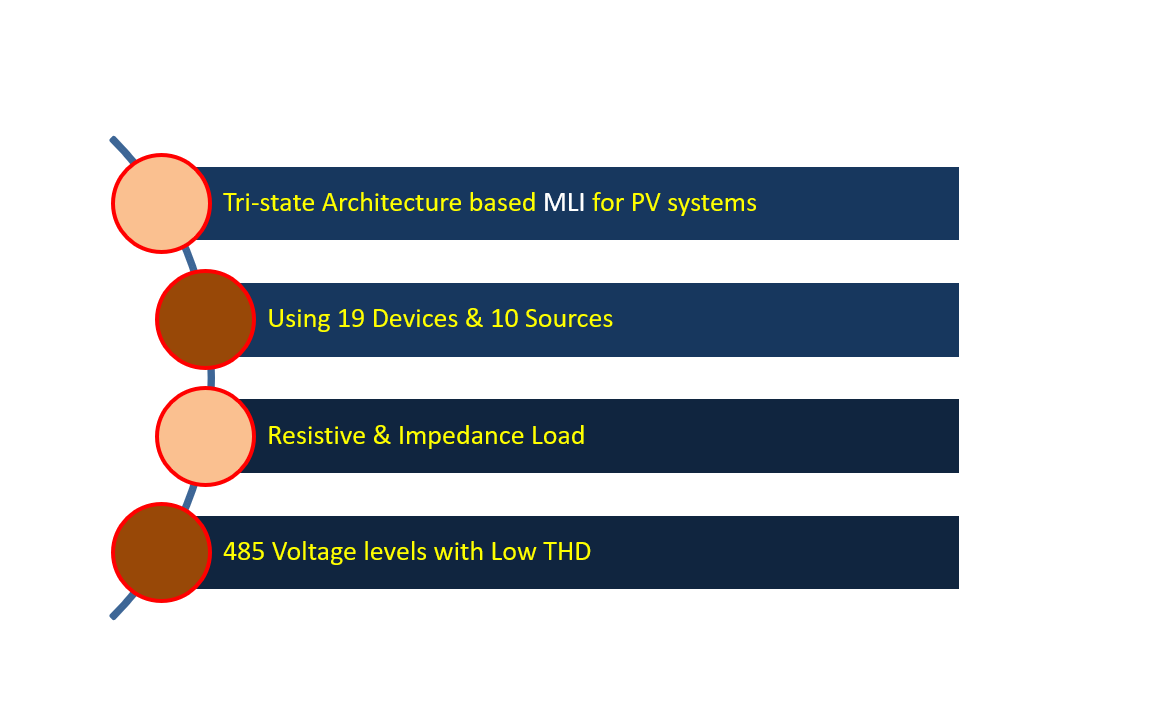
Realization of 485 Level Inverter Using Tri-State Architecture for Renewable Energy Systems


Abstract

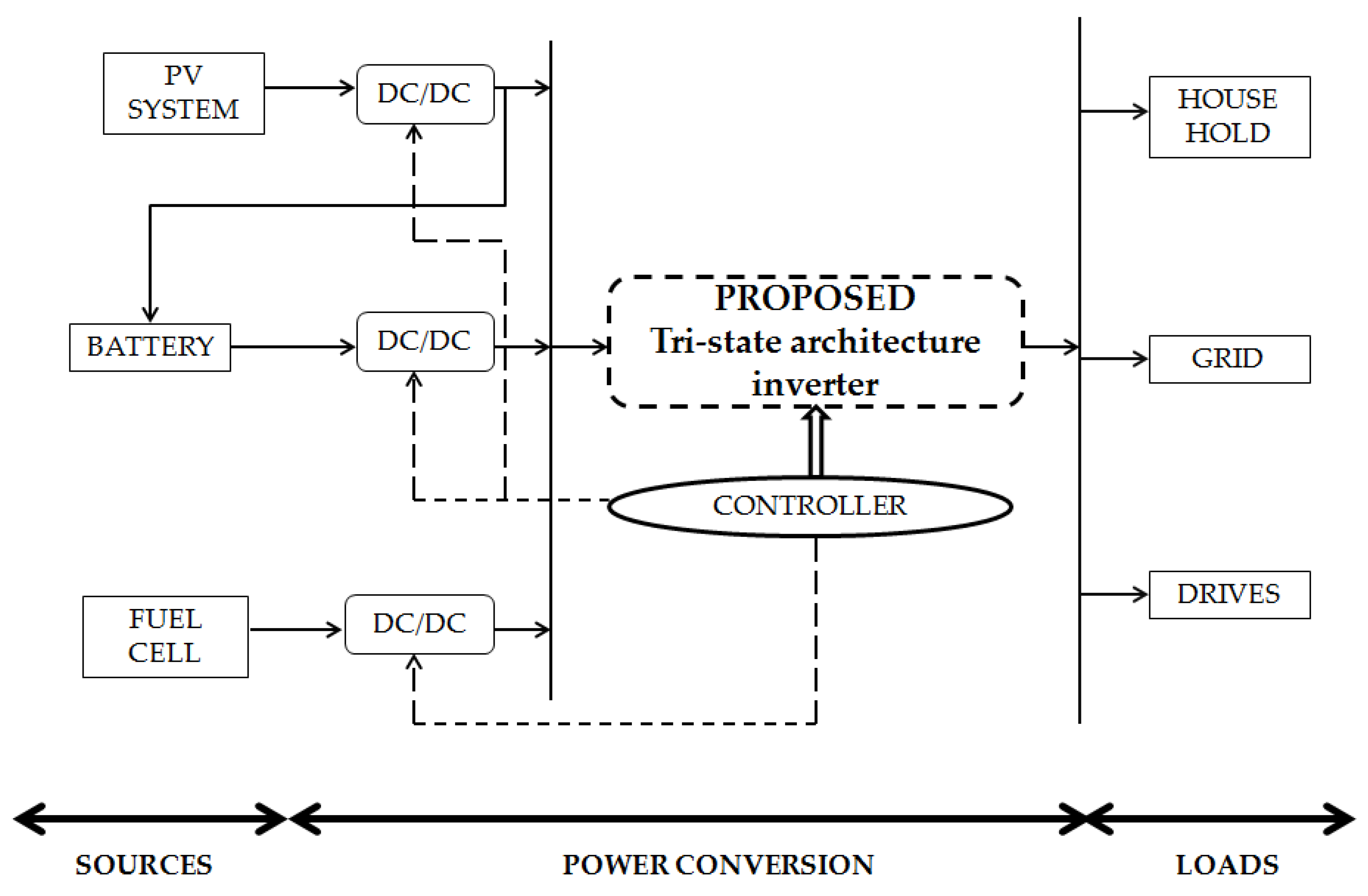
1. Introduction
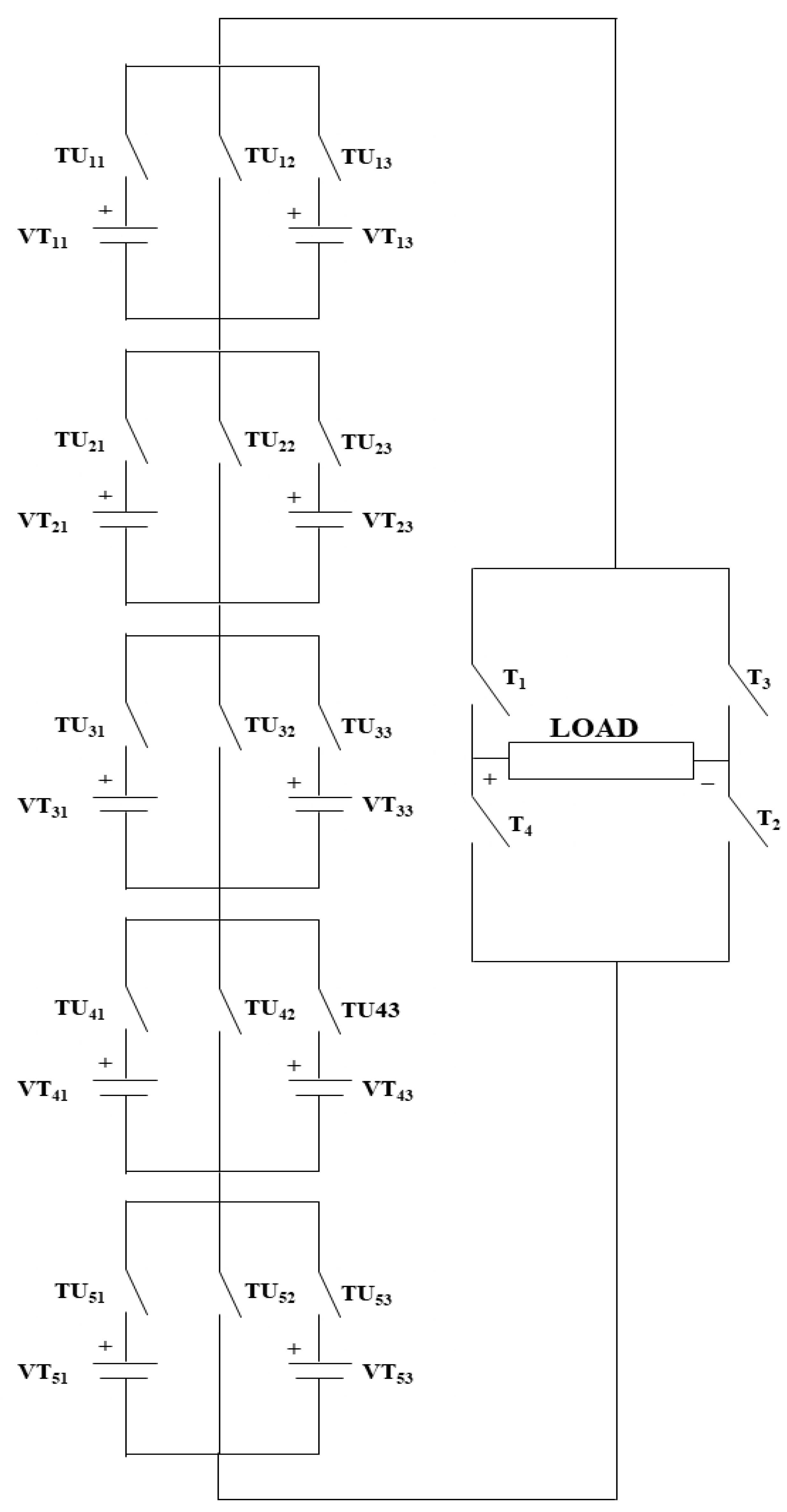
2. Development of 485 Level Inverter Using Tri-State Architecture
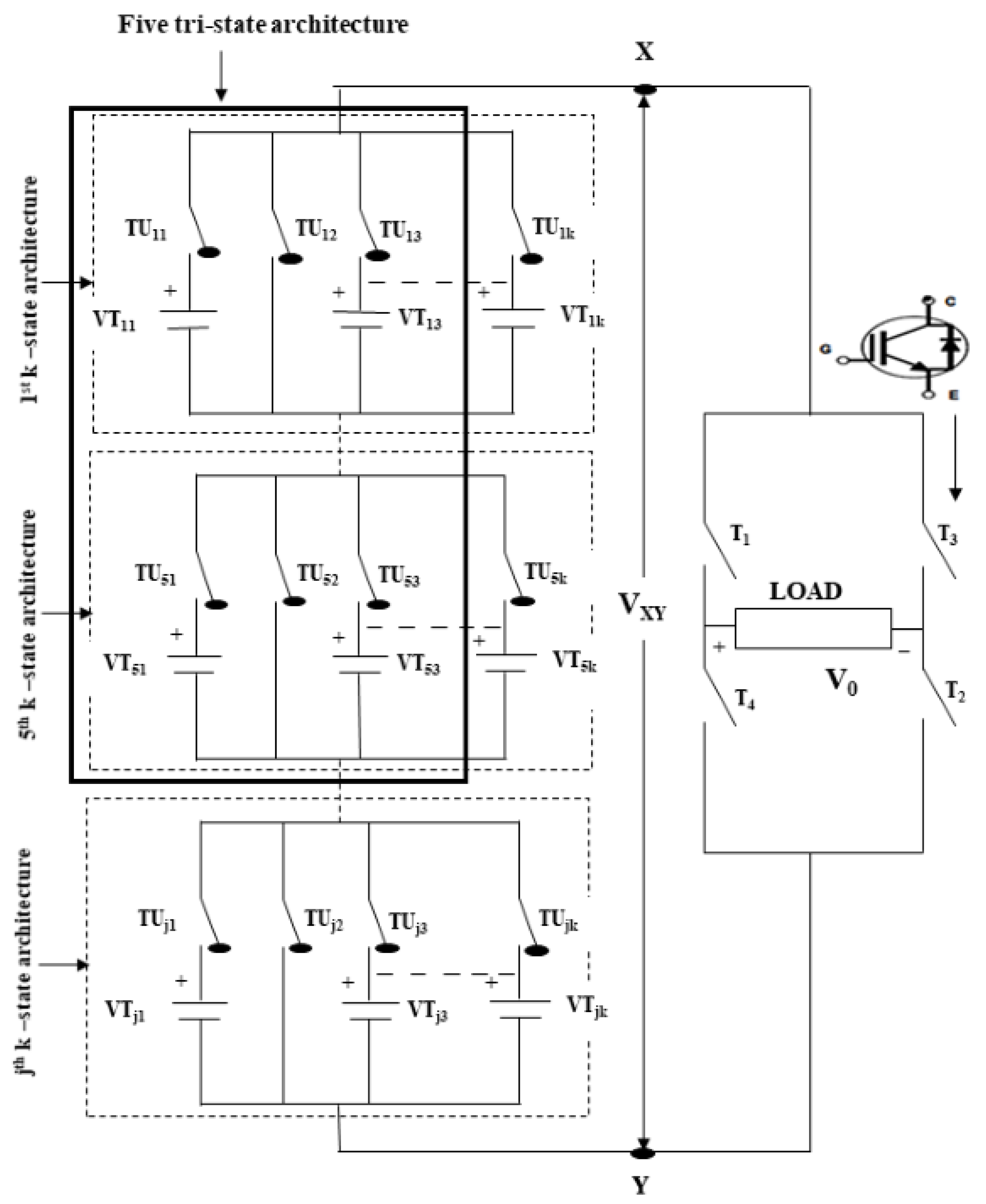
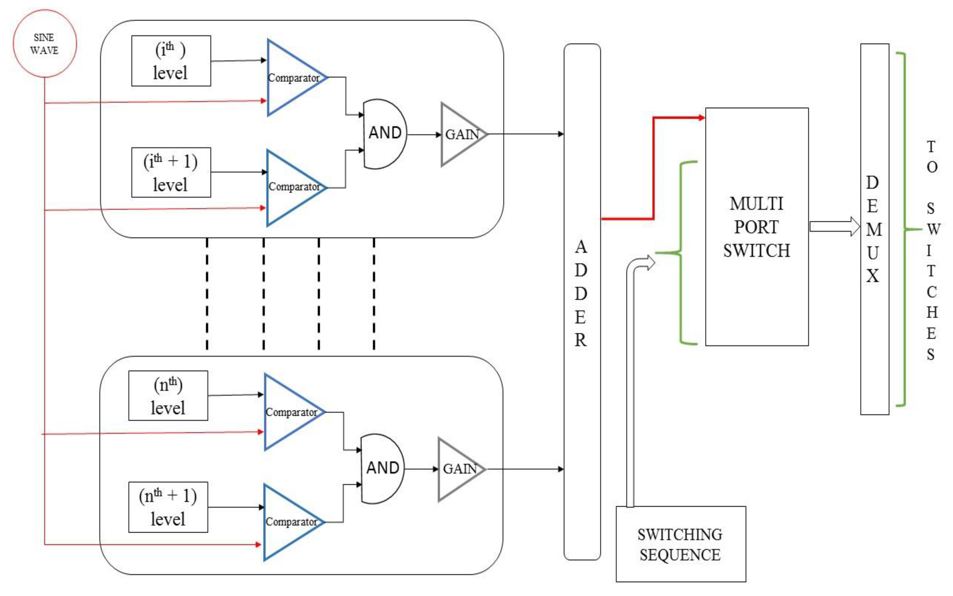
2.1. Working of k-State Inverter
2.2. Development and Design of Tri-State Architecture Based Inverter
- i.
- Smooth step variation in the output so that waveform is sinusoidal.
- ii.
- Capable of generating more voltage levels.
- iii.
- Redundancy is avoided in the levels of voltages.
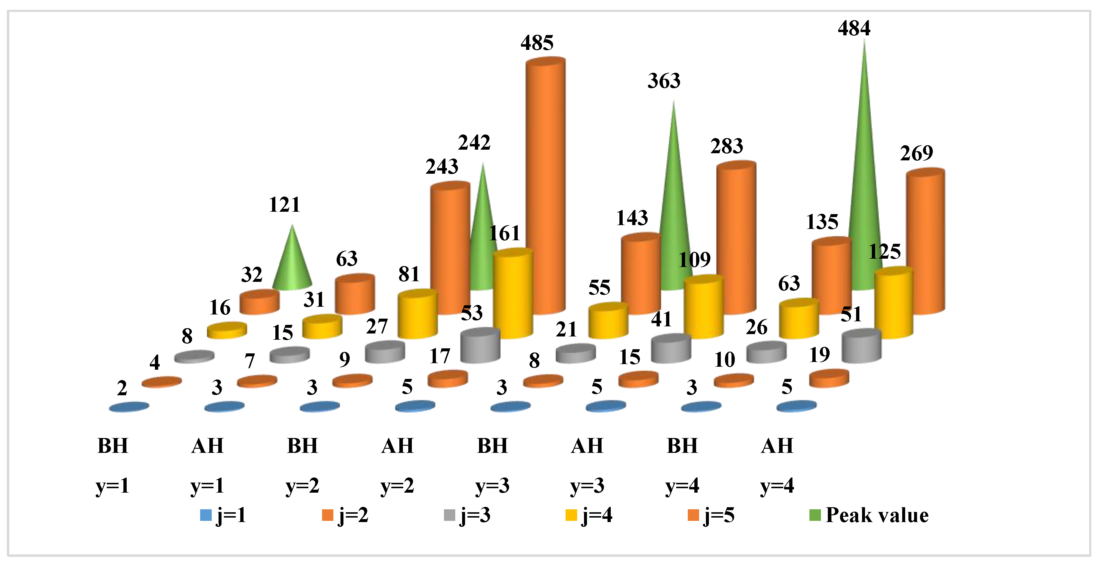
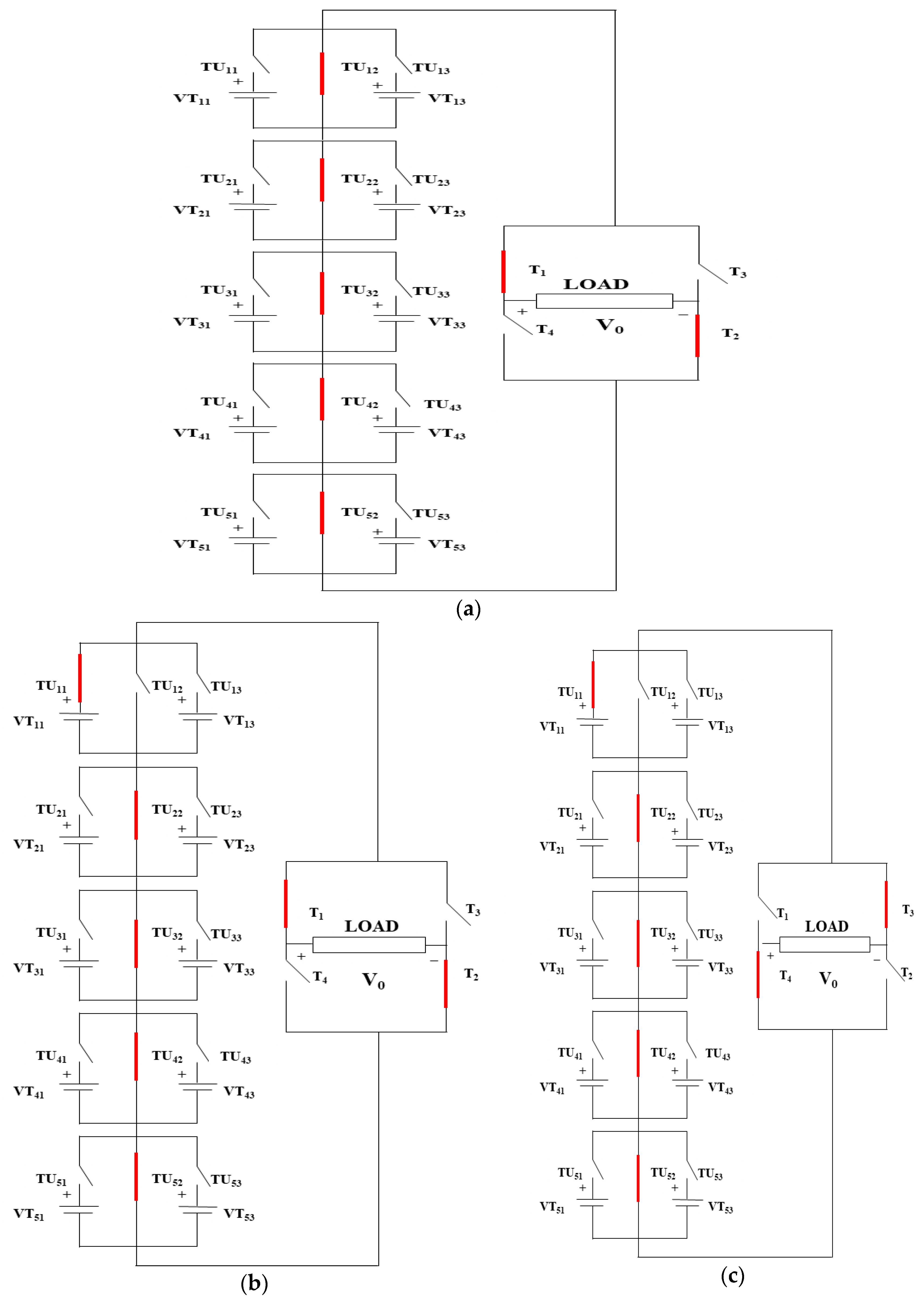
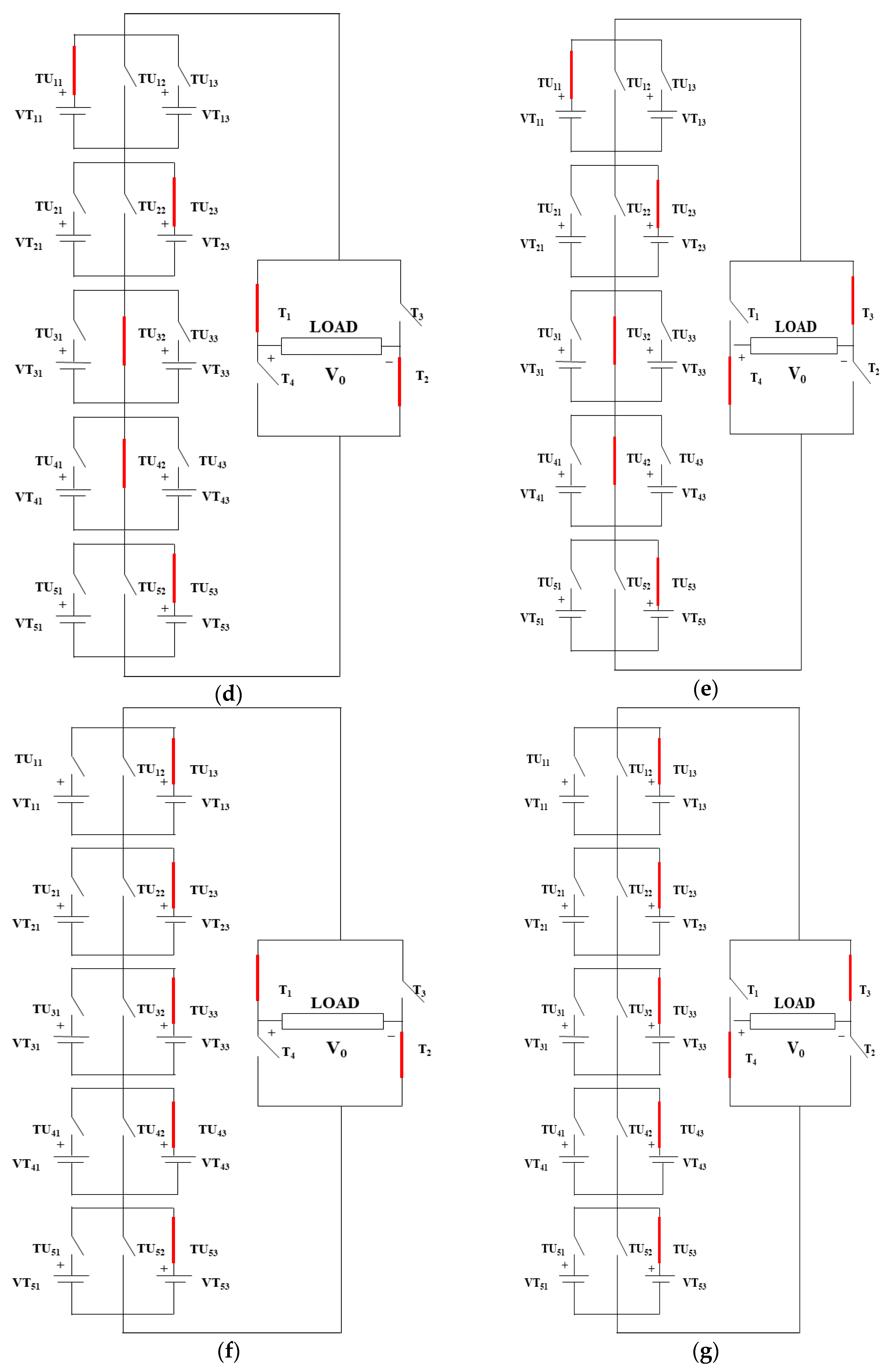
2.3. Development of 485 Level Tri-State Inverter
- Step 1:
- Calculate (169)3, and it is obtained as 20021.
- Step 2:
- From the value 20021, suitable voltage sources and switches are identified, shown in Table 4.
- Stage 1 to generate ‘0’ Volt:
- Stage 2 to generate ‘+1’ Volt/‘−1’ Volt:
- Stage 170 to generate ‘+169’ Volt/‘−169’ Volt:
- Stage 243 to generate ‘+242’ Volt/‘−242’ Volt:
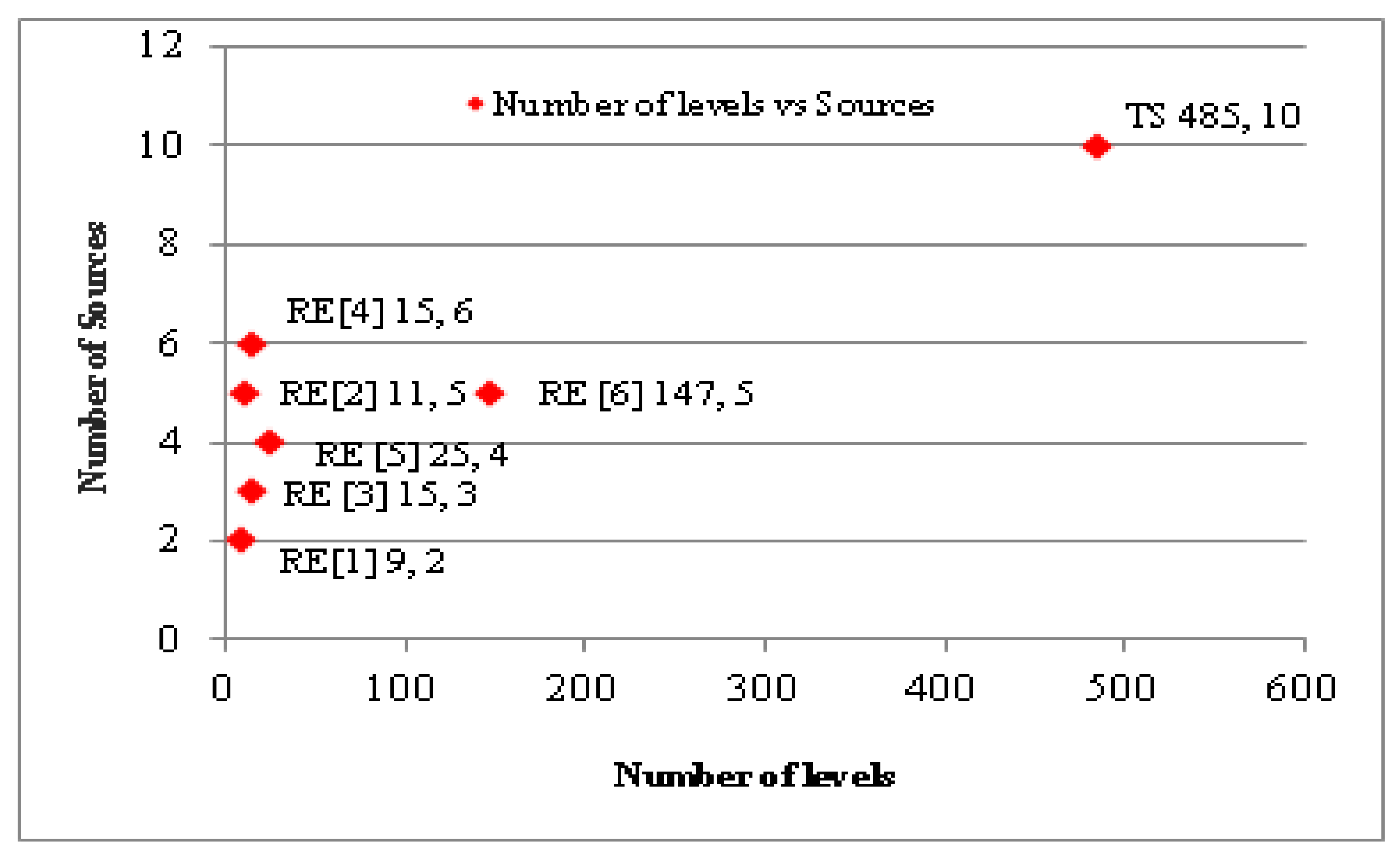
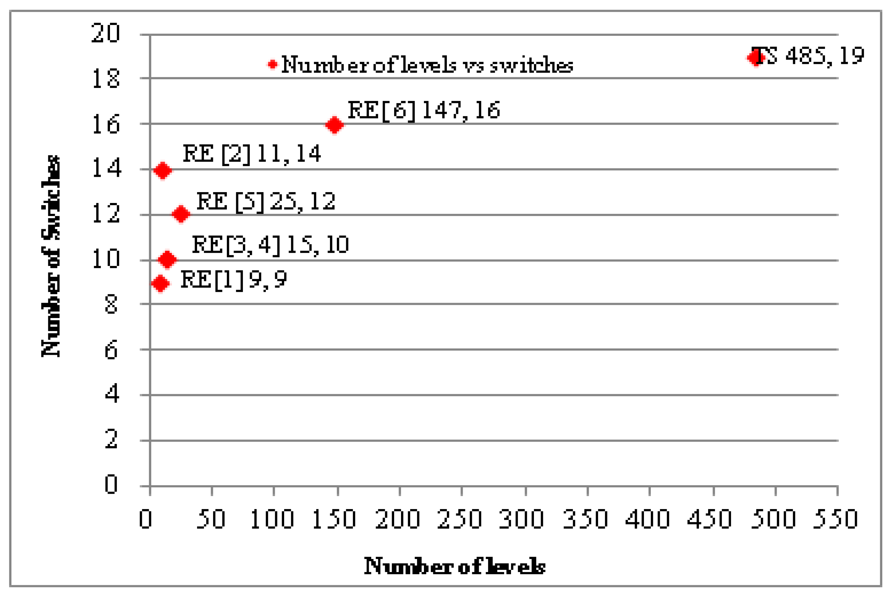
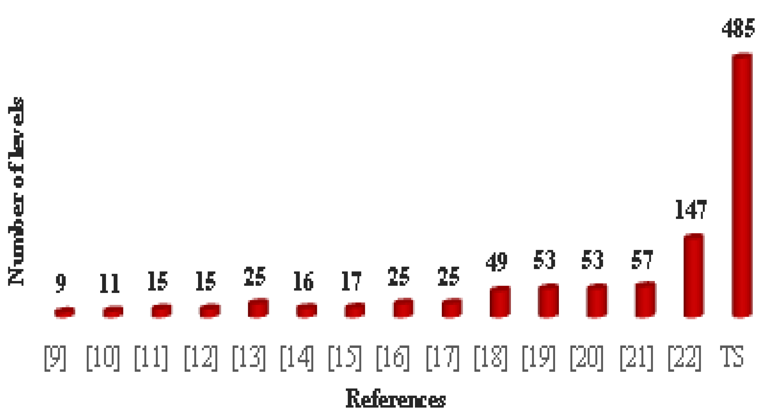
2.4. Comparative Study of Existing MLI Designs with the Proposed Inverter Structure
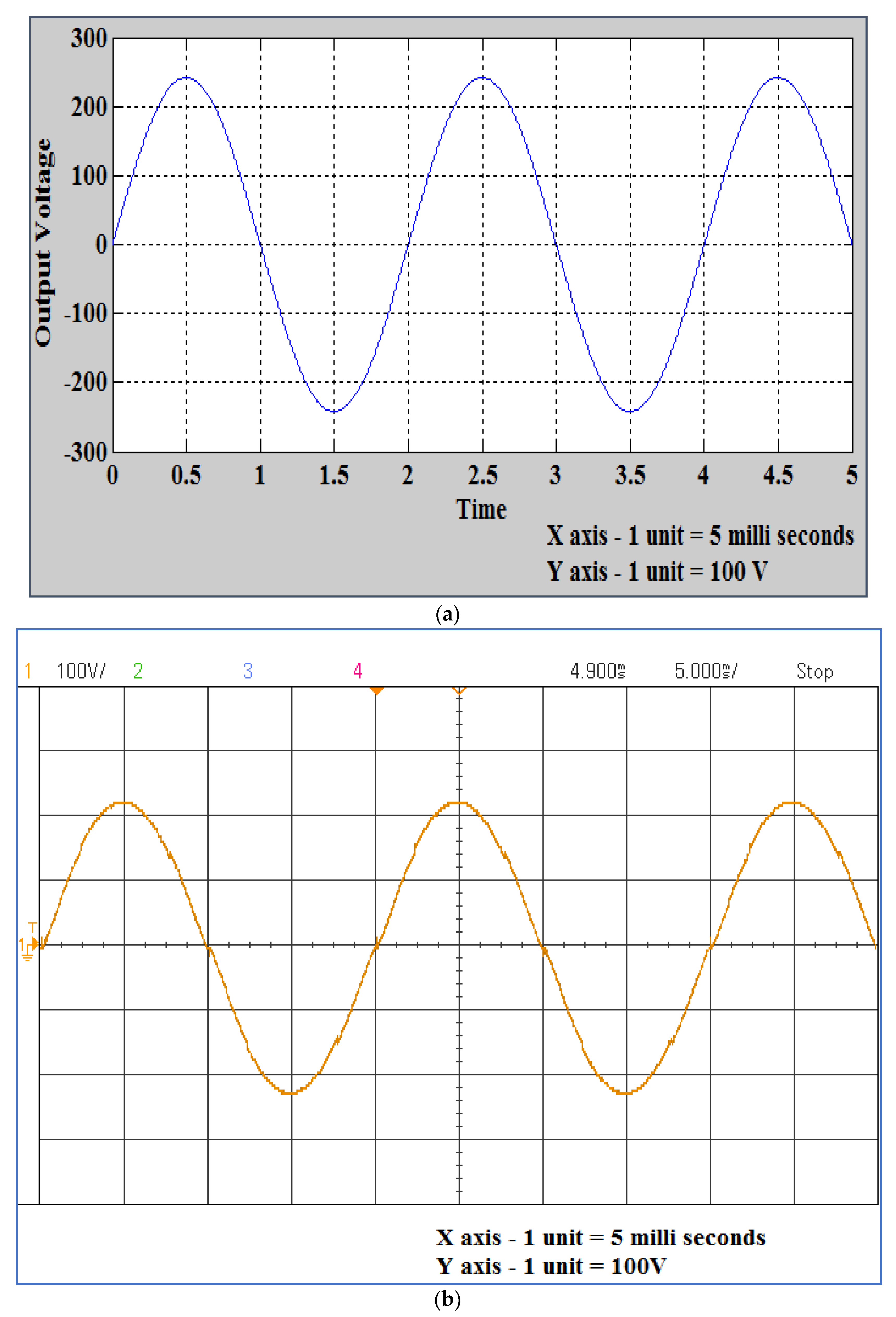
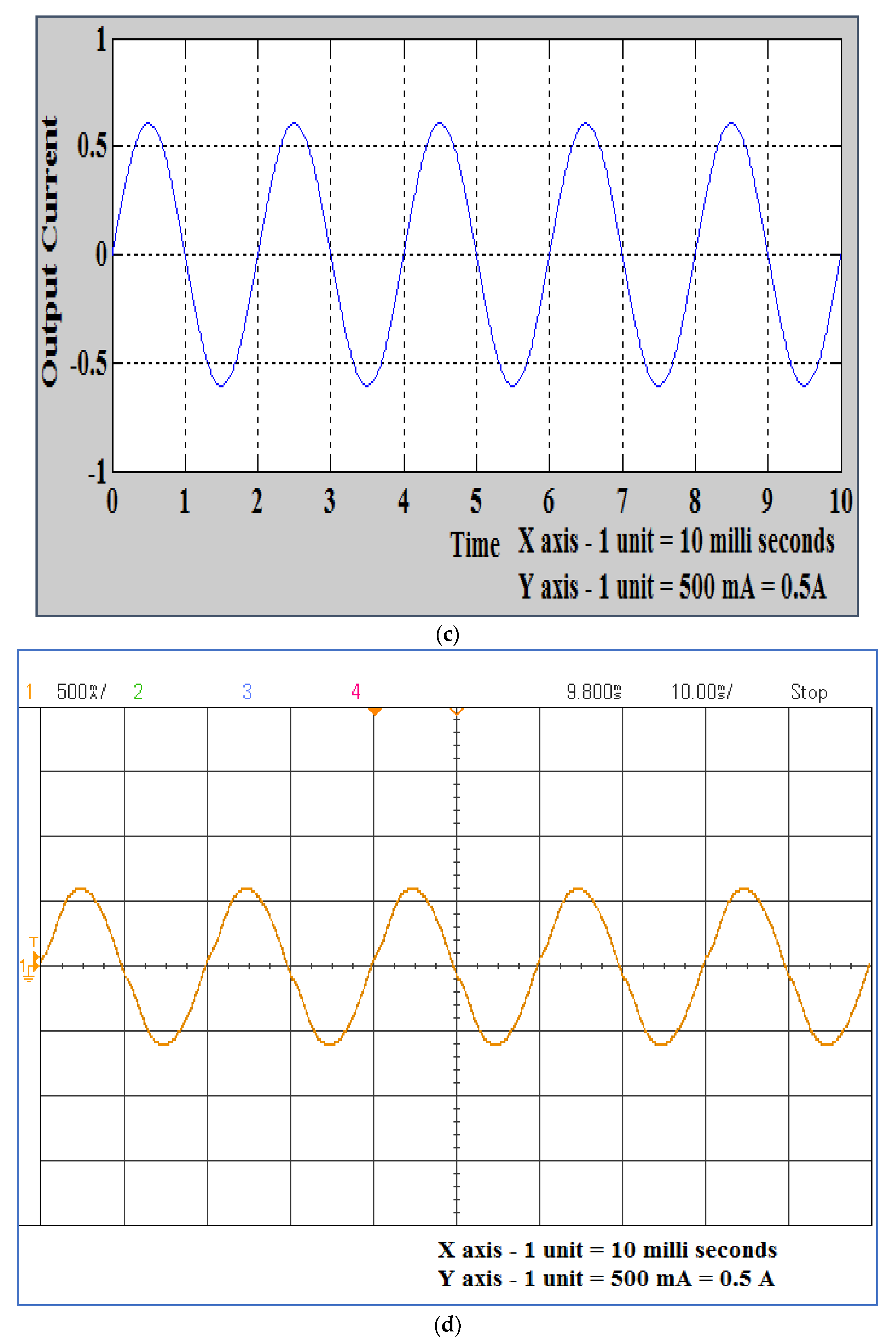
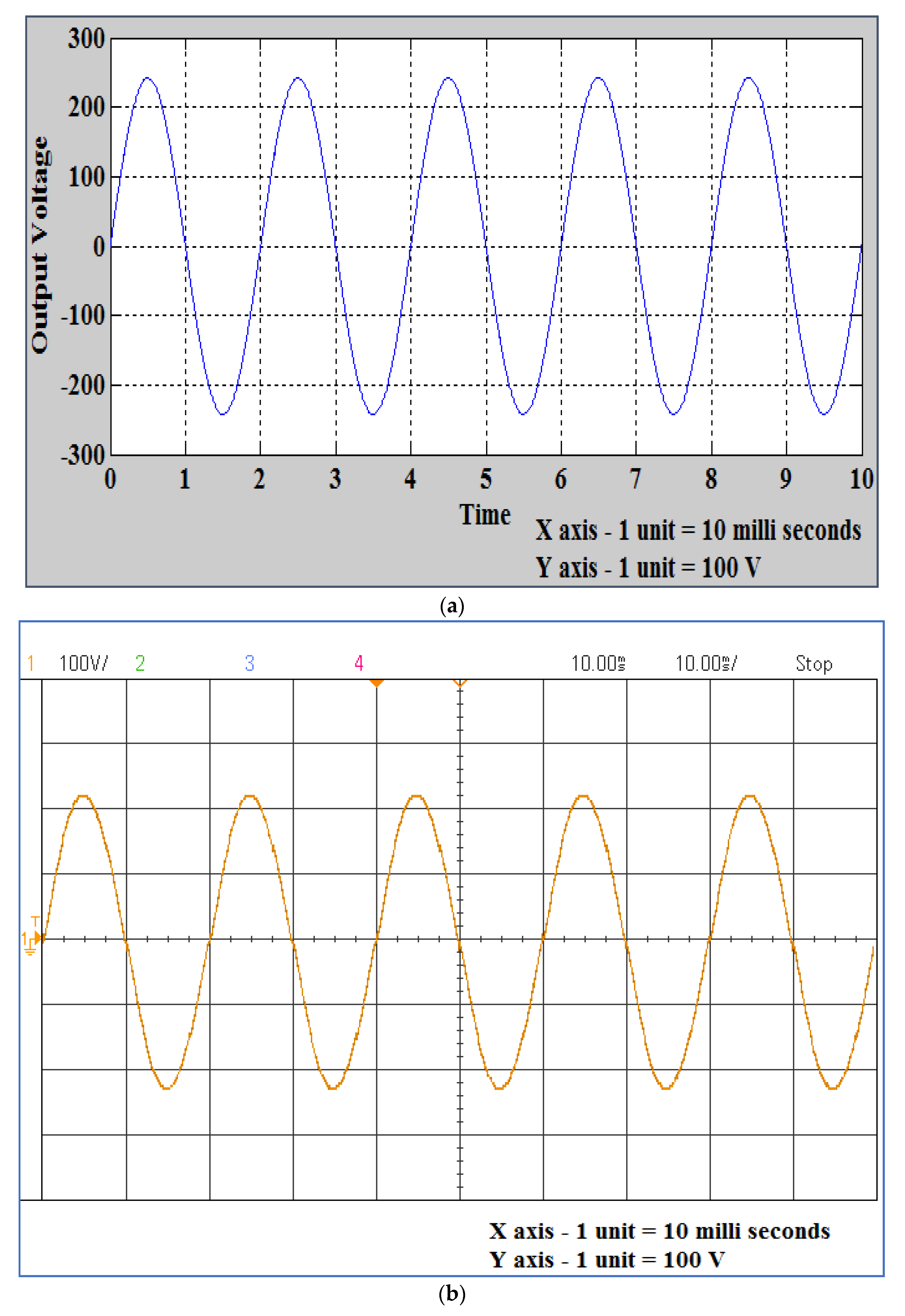
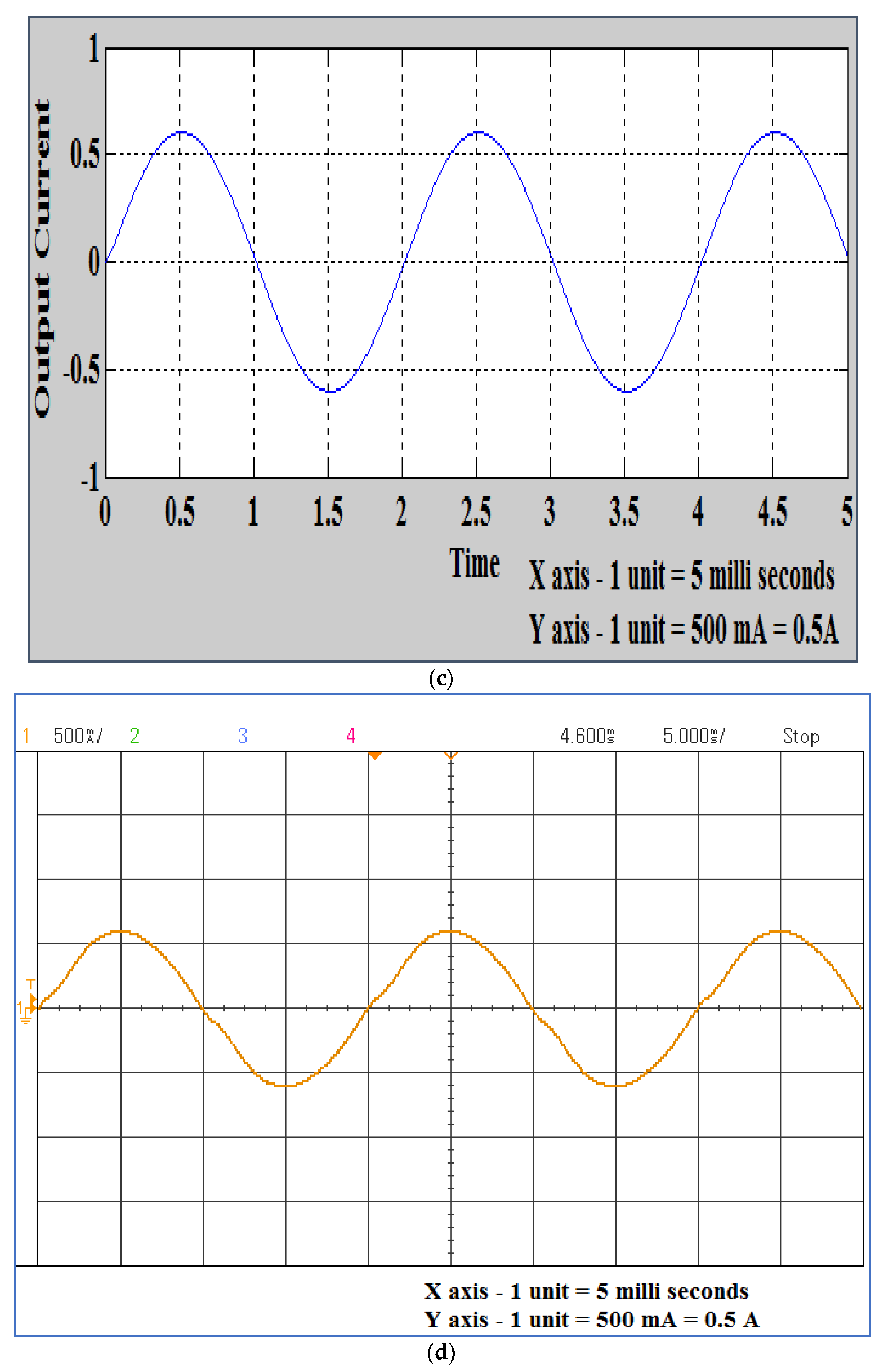
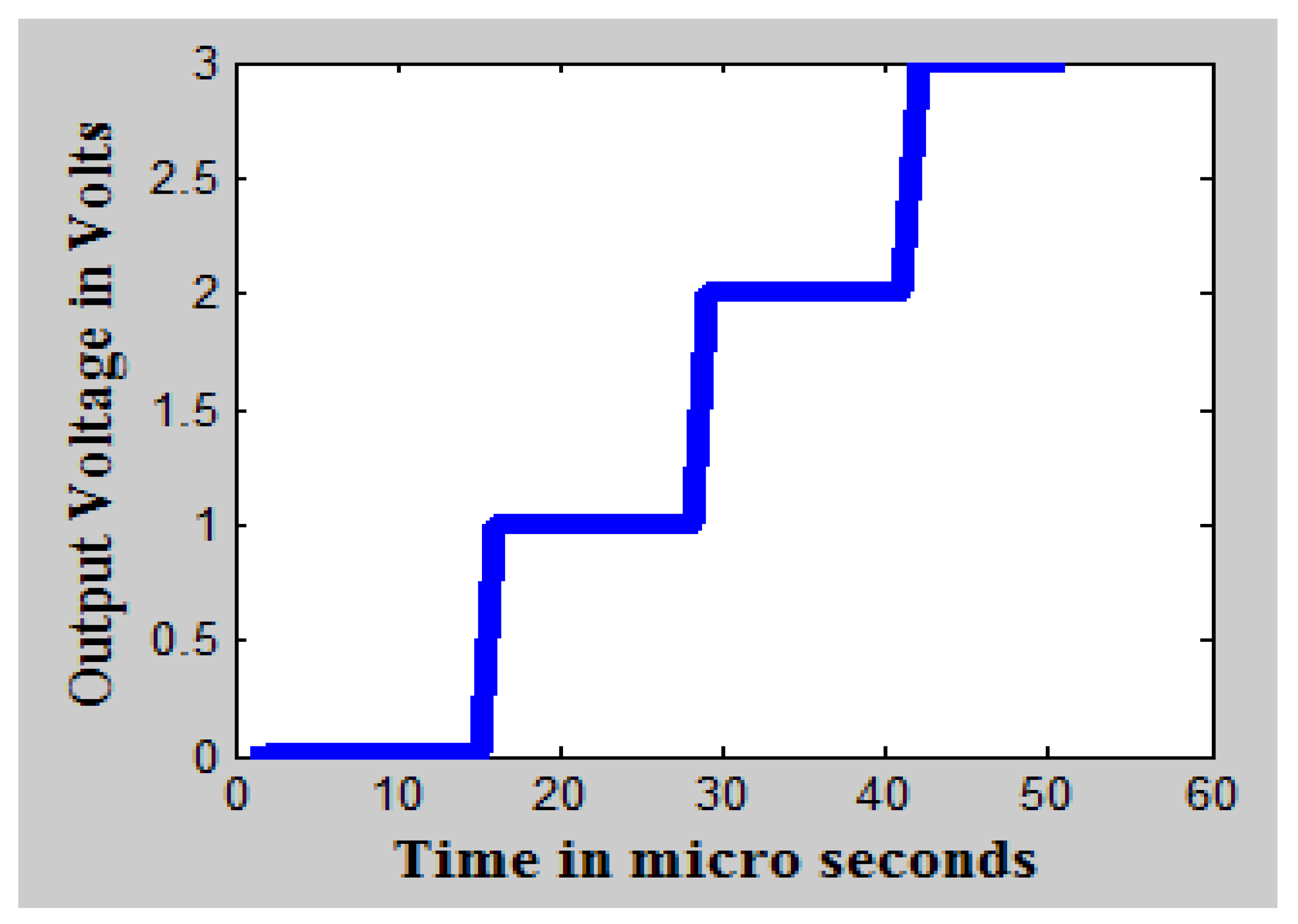
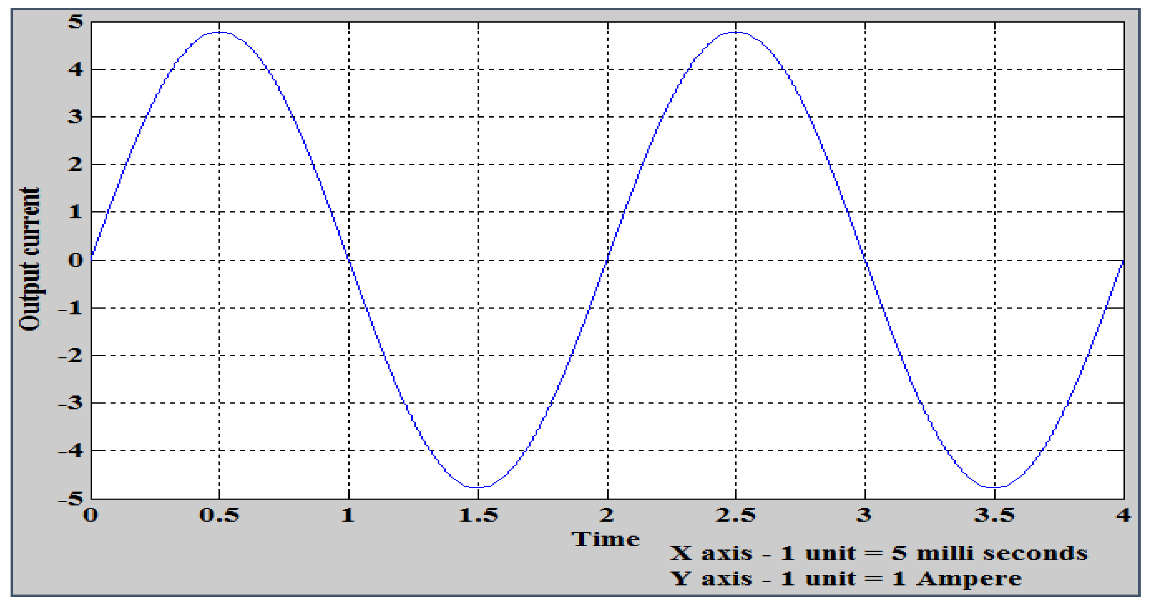
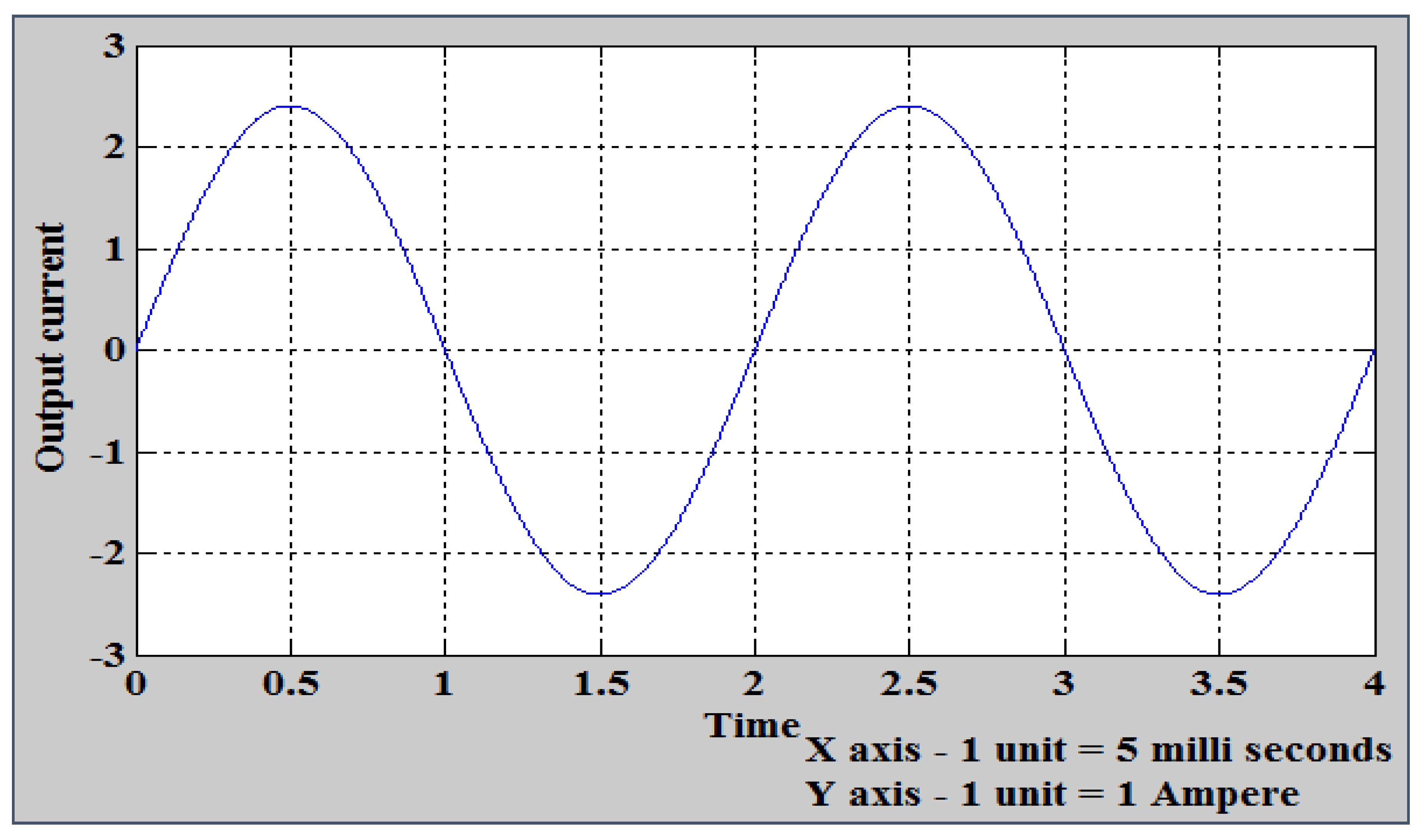
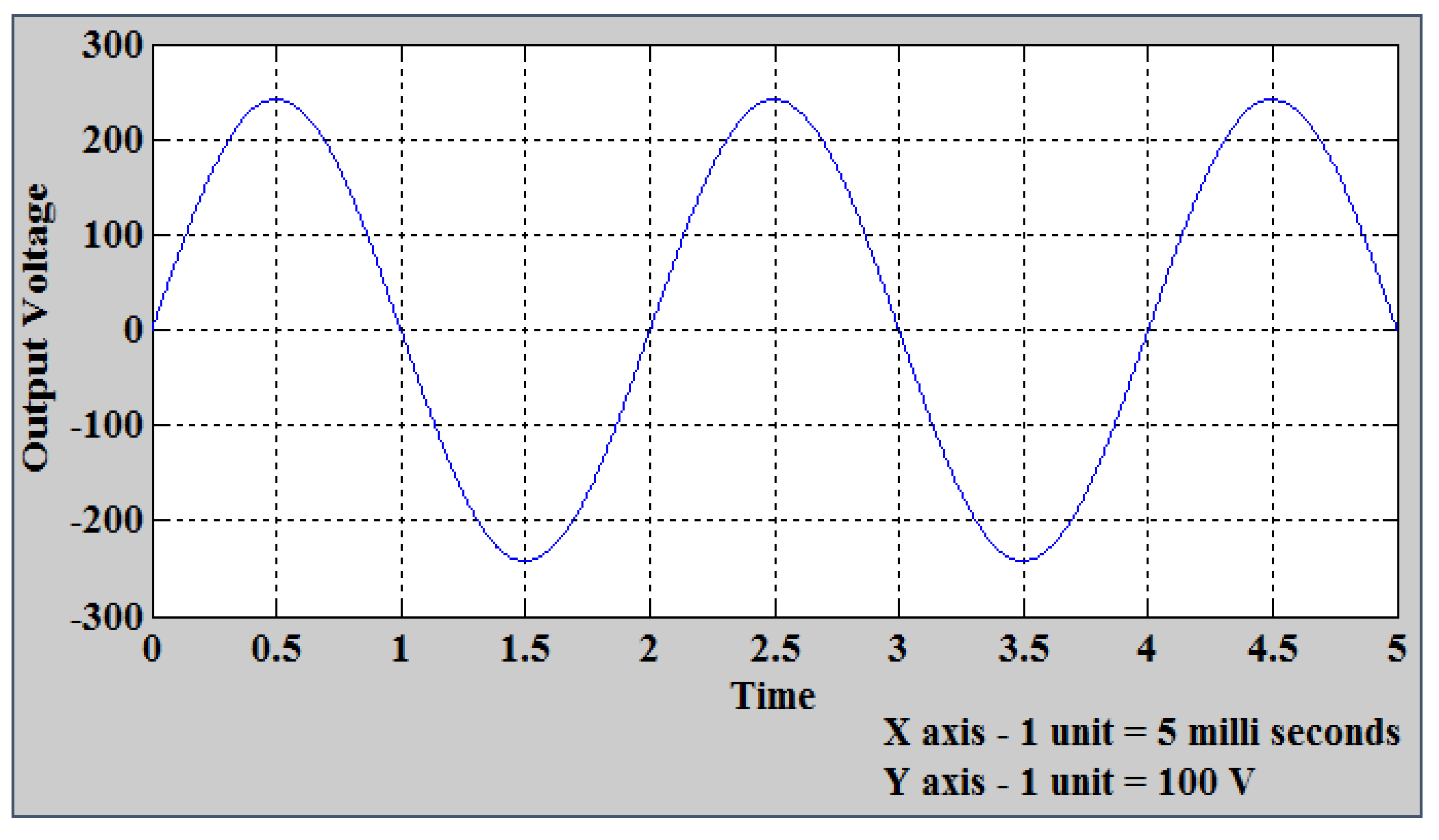
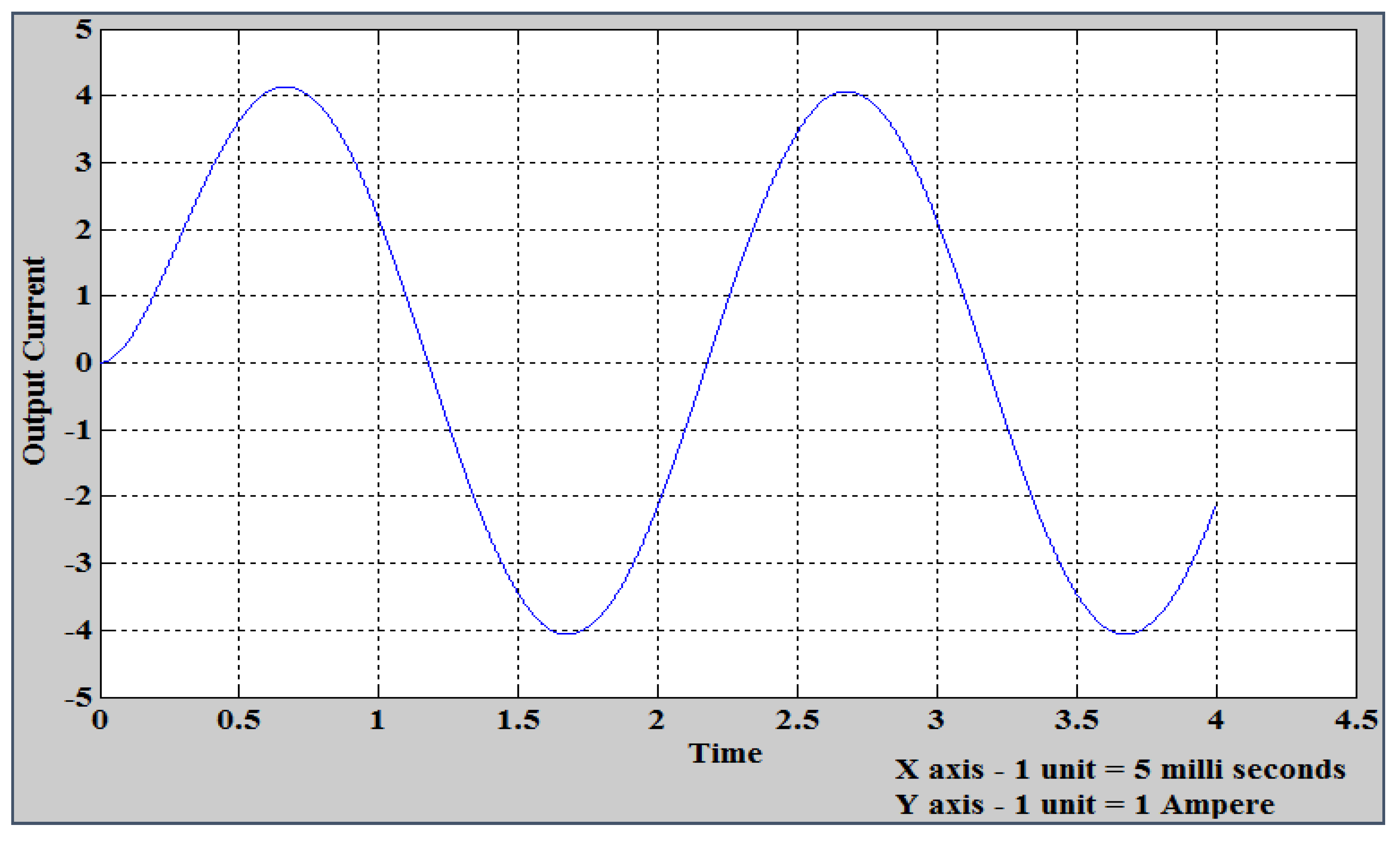
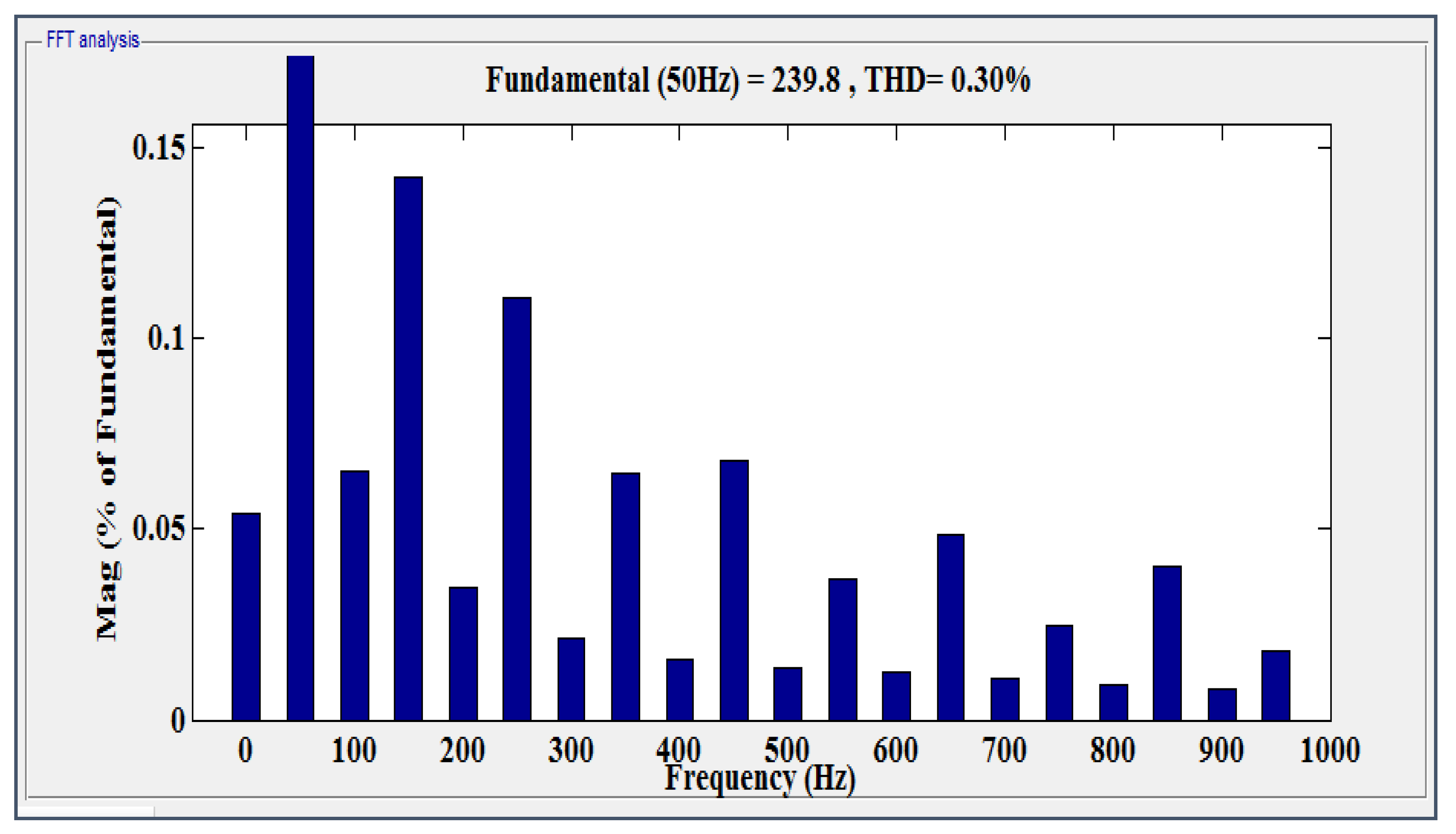
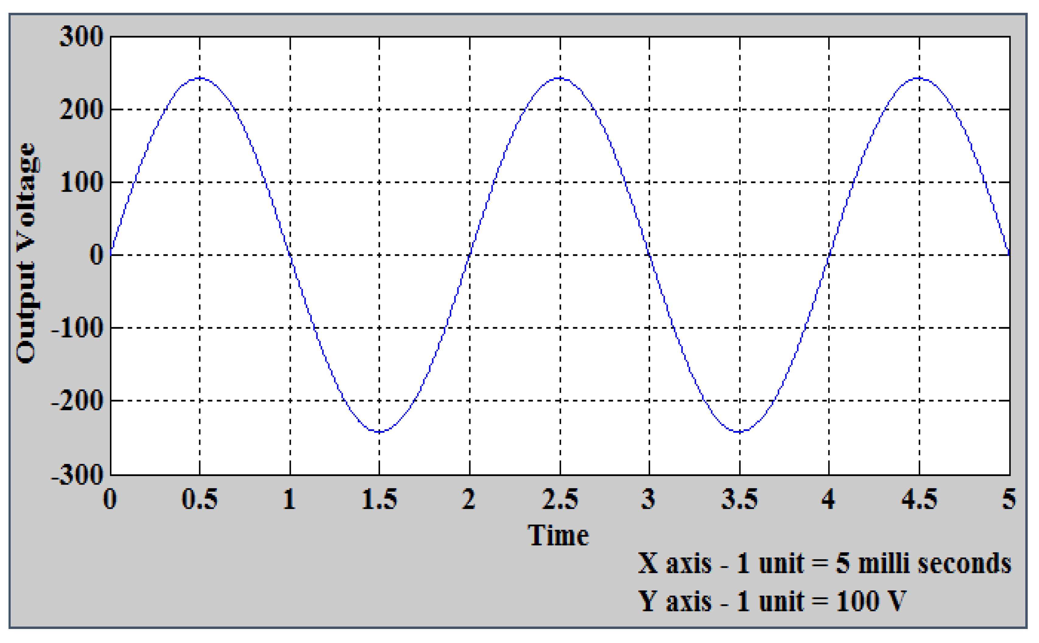
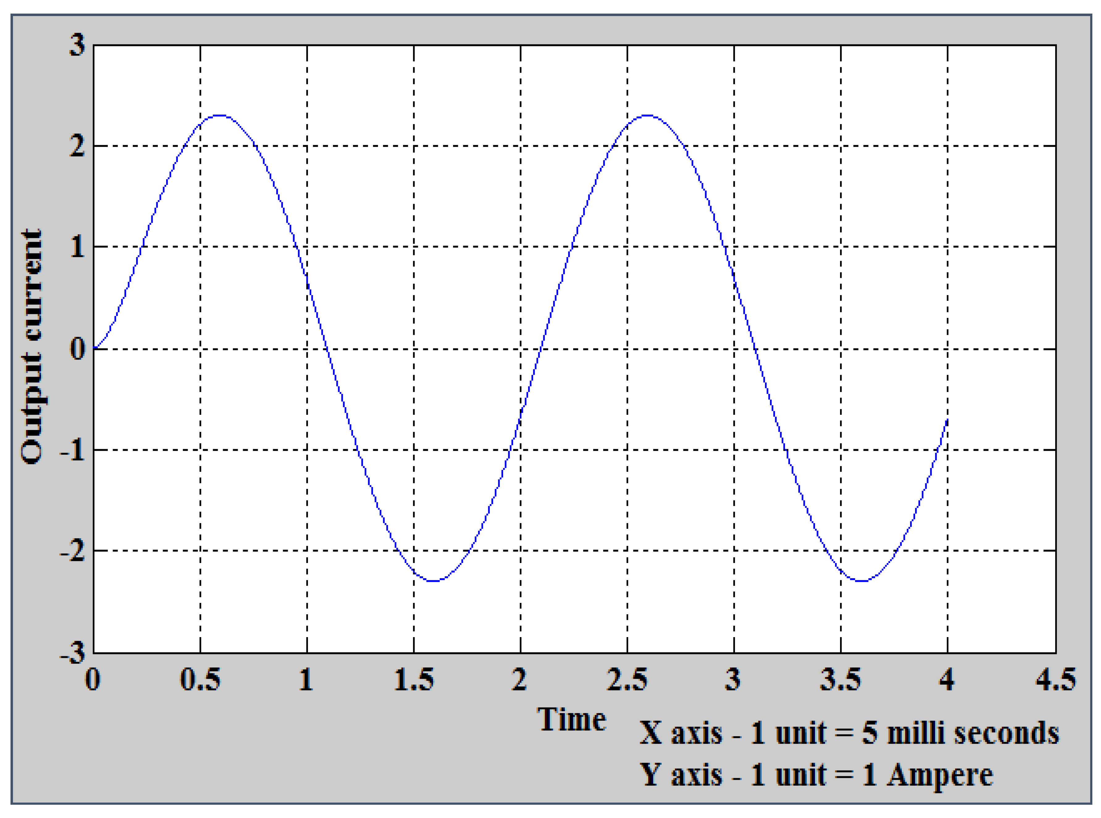
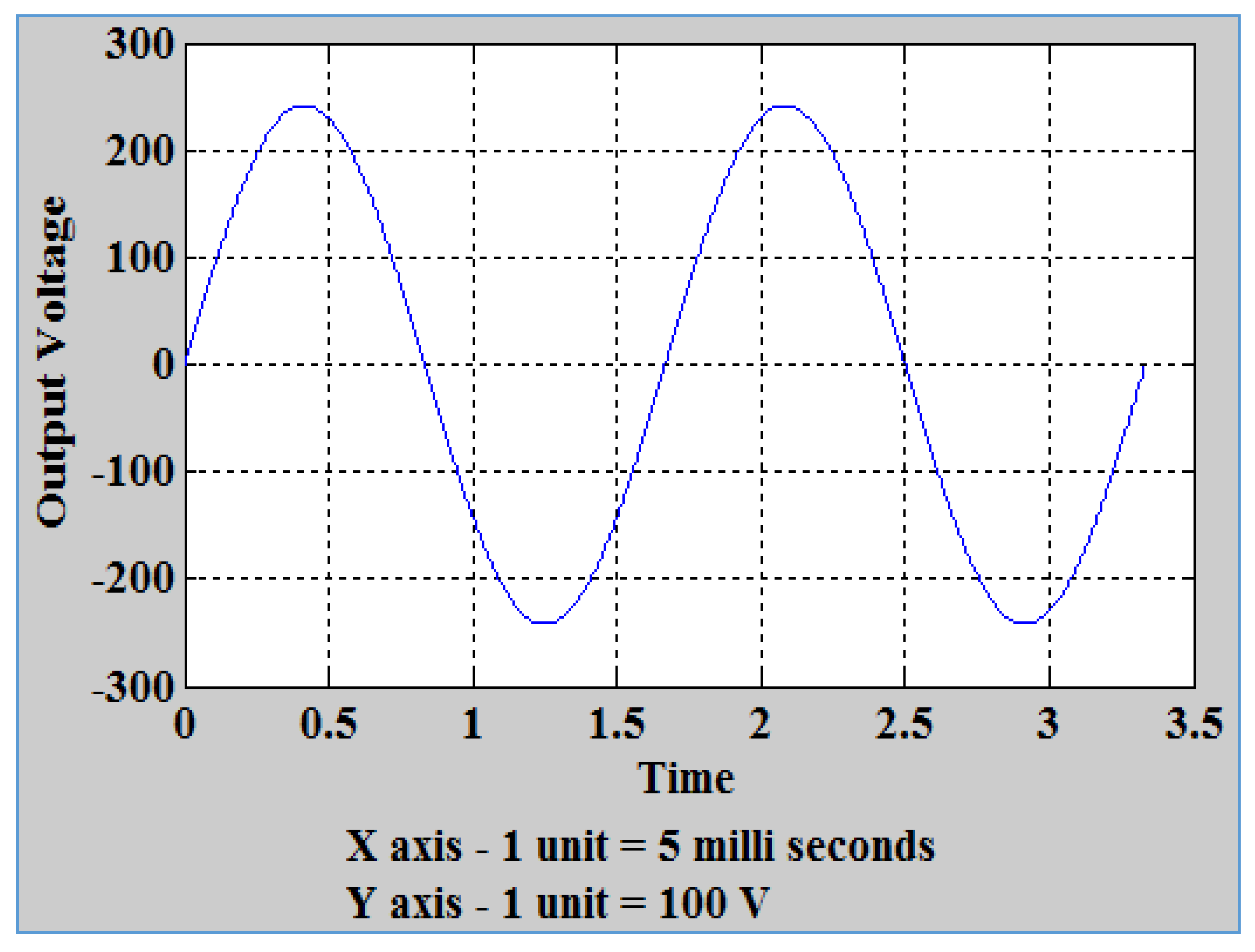
3. Simulation and Experimentation of Tri-State Inverter
3.1. A Systematic Approach in Designing the Experimentation of Tri-State Inverter
3.2. Safe Operation of Proposed Tri-State Inverter
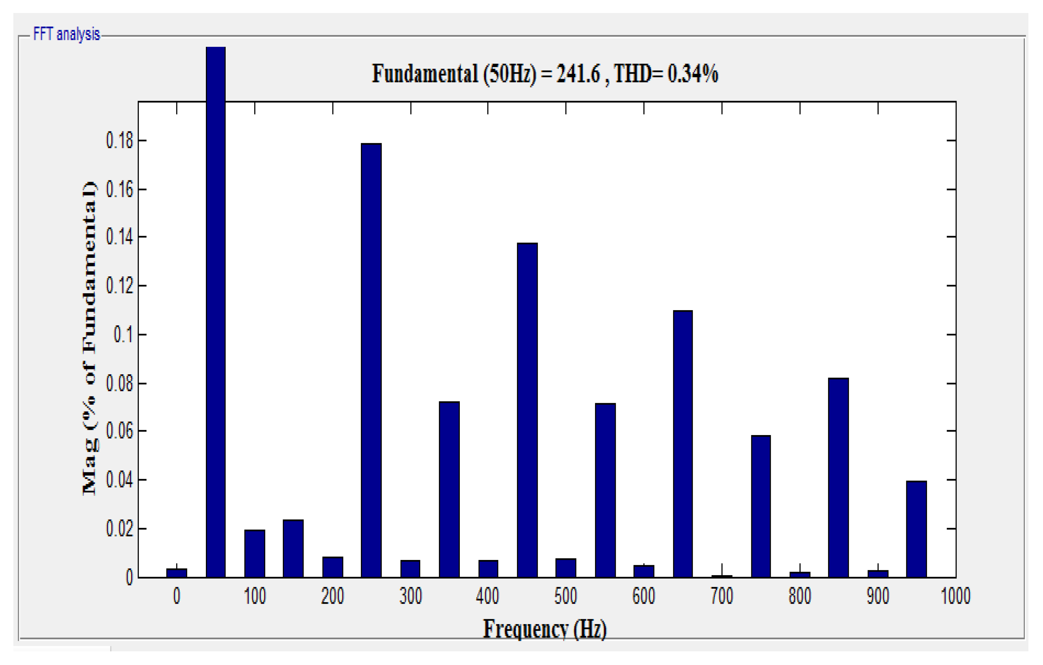
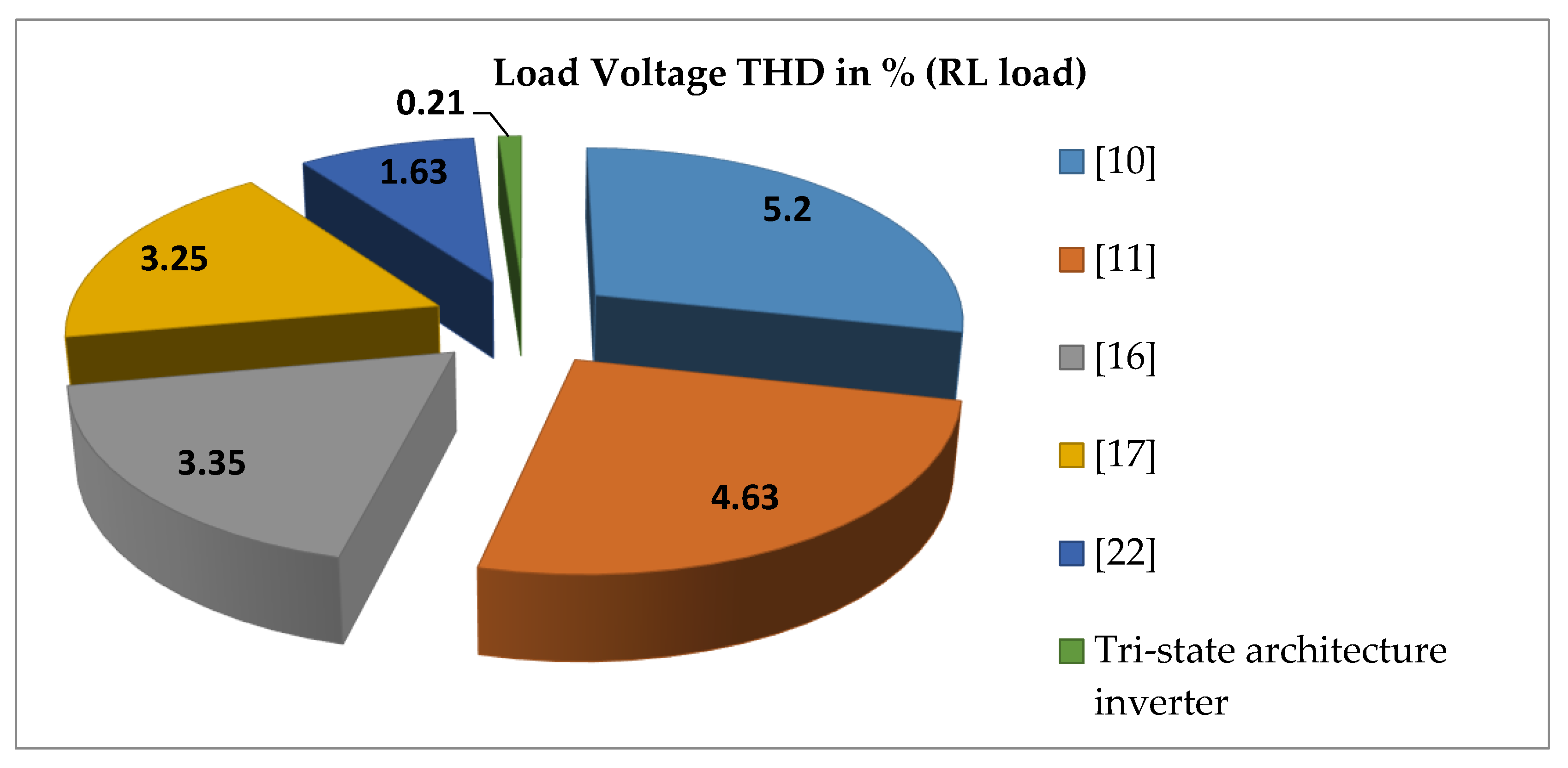
3.3. Validation of Tri-State Inverter Results with Other MLI’s
4. Conclusions
Author Contributions
Funding
Conflicts of Interest
References
- Roemer, F.; Ahmad, M.; Chang, F.; Lienkamp, M. Optimization of a Cascaded H-Bridge Inverter for Electric Vehicle Applications Including Cost Consideration. Energies 2019, 12, 4272. [Google Scholar] [CrossRef]
- Karthikeyan, D.; Vijayakumar, K.; Jagabar Sathik, M. Generalized Cascaded Symmetric and Level Doubling Multilevel Converter Topology with Reduced THD for Photovoltaic Applications. Electronics 2019, 8, 161. [Google Scholar]
- Samadaei, E.; Salehi, A.; Iranian, M.; Pouresmaeil, E. Single DC Source Multilevel Inverter with Changeable Gains and Levels for Low-Power Loads. Electronics 2020, 9, 937. [Google Scholar] [CrossRef]
- Zeng, X.; Gong, D.; Wei, M.; Xie, J. Research on novel hybrid multilevel inverter with cascaded H-bridges at alternating current side for high-voltage direct current transmission. IET Power Electron. 2018, 11, 1914–1925. [Google Scholar] [CrossRef]
- Sunddararaj, S.P.; Srinivasarangan Rangarajan, S.; Subashini, N. An Extensive Review of Multilevel Inverters Based on Their Multifaceted Structural Configuration, Triggering Methods and Applications. Electronics 2020, 9, 433. [Google Scholar] [CrossRef]
- Vijayaraja, L.; Kumar, S.G.; Rivera, M. A review on multilevel inverter with reduced switch count. In Proceedings of the 2016 IEEE International Conference on Automatica (ICA-ACCA), Curico, Chile, 19–21 October 2016; pp. 1–5. [Google Scholar]
- Ahmad, A.; Anas, M.; Sarwar, A.; Zaid, M.; Tariq, M.; Ahmad, J.; Beig, A.R. Realization of a Generalized Switched-Capacitor Multilevel Inverter Topology with Less Switch Requirement. Energies 2020, 13, 1556. [Google Scholar] [CrossRef]
- Ganesh, B.; Murugan, N.; Nallaswamy, M.; Rajkumar, K.; Vijayaraja, L.; Kumar, S.G.; Rivera, M. Implementation of Twenty seven level and Fifty one level Inverter using constant voltage sources. In Proceedings of the 2019 IEEE CHILEAN Conference on Electrical, Electronics Engineering, Information and Communication Technologies (CHILECON), Valparaiso, Chile, 13–27 November 2019; pp. 1–4. [Google Scholar]
- Prabaharan, N.; Salam, Z.; Cecati, C.; Palanisamy, K. Design and Implementation of New Multilevel Inverter Topology for Trinary Sequence Using Unipolar Pulsewidth Modulation. IEEE Trans. Ind. Electron. 2020, 67, 3573–3582. [Google Scholar] [CrossRef]
- Babaei, E.; Hosseini, S.H. New cascaded multilevel inverter topology with minimum number of switches. Energy Convers. Manag. 2009, 50, 2761–2767. [Google Scholar] [CrossRef]
- Babaei, E.; Kangarlu, M.F.; Mazgar, F.N. Symmetric and asymmetric multilevel inverter topologies with reduced switching devices. Electr. Power Syst. Res. 2012, 86, 122–130. [Google Scholar] [CrossRef]
- Avanaki, H.N.; Barzegarkhoo, R.; Zamiri, E.; Yang, Y.; Blaabjerg, F. Reduced switch-count structure for symmetric multilevel inverters with a novel switched-DC-source submodule. IET Power Electron. 2019, 12, 311–321. [Google Scholar] [CrossRef]
- Siddique, M.D.; Mekhilef, S.; Shah, N.M.; Sarwar, A.; Iqbal, A.; Memon, M.A. A New Multilevel Inverter Topology With Reduce Switch Count. IEEE Access 2019, 7, 58584–58594. [Google Scholar] [CrossRef]
- Shahir, F.M.; Babaei, E. 16-level basic topology for cascaded multilevel inverters with reduced number of components. In Proceedings of the IECON 2016—42nd Annual Conference of the IEEE Industrial Electronics Society, Florence, Italy, 23–26 October 2016; pp. 3105–3110. [Google Scholar]
- Sarbanzadeh, M.; Babaei, E.; Hosseinzadeh, M.A.; Cecati, C. A new sub-multilevel inverter with reduced number of components. In Proceedings of the IECON 2016—42nd Annual Conference of the IEEE Industrial Electronics Society, Florence, Italy, 23–26 October 2016; pp. 3166–3171. [Google Scholar]
- Alishah, R.S.; Nazarpour, D.; Hosseini, S.H.; Sabahi, M. Reduction of Power Electronic Elements in Multilevel Converters Using a New Cascade Structure. IEEE Trans. Ind. Electron. 2015, 62, 256–269. [Google Scholar] [CrossRef]
- Babaei, E.; Gowgani, S.S. Hybrid Multilevel Inverter Using Switched Capacitor Units. IEEE Trans. Ind. Electron. 2014, 61, 4614–4621. [Google Scholar] [CrossRef]
- Babaei, E.; Laali, S.; Alilu, S. Cascaded Multilevel Inverter with Series Connection of Novel H-Bridge Basic Units. IEEE Trans. Ind. Electron. 2014, 61, 6664–6671. [Google Scholar] [CrossRef]
- Babaei, E. A Cascade Multilevel Converter Topology with Reduced Number of Switches. IEEE Trans. Power Electron. 2008, 23, 2657–2664. [Google Scholar] [CrossRef]
- Vijayaraja, L.; Kumar, S.G.; Rivera, M. A New Topology of Multilevel Inverter with Reduced Part Count. In Proceedings of the 2018 IEEE International Conference on Automation/XXIII Congress of the Chilean Association of Automatic Control (ICA-ACCA), Concepcion, Chile, 17–19 October 2018; pp. 1–5. [Google Scholar]
- Boora, K.; Kumar, J. A Novel Cascaded Asymmetrical Multilevel Inverter with Reduced Number of Switches. IEEE Trans. Ind. Appl. 2019, 55, 7389–7399. [Google Scholar] [CrossRef]
- Babadi, A.N.; Salari, O.; Mojibian, M.J.; Bina, M.T. Modified Multilevel Inverters With Reduced Structures Based on PackedU-Cell. IEEE J. Emerg. Sel. Top. Power Electron. 2018, 6, 874–887. [Google Scholar] [CrossRef]
- Chappa, A.; Gupta, S.; Sahu, L.K.; Gautam, S.P.; Gupta, K.K. Symmetrical and Asymmetrical Reduced Device Multilevel Inverter Topology. IEEE J. Emerg. Sel. Top. Power Electron. 2019. accepted. [Google Scholar] [CrossRef]
- Gautam, S.P. Novel H-Bridge-Based Topology of Multilevel Inverter with Reduced Number of Devices. IEEE J. Emerg. Sel. Top. Power Electron. 2019, 7, 2323–2332. [Google Scholar] [CrossRef]
- Raman, G.; Imthiyas, A.; Raja, M.D.; Vijayaraja, L.; Kumar, S.G. Design of 31-level Asymmetric Inverter with Optimal Number of Switches. In Proceedings of the 2019 IEEE International Conference on Intelligent Techniques in Control, Optimization and Signal Processing (INCOS), Tamilnadu, India, 11–13 April 2019; pp. 1–3. [Google Scholar]
- Aganah, K.A.; Luciano, C.; Ndoye, M.; Murphy, G. New Switched-Dual-Source Multilevel Inverter for Symmetrical and Asymmetrical Operation. Energies 2018, 11, 984. [Google Scholar] [CrossRef]


| Level Generation (Volts) | Switching Combination | ||||
|---|---|---|---|---|---|
| 0 | TUj1 | TUj2 | TUj3 | … | TUjk |
| TUj1 | TUj2 | TUj3 | TUjk | ||
| TUj1 | TUj2 | TUj3 | TUjk | ||
| … | |||||
| TUj1 | TUj2 | TUj3 | TUjk | ||
| Details | y = 1 | y = 2 | y = 3 | y = 4 | ||||||||
|---|---|---|---|---|---|---|---|---|---|---|---|---|
| Redundancy | Yes | No | Yes | Yes | ||||||||
| j | VTi1 | VTi2 | VTi3 | VTi1 | VTi2 | VTi3 | VTi1 | VTi2 | VTi3 | VTi1 | VTi2 | VTi3 |
| 1 | 1 | 0 | 1 | 1 | 0 | 2 | 1 | 0 | 3 | 1 | 0 | 4 |
| 2 | 3 | 0 | 3 | 3 | 0 | 6 | 3 | 0 | 9 | 3 | 0 | 12 |
| 3 | 9 | 0 | 9 | 9 | 0 | 18 | 9 | 0 | 27 | 9 | 0 | 36 |
| 4 | 27 | 0 | 27 | 27 | 0 | 54 | 27 | 0 | 81 | 27 | 0 | 108 |
| 5 | 81 | 0 | 81 | 81 | 0 | 162 | 81 | 0 | 243 | 81 | 0 | 324 |
| Waveform smoothness | Not smooth | Smooth | Not smooth | Not smooth | ||||||||
| Vo | Level-0 | Level-1 | Level-169 | Level-242 | ||||||||||
|---|---|---|---|---|---|---|---|---|---|---|---|---|---|---|
| 0 Volts | 1 Volt | 169 Volts | 242 Volts | |||||||||||
| Tri state units/Bit | Zero | Zero | Zero | Zero | ||||||||||
| j = 1 1st bit | 1 | 0 | 2 | 1 | 0 | 2 | … | 1 | 0 | 2 | … | 1 | 0 | 2 |
| j = 2 2nd bit | 1 | 0 | 2 | 1 | 0 | 2 | 1 | 0 | 2 | 1 | 0 | 2 | ||
| j = 3 3rd bit | 1 | 0 | 2 | 1 | 0 | 2 | 1 | 0 | 2 | 1 | 0 | 2 | ||
| j = 4 4th bit | 1 | 0 | 2 | 1 | 0 | 2 | 1 | 0 | 2 | 1 | 0 | 2 | ||
| j = 5 5th bit | 1 | 0 | 2 | 1 | 0 | 2 | 1 | 0 | 2 | 1 | 0 | 2 | ||
| Bit | 5 | 4 | 3 | 2 | 1 |
|---|---|---|---|---|---|
| Voltage source value | 162 | 0 | 0 | 6 | 1 |
| Switch identified | TU53 | TU42 | TU32 | TU23 | TU11 |
| Generalized Form | Number of Levels |
|---|---|
| Single state [8] | j2 + j + 1 |
| Two state [8] | |
| Tri-state inverter proposed |
| Reference | Named as | Switches | Sources | Output Levels |
|---|---|---|---|---|
| [9] | RE [1] | 4j + 1 | j | |
| [10] | RE [2] | 2j + 4 | j | |
| [11] | RE [3] | 2j + 4 | j | |
| [12] | RE [4] | 4j + 6 | 4j + 2 | |
| [16] | RE [5] | 6j | 2j | |
| [22] | RE [6] | 2j + 2 | j | |
| Tri-state inverter | TS | 3j + 4 | 2j |
| Structure No | First Leg | Second Leg | Third Leg | |||||
|---|---|---|---|---|---|---|---|---|
| Symbol | Value (V) | Relation | Symbol | Value (V) | Symbol | Value (V) | Relation | |
| 1 | VT11 | 1 | 30 | VT12 | 0 | VT13 | 2 | |
| 2 | VT21 | 3 | 31 | VT22 | 0 | VT23 | 6 | |
| 3 | VT31 | 9 | 32 | VT32 | 0 | VT33 | 18 | |
| 4 | VT41 | 27 | 33 | VT42 | 0 | VT43 | 54 | |
| 5 | VT51 | 81 | 34 | VT52 | 0 | VT53 | 162 | |
Publisher’s Note: MDPI stays neutral with regard to jurisdictional claims in published maps and institutional affiliations. |
© 2020 by the authors. Licensee MDPI, Basel, Switzerland. This article is an open access article distributed under the terms and conditions of the Creative Commons Attribution (CC BY) license (http://creativecommons.org/licenses/by/4.0/).
Share and Cite
Loganathan, V.; Srinivasan, G.K.; Rivera, M. Realization of 485 Level Inverter Using Tri-State Architecture for Renewable Energy Systems. Energies 2020, 13, 6627. https://doi.org/10.3390/en13246627
Loganathan V, Srinivasan GK, Rivera M. Realization of 485 Level Inverter Using Tri-State Architecture for Renewable Energy Systems. Energies. 2020; 13(24):6627. https://doi.org/10.3390/en13246627
Chicago/Turabian StyleLoganathan, Vijayaraja, Ganesh Kumar Srinivasan, and Marco Rivera. 2020. "Realization of 485 Level Inverter Using Tri-State Architecture for Renewable Energy Systems" Energies 13, no. 24: 6627. https://doi.org/10.3390/en13246627
APA StyleLoganathan, V., Srinivasan, G. K., & Rivera, M. (2020). Realization of 485 Level Inverter Using Tri-State Architecture for Renewable Energy Systems. Energies, 13(24), 6627. https://doi.org/10.3390/en13246627