Article

Minimization of Cross-Regulation in PV and Battery Connected Multi-Input Multi-Output DC to DC Converter

by
Vibha Kamaraj
1,*,
N. Chellammal
1,
Bharatiraja Chokkalingam
1,* and
Josiah Lange Munda
2
1
Department of Electrical and Electronics Engineering, SRM Institute of Science and Technology, Chennai 603 203, India
2
Department of Electrical Engineering, Tshwane University of Technology, Pretoria 0001, South Africa
*
Authors to whom correspondence should be addressed.
Energies 2020, 13(24), 6534; https://doi.org/10.3390/en13246534
Submission received: 14 October 2020 / Revised: 22 November 2020 / Accepted: 24 November 2020 / Published: 10 December 2020

Abstract

:
This paper proposes a digital model predictive controller (DMPC) for a multi-input multi-output (MIMO) DC-DC converter interfaced with renewable energy resources in a hybrid system. Such MIMO systems generally suffer from cross-regulation, which seriously impacts the stability and speed of response of the system. To solve the contemporary issues in a MIMO system, a controller is required to attenuate the cross-regulation. Therefore, this paper proposes a controller, which increases speed of response and maintains stable output by regulating the load voltage independently. The inductor current and the capacitor voltage of the proposed converter are considered as the controlling parameters. With the aid of Forward Euler’s procedure, the future values are computed for the instantaneous values of controlling parameters. Cost function defines the control action by the predicted values that describe the system performance and establish optimal condition at which the output of the system is required. This allows proper switching of the system, thereby helping to regulate the output voltages. Thus, for any variation in load, the DMPC ensures steady switching operation and minimization of cross-regulation. To prove the efficacy of proposed DMPC controller, simulations followed by the experimental results are executed on a hybrid system consisting of dual-input dual-output (DIDO) positive Super-Lift Luo converter (PSLLC) interfaced with photovoltaic renewable energy resource. The results thus obtained are compared with the conventional PID (proportional integrative derivative) controller for validation and prove that the DMPC controller is able to control the cross-regulation effectively.

1. Introduction

With the depletion of fossil fuels and its subsequent ecological impacts, renewable energy resources are in greater demand in power industry [1]. Renewable energy sources (RES) in a hybrid system lack reliability and have lower efficiency and greater fluctuation. Thus, energy storage devices like fuel cells, batteries, and super-capacitors need to be integrated with RES for stable operation. It is relevant to interface the multi-input multi-output (MIMO) converter with RES along with energy storage devices [2,3,4]. Thus, MIMO DC-DC converters are utilized for multiple supply voltage applications. The MIMO dc-dc converter produces a favorable result [5] with regard to cost, size, and power efficiency. Furthermore, development of MIMO DC-DC converters finds wide applications in smart devices, electric vehicles, fuel cell power generation, etc., [6]. Despite its merits, the MIMO system has a cross-regulation problem. As multiple loads share a single inductor, the load change in one output will affect other outputs. Thus, cross-regulation arises, which in turn affects the stability and versatility of the system.
Numerous studies are conducted in DC-to-DC converters to deal with cross-regulation issues. Time-multiplexing control method in discontinuous conduction mode (DCM) is presented in [7,8]. However, the proposed converter requires a large peak current to meet the heavy load demand. To reduce such a large peak current in DCM, the freewheeling switching method is proposed in pseudo- continuous conduction mode (PCCM) [9]. However, the converter produces a large peak current under heavy load conditions, by adding a supplementary switch, leading to lower efficiency, and control complexity. A voltage comparator circuit [10] is used to meet the voltage demand by adjusting the duty cycle of switches for higher load side, but at the same time, the stability of lower load side voltage is reduced. The dual-mode and pulse width modulation (PWM) base methods are proposed for the particular circuit model in [11,12], which are not compatible with the goal of increasing the number of inputs and the outputs. The digital control method is proposed in [13], in which output voltage utilizes separate regulation for two modes such as common mode and differential mode. However, cross-regulation is suppressed only by adding adaptive gain compensation, moreover, the voltage of m branch depends linearly on (m-1) branch. This method fails to regulate the supply voltage of m branch. In [14], the author proposes a control technique that uses reference current to regulate the duty cycle to drive each output. Due to the difference in bandwidth of the control loop, cross-regulation affects the final output. Cross derivative state feedback method is proposed in [15], where the small-signal model is designed based on inductor current and capacitor voltage. However, the converters are sensitive to change in input and in circuit parameters. In [16], the author investigates multivariable controller to reduce the cross-regulation. The decoupling method is designed to break DIDO (dual-input dual-output) system to SISO (single-input single-output) systems to satisfy the load demand. However, due to its structure, the output load voltage in one branch is always lower than the other branch. Output current feed-forward control is proposed in [17]. This method decouples the transfer function of the system, thus eliminating cross-regulation. However, this method has disadvantages in satisfying the design requirement and involves tedious calculations. The hysteresis method is used in [18], which requires additional circuits; nevertheless, the efficiency is reduced due to current flow in the freewheeling diode.
In [19], a linear small-signal AC analysis is done for dual series connected outputs, which makes the system complex in designing the controllers. In paper [20], SIDO (single-input dual-output) boost converter with digital PWM (pulse width modulation) produces high efficiency but the system operates only for low power applications. In paper [21], the author proposes a deadbeat control method for a single-inductor MIMO system. The above paper utilizes output voltage regulation (OVR) and input current regulation (ICR) method instantaneously to reduce cross-regulation. However, the circuit used to develop ICR and OVR increases the system complexity. In paper [22], the pulse delay control (PDC) method is employed to examine the capability of cross-regulation in a MIMO system, which exhibits a large range of control, but the ripple current in the inductor is not same for all cases and the state averaging method is not applied to all different cases. The linear quadratic controller (LQR) method for SIDO and DIDO system is developed to achieve good steady-state response, transient response, stable line, load regulation, and reduced cross-regulation [23]. Genetic algorithm (GA) is designed effectively to determine the gain values for the conventional controller and weighting matrix for LQR but it makes the system inaccurate if the values of the parameters are high. Based on the previous discussion, it is observed that the cross-regulation problem is an added constraint in MIMO systems. Thus, to reduce the cross-regulation, different methods and their features are discussed.
Model predictive control (MPC) is one of the main approaches in present system control. It has had a major impact on power electronics applications. MPC efficiently controls different types of converters such as rectifier [24], inverter [25], and chopper [26,27]. MPC can handle multiple states and switches with a single controller, whereas in a conventional proportional integrative derivative (PID) controller, it is difficult to design the multi-structure with a single controller. The experiment proves that MPC has a faster dynamic response even in a nonlinear system [28,29]. These features exploit the advantage of using MPC in a MIMO system to reduce cross-regulation.
Considering these aspects, a digital model predictive controller (DMPC) is suggested in this paper to suppress the cross-regulation problem. The positive Super-lift Luo converter (PSLLC) [30,31,32] is a power electronic interface between inputs and outputs of a hybrid RES-based MIMO system, and cross-regulation is observed in an open-loop case and minimized with the help of DMPC. The key contribution of the proposal is as follows:
  • The paper proposes the photovoltaic (PV) and battery connected MIMO positive Super-Lift Luo converter with high-voltage transfer gain, high power density, high efficiency, reduced ripple voltage, and current.
  • Development of a PID controller for a DIDO hybrid energy system.
  • Development of a PID controller DMPC for a DIDO hybrid energy system.
  • The controller performance is analyzed and compared with a conventional PID controller to check the extent of reducing the cross-regulation and the time delay. The remaining structure of the paper comprises the following: Section 2 describes the working, and provides a state-space model of proposed converter. Section 3 discusses the comparisons of conventional PID controller with DMPC. Section 4 elaborates the design procedure of component selection. Section 5 discusses the simulation results and hardware results of the designed converter. Section 6 provides the conclusion of the analysis carried out in this paper.

2. Proposed Converter Topology

This section presents the general structure of the MIMO positive Super-Lift Luo converter (PSLLC) that is utilized in hybrid energy systems (HES) under consideration.

2.1. Converter Description

The architecture of a MIMO-PSLLC converter is shown in Figure 1a. With respect to the input side, there are “n” input supply units which are represented by voltage sources of Vin,1, Vin,2, Vin,3,…., Vin,n and current sources of Iin,1,Iin,2, Iin,3,….,Iin,n. These supply units can be of any type of RES like PV, rectifying wind energy or energy storage unit like battery, super capacitor or fuel cell etc. The switches corresponding to input side are Sin,1, Sin,2, Sin,3,….., Sin,n and the output side are Sout,1, Sout,2, Sout,3,…, Sout,n. For nth load Rn, the respective voltage, current, and filter capacitor are Vout,n, Iout,n and Cn. From Figure 1a, it can be seen that the switches are connected with the diode to form the forward conducting bidirectional blocking (FCBB) mode. FCBB ensures unidirectional current flow and avoids the interface between the sources and loads. When the switch SControl (Figure 1a) is set to ON, inductor and capacitor are magnetized and charge simultaneously. When the switch is set to OFF period, inductor and the capacitor become demagnetized and discharge to the load. Based on the time multiplexing method, the input source and the load are connected through the PSLLC which can be significantly used for multiple loads.
However, to utilize renewable energy and battery as input sources, and to examine the cross-regulation effect, the MIMO system is restructured as a dual-input dual-output (DIDO) system, as shown in Figure 1b. A photovoltaic (PV) module and battery are the two inputs of the converter. To charge the battery by PV source through the converter, switch S2 is used, and to discharge the battery, switch S1 is employed and switch S3 acts as a control switch for the converter. Inputs are in turn connected to the converter, which generates two output voltages V01 and V02 respectively. Capacitors C01 and C02 are in parallel to output voltage V01 and V02 for load resistances R01 and R02, respectively.
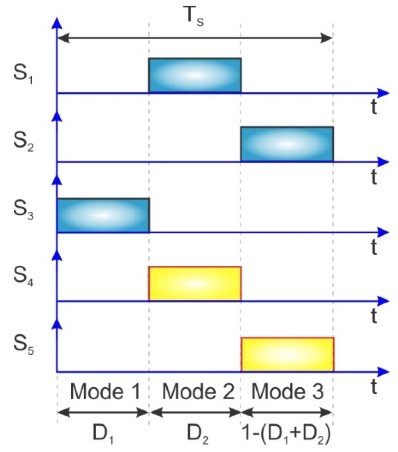
A Timing diagram of various modes are shown in Figure 2, where Ts is represented as the switching period. Referring to the diagram of PSLLC converter circuit, S3 behaves as complementary switch for S1, S2 and S4, S5 act as load switches.
Three modes of operation are considered for the proposed converter. In the first mode, S3 is ON and inductor L magnetizes for the period of 0 ˂ t ˂ D1TS. The time period D1TS ˂ t ˂ D2TS is considered as the second mode, where switch S1 and S4 are ON and and inductor L demagnetizes during this period. In the third mode, switch S2 and S5 are ON for the period of D2TS ˂ t ˂ D3TS, where D3 can be expressed as 1 − (D1 + D2). Inductor L demagnetizes in this period and works in continuous conduction mode.

2.2. State Space Analysis of PSLLC Converter

To obtain a mathematical model of the proposed DIDO system, a state-space representation is utilized. Using Kirchoffs’ voltage law and state-space averaging approach, performance equations that describe the converter are obtained.
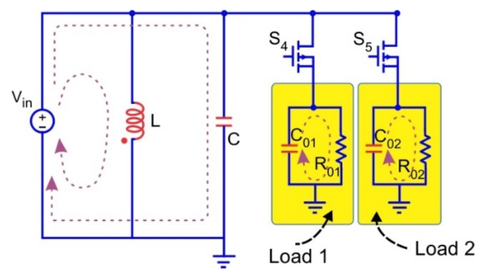
Mode 1: During this mode switch, S3 is ON and S1, S2, S4 and S5 are OFF. From Figure 3 it is understood that the inductor L and capacitor C become parallel connected and are energized respectively for the period of D1Ts. Capacitor C01 and C02 are discharged through the load, assuming capacitor C01 and C02 are charged initially. The state-space equation for inductor current and capacitor voltage are represented in Equation (1).
L di L dt = V in C dV c dt = V in R i L V c R C 01 dV c 01 dt = V c 01 R 01 C 02 dV c 02 dt = V c 02 R 02 }
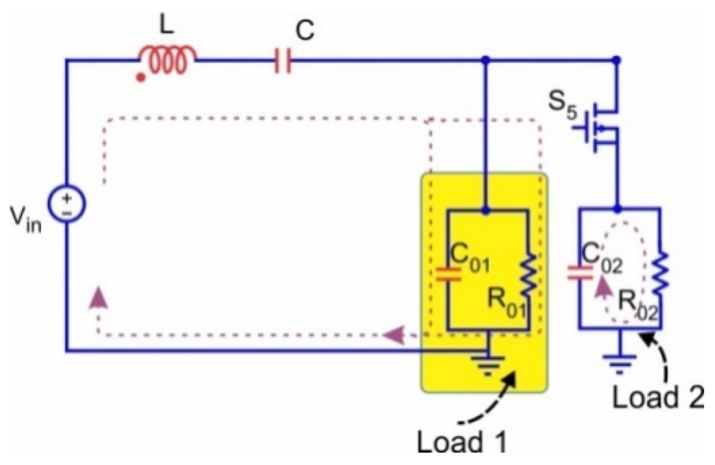
Mode 2: During this mode, the switches S2, S3, S5 are OFF and S1, S4 are ON. Referring to Figure 4, inductor and capacitor de-energize to cater for the load power. Capacitor CO1 charges for the period of D2Ts and CO2 discharges through the load. The state-space equation for the inductor current and capacitor voltage are represented in Equation (2).
L di L dt = V in + V C V C 01 C dV C dt = i L C 01 dV C 01 dt = i L V C 01 R 01 I 1 C 02 dV C 02 dt = V C 02 R 02 }
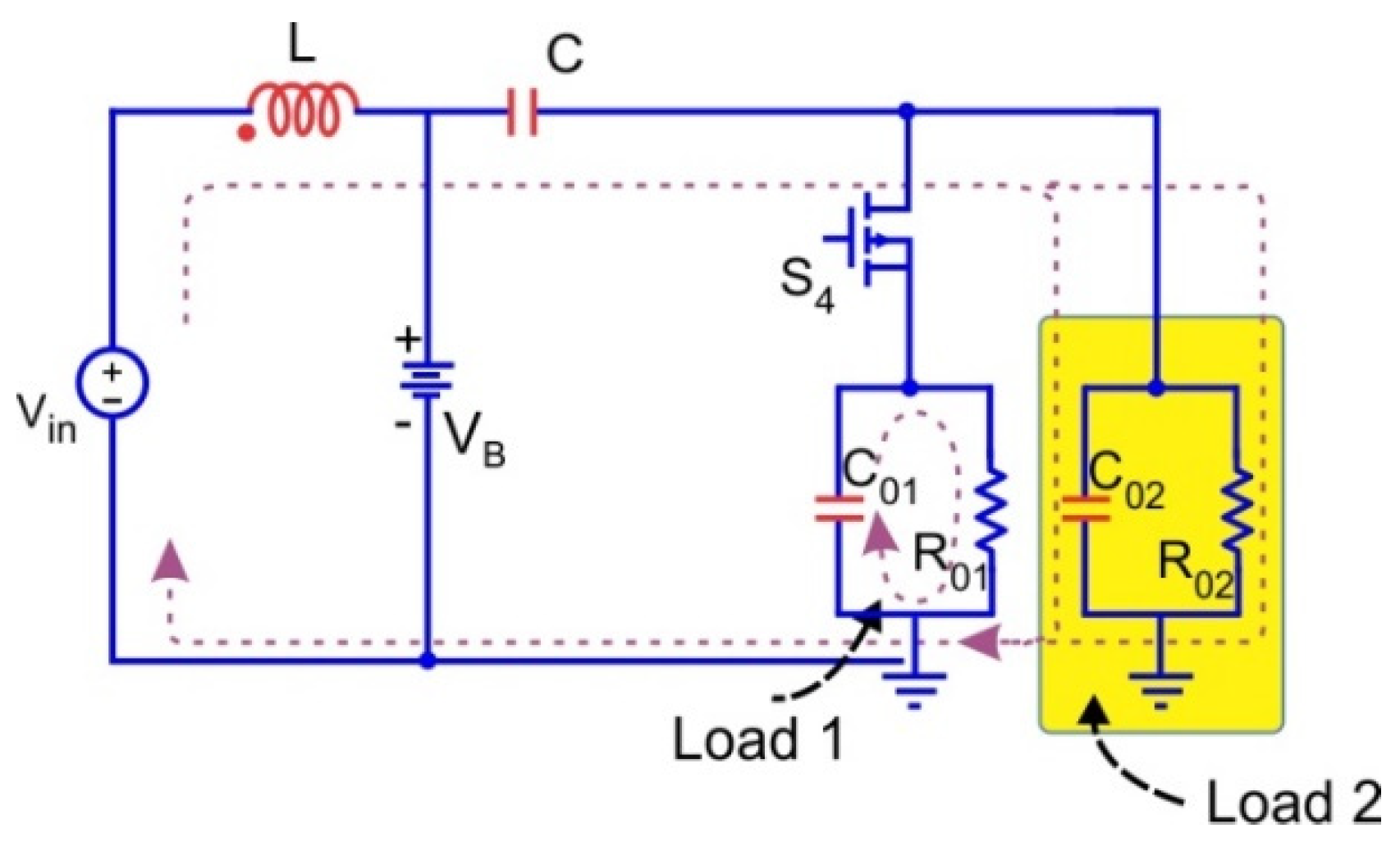
Mode 3: While switching OFF the switch S3, inductor L and capacitor C will be connected in series and therefore de-energized. Referring to Figure 5, as S2 is ON, the battery is charged through inductor. As S5 is ON, capacitor CO2 charges for the period of (1 − (D1 + D2)) Ts. The state-space equation for inductor current and capacitor voltage are represented in Equation (3).
L di L 1 dt = V in V B C dV C dt = i L V B R C 01 dV C 01 dt = V C 01 R 01 C 02 dV C 02 dt = i L + V B R V C 02 R 02 i 2 }
Thus, the three modes of operations can be summarized as mentioned in Table 1.

Representation of State-Space Analysis

Thus, from the modes of Equations (1)–(3), state-space equations are derived by determining the state and output of the system. The system is modeled using capacitor voltage and inductor currents over a switching period Ts. The state model is represented generally by the Equation (4).
X ˙ = A X + B U Y = C X + D U }
Thus, the representation of state variable (X), input variable (U) and output matrix are given in Equation (5).
A = [ 0 D 2 L 1 D 2 L 1 0 1 2 ( D 1 + D 2 ) C D 1 RC 0 0 D 2 C 01 0 1 R 01 C 01 0 ( 1 ( D 1 + D 2 ) ) C 02 0 0 1 R 02 C 02 ]   B = [ 1 L 1 1 L 1 0 0 D 1 RC 1 RC 0 0 0 0 1 C 01 0 0 0 0 1 C 02 ] C = [ 0 0 1 0 0 0 0 1 ]   D = [ 0 0 0 0 ]
The obtained output voltage equations with respect to duty cycle and input voltages are stated in Equations (6) and (7).
V 01 = [ ( 1 + D 2 ) D 2 ] V in [ 1 D 2 + 1 D 1 ] V B
V 02 = [ ( D 1 + D 2 1 ) D 1 ( 1 D 2 + 1 D 1 ) ] V in [ D 1 + D 2 1 D 1 2 + D 1 + D 2 1 D 1 D 2 + 1 ] V B

2.3. Small Signal Modeling of PSLLC Converters

As the practical system is nonlinear, it is necessary to consider the nonlinearities present in the system. Therefore, combining the perturbations which have small variations over a switching period along with the steady state parameters, the state space variables can be rewritten as: d 1 = D 1 + d 1 ^ , d 2 = D 2 + d 2 ^ , v in = V in + v in ^ , v B = V B + v B ^ , i 1 = I 1 + i 1 ^ , i 2 = I 2 + i 2 ^ , v C = V C + v C ^ , v 01 = V 01 + v 01 ^ , v 02 = V 02 + v 02 ^ , i L = I L + i L ^ . Neglecting the higher order components, the steady state equation can be transformed as x . = A x ^ + B u ^ and equating steady state element equal to zero, the matrices thus obtained are represented in Equation (8).
d dt [ i L ^ v C ^ v 01 ^ v 02 ^ ] = [ 0 D 2 L D 2 L 0 ( D 1 + D 2 ) C D 1 RC 0 1 ( D 1 + D 2 ) R 02 C D 2 C 01 0 1 R 01 C 01 0 1 ( D 1 + D 2 ) C 02 0 0 1 R 02 C 02 ] [ i L ^ v C ^ v 01 ^ v 02 ^ ] + [ 1 L 1 L 0 0 0 V C V 01 L D 1 RC 1 RC 0 0 [ 2 I L C + V c RC ] 2 I L C 0 0 1 C 01 0 0 I L C 01 0 1 R C 02 0 1 C 02 I L C 02 I L C 02 ] [ v in ^ v B ^ i 1 ^ i 2 ^ d 1 ^ d 2 ^ ]
With the designed values of inductor L, Capacitors C, C01, C02, the transfer functions of the output voltage with respect to control variables can be derived as shown in the Equations (9)–(12).
G 11 ( s ) = V 01 d ^ 1 = 1.128 × 10 10 s 2.096 × 10 13 s 4 + 2090 s 3 + 3.627 s 2 2.614 × 10 8 s 1.012 × 10 10
G 12 ( s ) = V 01 d ^ 2 = 8.5 × 10 4 s 3 1.59308 s 2 1.394 × 10 10 s 5.208 × 10 13 s 4 + 2090 s 3 + 3.62 × 10 5 s 2 2.614 × 10 8 s 1.012 × 10 10
G 21 ( s ) = V 02 d ^ 1 = 8.5 × 10 4 s 3 1.734 × 10 8 s 2 3.902 × 10 10 s 7.953 × 10 12 s 4 + 2090 s 3 + 3.62 × 10 5 s 2 2.614 × 10 8 s 1.012 × 10 10
G 22 ( s ) = V 02 d ^ 2 = 8.5 × 10 4 s 3 1.959 × 10 8 s 2 7.848 × 10 10 s 1.94 × 10 13 s 4 + 2090 s 3 + 3.62 × 10 5 s 2 2.614 × 10 8 s 1.012 × 10 10
Using an adjunct polynomial scheme, the higher order transfer functions G11(s), G12(s), G21(s), and G22(s) can be reduced to second order transfer functions as shown in Equations (13)–(16).
G 11 ( s ) = V 01 d ^ 1 = 1.128 × 10 10 s 3.848 × 10 6 s 2 722.09 s 27955.8
G 12 ( s ) = V 01 d ^ 2 = s + 3736 s 2 722.09 s 27955.8
G 21 ( s ) = V 02 d ^ 1 = 8.5 × 10 4 s 0.16 × 10 6 s 2 722.09 s 27955.8
G 22 ( s ) = V 02 d ^ 2 = 8.5 × 10 4 s 0.478 × 10 8 s 2 722.09 s 27955.8
The Bode plot is drawn for the transfer functions [13,14,15,16], which shows the existence of cross-regulation in the proposed converter.

2.4. Effect of Cross-Regulation in an Open Loop MIMO Structure of PSLLC Converter

To obtain a stable system, it is necessary to examine the Bode plot for the transfer functions depicted by Equations (13)–(16). The bode plots of transfer functions relating output voltage to duty cycle are obtained and represented in Figure 6 for second order system of G11(s), G12(s), G21(s), and G22(s), where blue graph is the direct transfer function for output voltages and the red graph indicates the cross-coupling transfer function. The Bode plots of coupled transfer function show the phase margin Pm as −90 and indicates that the system is unstable. The existence of coupling between the output voltages makes the closed-loop system destabilized, and tuning becomes difficult. Thus, elimination of interaction using decoupling methodology for voltage control is discussed in Section 3.

3. Close Loop Controller

To suppress the cross-regulation and to regulate the line and load voltages within the operating limit, it is necessary to design a controller. Therefore, in this paper, two different controllers, a conventional PID controller and a DMPC controller, are discussed.

3.1. Conventional Controller

3.1.1. Decoupling Method

As the proposed converter has a strong coupling effect between input and output, there is nonlinearity, which makes tuning difficult for the individual loop. In the decoupling technique, cross-coupled loops are segregated and considered as individual loops (a MIMO system is converted into SISO system) to reduce the complexity in the coupled network. By separating the loops, the PID controller can be independently controlled for better performance. Figure 7 shows the DIDO structure, representing d1 and d2 as input variables and V01 and V02 as the output variables. The input and output variables are related to the transfer function, as shown in Equations (17) and (18). The change in d1 affects V01 and V02. Similarly, the change in d2 affects V02 and V01. This coupling effect makes the system unstable. Therefore, the decoupling method is preferred, to overcome the interaction between the control variables.
V 01 = G 11 ( S ) d ^ 1 + G 12 ( s ) d ^ 2
V 02 = G 21 ( S ) d ^ 1 + G 22 ( s ) d ^ 2
G ( S ) = [ G 11 ( s ) G 12 ( s ) G 21 ( s ) G 22 ( s ) ]
To determine the best pairing for the MIMO system from Equation (19) and to measure process interactions, relative gain array (RGA) and Niederlinski index (NI) tools are employed. RGA requires that negative pairing not be selected, and that the pair which is approximately equal to one be chosen. If the NI ˂ 0 system is integral unstable and if NI = 0, a favorable interaction is possible. The formulae to calculate RGA are mentioned in Equations (20)–(22).
Λ = [ λ 11 λ 12 λ 21 λ 22 ]
λ ij = open   loop   gain closed   loop   gain
NI = | K | Π i K ii
Figure 8 shows the decoupled network of the DIDO system. It indicates that by adding G 21 / G 22 in the network, G 21 term is eliminated, which in turn affects the second output. Similarly, by adding G 12 / G 11 in the network, G 12 term is eliminated, which affects the first output. Thus, multi-loop interactions are nullified and two individual loops are obtained which are independent of each other by transforming the transfer function matrix into a diagonal one as shown in Equation (23).
G = XU 1 G 1 ; U = [ d 1 d 2 ] T
From Figure 8, G′(s) can be calculated using a diagonal matrix, and are expressed as Equations (24)–(26).
G ( s ) = [ 1 G 12 ( s ) G 11 ( s ) G 21 ( s ) G 22 ( s ) 1 ]
G 1 ( s ) = V 01 d ^ 1 = G 11 ( s ) G 21 ( s ) G 22 ( s ) G 12 ( s )
G 2 ( s ) = V 02 d ^ 2 = G 22 ( s ) G 12 ( s ) G 11 ( s ) G 21 ( s )
By using adjunct polynomial scheme for reduction of higher order system to second order system, the second order transfer function is expressed as shown in Equations (27) and (28).
G 1 ( s ) = V 01 d ^ 1 = 5.179 × 10 6 s + 1.0297 × 10 3 s 2 + 10.558 s 22.695
G 2 ( s ) = V 02 d ^ 2 = 6.466 × 10 3 s 0.4258 s 2 + 11.714 s + 6.4287 e 5
Thus, the DIDO controller is converted to two individual PID controllers with SISO model.

3.1.2. Design of PID Controller

To obtain the desired regulated voltage, and to enhance the performance, the PID controller is tuned using the Ziegler and Nichols method. By tuning, the gain of proportional and integral value of the conventional controller is designed to vindicate the cross-regulation effect based on the requirements of load disturbance. Controller output C(s), with respect to the error E(s), is expressed in transfer function in the Equation (29).
C ( s ) E ( s ) = K p ( 1 + K i s + K d s )
For the individual loop of G 1 ( s ) and G 2 ( s ) , the controller transfer function is obtained as stated in Equations (30) and (31).
C 1 ( s ) E 1 ( s ) = 2.801 ( 1 + 1.748 e 15 s + 0 s )
C 2 ( s ) E 2 ( s ) = 3.052 ( 1 + 2.099 e 15 s + 0 s )
The PID controller reduces the cross-regulation. However, it has a variety of drawbacks. For the DIDO system, the system has to be divided into two SISO systems and thus two PID Loop are applied, which increase the complexity of the system. The future trajectory of outputs cannot be determined, as PID emphasizes its effect on error signal rather than on the controlling variables. Moreover, PID takes time to reach a stable operation and suffers from overshoot conditions without proper damping, which affects the steady state error. The PID controller needs to be tuned for every different case or change in system dynamics. This is not ideal to regulate cross-regulation. To overcome all these drawbacks, DMPC is designed.

3.2. Digital Model Predictive Controller (DMPC)

Digital model predictive controller (DMPC) depends on dynamic models that can be developed by system identification. The cost function defines the system behavior of the variables, such as inductor current and the capacitor voltage, that can be used to anticipate the function of desired output voltage. The instantaneous values IL, VC are represented by I(k)L and V(k)C. These values are fed from the system and are used to find out the predicted values of IL, VC, which are represented as I(k + 1)L and V(k + 1)C. As mentioned in the literature, the predictive values can be obtained by a variety of state estimation methods like Kalmann filter, Lagrangian extrapolation, Newton-Raphson method, and Euler’s method. While constructing the predictive model, the controlled variables, that is, VC and IL must be measured with the aim of attaining the discrete-time models. The discrete-time model is used to predict the future value of controlled variables at the kth sampling instant. Several discretization methods are used in order to obtain a discrete-time model appropriate for the predictive calculation. Considering that the load can be modelled as a lower order system, the discrete-time model can be obtained by forward Euler’s method, which has a simple approximation of the derivative. However, for more complex systems, this approximation may introduce errors into the model and a more accurate discretization method is required. The other methods are used for higher order derivatives. By constructing the sequence of successive approximations, estimated values are obtained accurately. According to the forward Euler approach, the future values of controlled variables are estimated by considering the current values of the system inputs as shown in Equation (32):
( k + 1 ) = x ( k ) + T s ( f ( x ( k ) , u ( k ) )
where Ts is sampling time and f(x(k), u(k)) is change in state variables obtained from state-space analysis. Applying this formula, the values of I(k + 1)L and V(k + 1)C are obtained. Using the predicted values of control variables, cost function is represented as shown in Equation (33):
J = | | ( k + 1 ) x ( k + 1 ) | | 2
where (k + 1) is the reference value and x (k + 1) is the anticipated value of the controlled variable considered from the discretized system model. If the system has more than one main control variable, then the cost function can include control parameters X1 and X2 with the help of weighting factor λ as shown in Equation (34):
J = | | X 1 ( k + 1 ) ref X 1 ( k + 1 ) p + λ ( X 2 ( k + 1 ) ref X 2 ( k + 1 ) p ) | | 2
Thus, for the proposed converter, the controlling parameters are IL and VC, therefore, the cost function is replaced as mentioned in Equation (35).
J = | | I L ( k + 1 ) ref I L ( k + 1 ) p + λ ( V C ( k + 1 ) ref V c ( k + 1 ) p ) | | 2
The cost function J is reduced for the entire control horizon i.e., the duration at which the plant is to be controlled. This produces the optimal condition at which the output of the system is required. For switching combinations, the proposed converter has two switches (MOSFETs) which control the load voltage; as a result the following set S is derived with respect to various possible switching combinations: S = { ( 0 , 0 )   ( 0 , 1 )   ( 1 , 0 )   ( 1 , 1 ) } .
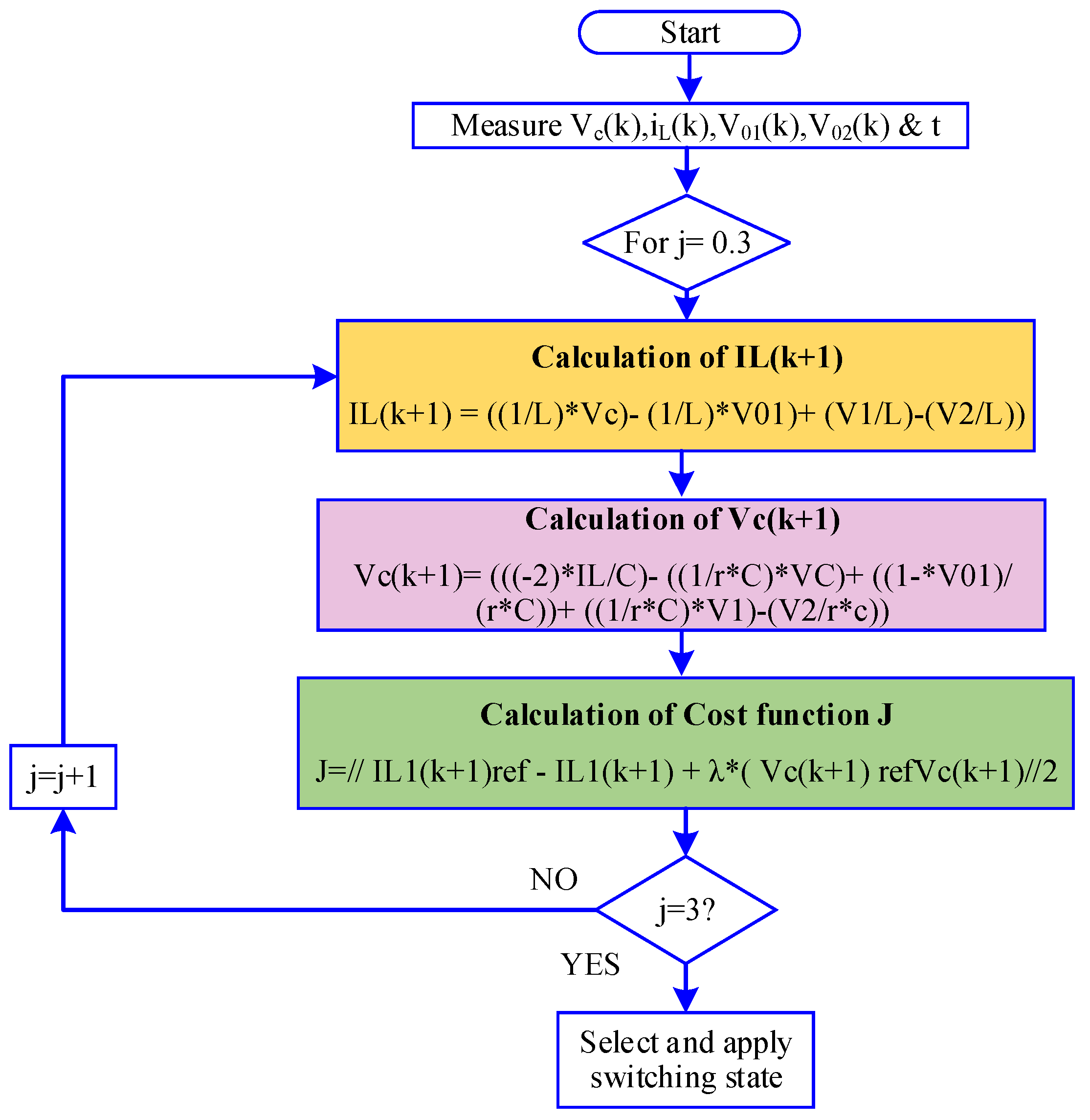
The value of S (1) to S(n) is allocated on the basis of our optimization of cost function, so when the value of J is min, use S (1) combination and then gradually increase to S(n) for the max value of J. This entire process is repeated for the complete duration of prediction horizon and control horizon. This thus allows proper switching of the converter, which helps in regulating the output voltages. Therefore, for any variation in load, the DMPC ensures a steady switching operation such that the load variations are handled with ease, thus minimizing cross-regulation. This algorithm is implemented in MATLAB Simulink. The DMPC controller is employed by replacing the PID controller. The inputs of DMPC controller are IL (inductor current), V01 (output voltage across load1), V02 (output voltage across load2), Vin1 (PV Input voltage), Vin2 (battery Input voltage), VC (capacitor voltage), and t (simulation time). The outputs of the DMPC controller are the switching pulses for two switches across the load output. Figure 9 shows the flowchart of the DMPC algorithm.
A control scheme for DMPC applied to the power electronic interface circuit (PSLLC) converter is shown in Figure 10. In this scheme, the output voltage and the current are used as measured variable which is used in the model to estimate the predicted output for n possible actuations. These predicted values and the reference values are evaluated and the error is minimized by the cost function J. The optimal switching state S is selected, which is applied to load switch in the PSLLC converter. Thus, for any variation in one load, the proposed controller allows the proper switching state to the converter, thereby reducing the cross-regulation. Thus, the following points are summarized for the DMPC controller:
  • The instantaneous value of inductor current and capacitor voltage are considered as the reference values which are represented as I*(k)L and V*(k)C.
  • From the load side, the instantaneous values of inductor current and the capacitor voltage are measured and signified as I(k)L and V(k)C.
  • These values are fed to the predictive model to find the predicted values of I(k + 1)L and V(k + 1)C.
  • The error obtained by the reference value and the predicted values are measured and minimized by the cost function J for the entire control horizon.
  • The optimal actuation is attained by minimizing the cost function J, and the corresponding switching state is produced, which controls the load switch effectively, thus minimizing the cross-regulation.

4. Design Procedure

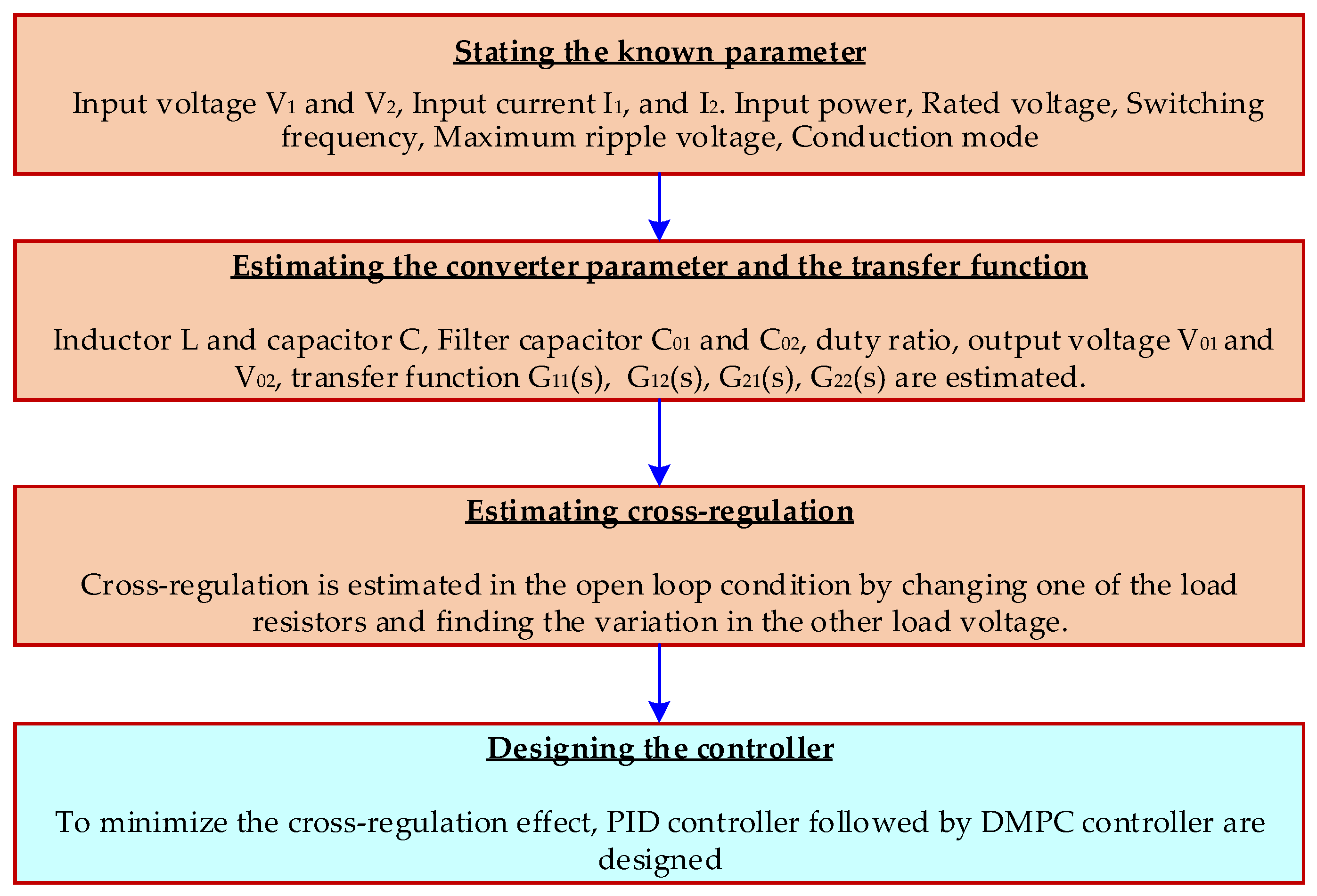
The components used in the proposed converter are designed for the maximum power range of 250 W. The input sources are considered as fixed DC input and battery input. The following points are considered for the converter design as shown in Figure 11.
To determine the parameters of the components used in proposed converter, the following specifications are considered.
(a)
The input voltage V1 and V2—40 V, 20V
(b)
The input current Iin —4 A
(c)
Ripple voltage—±0.1%
(d)
Ripple current—±5%
(e)
Switching frequency—100 KHz
(f)
Conduction mode—continuous
(g)
Duty cycle are taken in the range of (0.2–0.7)
(h)
The output voltage of the converter is in the range of (60–65) V
(i)
The output current is in the range of (2–3) A
(j)
The minimum value of the inductor is calculated using the formula: L V in D 1 F s Δ i _ L = 1 mH
(k)
The minimum value of the capacitance is calculated using the formula: C V 01 R D 1 F s Δ V 01 where C = C01 = C02 = 680 µF
(l)
The presence of cross-regulation in the system in MATLAB Simulink in open loop condition is verified and estimated. By means of a circuit breaker, a step change across the load R01 is introduced during the simulation runtime, using parallel resistance connection. This load variation causes a subsequent variation in the voltage and current across R02 which is calculated as follows:
Cross-regulation (%) = (V02peak − Vo2drop) × 100/V02peak = (93.5 − 90) × 100/93.5% = 3.74%
Based on this design of the converter, the proposed controller is simulated and tested for different load conditions.

5. Performance Analysis Based on Simulation and Experimental Results

The proposed converter shown in Figure 1b is simulated in MATLAB-Simulink platform. The DIDO PSLLC converter is designed to a set of specifications mentioned in Table 2. Based on the availability of industrial products, the input source and the load specifications are considered. The inductor and capacitor values are selected based on the voltage ripple calculations. Different case studies for line regulation and load regulation are carried out.

5.1. Simulation of PID Controller

For steady state operation, the proposed converter has V01 = 103V, V02 = 94 V, and current I01 = 4.08 A, I02 = 4.63 A at R1 = 25 Ω, and R2 = 20 Ω. Different cases are discussed for the evaluation of cross-regulation in the proposed converter using the PID controller. To analyze the cross-regulation effect, a breaker is introduced for the load change in one output and the corresponding changes are observed in the other output.
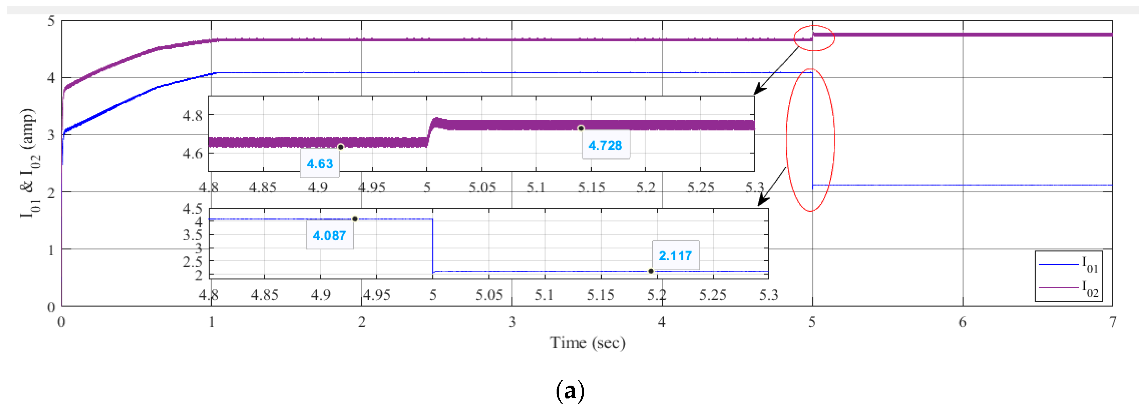
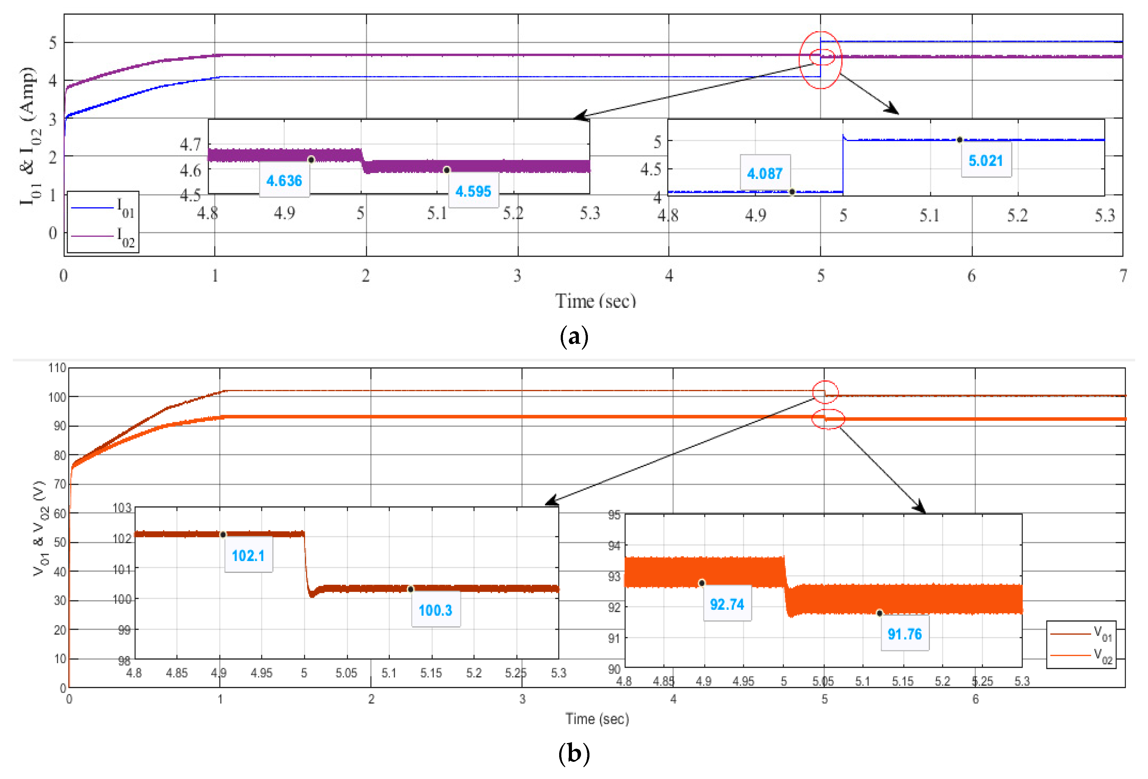
Case 1: Higher step change at load output 1: Under steady state operation, load current Io1, Io2 are found to be 4.087 A, 4.63 A respectively. At t = 5 s, the load resistance R1 is stepped up from 25 Ω to 50 Ω and the results are displayed in Figure 12. It can be seen that the output current I01 decreases from 4.08 A to 2.117 A as the load increases. Due to decremented change in I01 current, the other load current I02 increases from 4.63 A to 4.728 A, and the output voltage V01 and V02 are modulated with respect to change in load. The load decrement in I01 does not affect the second load current I02, and it is regulated with the difference of 0.098 A, while the cross-regulation is calculated as 0.02 (or 2%). Thus the controller effectively suppresses the cross-regulation for the higher load change but the step change in the first load modulates the output voltage and produces a ripple in V02.
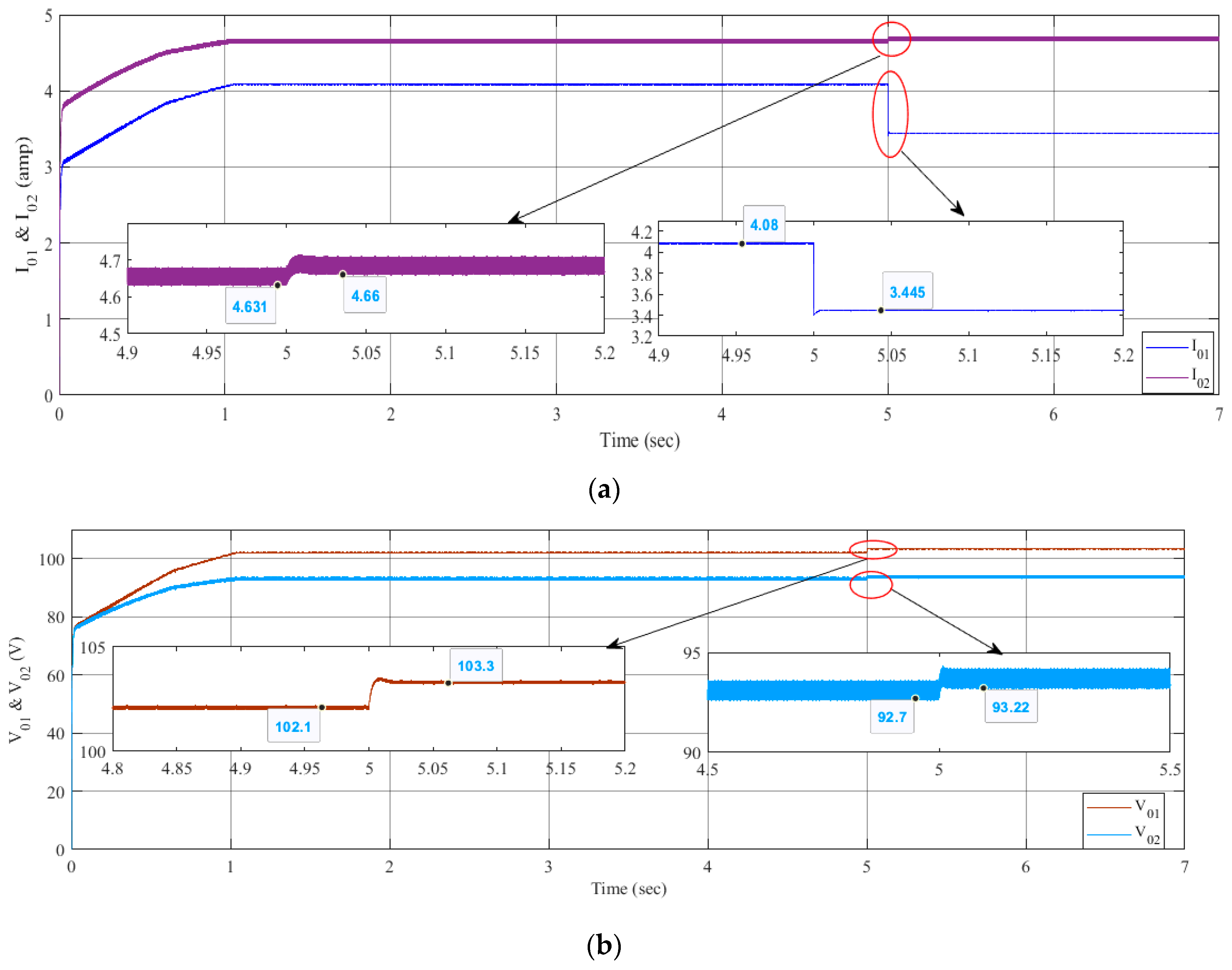
Case 2: Moderate step increase at load output 1: At t = 5 s, the load resistance R1 is stepped up from 25 Ω to 30 Ω and the results are displayed in Figure 13. It is clearly seen that the output current I01 decreases from 4.08 A to 3.445 A as the load increases. Due to decremented change in I01 current, the other load current I02 increases from 4.63 A to 4.66 A, and the output voltage V01 and V02 are modulated with respect to change in load. The full load decrement in I01 does not affect the second load current I02, and it is regulated with the difference of 0.03 A, while the cross-regulation is calculated as 0.008 (or 0.8%). Thus, the proposed controller is able to suppress the cross-regulation for the moderate load change but it produces ripples in the output voltage V02.
Case 3: Moderate step decrease at load output 1: At t = 5 s, the load resistance R1 is stepped down from 25 Ω to 20 Ω and the results are displayed in Figure 14. It can be seen that the output current I01 increases from 4.08 A to 5.021 A as the load decreases. Due to the incremental change in I01 current, the other load current I02 decreases from 4.63 A to 4.595 A, and the output voltage V01 and V02 are modulated with respect to change in load. The slight increment in I01 does not affect the second load current I02, and it is regulated with the difference of 0.041 A, while the cross-regulation is calculated as 0.006 (or 0.6%). Thus, the controller reduces the cross-regulation for the moderate load change but sudden change produces ripples in the output voltage V02.
From these results, it is understood that the cross-regulation was reduced to an acceptable level of 0.6 to 2% for various cases of step change in the load. The drawback is the requirement of two PID controllers, to control the switches across the two loads, which produces rippled output. This may increase the complexity of the converter. To overcome this difficulty and to obtain a faster response, a DMPC controller is utilized.

5.2. Simulation of DMPC Controller

The PSLLC was simulated in MATLAB for closed-loop condition with a digital model predictive controller (DMPC). To analyze the DMPC controller and to compare its performance with the PID controller, the same cases are discussed for the evaluation of cross-regulation.
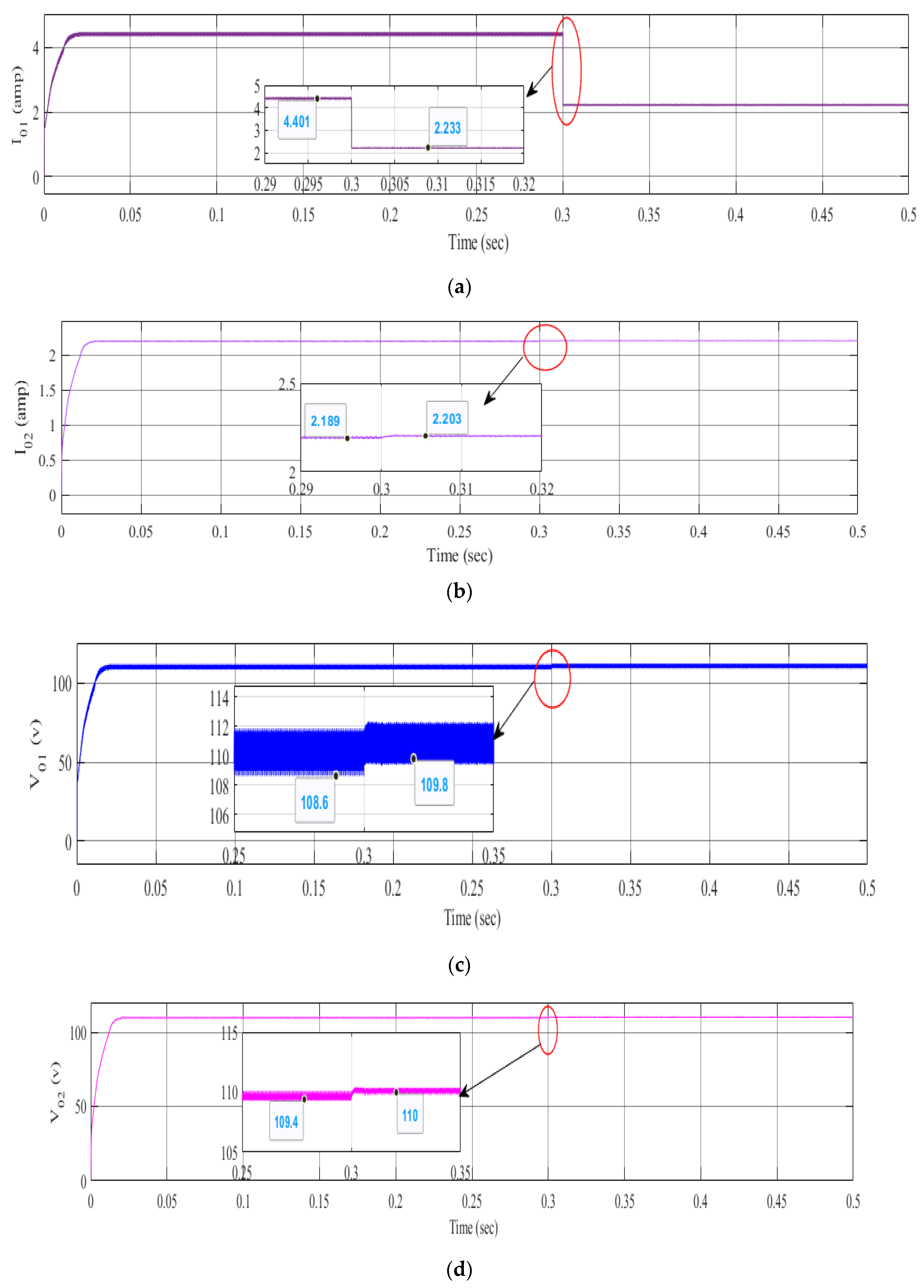
Case 1: Higher step change at load output 1: At t = 0.3 s, the load resistance R1 is stepped up from 25 Ω to 50 Ω and the results are displayed in Figure 15. It can be seen that the output current I01 decreases from 4.401 A to 2.233 A as the load increases. Due to decremental change in I01 current, the other load current I02 increases from 2.189 A to 2.203 A, and the output voltage V01 and V02 are controlled to track the reference voltage just before and after the higher load change at any of the output. The load change in I01 does not affect the second load current I02 and it is regulated with the difference of 0.014 A and the cross-regulation is estimated as 0.006 (or 0.6%). Therefore, the proposed controller effectively suppresses the cross-regulation for the higher load change at any one of the outputs.
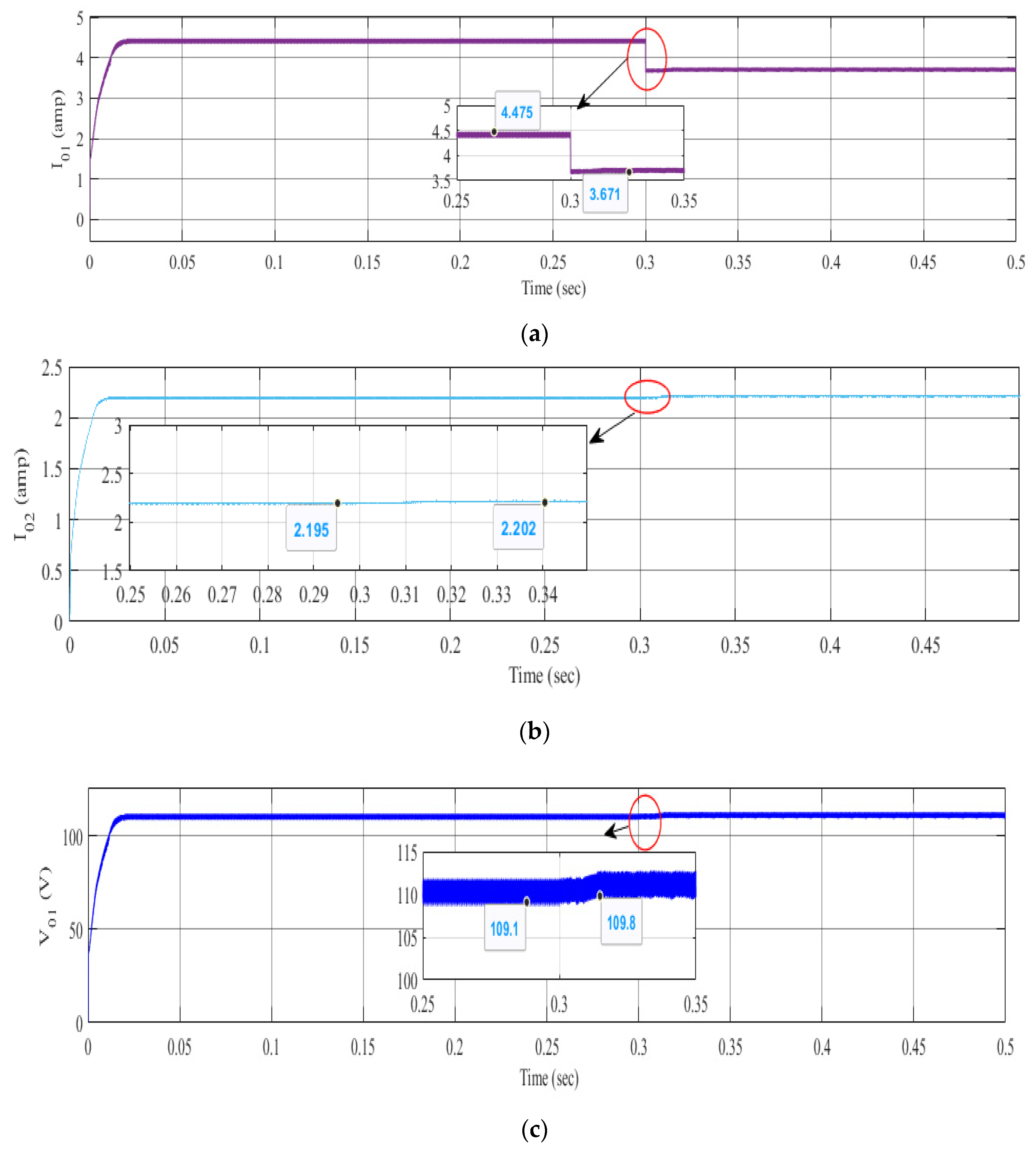
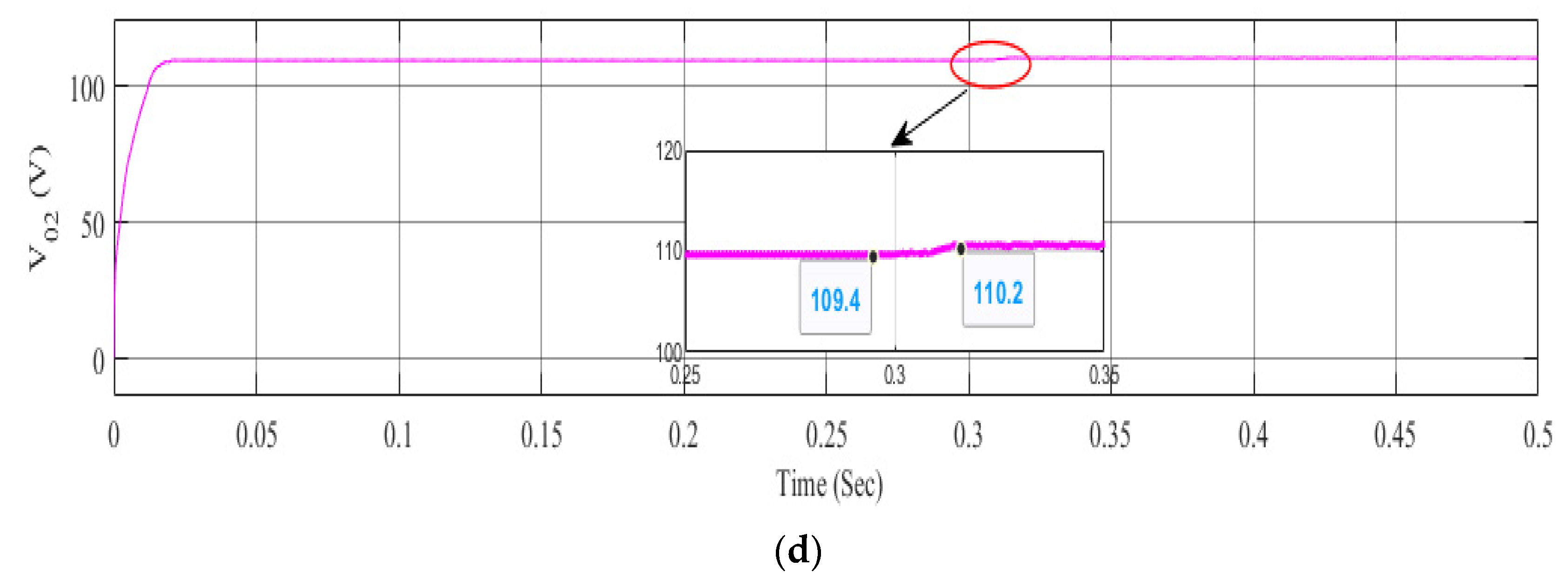
Case 2: Moderate step increase at load output 1: At t = 0.3 s, the load resistance R1 is stepped up from 25 Ω to 30 Ω and the results are displayed in Figure 16. It can be seen that the output current I01 decreases from 4.475 A to 3.671 A as the load increases. Due to decremented change in I01 current, the other load current I02 increases from 2.195 A to 2.202 A and the output voltage V01 and V02 are controlled to track the reference voltage nearly before and after the moderate load change at any of the output. The full load change in I01 does not affect the second load current I02, and it is regulated with the difference of 0.007 A, while the cross-regulation is calculated as 0.004 (or 0.4%). Thus, the controller effectively minimizes the cross-regulation for the moderate load change at any one of the outputs.
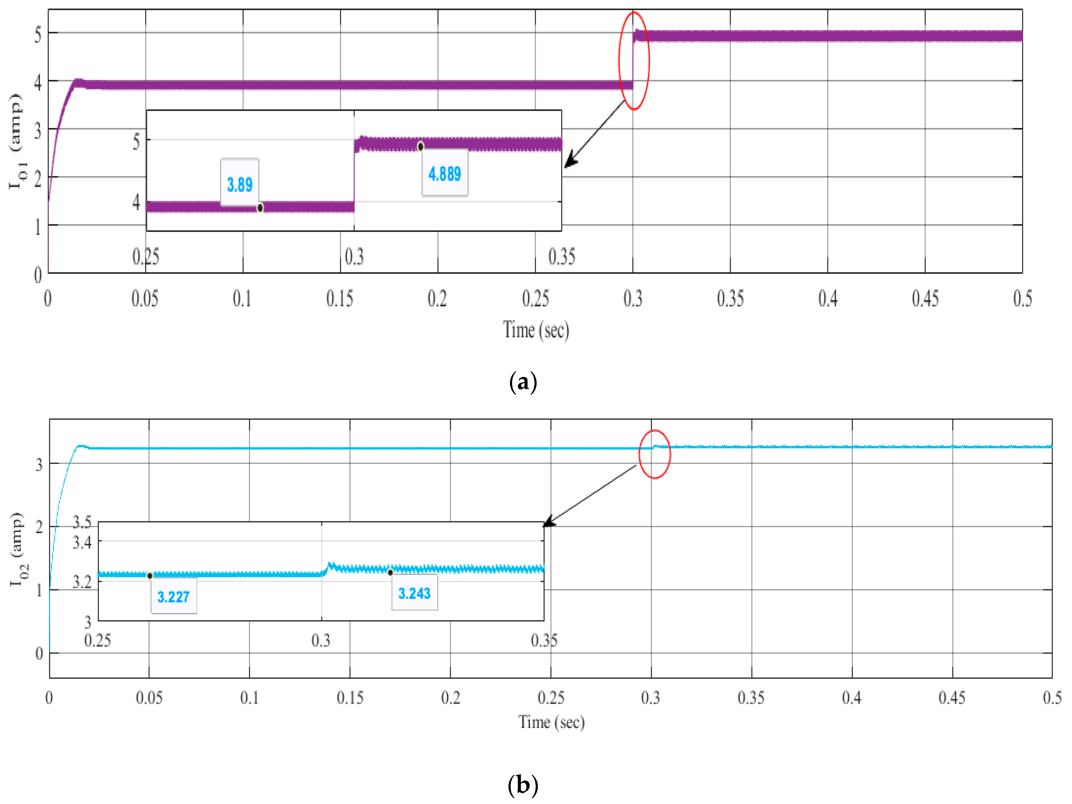
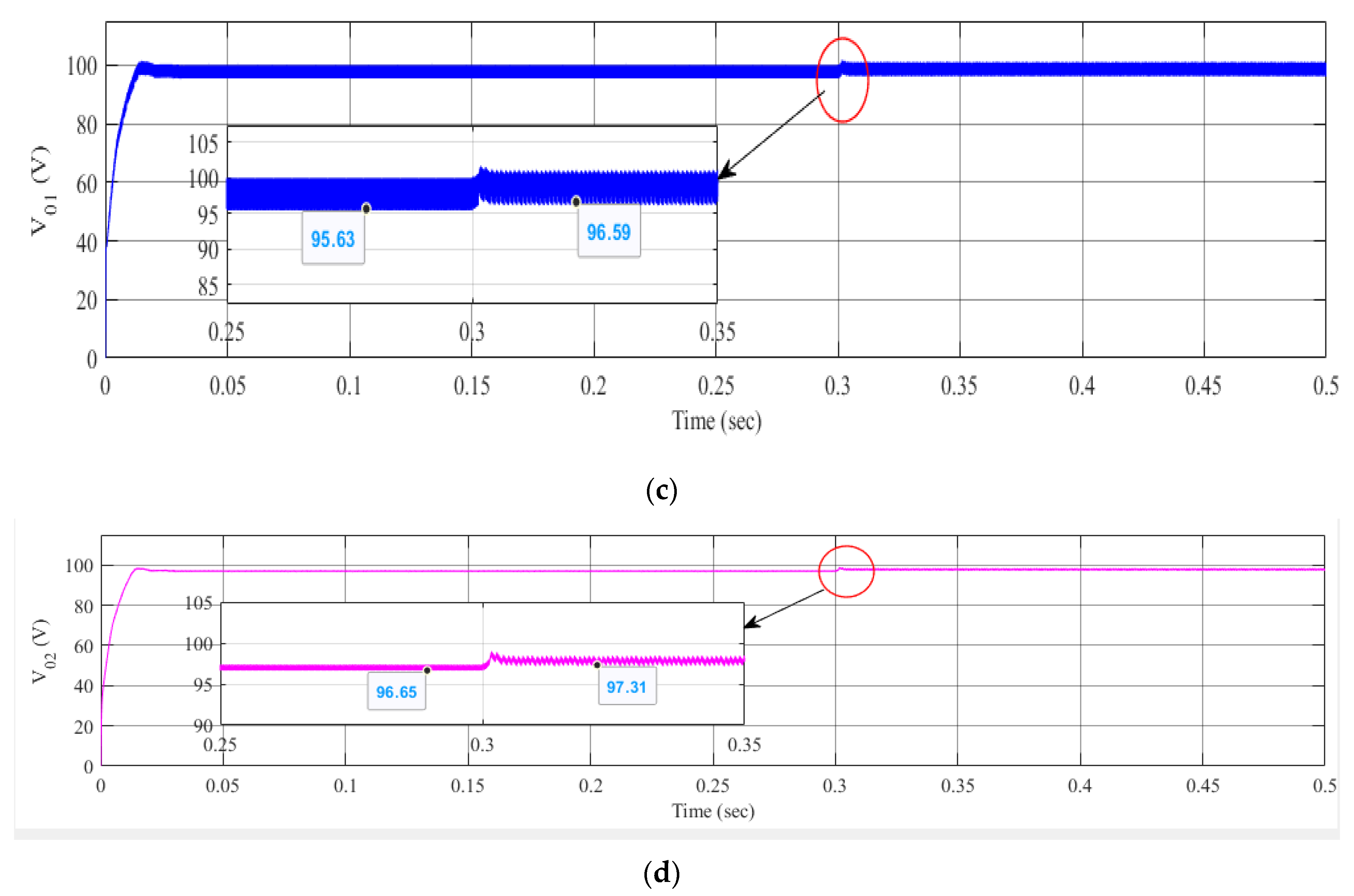
Case 3: Moderate step decrease at load output 1: At t = 0.3 s, the load resistance R1 is stepped down from 25 Ω to 20 Ω and the results are displayed in Figure 17. It can be seen that the output current I01 increases from 3.89 A to 4.889 A as the load decreases. Due to incremental change in I01 current, the other load current I02 changes from 3.227 A to 3.243 A, and the output voltage V01 and V02 are controlled with respect to change in load. The slight increment in I01 does not affect the second load current I02, and it is regulated with the difference of 0.016 A, while the cross-regulation is calculated as 0.003 (or 0.3%). Thus, the controller effectively overcomes the cross-regulation effect for the step decrease in load change either at R01 or R02.
Use of the DMPC shows that the cross-regulation is reduced from 0.3% to 0.6%. The designed DMPC, when compared to a conventional PID controller shows greater performance.

5.3. Comparisons of Various Cases with PID Controller and DMPC Controller

The comparison table shows the various scenarios for analyzing the cross-regulation effect with PID and DMPC controllers. From Table 3, it is observed that the cross-regulation is more reduced in the DIDO system with a DMPC controller than with a PID controller, and the output voltages V01 and V02 are able to track the desired voltage for any change during load regulation. Additionally, it is proved that for any change in load current I01 ranging from 0.1 A to 2 A, the other load current I02 is maintained almost constant with the boundary range between 0.007 A to 0.016 A, thus reducing the cross-regulation to an acceptable value. Without any control loop to the converter and by controlling only the load switches, DMPC minimizes cross-regulation in a much more efficient and effective way than a PID controller. Similar conditions were also tested and validated with a second load. However, those results are not included in this paper.

5.4. Comparison with Existing Works

To illustrate the performance of the developed prototype and its controller, comparisons are made with the existing work in the literature [13,14,15,22,28]. The designed values with the cross-regulation are listed in Table 4. It may be clearly seen that the performance of the designed controller is excellent, by comparing with the key factors such as cross-regulation and the sensitivity index. Cross-regulation is quantified in terms of performance index in [14,15]. The lower the value of cross- regulation, the greater the stability achieved in the converter. Thus, the obtained cross-regulation, in terms of performance index, indicates that the proposed system maintains desirable transient response with the load regulation. Furthermore, in order to highlight the performance of the designed controller, sensitivity indices are estimated. It is proved that the designed controller has a good response by incorporating the step change in load current in one output to other output current variation. The sensitivity (S) index is defined as in Equation (36):
S I out i I out j = ( Δ I out j Δ I out i ) × I out i I out j
where ΔIoutj is change in the output current with cross-channel and ΔIouti is the change in the output current with self-channel. The proposed method has minimum sensitivity indices of 0.012, whereas in [28], it is found to be 0.016, which is calculated based on the step change in voltage variations. It is observed that while calculating the sensitivity index, the value obtained is less than the value mentioned in [13,14,15,22]. In summary, the DMPC controller used in PSLLC converter is superior to the existing methods.

5.5. Experimental Results and Discussion

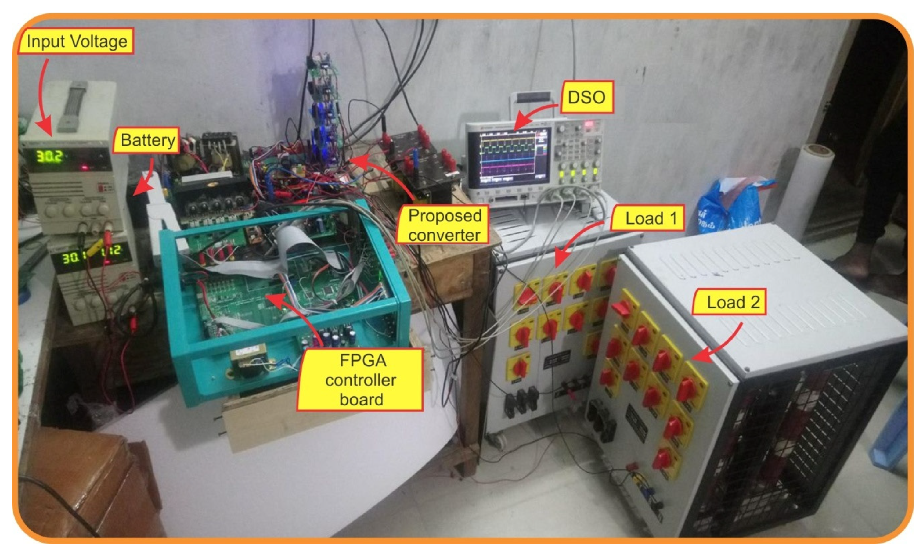
To validate the designed DMPC in an environment where hybrid energy resources are integrated to the loads using PSLLC converter experimentally, a scaled down prototype of 100W capacity is developed, while maintaining the concept of analyzing the cross-regulation effect across the two loads. The dynamic condition is tested and the proposed control strategy is estimated based on Figure 1b with the parameters mentioned in Table 2. Figure 18 shows the hardware model. The prototype model is executed with the aid of FPGA Spartan 6-XC6SLX9 controller board. The components used in the prototype consist of IGBT switch-MG1215H-XBN2MM, PWM driver circuit-ICTLP250, Inductor -IHA 205, Hall Effect sensor-ACS712 for sensing the current, diode rating-ISL9R3060P2, and a 4-inch cooling fan for heat dissipation. Initially, the proposed converter works in the steady state operation. The input voltage for the prototype model is taken as 30V and the obtained output load voltages V01 and V02 are 50 V with IL as 1.93 A. The output voltages are maintained at their reference values without any external disturbance by the designed controller.
Step change is introduced as an external disturbance in the load side and various cases are analyzed which are discussed as follows:
  • Case 1. Step change at load voltage V01:
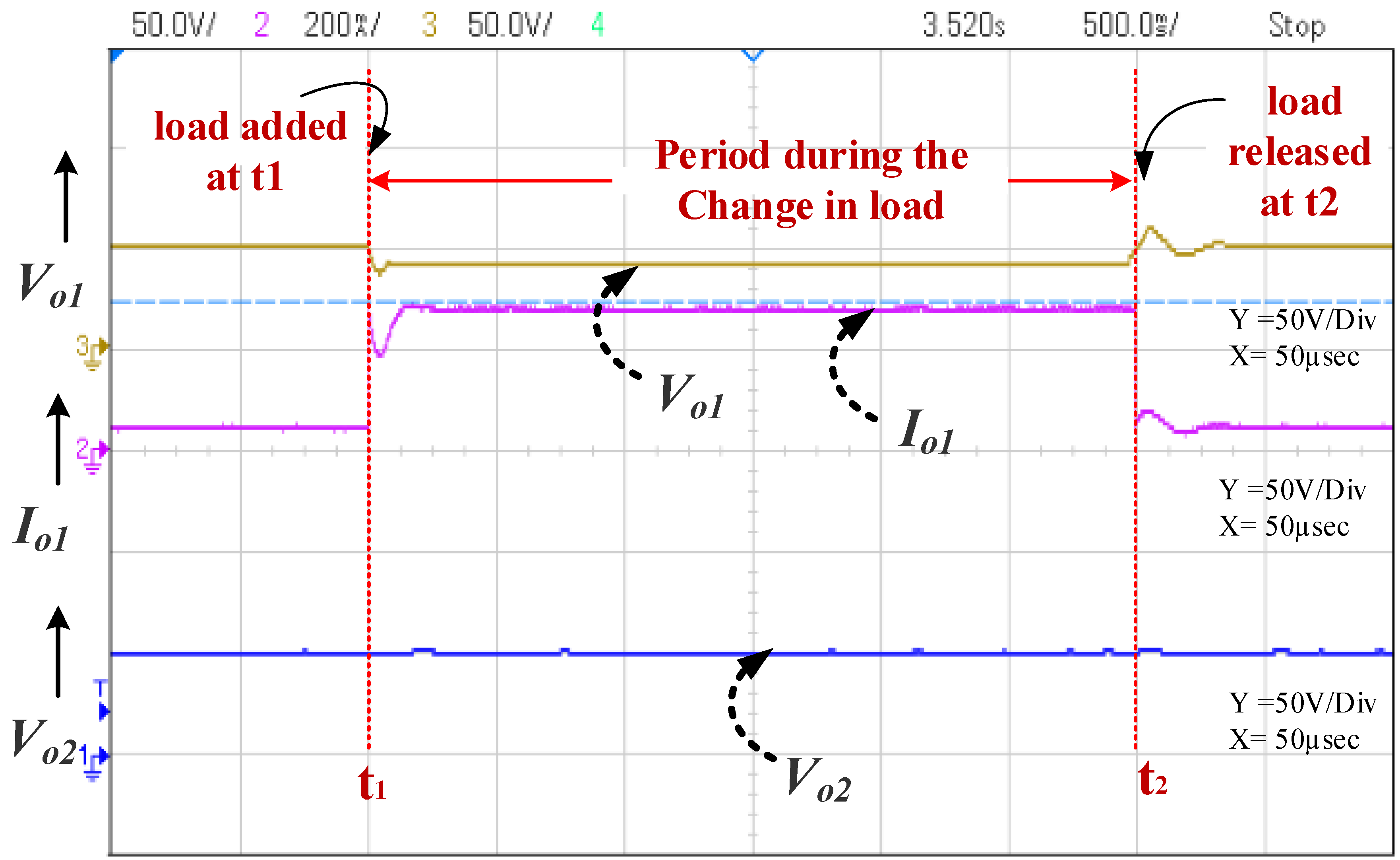
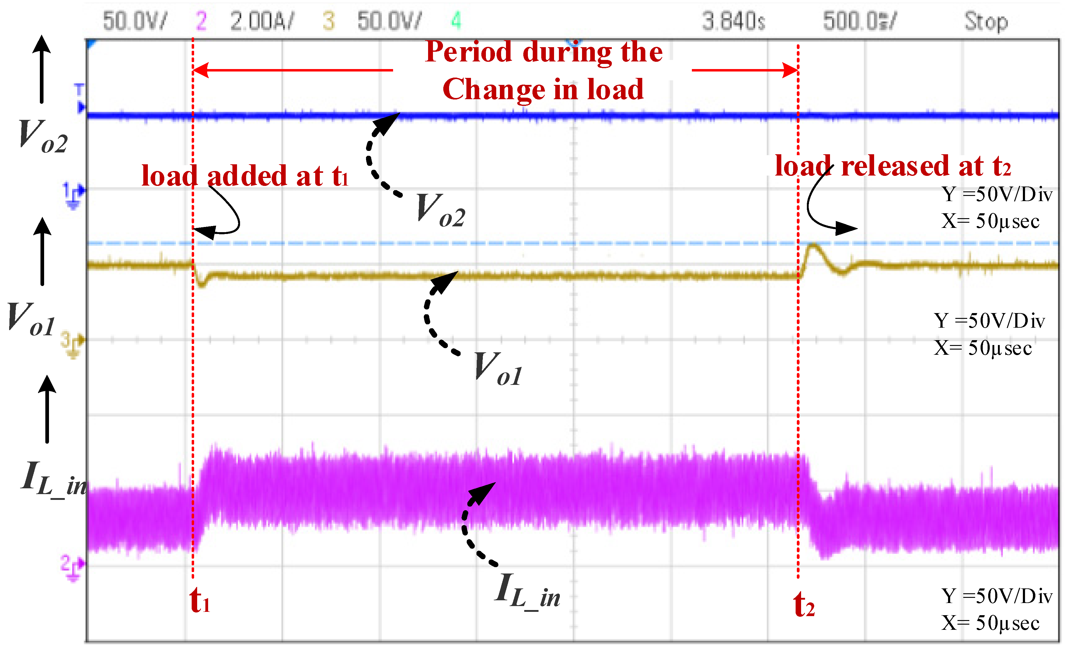
To verify the concept of cross-regulation, a step change is introduced at load 1. Initially, the converter works in steady state mode of operation with I01 = 0.1 mA. At t1 = 1 s, I01 is stepped up from 0.1 mA to 0.4 mA and at t2 = 4 s, I01 is stepped down from 0.4 mA to 0.1 mA. The respective voltage changes in load 1 (V01), drops from 50 V to 49 V at t1 and reverts back at t2. From Figure 19, it is noted that the voltage of second load output V02 is constant, maintaining at 50 V for ensuing step changes in the load current I01. The obtained results of Figure 19 and Figure 20 show that the DMPC controller is capable of reducing the cross-regulation effect with the change in dynamic response.
  • Case 2. Step change at load voltage V02:
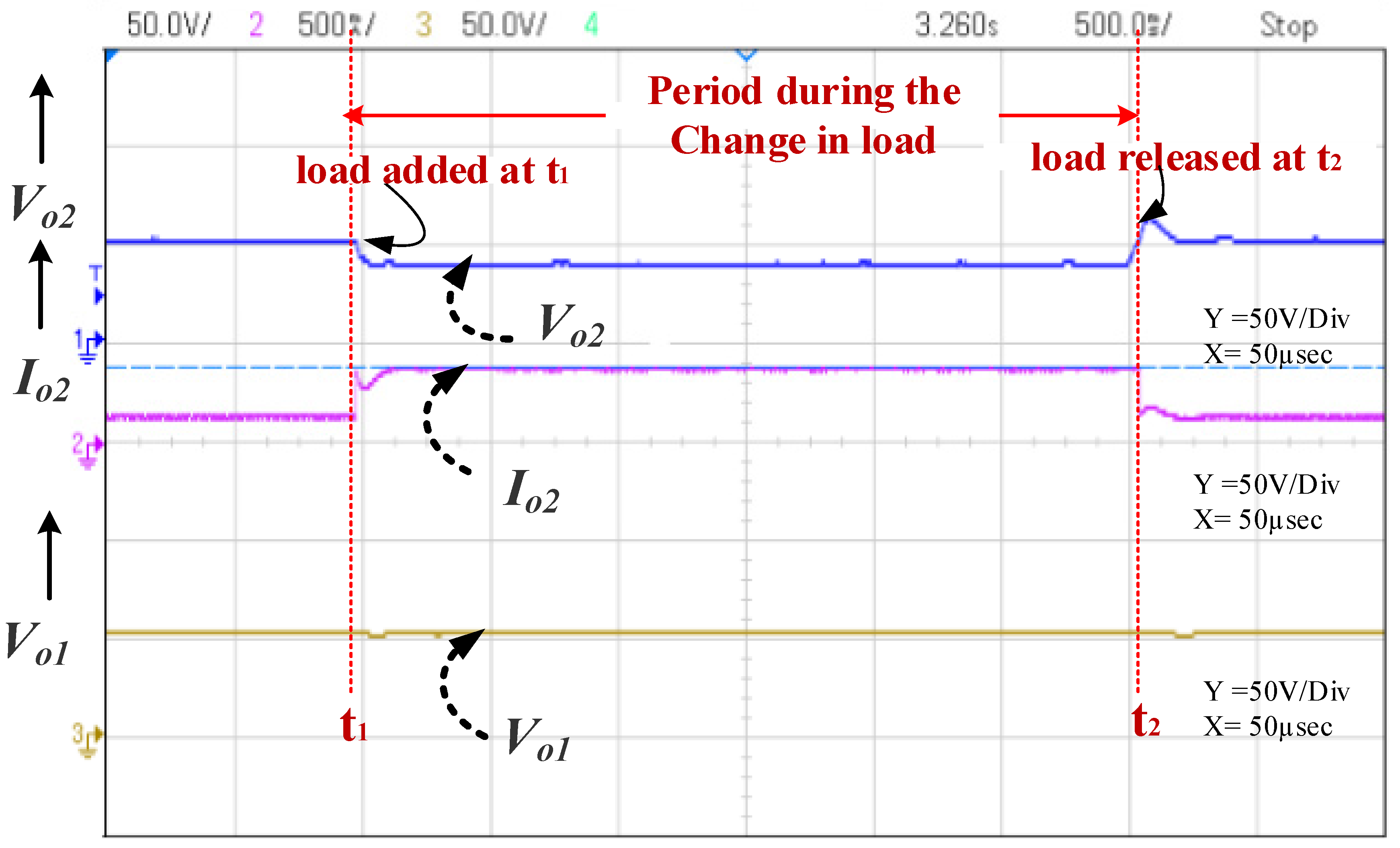
To establish the effect of cross-regulation, a step change is introduced at load 2. Initially, the proposed converter works in steady state mode of operation with I02 = 0.1 mA. At t1 = 1 s, I02 is stepped up from 0.1 mA to 0.4 mA and at t2 = 0.4 s, I02 is stepped down from 0.4 mA to 0.1 mA. The voltage changes in load 2 (V02), drops from 50 V to 49 V at t1, and returns at t2. From Figure 21, it is noted that the voltage of first load output V01 is constant, maintaining a value of 49.8 V for an ensuing step change in the load current I02. The obtained results of Figure 21 and Figure 22 shows that the proposed converter ensures that the output voltages are maintained at their reference values with negligible cross-regulation.
  • Case 3. Step change in input voltage variations:
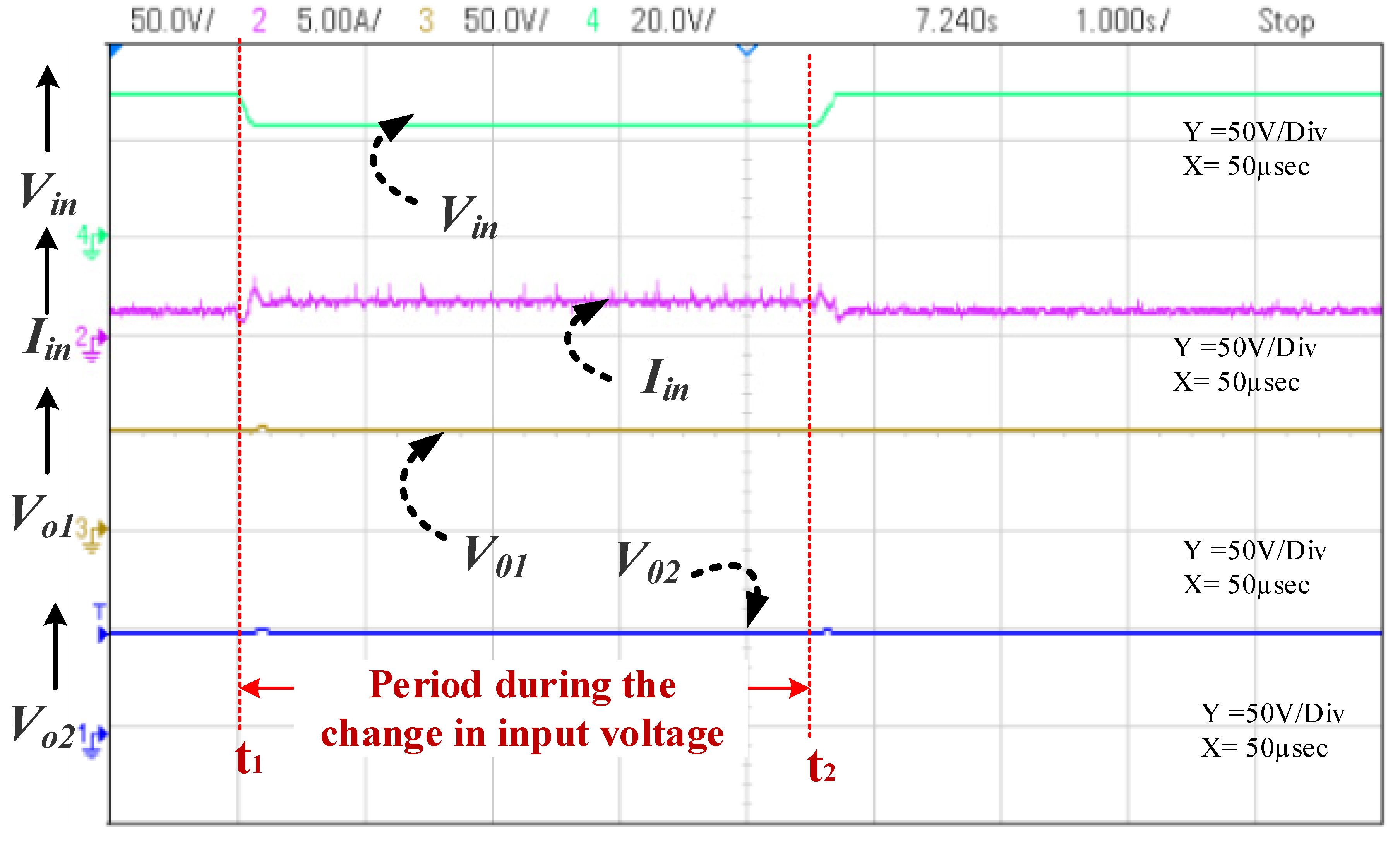
To authenticate the process of line regulation, a step change is introduced in the input voltage while the converter is maintained under steady state operation with I01, I02 = 0.1 mA and Vdc = 30 V. Figure 23 shows the experimental response to the change in the input voltage. During the time period at t1 = 1 s, Input voltage Vin is stepped down from 30 V to 25 V and at t2 = 5.8 s, Vin is stepped up from 25 V to 30 V. Despite the change in the input voltage, load voltage across V01 and V02 remains stable at the desired voltage of 50 V. This case proves the proposed DIDO converter remains stable with respect to change in input voltage. Thus, the results indicate that the designed controller is resistant to any change in input voltage.
The comparison Table 5 shows the various cases obtained by the experimental results. It is proved that for a step change in one load does not affect the other loads, which in turn reduces the cross-regulation effectively.
To summarize the results obtained from Figure 18, Figure 19, Figure 20, Figure 21 and Figure 22, it is clearly shown that the proposed controller has accomplished the job of suppressing the cross-regulation and maintaining the line regulation for various cases of incremental and decremented step change in the resistive loads. The sensitivity index and cross-regulation are estimated in the hardware result and observed to be satisfied with the theoretical values.

6. Conclusions

This paper proposed a digital model predictive controller (DMPC) for DIDO-PSLLC converter to subdue the effect of cross-regulation. At first, the conventional PID controller was designed for the proposed converter and compared with the proposed digital model predictive controller.
This paper proposed a MIMO controller for DIDO hybrid energy system to subdue the effect of cross-regulation. The conclusions are summarized as follows:
  • This paper proposes the PV and battery-connected MIMO positive Super-Lift Luo Converter with high-voltage transfer gain, high power density, high efficiency, reduced ripple voltage and current.
  • The proposed DMPC controller has the advantage of fast dynamic response and suppression of cross-regulation by controlling the load switches. The decoupling method is preferred to overcome the interaction of the proposed hybrid DIDO system with renewable energy resources.
  • The DMPC controller shows greater performance in cross-regulation and sensitivity index when compared with existing literature.
  • Thus, MIMO controller is implemented in a DIDO hybrid energy system, which can be interfaced for electric vehicle application.
Theoretical analysis followed by comparison results proves the outstanding performance of DMPC method in minimizing the cross-regulation in proposed DIDO system. By considering the architecture of the proposed structure, this work can be flexibly extended to an arbitrary number of inputs and outputs. In addition, the proposed converter with the cross-regulation examination can find a place in electric vehicle lighting applications.

Author Contributions

All authors were involved in developing the concept, simulation, and experimental validation and making the article error free and getting a technical outcome for the set investigation work. All authors have read and agreed to the published version of the manuscript.

Funding

This research received no external funding.

Conflicts of Interest

The authors declare no conflict of interest.

References

  1. Rehmani, M.H.; Reisslein, M.; Rachedi, A.; Erol-Kantarci, M.G.; Radenkovic, M.G. Integrating Renewable Energy Resources into the Smart Grid: Recent Developments in Information and Communication Technologies. IEEE Trans. Ind. Inform. 2018, 14, 2814–2825. [Google Scholar] [CrossRef]
  2. Suresh, K.; Chellammal, N.; Bharatiraja, C.; Sanjeevikumar, P.; Blaabjerg, F.; Nielsen, J.B.H. Cost-efficient nonisolated three-port DC-DC converter for EV/HEV applications with energy storage. Int. Trans. Electr. Energy Syst. 2019, 29, 1. [Google Scholar] [CrossRef]
  3. Xiang, W.; Lin, W.; Miao, L.; Wen, J. Power balancing control of a multi-terminal DC constructed by multiport front-to-front DC–DC converters. IET Gener. Transm. Distrib. 2017, 11, 363–371. [Google Scholar] [CrossRef]
  4. Sidorov, D.; Panasetsky, D.; Tomin, N.; Karamov, D.N.; Zhukov, A.; Muftahov, I.; Dreglea, A.; Liu, F.; Li, Y. Toward Zero-Emission Hybrid AC/DC Power Systems with Renewable Energy Sources and Storages: A Case Study from Lake Baikal Region. Energies 2020, 13, 1226. [Google Scholar] [CrossRef] [Green Version]
  5. Anuradha, C.; Chellammal, N.; Maqsood, S.; Vijayalakshmi, S. Design and Analysis of Non-Isolated Three-Port SEPIC Converter for Integrating Renewable Energy Sources. Energies 2019, 12, 221. [Google Scholar] [CrossRef] [Green Version]
  6. Karthikeyan, M.; Elavarasu, R.; Ramesh, P.; Bharatiraja, C.; Padmanaban, S.; Mihet-Popa, L.; Mitolo, M. A Hybridization of Cuk and Boost Converter Using Single Switch with Higher Voltage Gain Compatibility. Energies 2020, 13, 2312. [Google Scholar] [CrossRef]
  7. Chen, H.; Zhang, Y.; Ma, D. A SIMO Parallel-String Driver IC for Dimmable LED Backlighting with Local Bus Voltage Optimization and Single Time-Shared Regulation Loop. IEEE Trans. Power Electron. 2011, 27, 452–462. [Google Scholar] [CrossRef]
  8. Ma, N.D.; Ki, N.W.-H.; Tsui, N.C.-Y.; Mok, P.K.T. Single-inductor multiple-output switching converters with time-multiplexing control in discontinuous conduction mode. IEEE J. Solid State Circuits 2003, 38, 89–100. [Google Scholar] [CrossRef]
  9. Ma, D.; Ki, W.H.; Tusi, C.Y. A pesudo-CCM/DCM SIMO switching converter with freewheel switching. IEEE J. Solid State Circuits 2003, 38, 1007–1014. [Google Scholar]
  10. Le, H.-P.; Chae, C.-S.; Lee, K.-C.; Wang, S.-W.; Cho, G.-H. A Single-Inductor Switching DC–DC Converter with Five Outputs and Ordered Power-Distributive Control. IEEE J. Solid State Circuits 2007, 42, 2706–2714. [Google Scholar] [CrossRef]
  11. Shao, H.; Li, X.; Tsui, C.-Y.; Ki, W.-H. A Novel Single-Inductor Dual-Input Dual-Output DC–DC Converter with PWM Control for Solar Energy Harvesting System. IEEE Trans. VLSI Syst. 2013, 22, 1693–1704. [Google Scholar] [CrossRef]
  12. Qian, Y.; Zhang, H.; Chen, Y.; Qin, Y.; Lu, D.; Hong, Z. A SI-DIDO DC–DC converter with dual-mode and programmable-capacitor-array MPPT control for thermoelectric energy harvesting. IEEE Trans. Circuits Syst. II Express Briefs 2017, 64, 952–956. [Google Scholar]
  13. Trevisan, D.; Mattavelli, P.; Tenti, P. Digital Control of Single-Inductor Multiple-Output Step-Down DC–DC Converters in CCM. IEEE Trans. Ind. Electron. 2008, 55, 3476–3483. [Google Scholar] [CrossRef]
  14. Pizzutelli, A.; Ghioni, M. Novel control technique for single inductor multiple output converters operating in CCM with reduced cross-regulation. Appl. Power Electron. Conf. Expo. 2008, 1502–1507. [Google Scholar] [CrossRef]
  15. Patra, P.; Ghosh, J.; Patra, A. Control Scheme for Reduced Cross-Regulation in Single-Inductor Multiple-Output DC–DC Converters. IEEE Trans. Ind. Electron. 2013, 60, 5095–5104. [Google Scholar] [CrossRef]
  16. Dasika, J.D.; Bahrani, B.; Saeedifard, M.; Karimi, A.; Rufer, A. Multivariable Control of Single-Inductor Dual-Output Buck Converters. IEEE Trans. Power Electron. 2014, 29, 2061–2070. [Google Scholar] [CrossRef]
  17. Wang, Y.; Xu, J.; Zhou, G. A Cross Regulation Analysis for Single-Inductor Dual-Output CCM Buck Converters. J. Power Electron. 2016, 16, 1802–1812. [Google Scholar] [CrossRef] [Green Version]
  18. Huang, M.-H.; Chen, K.-H. Single-Inductor Multi-Output (SIMO) DC-DC Converters with High Light-Load Efficiency and Minimized Cross-Regulation for Portable Devices. IEEE J. Solid State Circuits 2009, 44, 1099–1111. [Google Scholar] [CrossRef]
  19. Behjati, H.; Davoudi, A. A Multiple-Input Multiple-Output DC–DC Converter. IEEE Trans. Ind. Appl. 2013, 49, 1464–1479. [Google Scholar] [CrossRef]
  20. Park, Y.-J.; Khan, Z.H.N.; Oh, S.J.; Jang, B.G.; Ahmad, N.; Khan, D.; Abbasizadeh, H.; Shah, S.A.A.; Pu, Y.; Hwang, K.C.; et al. Single Inductor-Multiple Output DPWM DC-DC Boost Converter with a High Efficiency and Small Area. Energies 2018, 11, 725. [Google Scholar] [CrossRef] [Green Version]
  21. Wang, B.; Zhang, X.; Ye, J.; Gooi, H.B. Deadbeat Control for a Single-Inductor Multiple-Input Multiple-Output DC–DC Converter. IEEE Trans. Power Electron. 2019, 34, 1914–1924. [Google Scholar] [CrossRef]
  22. Soman, D.E.; Leijon, M. Cross-Regulation Assessment of DIDO Buck-Boost Converter for Renewable Energy Application. Energies 2017, 10, 846. [Google Scholar] [CrossRef] [Green Version]
  23. Lindiya, A.; Subashini, N.; Karuppaiyan, V. Cross Regulation Reduced Optimal Multivariable Controller Design for Single Inductor DC-DC Converters. Energies 2019, 12, 477. [Google Scholar] [CrossRef] [Green Version]
  24. Kwak, S.; Park, J.-C. Model-Predictive Direct Power Control with Vector Preselection Technique for Highly Efficient Active Rectifiers. IEEE Trans. Ind. Informatics 2015, 11, 44–52. [Google Scholar] [CrossRef]
  25. Cortes, P.; Ortiz, G.; Yuz, J.I.; Rodriguez, J.; Vazquez, S.; Franquelo, L.G. Model Predictive Control of an Inverter with Output LC Filter for UPS Applications. IEEE Trans. Ind. Electron. 2009, 56, 1875–1883. [Google Scholar] [CrossRef]
  26. Karamanakos, P.; Geyer, T.; Manias, S. Direct Voltage Control of DC–DC Boost Converters Using Enumeration-Based Model Predictive Control. IEEE Trans. Power Electron. 2014, 29, 968–978. [Google Scholar] [CrossRef]
  27. Cheng, L.; Acuna, P.; Aguilera, R.P.; Jiang, J.; Wei, S.; Fletcher, J.E.; Lu, D.D.-C. Model Predictive Control for DC–DC Boost Converters with Reduced-Prediction Horizon and Constant Switching Frequency. IEEE Trans. Power Electron. 2018, 33, 9064–9075. [Google Scholar] [CrossRef]
  28. Kamalesh, M.; Senthilnathan, N.; Bharatiraja, C. Design of a Novel Boomerang Trajectory for Sliding Mode Controller. Int. J. Control. Autom. Syst. 2020, 18, 2917–2928. [Google Scholar] [CrossRef]
  29. Wang, B.; Kanamarlapudi, V.R.K.; Xian, L.; Peng, X.; Tan, K.T.; So, P.L. Model Predictive Voltage Control for Single-Inductor Multiple-Output DC–DC Converter with Reduced Cross Regulation. IEEE Trans. Ind. Electron. 2016, 63, 4187–4197. [Google Scholar] [CrossRef]
  30. Luo, F.L.; Ye, H. Hybrid split capacitors and split inductors applied in positive output super-lift Luo-converters. IET Power Electron. 2013, 6, 1759–1768. [Google Scholar] [CrossRef]
  31. Balaji, C.; Chellammal, N.; Sanjeevikumar, P.; Subramaniam, U.; Holm-Nielsen, J.B.; Leonowicz, Z.; Masebinu, S.O. Non-Isolated High-Gain Triple Port DC-DC Buck-Boost Converter with Positive Output Voltage for Photovoltaic Application. IEEE Access 2020, 8, 1. [Google Scholar] [CrossRef]
  32. Kamaraj, V.; Nallaperumal, C. Modified multiport Luo converter integrated with renewable energy sources for electric vehicle applications. Circuit World 2020, 46, 125–135. [Google Scholar] [CrossRef]
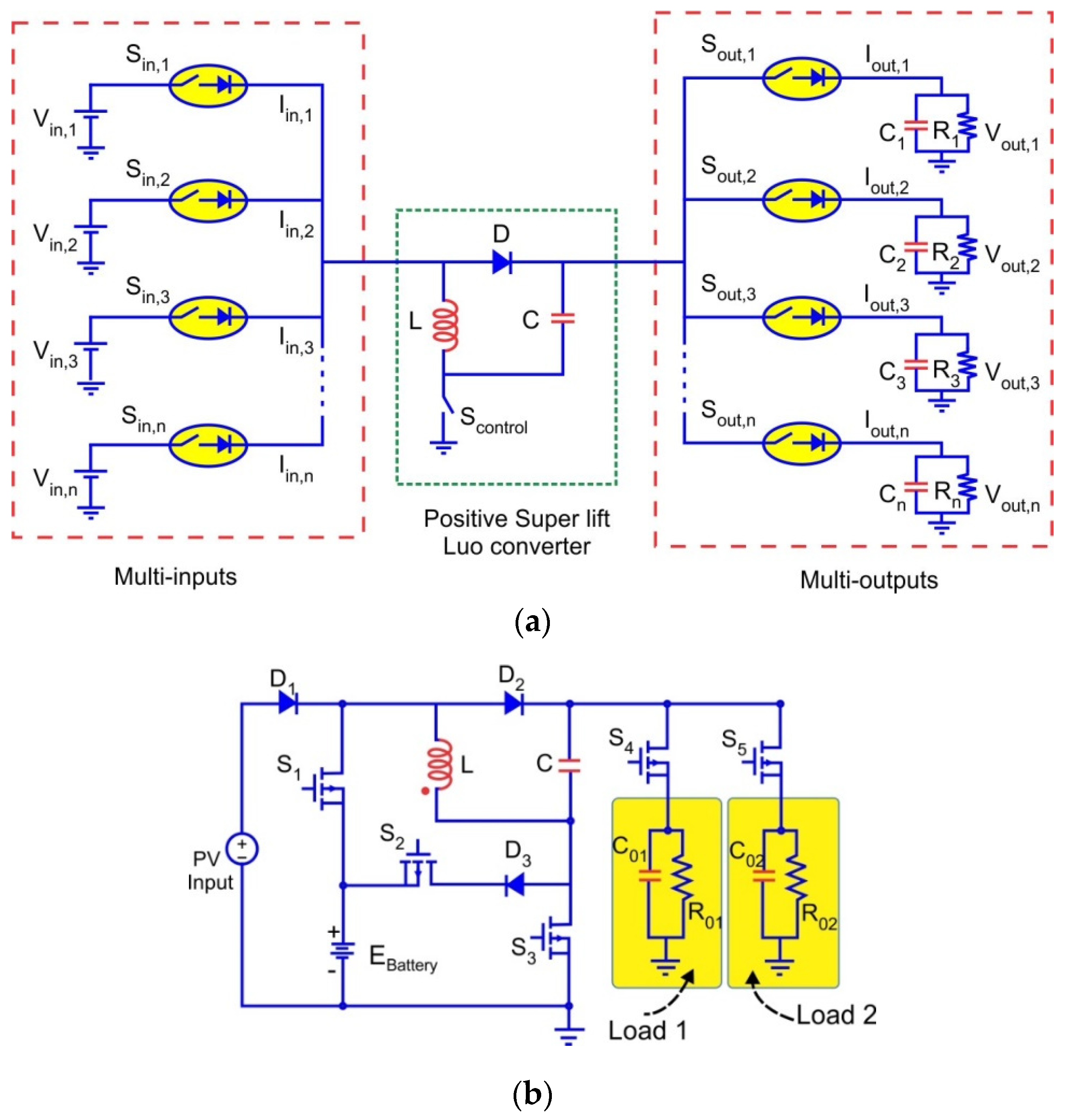
Figure 1. (a) Architecture of multi-input multi-output positive Super-Lift Luo converter (MIMO-PSLLC). (b) Dual-input dual-output (DIDO) structure of PSLLC converter.
Energies 13 06534 g001
Figure 2. Timing diagram for various modes of DIDO-PSLLC converter.
Energies 13 06534 g002
Figure 3. Equivalent circuit diagram of PSLLC converter during D1 period.
Energies 13 06534 g003
Figure 4. Equivalent circuit diagram of PSLLC converter during D2 period.
Energies 13 06534 g004
Figure 5. Equivalent circuit diagram of proposed converter during (1 − (D1 + D2)) period.
Energies 13 06534 g005
Figure 6. Bode plots of (a) controlled transfer function G11, G22 of proposed converter (b) cross-coupled transfer function G21, G12.
Energies 13 06534 g006
Figure 7. DIDO structure with input and output variable.
Energies 13 06534 g007
Figure 8. Decoupled network.
Energies 13 06534 g008
Figure 9. Flow Chart of digital model predictive controller (DMPC) Algorithm.
Energies 13 06534 g009
Figure 10. Control scheme of DMPC.
Energies 13 06534 g010
Figure 11. Flow Chart of design procedure.
Energies 13 06534 g011
Figure 12. Simulated results of higher step change at load output 1 using proportional integrative derivative (PID) controller (a) Output current I01 and I02 (b) Output voltage V01 and V02.
Energies 13 06534 g012aEnergies 13 06534 g012b
Figure 13. Simulated results of moderate step increase in load change using PID controller (a). Output current I01 and I02 (b) Output voltage V01 and V02.
Energies 13 06534 g013
Figure 14. Simulated results of moderate step decrease in load using PID controller. (a) Output current I01 and I02 (b) Output voltage V01 and V02.
Energies 13 06534 g014
Figure 15. Simulated results of higher step change at load output 1 using DMPC controller (a) Output current I01 (b) Output current I02 (c) Output voltage V01 (d) Output voltage V02.
Energies 13 06534 g015
Figure 16. Simulated results of moderate step increase in load change using DMPC controller (a) Output current I01 (b) Output current I02 (c) Output voltage V01 (d) Output voltage V02.
Energies 13 06534 g016aEnergies 13 06534 g016b
Figure 17. Simulated results of moderate step decrease in load using DMPC controller. (a) Output current I01 (b) Output current I02 (c) Output voltage V01 (d) Output voltage V02.
Energies 13 06534 g017aEnergies 13 06534 g017b
Figure 18. Hardware setup of proposed converter.
Energies 13 06534 g018
Figure 19. Case 1—Experimental results of step change at load 1.
Energies 13 06534 g019
Figure 20. Case 1—Experimental results of step change at load 1.
Energies 13 06534 g020
Figure 21. Case 2—Experimental results of step change at load 2.
Energies 13 06534 g021
Figure 22. Case 2—Experimental results of step change at load 2.
Energies 13 06534 g022
Figure 23. Case 3—Experimental results of step change input voltage.
Energies 13 06534 g023
Table 1. Summary of switching states and its modes of operation.
ModesCharging and Discharging for BatteryControl SwitchLoad SwitchesConverter ParametersRemarks
S1S2S3S4S5LC
Mode 1OFFOFFONOFFOFFChargingChargingL, C → forms a parallel connection and gets charged.
C01 and C02 → discharges to the load.
Mode 2ONOFFOFFONOFFDischargingDischargingL, C → forms a series connection and discharges to the load.
C01 → charge.
C02 → discharge to the load.
Mode 3OFFONOFFOFF ONDischarge to the load and charges the batteryDischargingL, C → discharges.
C01 → discharges to the load.
C02 → charges.
Battery → gets charged through inductor.
Table 2. Specification of Converter for simulation and prototype.
Vin (V)VB (V)L (mH)C (µF)C01 (µF)C02 (µF)Freq.
(KHz)
R1
(Ω)
R2
(Ω)
D1D2
4020168068068010025200.50.2
Table 3. Comparisons of various scenarios with PID controller and DMPC controller.
ControllerChange in Load Resistor R01 (Ω)Change in Output Current I01 (amp)Change in Output Current I02 (amp)Change in Output Voltage V01 (V)Change in Output Voltage V02 (V)Cross -Regulation
PID25–504.08–2.1174.63–4.728102.2–105.892.69–94.410.02
25–304.08–3.4454.631–4.66102.1–103.392.7–93.220.008
25–204.08–5.0214.636–4.595102.1–100.392.74–91.760.006
DMPC25–504.401–2.2332.189–2.203108.6–109.8109.4–1100.006
25–304.475–3.6712.195–2.202109.1–109.8109.4–1100.004
25–203.89–4.8893.227–3.24395.63–96.5996.65–97.310.003
Table 4. Comparisons of existing papers with the proposed converter.
S.N0Parameters[This Paper][29][23][14][15][15]
1Input Voltage40 V, 20 V24, 20 V12 V5 V5 V4.8 V
2Output Voltage103 V,
96 V
12, 8 V1.2 V, 1.5 V2.5V, 3.3V1 V, 1.5 V3.3 V,
1.2 V
3Output Power250 W35 W~0.76 W~1.5 W1.25 W0.78 W
4Control methodDigital Model Predictive controllerModel Predictive controlMultivariable PID and LQR controllerAverage current mode and charge controlDecoupling methodCross -derivative state feedback
5Switching frequency100KHz20–100 KHz10 KHz500 KHz500 KHz100KHz
6Inductor1 mH100 µH1 mH4 µH5 µH10 µH
7Capacitor680 µF220 µF220 µF10 µF10 µF10 µF
8Step change in Output Current4.401-2.233 A @I018–10 V@V20.5–1.05 A @I021 A @I01500–250 mA @I01100–200 mA @I01
4.475- 3.671 A @I010.61–0.8 A @I12–2.5 A @I021 A @I02250–500 mA @I01100–200 mA @I02
9Cross- Regulation0.006A @I020.0251.2 V @0.01s0.5 A @I020.020.03
0.004A @I02-3.3V @0.007s0.66 A @I010.010.008
10.Sensitivity0.0120.017,
0.016
0.830.050.010.01
Table 5. Comparisons of different cases of the experimental results.
Step Change in load 1t (sec)I01 (mA)V01 (V)I02 (mA)V02 (V)Cross-regulation
t1 = 10.1–0.450–49~0.1~500.001
t2 = 40.4–0.149–50~0.1~50
Step Change in load 2t (sec)I02 (mA)V02 (V)I01 (mA)V01 (V)
t1 = 10.1–0.450–49~0.1~49.80.002
t2 = 40.4–0.149–50~0.1~49.8
Input
Voltage
Variation
t (sec)Vin (V)Iin (mA)V01 (V)V02 (V)
t1 = 130–251–2~50~500.001
t2 = 5.825–302–1~50~50
Publisher’s Note: MDPI stays neutral with regard to jurisdictional claims in published maps and institutional affiliations.