1. Introduction
In the power converter circuit, the current measurement of power semiconductor devices is required for feedback control, fault detection, and soft switching. The current of power semiconductor devices is mainly measured using Rogowski coil, active current transformer, and coaxial shunt resistor.
Rogowski coil [
1,
2] is a current sensor based on electromagnetic induction. The current flowing through the conductor creates a magnetic flux. The Rogowski coil surrounds the conductor so that it is sufficiently linked with the magnetic flux. The current is estimated by applying the integrator to the voltage induced in the Rogowski coil. Because the Rogowski coil uses an air core, there is no issue due to saturation. Therefore, it has excellent linearity, provides isolation, and can measure high frequency and large current. However, the Rogowski coil is not suitable for measuring surface mount WBG devices because it must surround the conductor. In addition, in order to increase the measurement sensitivity, the number of turns of the Rogowski coil is very high, which increases the self-inductance and parasitic capacitance, thereby limiting the measurement bandwidth [
3,
4,
5].
An active current transformer [
6,
7] is a combination of a Hall effect sensor and a current transformer (CT). CT measures AC current because it is dependent on the rate of change of magnetic flux, and Hall effect sensor measures dc and low-frequency current because it is proportional to the magnitude of the magnetic field. Therefore, the active current transformer can measure from dc to high-frequency current. However, the saturation of the core limits the current rating and the design is complicated because the two measurement methods are combined. In addition, like the Rogowski coil, it is not suitable for measuring surface mount WBG devices.
Coaxial shunt resistor [
8,
9,
10] is a method of measuring current by using the voltage drop across the resistor. Because this method has a high bandwidth, it is widely used to measure the current of power semiconductor devices. In addition, the measurement accuracy of the high-frequency current is high because the shunt resistor hardly changes with frequency. However, parasitic inductance inevitably occurs due to the shunt resistor inserted in the circuit.
WBG devices, such as silicon carbide (SiC) and gallium nitride (GaN), are known to be suitable for their high efficiency and high power density, so studies have been actively conducted to apply them to power converters. However, due to the fast switching transition of WBG devices, a current sensor with a bandwidth three to five times higher than that for silicon (Si) devices and insulated-gate bipolar transistor (IGBT) devices is required for accurate current measurement [
11]. That is, the current sensor having a bandwidth of several tens of MHz is sufficient to measure the current of Si and IGBT devices, but for the current measurement of the WBG devices, these current sensors are not suitable because of their low bandwidth. In addition, WBG devices are sensitive to parasitic inductance. In particular, in the case of GaN devices, parasitic inductances can cause overshoot and ringing during switching transient [
4,
5,
12]. Therefore, although the bandwidth of the coaxial shunt resistor is high enough, it is not suitable for current measurement of WBG devices. Accordingly, PCB pattern-based pick-up coil current measurement methods that minimize parasitic inductance and have a wide bandwidth have been proposed [
5,
13,
14,
15].
In references [
5,
14,
15], a pick-up coil measurement method applying a vertical bilayer-based PCB pattern was proposed. The proposed pick-up coil is embedded in the PCB, and the current path of the device to be measure is configured outside the PCB to surround the pick-up coil. This method has the advantage of high magnetic flux linkage to the coil and high measurement sensitivity. However, since the current path is exposed to the outside, an insulator should be added between the current path and the pick-up coil, and an additional manufacturing process is required.
To overcome these problems, Wang et al. [
5] proposed a method of configuring a pick-up coil next to the device to be measured. Since this method uses a single turn pick-up coil, the mutual inductance is small, and the measurement sensitivity is low. Therefore, correction is required for accurate measurement.
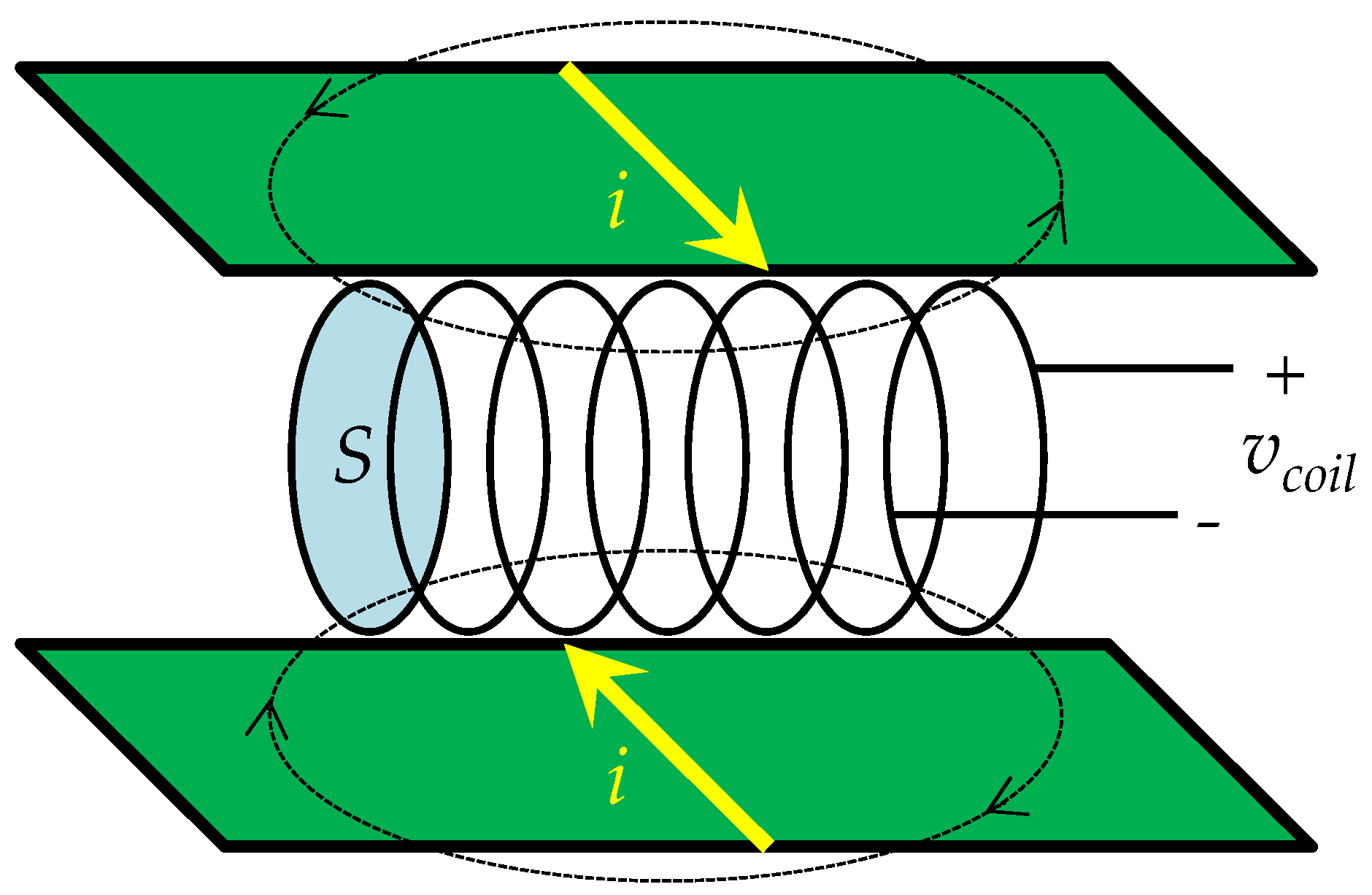
This paper proposes a PCB-embedded spiral pattern pick-up coil current measurement for WBG devices. The proposed pick-up coil can increase the number of turns by using the internal multiple layers of the PCB, which makes it possible to achieve high measurement sensitivity and mutual inductance. Since the current path is not exposed to the outside, no insulator is required between the pick-up coil and the current path. Therefore, this method is easy to manufacture and can reduce cost. To verify the performance of the proposed pick-up coil, a double pulse test (DPT) circuit is built. The measured current waveforms with the proposed pick-up coil and shunt resistor are compared.
3. Proposed Spiral Pattern Pick-Up Coil
Figure 3 shows the proposed spiral pattern pick-up coil structure. The spiral pattern pick-up coil is composed of multi-layers of PCB. The coil is configured to be wound from the outer layer to the inner layer, as shown in
Figure 3a. Because the inner layer is used,
N can be increased without increasing the area. Therefore, the spiral pattern coil has a high mutual inductance.
Figure 3b shows the spiral pattern viewed from an oblique line. If the pattern starts at layer 2, as shown in
Figure 3b, the first pattern is wound clockwise to layer 4. The second pattern is wound from layer 4 to layer 3, and the next pattern is wound from layer 3 to layer 4. The fourth pattern is wound from layer 4 to layer 2, and the four patterns are repeated.
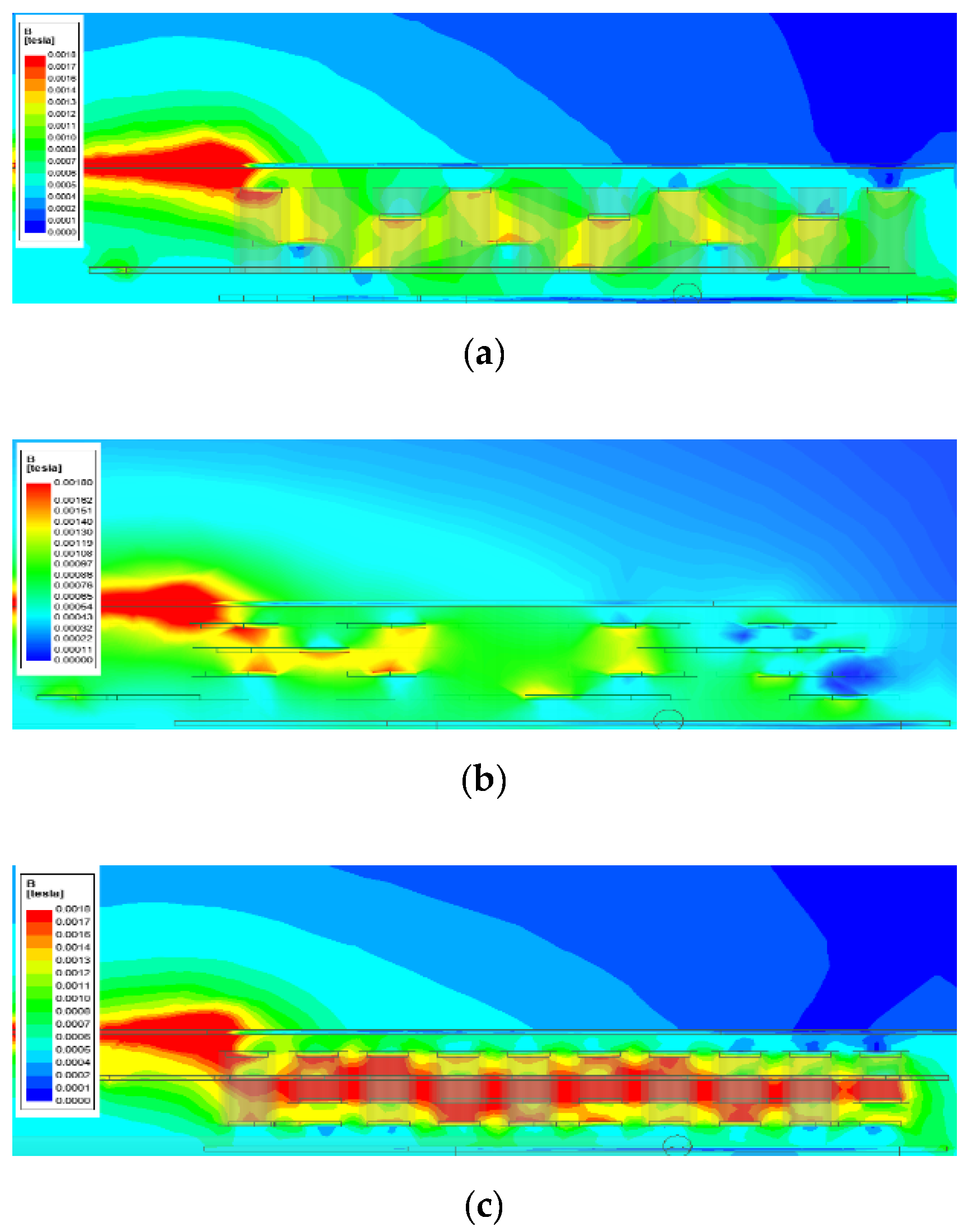
Figure 4 shows the finite element analysis of the pick-up coil applying the sawtooth pattern and spiral.
Figure 4a shows a coil configuration using the top and bottom layers without the spiral pattern.
Figure 4b shows a coil configuration using the spiral pattern. The mutual inductances according to the pattern are listed in
Table 1. The mutual inductance is simulated with the ANSYS Maxwell electromagnetic field simulation software. As shown in
Table 1, the mutual inductance of the sawtooth pattern coil is 2.75 nH, and the mutual inductance of the spiral pattern coil is 3.10 nH. By applying the spiral pattern, the mutual inductance is improved by 12% without increasing the area.
3.1. Mutual Inductance Analysis
To achieve high measurement sensitivity by applying a spiral pattern coil, it is important to increase the mutual inductance between the measurement current and the pick-up coil through an appropriate layer selection and pattern configuration. To analyze the mutual inductance of the proposed coil, we compare the mutual inductance according to the layer selection. For comparison, a six-layer PCB board is used. The top and bottom layers are modeled to flow the main current. The coil is constructed by using inner layers (layers 1–4) excluding the top and bottom layers. First, the mutual inductance of the coil, which can be constructed using two layers among the inner layers, is analyzed. Then, the mutual inductance according to the pattern is analyzed.
3.2. Analysis According to Layer Composition
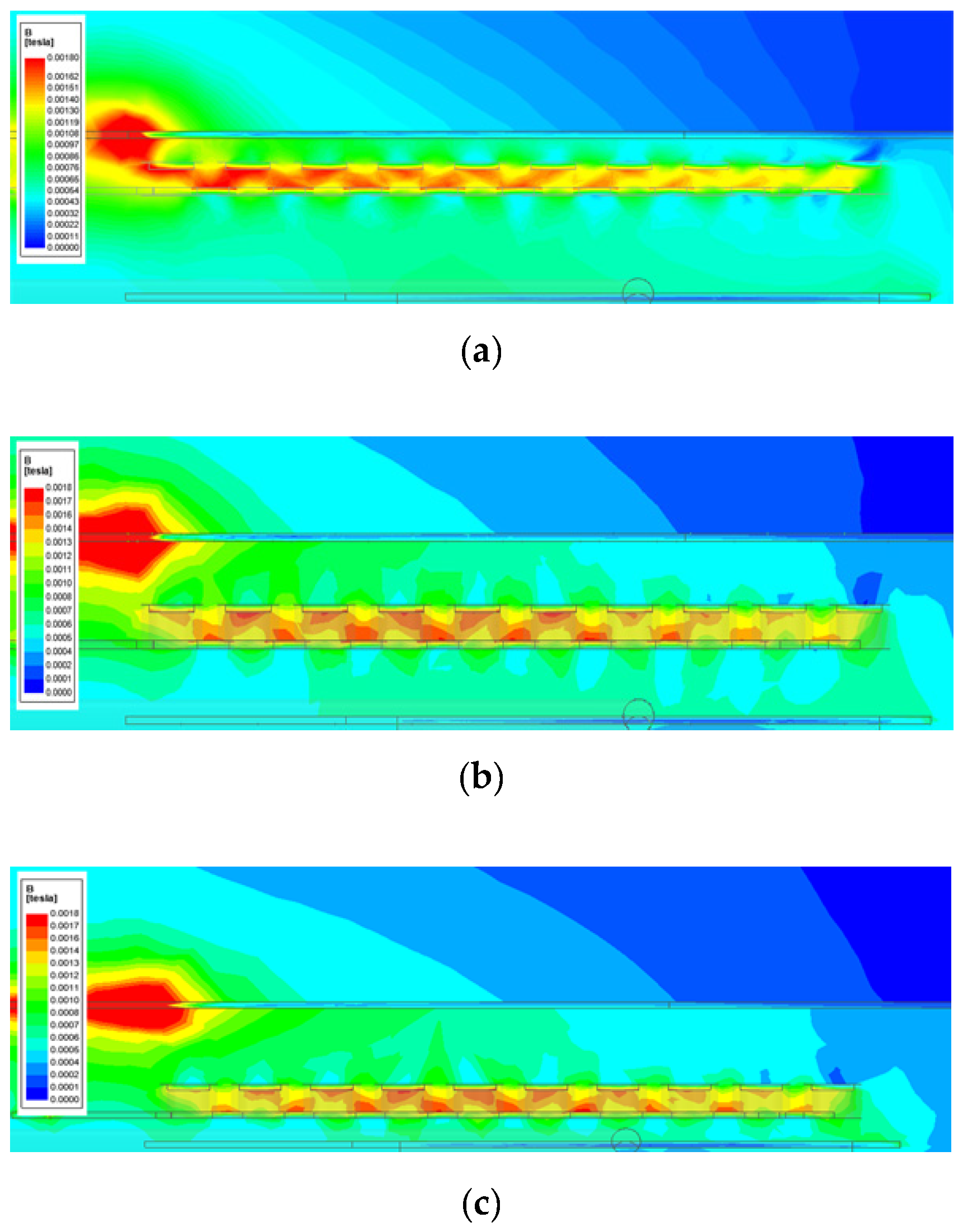
Figure 5a–c shows the coil structure using a pattern on two adjacent inner layers. The main current flows at the top and bottom layer.
Figure 5a shows the magnetic flux density distribution according to the coil configuration using adjacent layers 1 and 2. Similarly,
Figure 5b shows the magnetic flux density distribution of a coil using layers 2 and 3, and layers 3 and 4, respectively.
In the bottom layer, the current flows evenly, so the color of the magnetic flux density distribution is uniform. On the other hand, since the current path of the top layer is narrowed on the left side, the magnetic flux density distribution is strong on the left side. The amount of magnetic flux linked to the closed area of the coil is highest in the coil structure of layers 2 and 3, followed by layers 1 and 2, and layers 3 and 4. The coil structure of layers 2 and 3 has the highest mutual inductance. The coil structure of layers 2 and 3 is arranged in the center of PCB so that magnetic flux generated by the main current flowing in the top and bottom layer is uniformly linked to the coil. However, if the coil is arranged closed to the top or bottom layer, the mutual flux with the adjacent layer increases, but the mutual flux with the opposite layer decreases greatly. Therefore, the coil structure of layers 2 and 3 has the highest mutual inductance.
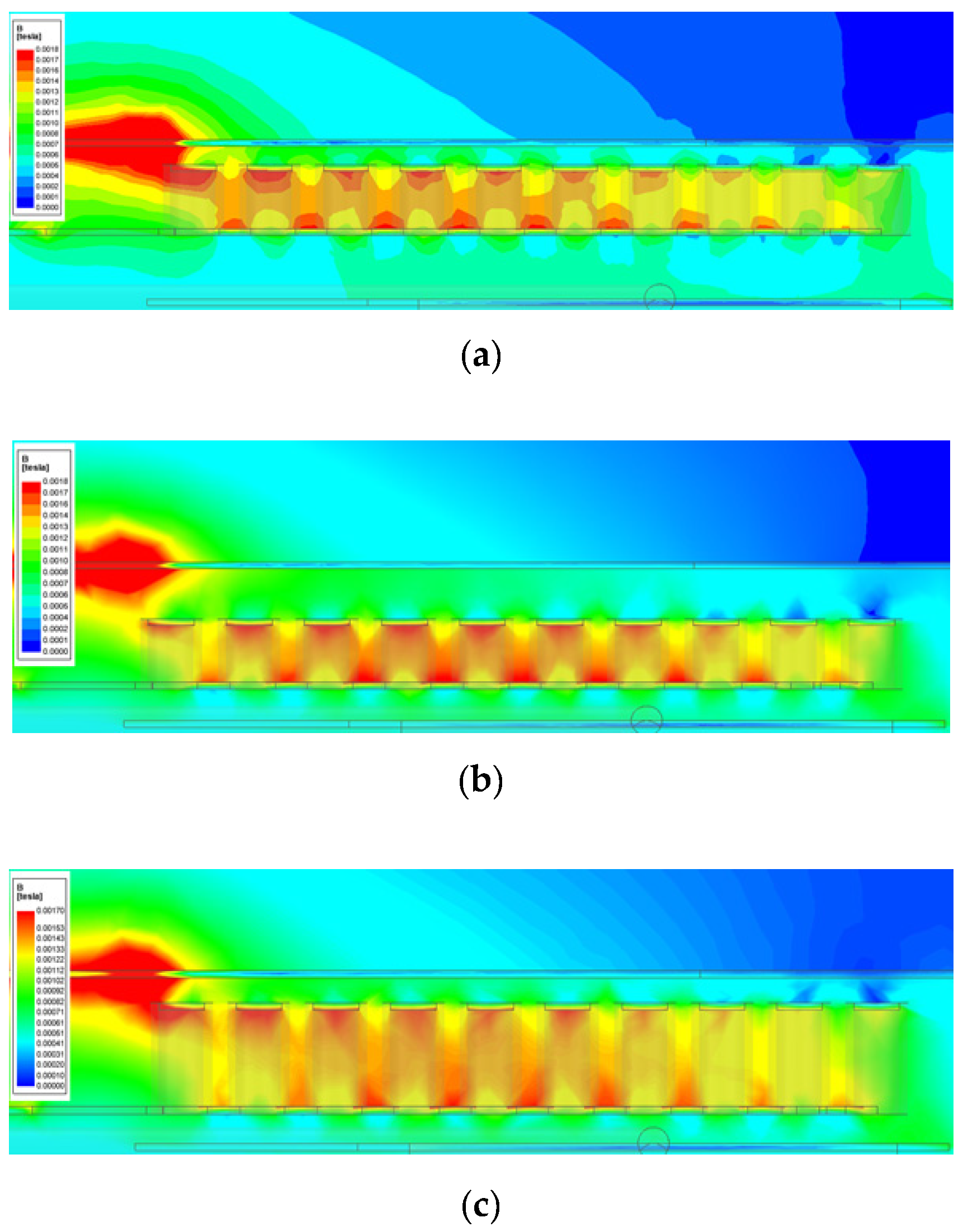
Figure 6 shows a discontinuous pattern coil, similar to the coil using two adjacent layers.
Figure 6a shows the magnetic flux density distribution of the coil using layers 1 and 3.
Figure 6b,c shows the magnetic flux density distribution of the coil using layers 2 and 4, and layers 1 and 4, respectively. The coil using layers 1 and 4 has the highest mutual inductance. This is because it has the largest closed area among the three coils, and has high mutual flux with both the top and bottom layers. The simulated mutual inductances are listed in
Table 2. The coil using layers 2 and 3 has the largest mutual inductance among the coil using two adjacent layers. The coil using layers 1 and 4 has the highest mutual inductance among the coil using non-adjacent layers. According to the simulation results, if the coil is arranged in the center of PCB and the area of the coil is large, the mutual inductance value is high. Hence, a multi-layer PCB pattern coil can have a higher mutual inductance as it can increase the number of turns by using the multiple inner layer.
3.3. Analysis According to Coil Pattern Configuration
Figure 7 shows the magnetic flux density distribution when using three different patterns applied to the spiral pattern pick-up coil. The coils are formed on the same area. The applied patterns [
18] are sawtooth, triangle, and fishbone.
Figure 7a shows the magnetic flux density distribution of the pick-up coil to which the sawtooth pattern is applied. When a sawtooth pattern is applied to multi-layer, the closed area and the number of turns of the coil are reduced compare to the coil using the top and bottom layers. Therefore, the magnetic flux density distribution decreases and the mutual inductance decreases.
Figure 7b shows the magnetic flux density distribution of the pick-up coil to which the triangle pattern is applied. If the triangle pattern coil is continuously wound, the winding directions of the coil are opposite each other, thereby canceling the induced voltage of the coil. Therefore, the number of turns is limited in the same area. In addition, the coil is not wound in the direction of the magnetic flux density, reducing the mutual inductance.
Figure 7c shows the magnetic flux density distribution of the pick-up coil to which the fishbone pattern is applied. When the coil is continuously wound, there is no space limitation between patterns for arranging vias on the same area. In addition, the winding direction of the coil is the same, so it has the highest number of turns. Therefore, the mutual flux is the highest and the mutual inductance is the highest.
Figure 8 shows the configuration and parameters of the coil using the sawtooth, triangle, and fishbone patterns. As discussed earlier, the fishbone pattern has the highest mutual inductance due to the high number of turns. Therefore, the fishbone pattern is most suitable for the spiral pattern pick-up coil.
4. Proposed Pick-Up Coil Design and Current Path
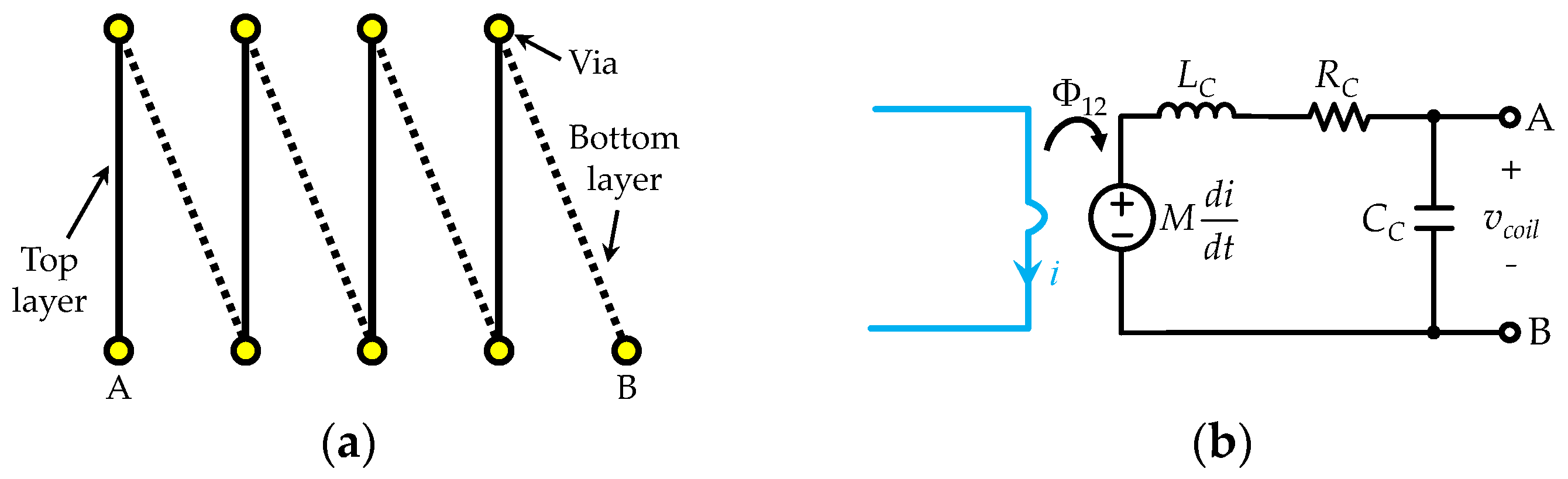
Figure 9 shows the design of the proposed spiral pattern pick-up coil. The proposed coil is implemented on the six-layer PCB. Because the space between the pattern and the via is limited, the winding width is chosen as 0.3 mm. The design is created using the Altium PCB design software.
Figure 10 shows the conversion of a model designed with Altium software to ANSYS Q3D software to extract the parameters of the coil. The self-resistance
RC, self-capacitance
CC, and self-inductance
LC of the proposed coil are simulated with Q3D. Through simulation, the parameters are found to be
RC = 0.26 Ω,
CC = 8.42 pF, and
LC = 66.29 nH, and the coil design area is 3.03 × 6.95 mm.
Figure 11 shows the current path for current measurement and the pick-up coil inside the PCB. As discussed earlier, the pick-up coil is implemented in the center of the PCB to increase the mutual inductance, as shown in
Figure 11a. The main current path is designed to flow through the top and bottom layers where the pick-up coil is not used. And the via position is designed so that current path surrounds the pick-up coil, as shown in
Figure 11b. The proposed coils are designed on inner layers 1–4. The main current path and the pick-up coil are insulated by placing clearances around the vias. Therefore, PCB-embedded pick-up coil can be manufactured without additional process work for configuring the current path.
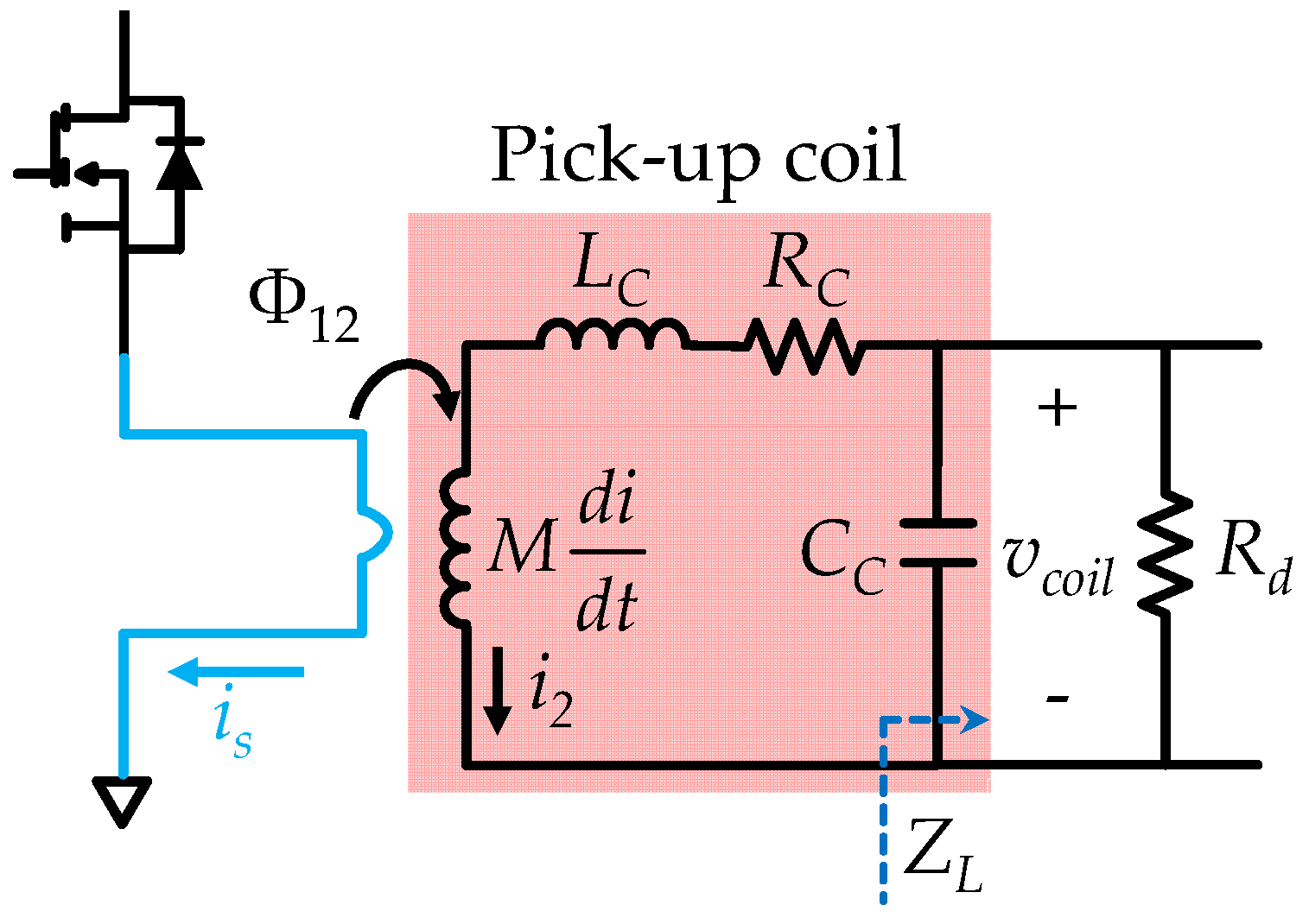
5. Pick-Up Coil Equivalent Model and Integration Circuit
Figure 12 shows an equivalent circuit of the pick-up coil.
is represents the main switch current and Φ
12 is the mutual flux.
LC,
CC, and
RC represent the self-inductance, capacitance, and resistance of the pick-up coil, respectively.
Rd represents the damping resistance and
ZL represents the output impedance of the coil.
The output voltage
vcoil of the pick-up coil is determined by the voltage divider of
vind. The primary current-to-the pick-up coil output voltage transfer function is calculated as follows:
If the damping resistance
Rd is added in parallel with the self-capacitance
Cc, we have
Substituting Equation (6) into Equation (5), we have
where
vcoil is a low, it is sensitive to the noise and ripple. Therefore, by adding the damping resistance
Rd, it is designed as the critical damping with a damping ratio of 1 without a resonance peak.
Rd is selected as 45 Ω in consideration of the parameter values extracted through Q3D and Maxwell software.
Figure 13 shows a circuit added the integrator to the pick-up coil to restore the main current. The active integrator [
19] is used, which consists of the operational amplifier (op-amp), integrator resistor
RINT, and integrator capacitor
CINT. The voltage gain of the integrator is expressed in a low-pass filter form as follows:
Combining Equations (7) and (8), the main current-to-the integrator output voltage transfer function is calculated as
where the input signal of the integrator is 0, the op-amp outputs an offset voltage. Therefore, to compensate for the offset voltage, the reset switch and feedback resistor
Rf are added in parallel to
CINT [
20].
RINT2 is the resistance of the non-inverting terminal,
IB1 is the bias current of the inverting terminal,
IB2 is the bias current of the non-inverting terminal, and
VOS is the offset voltage. When the input signal of the integrator is 0, the output voltage of the offset voltage compensation circuit is as follows:
The resistor RINT and capacitor CINT are selected in consideration of the bandwidth of the transfer function in Equation (9).
GaN HEMTs (GS66508T) are used as power semiconductor devices. The bandwidth of the sensor is calculated as
Using Equation (11), the bandwidth of the sensor is approximately 94 MHz [
21]. The bandwidth is determined according to the rise time of the GaN HEMTs. For accurate current measurement, the sensor should have a bandwidth of 94 MHz or more, and the bandwidth is designed to be 141 MHz.
If the gain is defined as
K in Equation (9), it is expressed as
RINT and
CINT. Substituting
s =
jω into Equation (9),
Gsensor is expressed as the standardized quadratic transfer function. Since the frequency at which the magnitude of the transfer function becomes −3 dB is the bandwidth, the magnitude of the transfer function is 0.707.
where
Q is the quality factor,
ωn is the natural frequency, and
ω is the bandwidth frequency.
Q = 0.5,
ωn = 1.34 × 10
9, and
ω = 141 × 10
6.
The sensor gain can be selected using Equation (12). In this paper, the gain is set to 0.1. Considering the fast charging and discharging of the capacitor,
RINT and
CINT are designed as 155 Ω and 200 pF, respectively.
Figure 14 shows the bode plot of the coil, integrator, and sensors. The bandwidth is designed to be 141 MHz.
6. Experimental Verification
To verify the proposed method, a double-pulse test (DPT) experiment was conducted.
Figure 15 shows the DPT circuit. The device under test is GaN HEMT (GS66508T). Texas Instruments OPA355 is used as an operational amplifier of the integrator. The parameter values of the pick-up coil and integrator are as specified in
Table 3.
To verify whether the proposed spiral pattern pick-up coil satisfies the bandwidth required for measuring the current of WBG HEMTs, a coaxial shunt resistor (SDN-414-10) was used for comparison. Because the shunt resistor does not change its resistance according to the frequency and has a high bandwidth, it satisfies the bandwidth required for measuring the current of a WBG device. Thus, it can be said that the shunt resistor can measure the current of the WBG device most accurately. Therefore, the current measurement performance is verified by comparing the waveform measured with the shunt resistor and the waveform measured with the pick-up coil. The integrator gain of the pick-up coil was selected to be equal to the shunt resistance, through Equation (12).
The DPT was conducted under the experimental conditions listed in
Table 4. The specifications of the shunt resistor and the design parameters of the pick-up coil are listed in
Table 4. The first pulse is injected for 5.5 μs and the second pulse is injected for 2 μs. To compare the performance of the two current sensors, the current was measured simultaneously, and the two waveforms were compared.
Figure 16 shows the output values of the shunt resistor and the proposed pick-up coil. It can be seen that the waveforms of the two current sensors are almost identical in all sections of the DPT experiment. If the offset of the actual op-amp is not compensated, the integral value due to the offset changes. Then, the rise slope of the current in the DPT waveform would be different. It can be seen indirectly that the offset compensation circuit and the reset switch are well applied.
Figure 17 shows the enlarged waveform of the transient section in which the switch turns off and on in the DPT experiment.
Figure 17a shows the waveform when the switch current turns off at 10 A, and
Figure 17b shows the waveform when the switch current turns on at 10 A. The two waveforms in
Figure 17 indicate that the current sensor using the pick-up coil tracks the shunt resistance well in the transient section, as well as over the entire DPT waveform. As shown in
Figure 17a, the falling time of the current is almost the same as that of the shunt resistor. In
Figure 17b, the rise time and peak value of the current versus the shunt resistor are almost the same.
Unfortunately, both waveforms can be seen to generate ripples, due to noise components. The pick-up coil can theoretically be called an isolated current sensor independent of the power loop. However, a coupling capacitor can be seen between the pick-up coil and the power loop. Consequently, a noise current is generated by the coupling capacitor in the transient section and a ripple is formed in the integrator output, as shown in
Figure 17. Coupling capacitors are also an important factor when designing a pick-up coil and should be considered sufficiently during the design phase.


