Abstract
This paper presents an original method of power loss validation in medium-voltage SiC MOSFET (metal–oxide–semiconductor field-effect transistor) modules of a three-phase inverter. The base of this method is a correct description of the on-state performance of the diodes and the transistors in a PWM (pulse width modulation)-controlled inverter phase leg. Combined electro-thermal calculations are applied to precisely estimate the losses in the power devices and then, to find the suitable circuit parameters of a test circuit to emulate these conditions. A simple square-wave-controlled half-bridge with an inductive load enables the electrical and thermal stresses comparable to these in the inverter, and moreover, provided equations that confirmed the possibility of balancing the load between the diodes and the transistors. The circuit with 3.3 kV SiC MOSFETs was tested to verify the impact of selected parameters on power losses with the main focus on duty ratio. The same module was applied, in addition to an inductive load (3 × 112 μH) and two sets of DC-link capacitors (750 μF), to validate a phase leg of a 220 kVA inverter. In spite of a significantly apparent power, the active power delivered from the DC supply settled around 1 kW, which was enough to emulate 390 W of losses in two transistors and diodes.
1. Introduction
Nowadays, research works on medium-voltage power conversion with silicon carbide (SiC) power devices can be divided into two substantial parts. The major interest of researchers seems to be focused on relatively new devices rated at 10 kV and more [1,2,3], mostly developed for power grid applications, where direct silicon (Si) competitors do not exist due to physical limits. On the other hand, recent literature reports also show 3.3 kV rated power modules with SiC MOSFET (metal–oxide–semiconductor field-effect transistor) and Schottky diodes, competing against well-established Si IGBTs (insulated gate bipolar transistors), usually in motor drive inverters [4,5]. The major advantage is the much faster switching of SiC unipolar devices, cutting down the amount of energy dissipated during turn-on and turn-off processes [6]. However, a comparison of the on-state performance is not that conclusive as IGBTs show a lower voltage drop at higher current ratings while SiC MOSFETs show the ability to conduct reverse currents. This issue has been already investigated in the literature, to mention only [7,8,9,10,11,12], where the performance of SiC FETs in the inverter phase leg was studied. A typical inverter leg with a standard switch based on Si IGBT requires the forward diode to carry the reverse current, while in the MOSFET–Schottky pair, the majority of this current flows through low-resistive substrate and channel. This means that the antiparallel SiC Schottky is mostly utilized during dead-time periods. Therefore, most of the existing knowledge regarding the transistor and diode pair operating inside the power module of the inverter is obsolete for SiC devices. On the base of the experiences of the authors of this paper, datasheet information describing on-state and dynamic performance show limited value in a complex electro-thermal process of medium-voltage power converter design. Moreover, a well-known double pulse test procedure can be used to verify the switching performance, however, the outcomes may vary in the final system due to the different distribution of parasitic capacitances and inductances [13]. Thus, new challenges in the design process of power converters based on medium-voltage SiC power devices generates the need to research new methods which enable continuous operation testing, without building an expensive fully scaled inverter. The main requirement is simplicity, which will be always related to low cost as all complex methods in medium voltage and high-power range require expensive set-up and equipment. The ability to accurately measure the power loss is essential as well. Previous experiences show that problems related to the measurement and the estimation of losses in power electronic converters have always been as challenging as important [14,15]. The right measurement of power losses is even harder for wide band-gap power devices, especially when higher electromagnetic interferences occur and the amount of measured losses is low. Unfortunately, the most obvious method based on input and output power measurement would require extremely precise current and voltage measurements [16], which, for medium voltage, is extremally difficult and also expensive. A number of calorimetric methods [16,17,18,19,20] enable the measurement of overall efficiency, however, dividing the power losses between passive and active elements requires additional effort, which again, for medium-voltage conditions, is challenging. Moreover, the design of the calorimetric setup for medium-voltage converters characterized by high volume is also problematic, especially when isolation requirements are taken into account. As mentioned above, electrical-based measurements may bring accurate results by double-pulse measurements [21,22] with an additional focus on measurement techniques [23], however, in the final converter the performance of the devices may differ. This issue is even more visible for medium-voltage devices as the layout of the double-pulse setup is hard to repeat in the converter, which leads to differences in the parasitic components influencing the switching behavior. In response to this issue, several methods that reflect the real conditions in power converter systems have been proposed. Most common are those derived from opposition methods [24] and use a full-bridge topology [25,26,27,28,29]. However, the design of such a system with two half-bridge modules almost equals the design of a three-phase inverter, which means complexity and high expenses. Other solutions based on DC–DC [30,31] or half-bridges can be also found [32] in the literature but they were, again, proposed for low-power SiC or GaN devices and are not suitable for medium-voltage/high-power systems, where the main problem is the power dissipation. Even for the resistive load power at a fraction of the high rated power of a medium-voltage converter, this ends in tens of kWs to dissipate in laboratory conditions.
All these works were carefully studied to find a suitable solution for a very challenging process of medium-voltage SiC inverters design and testing. As a consequence, a novel method using simple measurements in the half-bridge circuit and precise electro-thermal calculations is proposed to emulate the power losses of the module applied in a three-phase inverter. This method and their experimental validation can be counted as a main contribution of this paper. In particular, the precise equations describing on-state losses in the three-phase inverter including reverse conduction phenomenon and dead-times is provided in Section 2. Moreover, the behavior of the half-bridge with the inductive load is explained and described for the first time to provide background for precise power loss emulation in SiC MOSFETs and Schottky diodes. Section 4 presents the experimental validation of the equations presented in Section 2, by the means of power loss measurements for various voltages, switching frequencies and duty ratios, which is also an original content of this paper. Finally, a showcase of the proposed method by means of power loss estimation and validation for selected the operating point of a three-phase inverter is shown in Section 5, while Section 6 concludes the paper.
2. Power Module with SiC MOSFETs and Schottky Diodes in a Three-Phase Inverter
In contrast to low-voltage applications, medium-voltage SiC power devices operate only inside isolated power modules [1,3,4,5,6]—usually in half-bridge configuration [33,34,35]. Such a module can be a part of an isolated or non-isolated DC–DC converter, however, the most common application is a three-phase inverter composed of three pieces—see Figure 1a. For the sake of simplicity, let us consider a general case when the inverter is supplied from DC voltage source VDC and connected to three-phase inductive load (3 × LF) also including three-phase AC voltage sources (3 × VAC). Energy may be transferred in both directions and the power factor may vary between −1 (rectifier mode) and 1 (inverter mode) by means of AC current control. However, while the more complex control issues are out of the scope of this paper, due to the focus on the methods’ simplicity, a straightforward carrier-based sinusoidal PWM (pulse width modulation) method was assumed and expected to result in balanced AC currents at three-phase outputs. Under such circumstances, all six switches operate under identical conditions by means of switching and conduction losses and thus only one—the lower switch from phase A (S4 in Figure 1a)—is the subject of further consideration. To illustrate the performance the control signals and waveforms of currents in the switch (iS), the transistor (iT) and the diode (iD) are presented in Figure 1b for a power factor near unity.
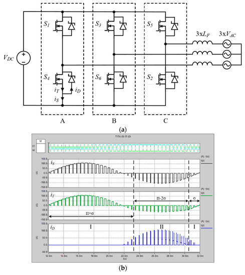
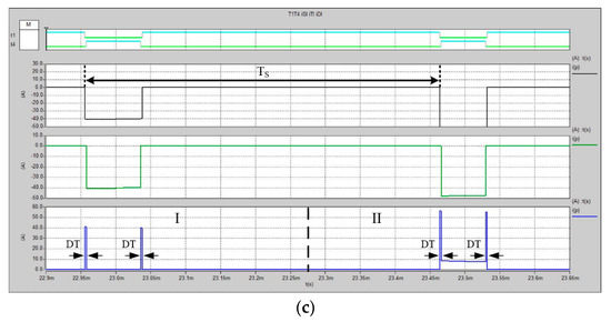
Figure 1.
Three-phase inverter (a), typical waveforms of the MOSFET (metal–oxide–semiconductor field-effect transistor) and diode currents over one fundamental period (b) and the same waveforms illustrating a border between the first and second phase (c).
2.1. Switching Losses
A well-known feature of the inverter phase leg controlled with a sinusoidal PWM method is that two switching transitions occur during period TS and the phase current always commutates within a transistor–diode pair. Therefore, after an assumption that current ripples can be neglected and the amplitude of phase currents equals to IM, switching losses of single transistor PSWT and diode PSWD operating in an inverter leg, according to the well-known relationship [36], can be described as
where fs is the switching frequency, Eon and Eoff are the energies dissipated in the transistor during the turning on and turn off processes obtained for voltage VT and current IT, while EREC is the diode switching energy. Please note that this equation assumes a linear dependence of switching energies, which for SiC MOSFETs is usually considered true.
2.2. On-State Performance
In terms of on-state performance, the SiC MOSFET/Schottky pair can be recognized as more complex than the most common solution in medium-voltage inverters which is a pair of an Si IGBT and a forward diode [7,8,9,10,11,12,13]. A closer look at the waveforms in Figure 1b shows that, in addition to conducting the current during short dead-time periods, the diodes also share a negative current of the switch with MOSFETs at some specific circuit conditions. Thus, the transistor takes the whole switch current not only during the positive sign of iS, but also in areas defined in Figure 1b by angle σ as well. The reason for such behavior is the existence of the voltage of the built-in Schottky contact VTO (relatively high in SiC, usually slightly below 1 V) and the very low on-state voltage drop VSD(ON) across the resistances of MOSFETs counted in single milliohms. When VSD(ON) < VTO, the diode is turned-off after a dead-time period under zero voltage conditions—this case can be seen in the left switching period in Figure 1c. In the next switching period, the reverse current is higher, VSD(ON) > VTO and the diode conducts in parallel to the MOSFET. As presented in [10] the angle σ is related to the phase current and parameters of the devices, specifically, and it may be described as
where rON is the on-resistance of the conducting SiC MOSFET. As a consequence, two basic areas may be distinguished as in Figure 1b:
- Area I when only the transistor is conducting (excluding dead-time periods), duration (π + 2σ);
- Area II when the transistor and diode share a negative current (π − 2σ).
Previously, the impact of the dead time on the on-state losses was neglected in the author’s works [10,37,38], however, in some operating points, it may be noticeable. Therefore, a “dead-time duty factor” γ is introduced as
where TDT is the single period of dead time (occurs two times per switching period). Using the same approach as in [10], the transistor on-state power loss for the area I can be described as
where m is the modulation index and ϕ is the phase angle between the phase voltage and current. The remaining part of the loss in the transistor is expressed as
where rD is the series resistance of the diode, Σr is the sum of rON and rD and VTO is the threshold voltage of the diode. Similarly, the diode on-state loss during the II area can be expressed as
Additional diode conduction losses during dead time are equal to [12]:
In general, the equations presented above prove that the distribution of the current among devices in the MOSFET–Schottky pair of the power module depend on circuit conditions (voltage, currents and power factor), control parameters (modulation index and dead-time duration), as well as temperature-influenced parameters of the devices.
2.3. Power Loss and Junction Temperatures Estimations
The equations presented above along with well-known thermal relationships may be applied to calculate power losses and junction temperatures of the transistors and diodes operating in a three-phase inverter. It is noteworthy that both losses and temperatures are averaged over one fundamental period of the phase current. Temperature variations, which occur in shorter time periods, will not be considered under the assumption that the thermal capacitances of medium-voltage modules and their cooling system are significant. Another simplification is an assumption of the same temperature of the common heatsink. All in all, the electrical (power loss) and thermal (temperatures) equations may be coupled in one procedure executed until the system reaches steady-state. The diagram of the procedure described more thoroughly in [10,37] is shown in Figure 2. The base for the calculations is a reference between the electrical parameters of the module and the junction temperatures described based on the datasheet and/or previously performed measurements. In the next step, the conduction (PC) and switching losses (PS) for the diodes and transistors at room temperature are determined using Equations (1)–(8) and also parameters of the three-phase inverter (phase current IM, DC-link voltage VDC, power factor cosσ, switching frequency fS, modulation index m). Then, the average junction temperatures are calculated on the basis of the thermal parameters of the module and the applied heatsink (RTHSA). The next step is to check if the system is in steady state, in particular if the rise of the junction temperatures is lower than the assumed threshold. A negative answer leads to another iteration: electrical parameters are updated according to new junction temperature values and calculations of losses and temperatures are repeated. A positive answer leads to the final results—the steady state junction temperatures of diodes and transistors for given circuit conditions.
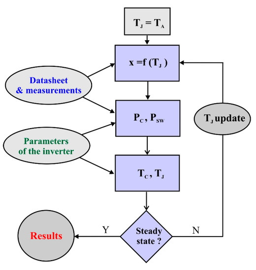
Figure 2.
The diagram of the applied procedure to estimate power losses and junction temperatures.
The described procedure was applied to estimate power losses and junction temperatures in transistors and diodes of a three-phase inverter rated at 220 kVA operating at a DC voltage of 1500 V according to the scheme shown in Figure 1a. Each phase leg is assumed to contain a 3.3 kV/450 A SiC MOSFET module from Hitachi MSM450FS33A [38], and all three modules are mounted on a common liquid-cooled heatsink (RTHSA = 15 K/kW). Switching energy values were determined on the basis of double-pulse test measurements using an in-house gate driver [38]. The calculations were performed for variable switching frequency and two different power factor values—see Figure 3. As expected, the power losses rise with the switching frequency, and slightly higher values are also observed for the unity power factor in the inverter mode (see in Figure 3a) as during the rectifier mode (see Figure 3b), diodes and transistors share more reverse current.
Figure 3.
Power losses vs. switching frequency for inverter mode (a) and rectifier mode (b)—an estimation for a 220 kVA inverter.
3. Power Losses Validation in a Half-Bridge Circuit
The method of estimating the electrical and thermal behavior of the transistors and diodes presented in the previous section is strongly influenced by the accuracy of applied data. In practice, with lower precision, a risk of the thermal runaway is increased, or, on the other hand, higher safety margins may lead to oversizing the cooling system. Obviously, the accuracy of the estimations can be elevated by the use of the double-pulse tests and measurements with curve tracers by means of more real data. However, the best verification would be a design of a full three-phase inverter or validating at least a single phase leg. It is worth noting that for the medium-voltage SiC-based systems, this is accompanied by high costs, complicated measurements, and therefore, simple methods of the electrical and thermal validation may be a better option. Therefore, a novel method using a half-bridge circuit with an inductive load is proposed to meet the expectations of medium-voltage inverters. The main idea is to reproduce the electrical and thermal conditions of the power module operating in a three-phase inverter using a simpler circuit—the square-wave controlled half-bridge with an inductive load.
The circuit (Figure 4a) and layout are similar to a single-phase of an inverter, and electrical and thermal features close to the final design can be achieved. The required amount of active power from a DC supply is limited as energy is circulating between capacitors CH/CL and load inductor L. The method is very simple—the operating conditions can be adjusted by means of the supply voltage VDC, the inductance L and the switching frequency fSH. Moreover, changes of the transistor duty ratio D decide on the precise distribution of the power losses between the transistors and diodes to precisely reproduce the conditions in a three-phase inverter, also including the reverse conduction of SiC MOSFETs. As will be presented in next sections, power loss measurements are not complex and the level of electromagnetic interferences is lower than in the inverter due to soft-switching between transistors and diodes. Finally, due to just a few necessary components (single half-bridge module, inductor, two sets of DC capacitors), also in terms of measurement equipment (power meter, cooling system), and simple open-loop control without sensors, the method can be recognized as relatively low in cost.
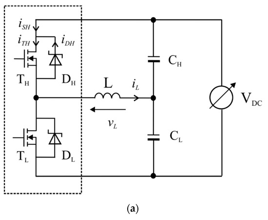
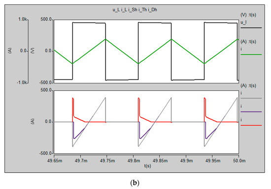
Figure 4.
Half-bridge circuit (a) and basic waveforms (b) for square-wave operation simulated in Saber.
3.1. Square Wave Controlled Half-Bridge Circuit
The half-bridge circuit presented in Figure 4a may be applied to test the performance of a medium-voltage SiC power module. There is a possibility to apply an open- or closed-loop PWM control to obtain sine current in the load inductor L to acquire conditions similar to those expected in a three-phase inverter. However, low fundamental frequency will lead to significant values of passive components. Instead, the proposed method suggests a simple square wave control at frequencies in the range of kHz to limit the necessary inductance and capacitance. At the same time, operating conditions comparable to the inverter in terms of power losses and junction temperatures can be reached. As can be seen in Figure 4b, the square wave load voltage (vL) results in a triangle waveform of the inductor current (iL) which is equally distributed among two switches. During the first half of the switching period, TSH, the rising load current flows through the upper switch TH/DH, in the other half TL/DL are in on-state.
Behavior of the upper transistor TH and diode DH can be analyzed using idealized waveforms shown in Figure 5. As an initial point, the time when an opposite transistor TL is switched off and the whole load current (amplitude IPK) is commutated to the diode DH for the dead-time period, marked as t4, is selected. Note that the transistor and diode commutate under hard-switching conditions here. Then, starting at t3, the transistor is switched on and conducts the reverse current together with the diode under the assumption that the voltage drop across the on-state resistance of the transistor rON is higher than the threshold voltage of the diode VTO. Over the time period t3, the devices share current according to [10]:
starting from ITa and IDa values (see Equations (A4) and (A5) in Appendix A). This time period refers to phase II observed for a three-phase inverter in Figure 1b. Furthermore, the time of the transistor conduction, described as a duty ratio of the transistor D’, may be influenced by changes of the dead-time, from t4 = 0 resulting in D’ = 0.5 until t4 = TSH/4 when D’ = 0.25 and reverse conduction is disabled. Another noticeable event occurs when the load current decreases to the value:
and the diode is turned-off—only the transistor is conducting reverse current (again, similarity to the area marked with the angle σ in Figure 1b can be found). Then, the load and transistor current continues to increase and finally, becomes positive after time t2. Over last time period t1, the transistor TH conducts a positive load current—it ends after TS/4 with a hard commutation to DL. Then, the cycle repeats and exactly the same waveforms can be observed for the other switch during the second half of the switching period.
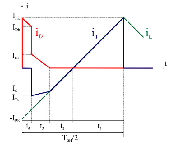
Figure 5.
Square-wave-controlled half-bridge circuit: idealized waveforms of the transistor TH (iT) and diode DH (iD) current for the first half of the switching period TSH.
Presented waveforms suggest that the majority of the current, and in consequence, conduction power losses, are dissipated in the transistor—similarly to a three-phase inverter. Moreover, the distribution of the losses between the two devices in the switch depends only on the amplitude of the load current IPK and the parameters of the diode and transistor static characteristics (rON, VTO, rD) influenced by the temperatures. Thus, there is a chance to set a given value of the power losses in either the diode or in the transistors. Even if possible, setting the precise values in both devices requires further effort. In order to change this distribution and push more losses from the transistor towards the diode, the simplest method is to adjust the length of the time t4—or, in other words, the duty ratio of the transistors:
Relations between the circuit conditions, duty ratio, static parameters of the devices and the RMS (root mean square) and average currents are collected in Appendix A, see Equations (A6)–(A15).
3.2. Method of the Inverter Power Loss Emulation
Based on the equations for the half-bridge circuit, on-state power losses in the transistor and diode may be determined (see Appendix A, Equations (A16)–(A19)). In addition, switching losses may be also easily calculated—losses occur only during the transistor turn-off process and the diode turn-on—see Figure 4. In general, the method similar to the one presented in Figure 2 may be applied here to find the power losses and junction temperatures. However, in the proposed method, the aim of such a calculation is the opposite to finding circuit conditions of the half-bridge that ensure given values of the power losses in the transistor and diode obtained from the three-phase inverter estimations. Moreover, when the cooling system is comparable to the one planned for the final inverter (3 × lower RTHSA), the same junction temperatures may be also obtained.
To sum up—the proposed method includes the following steps:
- Electro-thermal calculations for the selected operating point of a three-phase inverter according to the method presented in Figure 2, using Equations (1)–(8) to find power losses in transistor PT an diode PD.
- Calculations for the half-bridge circuit to find recommended circuit parameters of the half-bridge circuit that enables the same amount of PT and PD. Possibly, the same temperatures may also be planned.
- Apply the set of parameters to the test setup with the tested module and perform tests until the system reaches steady state.
- Measure power losses and (if possible) junction temperatures.
- Verify the results.
4. Experimental Verification of the Half-Bridge Circuit with 3.3 kV/450 A SiC MOSFET Modules
The analysis and simulations presented in previous section were verified by means of a series of advanced experiments including electrical and thermal measurements. The half-bridge circuit based on 3.3 kV/450 A SiC MOSFET modules from Hitachi (MSM450FS33A) equipped with self-made gate drivers with output voltage levels at +15/−9 V and supplementary protection circuits. The rest of the power circuit consists of 10 × 150 µF capacitors in the voltage divider and three reconfigurable 112 µH/500 A inductors acting as a passive load. Example of waveforms observed during an operation at 900 V and switching frequency fSH = 7 kHz can be seen in Figure 6b, while specific waveforms of the transistor turn-off process are shown in Figure 6c.
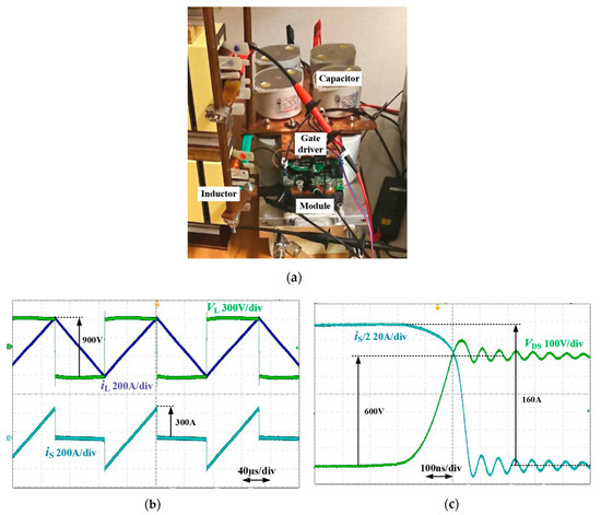
Figure 6.
Photo of the half-bridge with 3.3 kV SiC MOSFET modules (a) and the selected waveforms recorded during the operation: inductor voltage (vL) and current (iL) together with the switch current (b) half of the upper switch (transistor) current with drain-source voltage (c).
One of advantages of employing the half-bridge circuit is a simple and precise measurement of the power losses at the DC input. On the other hand, the power delivered from the DC power supply is dissipated as power loss in the power modules and also load inductors. Splitting the losses between semiconductors and magnetics neither based on electrical measurements nor employing the calorimetric chamber is simple due to, among other things, wiring and isolation issues. Therefore, power losses in the SiC MOSFET modules were calculated based on measuring the temperature and flow of the coolant.
The scheme and photo of the test setup is presented in Figure 7. In addition to the half-bridge circuit monitored by a high-precision power meter and digital oscilloscope, the substantial component is a setup monitoring temperature and flow of the coolant delivered to the heatsink by the chiller maintaining a constant liquid temperature in its buffer tank (+/− 0.5 °C). Power loss calculation is conducted by microcontroller NI MyRIO-1900 controlling the chiller and collecting data from the temperature converters and the flow meter. A preview of the circuit parameters along with the possibility to control the measurement process is possible via a PC with LabVIEW software (Figure 7b).
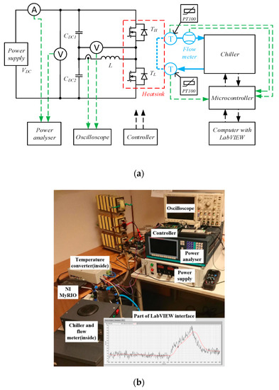
Figure 7.
Scheme (a) and photo (b) of the half-bridge measurement setup.
Such a setup enables testing the half-bridge circuit and measure the power losses in the SiC MOSFET modules and can be applied to validate equations from Section 3 at various operating points. In order to avoid damaging the modules and obtain precise results, a special procedure was used for each operating point defined by means of input voltage VDC, inductance L, switching frequency fSH and duty ratio D. At first, the calculation is performed using MATLAB to check if the module is in safe operation area by means of current, voltages, power loss and junction temperatures. Then, the half-bridge is powered and operates at selected conditions just to perform the switching energy measurements (EoffT and EonD), which are applied to repeat MATLAB calculations with experimental results. In the next step, the half-bridge circuit is pushed into continuous operation for at least 30 min to reach the thermal steady state and conduct the complete cycle of the thermal measurements. Finally, the results from the calculations can be compared with the obtained power loss value.
After checking different operating points, the procedure described above was used to verify the characteristics of the power losses versus duty ratio D’. Other parameters (VDC, L and fSH) were set as constant. It is noteworthy that this parameter shows slight influence on the total amount of power losses. Nevertheless, it will also decide about the split between diode and transistor. To illustrate this issue, a series of calculations using the procedure presented in Figure 2 was conducted in MATLAB for an exemplary case (VDC = 400 and 600 V, L = 36 μH, and fSH = 4 and 19 kHz)—see Figure 8. As expected, the decrease in the duty ratio D’ leads to an increased current in the diode and elevated losses, and at the same time losses in MOSFETs slightly drop. The results of experiments presented in Figure 8 and in Table 1 are consistent with advanced electro-thermal calculations. Operating points were chosen to test the different values of voltage, inductance and switching frequency, as well as different power levels. For all cases, the total measured losses change with the duty ratio and the maximum relative error (maxδP) was found to be below 4%. This means that the proposed method shows very good precision and can be implemented in validation of the power modules at requested power levels including an accurate split of power losses between the transistors and diodes.
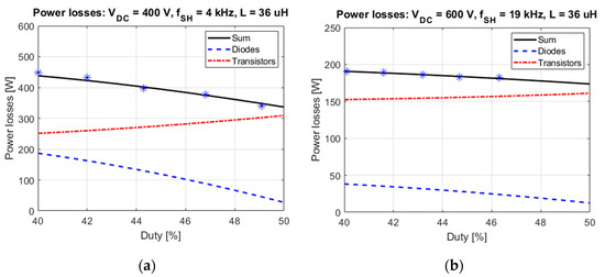
Figure 8.
Power losses in the half-bridge: transistors (red), diodes (blue) and sum of power losses in the module (black) obtained from calculations in MATLAB and experiments (stars) shown for two cases: VDC = 400 V, fSH = 4 kHz (a) and VDC = 600 V, fSH = 19 kHz (b).

Table 1.
Results for all measurement series carried out for different operating points.
5. Experimental Validation of Power Loss in Three-Phase Inverter Using the Half-Bridge Circuit
In the final section, an example of power loss validation is presented by means of experiments in the half bridge circuit. In reference to the datasheet parameters of the available power modules (MSM450FS33A), a case of the three-phase inverter rated at 220 kVA was investigated for input voltage VDC = 1500 V, switching frequency fS = 2.5 kHz, dead-time period TDT = 4 µs and unity power factor. According to the procedure described in Section 3.2, the first step is to calculate the power losses in transistors and diodes—here the characteristics presented in Figure 3b were used to find that PT = 170 W and PD = 25 W. It is noteworthy that the accuracy of calculations has been improved as a result of applying double pulse measurements in MATLAB [37] instead of datasheet values.
The next step was to find a set of half-bridge circuit parameters (input voltage VDC, load inductance L, switching frequency fS and duty ratio D) enabling the same values of losses in transistors and diodes. Theoretically, the equations presented in Section 3 and Appendix A offer a wide range of possibilities in terms of electrical parameters as the required PT and PD can be obtained in an infinite number of settings. However, the limitation is a maximum DC voltage (<1800 V for tested modules) and the switching frequency, which is restricted bythe delays in the gate driver circuit. Nonetheless, the main issue comes in a form of load inductors accessibility—here three inductors were available. Another observation is that the total losses are influenced by voltage, inductance and switching frequency while duty ratio decides about the split between the diode and the transistor. Taking the above into account, the following parameters were proposed to test the single phase leg in the half-bridge circuit with inductive load: VDC = 600 V, L = 36 µH, fS = 7 kHz and D = 48.9%. Calculations in MATLAB confirmed that for assumed heatsink parameters (RTHSA = 35 K/kW), expected levels of PT and PD will be dissipated in the SiC MOSFETs and Schottky diodes of the power module.
Then, a series of laboratory measurements were performed using the setup described in Section 4, for the assumed parameters the RMS current in the load inductors was measured to be 172 A RMS (298 A peak). It corresponds to 1032 W observed at the input by a precise power meter. This value is rather useful for overall system monitoring due to unknown loss in the inductors. The electro-thermal measurements confirmed that the power losses in the whole power module (two transistors and two diodes), further dissipated in the liquid-cooled heatsink, were at the level of 391 W (Figure 9). During such a test, it is not possible to find the split of the power losses between the diode and the MOSFET, however, further measurements of total losses for decreased duty ratio (Figure 9) were in very good agreement with the calculations. Thus, it is very likely that not only the assumed amount of losses was applied to the whole power module but also specifically to the following transistors and diodes to obtain the same electrical and thermal conditions as in a three-phase inverter.
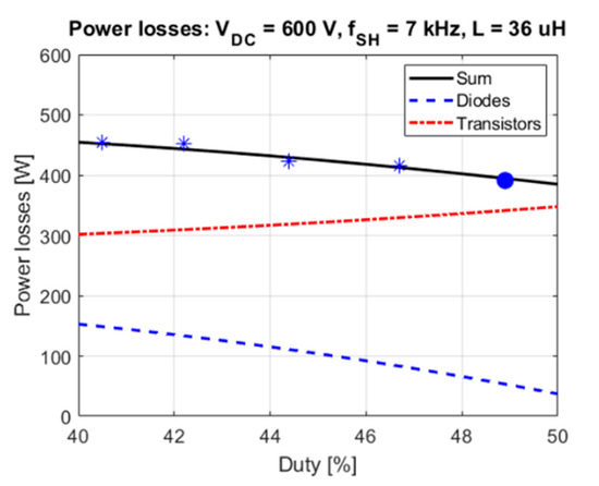
Figure 9.
Power losses in the half-bridge: transistors (red), diodes (blue) and the sum of power losses in the module (black) obtained from calculations in MATLAB and experiments (blue dot and stars).
6. Conclusions
In response to a series of problems in proper design of three-phase inverters with medium-voltage SiC MOSFET modules, a new method of power losses validation was presented in this paper. The method is based on accurate equations describing on-state losses in a three-phase inverter, and also, a half-bridge circuit loaded with an inductor. Combined electro-thermal calculations are applied to estimate power losses in the transistors and diodes of the inverter and then, to find suitable circuit parameters of the half-bridge circuit appropriate to emulate these conditions. The experimental part of the method is reduced only to tests of such a circuit with simple square-wave control. Huge amounts of reactive power circulate between DC-link capacitors and inductors to apply the assumed amount of power losses. It is important that the provided equations enable the precise emulation of power losses in the module and also in specific devices—this feature has been confirmed via a series of measurements using 3.3 kV/450 A SiC MOSFET. The same module was applied, in addition to an inductive load and two sets of DC-link capacitors, to validate the case of a 220 kVA inverter. What is especially valuable, is that the necessary power supply is limited. Slightly above 1 kW is sufficient to test a single power module operating under conditions comparable to a full scale inverter. In addition to the simple setup reducing the cost, this may be counted as a major advantage of the proposed method.
Author Contributions
J.R. proposed the main concept and the methodology. H.S. was the main contributor with regard to the theoretical analysis and the experimental setup. R.K., P.T. and G.W. contributed to the experimental study and further data analysis. Supervision, project administration, funding acquisition—J.R. All authors have contributed to the writing of the paper. All authors have read and agreed to the published version of the manuscript.
Funding
This research was funded by National Science Center, Poland project no. 2017/27/B/ST7/00970.
Conflicts of Interest
The authors declare no conflict of interest.
Appendix A
Assuming the linear rise of the load current:
Transistor and diode current can be expressed as
This leads to equations describing RMS currents of the transistor:
And the diode:
References
- DiMarino, C.; Boroyevich, D.; Burgos, R.; Johnson, M.; Lu, G.Q. Design and development of a high-density, high-speed 10 kV SiC MOSFET module. In Proceedings of the 2017 19th European Conference on Power Electronics and Applications (EPE’17 ECCE Europe), Warsaw, Poland, 11–14 September 2017; pp. 1–10. [Google Scholar]
- Zhang, L.; Ji, S.; Gu, S.; Huang, X.; Palmer, J.; Giewont, W.; Tolbert, L.M. Design Considerations of High-Voltage-Insulated Gate Drive Power Supply for 10 kV SiC MOSFET in Medium-Voltage Application. In Proceedings of the 2019 IEEE Applied Power Electronics Conference and Exposition (APEC), Anaheim, CA, USA, 17–21 March 2019; pp. 425–430. [Google Scholar]
- Parashar, S.; Kumar, A.; Bhattacharya, S. High Power Medium Voltage Converters Enabled by High Voltage SiC Power Devices. In Proceedings of the 2018 International Power Electronics Conference (IPEC-Niigata 2018—ECCE Asia), Niigata, Japan, 4–8 April 2018; pp. 3993–4000. [Google Scholar]
- Marzoughi, A.; Wang, J.; Burgos, R.; Boroyevich, D. Characterization and Evaluation of the State-of-the-Art 3.3-kV 400-A SiC MOSFETs. IEEE Trans. Ind. Electron. 2017, 64, 8247–8257. [Google Scholar] [CrossRef]
- Gill, L.; Ikari, T.; Kai, T.; Li, B.; Ngo, K.; Dong, D. Medium Voltage Dual Active Bridge Using 3.3 kV SiC MOSFETs for EV Charging Application. In Proceedings of the 2019 IEEE Energy Conversion Congress and Exposition (ECCE), Baltimore, MD, USA, 29 September–3 October 2019; pp. 1237–1244. [Google Scholar]
- Ionita, C.; Nawaz, M.; Ilves, K.; Iannuzzo, F. Comparative assessment of 3.3kV/400A SiC MOSFET and Si IGBT power modules. In Proceedings of the 2017 IEEE Energy Conversion Congress and Exposition (ECCE), Cincinnati, OH, USA, 1–5 October 2017; pp. 1343–1349. [Google Scholar]
- Ozpineci, B.; Tolbert, L.M.; Islam, S.K.; Hasanuzzaman, M. Effects of silicon carbide (SiC) power devices on HEV PWM inverter losses. IECON’01. In Proceedings of the 27th Annual Conference of the IEEE Industrial Electronics Society (Cat. No.37243), Denver, CO, USA, 29 November–2 December 2001; Volume 2, pp. 1061–1066. [Google Scholar]
- Fonteneau, X.; Morel, F.; Buttay, C.; Morel, H.; Lahaye, P. Predicting static losses in an inverter-leg built with SiC normally-off JFETs and SiC diodes. In Proceedings of the Twenty-Eighth Annual IEEE Applied Power Electronics Conference and Exposition (APEC), Long Beach, CA, USA, 17–21 March 2013; pp. 2636–2642. [Google Scholar]
- Jordan, J.; Esteve, V.; Sanchis-Kilders, E.; Dede, E.J.; Maset, E.; Ejea, J.B.; Ferreres, A. A comparative performance study of a 1200 V Si and SiC MOSFET intrinsic diode on an induction heating inverter. IEEE Trans. Power Electron. 2014, 29, 2550–2562. [Google Scholar] [CrossRef]
- Rąbkowski, J.; Płatek, T. Comparison of the power losses in 1700V Si IGBT and SiC MOSFET modules including reverse conduction. In Proceedings of the European Conference on Power Electronics and Applications, EPE 2015, Geneva, Switzerland, 8–10 September 2015; pp. 1–10. [Google Scholar]
- Yin, S.; Tseng, K.; Tong, C.; Simanjorang, R.; Gajanayake, C.; Gupta, A.K. A 99% efficiency SiC three-phase inverter using synchronous rectification. In Proceedings of the 2016 IEEE Applied Power Electronics Conference and Exposition (APEC), Long Beach, CA, 20–24 March 2016; pp. 2942–2949. [Google Scholar]
- Yin, S.; Liu, Y.; Liu, Y.; Tseng, K.J.; Pou, J.; Simanjorang, R. Comparison of SiC Voltage Source Inverters Using Synchronous Rectification and Freewheeling Diode. IEEE Trans. Ind. Electron. 2018, 65, 1051–1061. [Google Scholar] [CrossRef]
- Nayak, P.; Hatua, K. Parasitic Inductance and Capacitance-Assisted Active Gate Driving Technique to Minimize Switching Loss of SiC MOSFET. IEEE Trans. Ind. Electron. 2017, 64, 8288–8298. [Google Scholar] [CrossRef]
- Xiao, C.; Chen, G.; Odendaal, W.G. Overview of power loss measurement techniques in power electronics systems. IEEE Trans. Ind. Appl. 2007, 43, 657–664. [Google Scholar] [CrossRef]
- Fuchs, F.W.; Schroder, J.; Wittig, B. State of the technology of power loss determination in power converters. In Proceedings of the 2013 15th European Conference on Power Electronics and Applications (EPE), Lille, France, 2–6 September 2013; pp. 1–10. [Google Scholar]
- Aarniovuori, L.; Musikka, T.; Kosonen, A.; Niemelä, M.; Pyrhönen, J. Three alternative methods to determine voltage source converter losses. In Proceedings of the 2015 17th European Conference on Power Electronics and Applications (EPE’15 ECCE-Europe), Geneva, Switzerland, 8–10 September 2015; pp. 1–10. [Google Scholar]
- Christen, D.; Badstuebner, U.; Biela, J.; Kolar, J.W. Calorimetric power loss measurement for highly efficient converters. In Proceedings of the 2010 International Power Electronics Conference—ECCE Asia—IPEC, Sapporo, Japan, 21–26 June 2010; pp. 1438–1445. [Google Scholar]
- Bolte, S.; Wohlrab, L.; Afridi, J.K.; Fröhleke, N.; Böcker, J. Calorimetric measurement of wide-bandgap semiconductors switching losses. In Proceedings of the PCIM Europe 2017—International Exhibition and Conference for Power Electronics Intelligent Motion Renewable Energy and Energy Management, Nuremberg, Germany, 16–18 May 2017; pp. 1–6. [Google Scholar]
- Rothmund, D.; Bortis, D.; Kolar, J.W. Accurate Transient Calorimetric Measurement of Soft-Switching Losses of 10-kV SiC mosfets and Diodes. IEEE Trans. Power Electron. 2018, 33, 5240–5250. [Google Scholar] [CrossRef]
- Anurag, A.; Acharya, S.; Prabowo, Y.; Gohil, G.; Kassa, H.; Bhattacharya, S. An accurate calorimetric method for measurement of switching losses in silicon carbide (SiC) MOSFETs. In Proceedings of the 2018 IEEE Applied Power Electronics Conference and Exposition (APEC), San Antonio, TX, USA, 4–8 March 2018; pp. 1695–1700. [Google Scholar]
- Zhang, Z.; Guo, B.; Wang, F.F.; Jones, E.A.; Tolbert, L.M.; Blalock, B.J. Methodology for Wide Band-Gap Device Dynamic Characterization. IEEE Trans. Power Electron. 2017, 32, 9307–9318. [Google Scholar] [CrossRef]
- Ghosh, A.; Ho, C.N.M.; Prendergast, J. A Cost-effective Compact Automatic Testing System for Dynamic Characterization of Power Semiconductor Devices. In Proceedings of the 2019 IEEE Energy Conversion Congress and Exposition (ECCE), Baltimore, MD, USA, 29 September–3 October 2019; pp. 2026–2032. [Google Scholar]
- Oyarbide, E.; Bernal, C.; Molina-Gaudó, P. New Current Measurement Procedure Using a Conventional Rogowski Transducer for the Analysis of Switching Transients in Transistors. IEEE Trans. Power Electron. 2017, 32, 2490–2492. [Google Scholar] [CrossRef]
- Forest, F.; Huselstein, J.J.; Faucher, S.; Elghazouani, M.; Ladoux, P.; Meynard, T.A.; Turpin, C. Use of opposition method in the test of high-power electronic converters. IEEE Trans. Ind. Electron. 2006, 53, 530–541. [Google Scholar] [CrossRef]
- Brandelero, J.; Cougo, B.; Meynard, T.; Videau, N. A non-intrusive method for measuring switching losses of GaN power transistors. In Proceedings of the IECON 2013—39th Annual Conference of the IEEE Industrial Electronics Society, Vienna, Austria, 10–13 November 2013; pp. 246–251. [Google Scholar]
- Wechsler, M.; Simon, M.; Edler, S.; Pforr, J. A simple technique to measure the semiconductor switching and conduction losses of inverters at specified chip temperatures. In Proceedings of the 2015 IEEE Energy Conversion Congress and Exposition (ECCE), Montreal, QC, Canada, 20–24 September 2015; pp. 6594–6601. [Google Scholar]
- Kadavelugu, A.; Suryanarayana, H.; Liu, L.; Pan, Z.; Belcastro, C.; Paatero, E. A simple and accurate efficiency measurement method for power converters. In Proceedings of the 2017 IEEE Applied Power Electronics Conference and Exposition (APEC), Tampa, FL, USA, 26–30 March 2017; pp. 3265–3270. [Google Scholar]
- Lu, J.L.; Qiu, Y.; Chen, D. A full power emulation platform for evaluating power semiconductors. In Proceedings of the 2018 IEEE Applied Power Electronics Conference and Exposition (APEC), Anaheim, CA, USA, 17–21 March 2018; pp. 2861–2867. [Google Scholar]
- Stella, F.; Pellegrino, G.; Armando, E.; Daprà, D. Advanced testing of SiC power MOSFET modules for electric motor drives. In Proceedings of the 2017 IEEE International Electric Machines and Drives Conference (IEMDC), Miami, FL, USA, 21–24 May 2017; pp. 1–8. [Google Scholar]
- Biswas, S.; Reusch, D.; de Rooij, M.; Neville, T. Evaluation of measurement techniques for high-speed GaN transistors. In Proceedings of the 2017 IEEE 5th Workshop on Wide Bandgap Power Devices and Applications (WiPDA), Santa Ana Pueblo, NM, USA, 30 October–1 November 2017; pp. 105–110. [Google Scholar]
- Keuck, L.; Jabbar, N.; Schafmeister, F.; Böcker, J. Switching Loss Characterization of Wide Band-Gap Devices by an Indirect Identification Methodology. In Proceedings of the 2018 20th European Conference on Power Electronics and Applications (EPE’18 ECCE Europe), Riga, Latvia, 17–21 September 2018. [Google Scholar]
- Costa, P.B.; Silva, J.F.; Pinto, S.F. Experimental evaluation of SiC MOSFET and GaN HEMT losses in inverter operation. In Proceedings of the IECON 2019-45th Annual Conference of the IEEE Industrial Electronics Society, Lisbon, Portugal, 14–17 October 2019; Volume 1, pp. 6595–6600. [Google Scholar]
- Ishigaki, T.; Hayakawa, S.; Murata, T.; Nozoe, T.; Onose, H.; Miki, H.; Takayanagi, Y. 3.3 kV/450 A Full-SiC nHPD2 (next High Power Density Dual) with Smooth Switching. In Proceedings of the PCIM Europe 2017; International Exhibition and Conference for Power Electronics, Intelligent Motion, Renewable Energy and Energy Management, Nuremberg, Germany, 16–18 May 2017; pp. 1–6. [Google Scholar]
- Hayes, J.; Curbow, W.A.; Sparkman, B.; Martin, D.; Olejniczak, K.; Wijenayake, A.; McNutt, T. Dynamic Characterization of Next Generation Medium Voltage (3.3 kV, 10 kV) Silicon Carbide Power Modules. In Proceedings of the PCIM Europe 2017; International Exhibition and Conference for Power Electronics, Intelligent Motion, Renewable Energy and Energy Management, Nuremberg, Germany, 16–18 May 2017; pp. 1–7. [Google Scholar]
- Negishi, T.; Tsuda, R.; Ota, K.; Iura, S.; Yamaguchi, H. 3.3 kV All-SiC Power Module for Traction System Use. In Proceedings of the PCIM Europe 2017; International Exhibition and Conference for Power Electronics, Intelligent Motion, Renewable Energy and Energy Management, Nuremberg, Germany, 16–18 May 2017; pp. 1–6. [Google Scholar]
- Bierrhoff, M.H.; Fuchs, F.W. Semiconductor Losses in Voltage and Current Source IGBT Converters Based on Analytical Derivation. In Proceedings of the 2004 IEEE 35th Annual Power Electronics Specialists Conference, Aachen, Germany, 20–25 June 2004; pp. 2836–2842. [Google Scholar]
- Rabkowski, J.; Płatek, T. A study on power losses of the 50 kVA SiC converter including reverse conduction phenomenon. Bull. Pol. Acad. Sci. Tech. Sci. 2016, 64, 1–8. [Google Scholar] [CrossRef][Green Version]
- Rabkowski, J.; Sobieski, R.; Zdanowski, M.; Piasecki, S. 3.3 kV/450 a SiC MOSFET Module—Modelling and Experiments. In Proceedings of the 20th European Conference on Power Electronics and Applications, Riga, Latvia, 17–21 September 2018; pp. 1–10. [Google Scholar]


© 2020 by the authors. Licensee MDPI, Basel, Switzerland. This article is an open access article distributed under the terms and conditions of the Creative Commons Attribution (CC BY) license (http://creativecommons.org/licenses/by/4.0/).