Mechanical Degradation Analysis of an Amorphous Silicon Solar Module


Abstract
1. Introduction
2. Materials and Methods
2.1. Sample Preparation
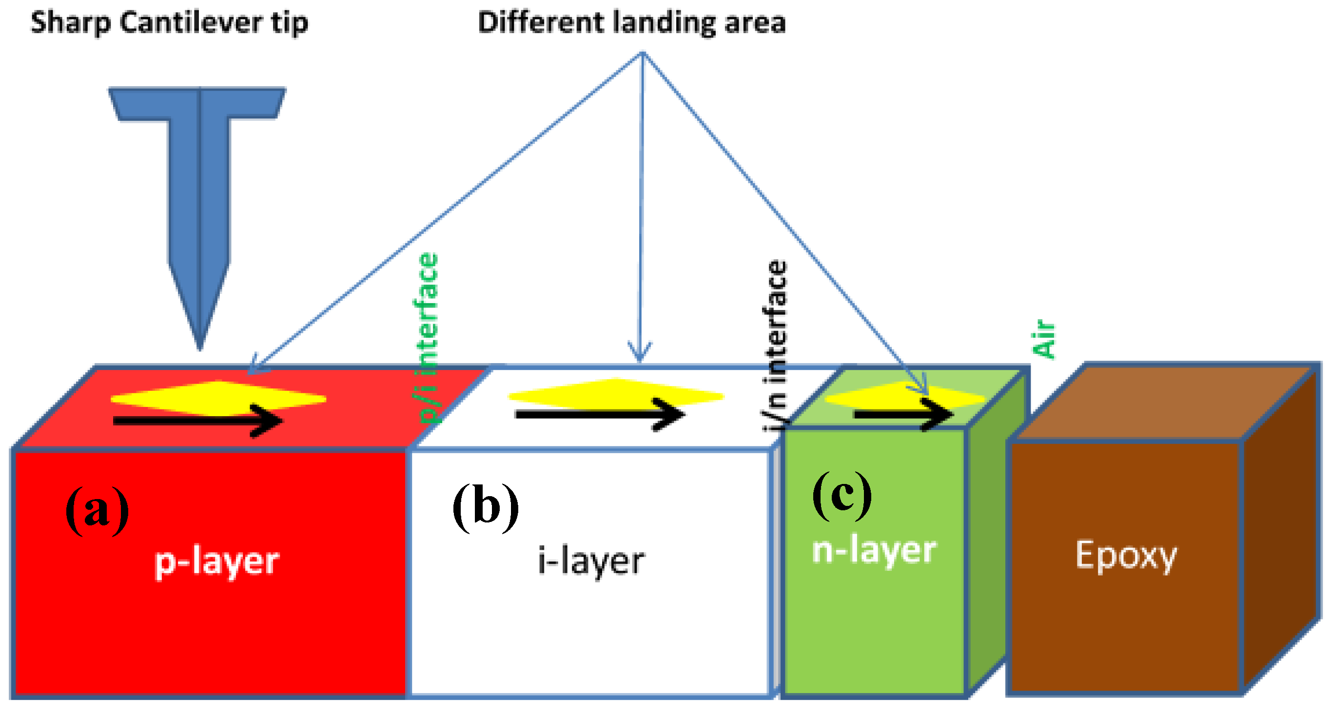
2.2. Towards Reaching the p-Si:H/i-Si:H/n-Si:H Interfaces
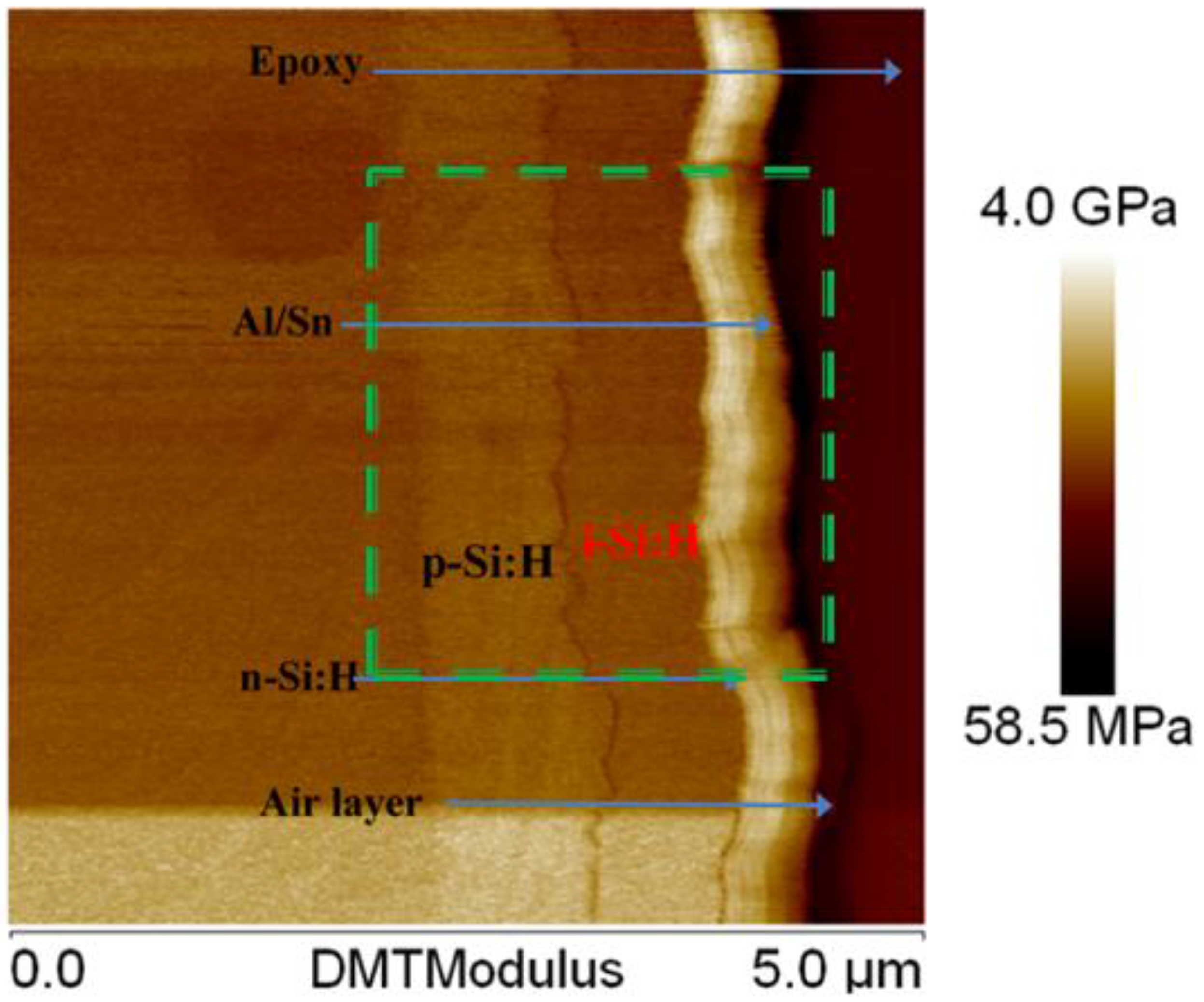
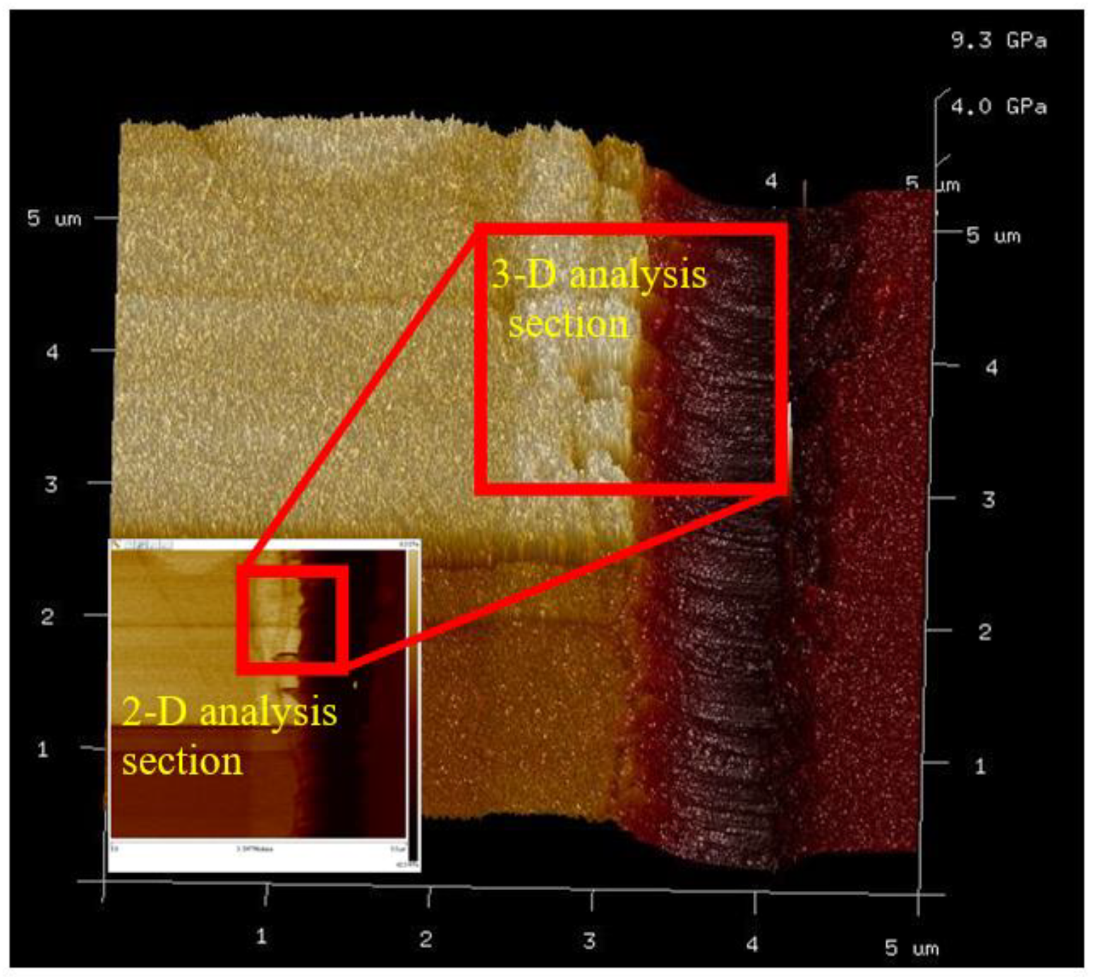
2.3. Identification of Interfacial Locations Using Force Quantitative Nano-Mechanical (PF-QNM)
2.4. Identification of Various Interfaces
3. Results
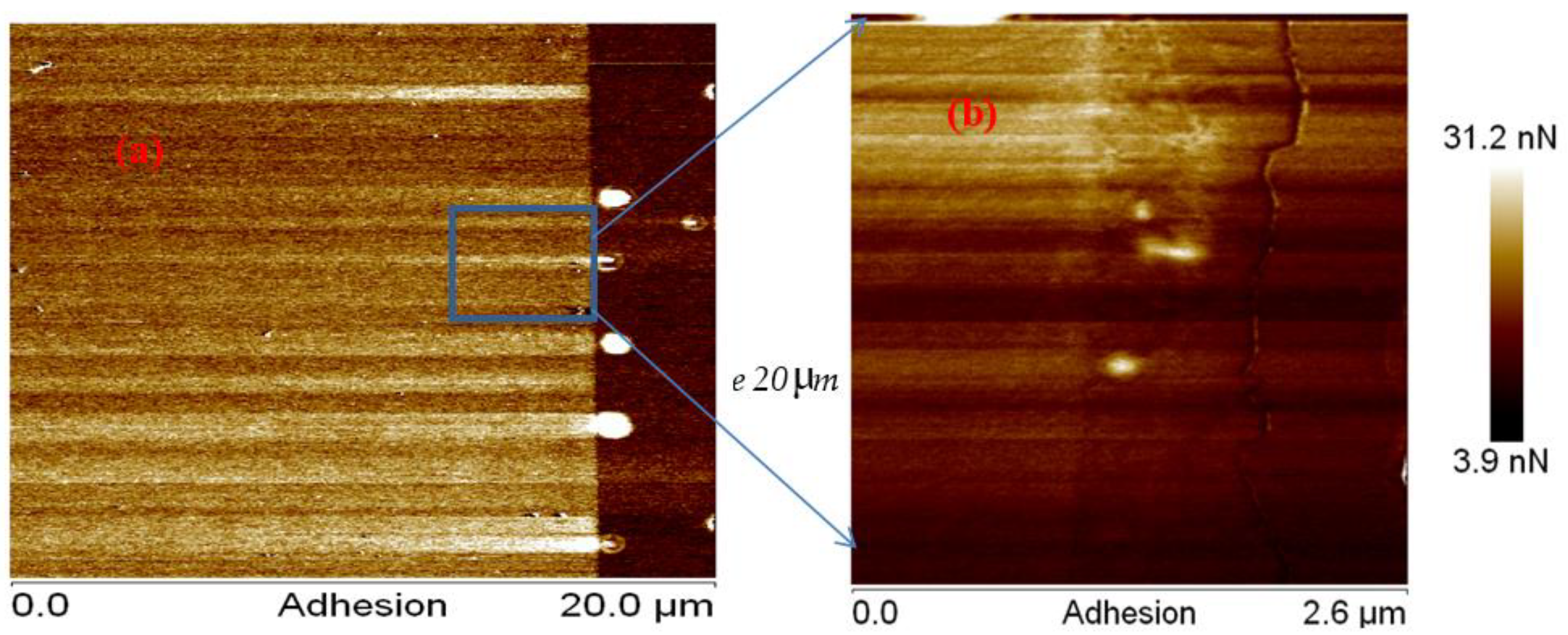
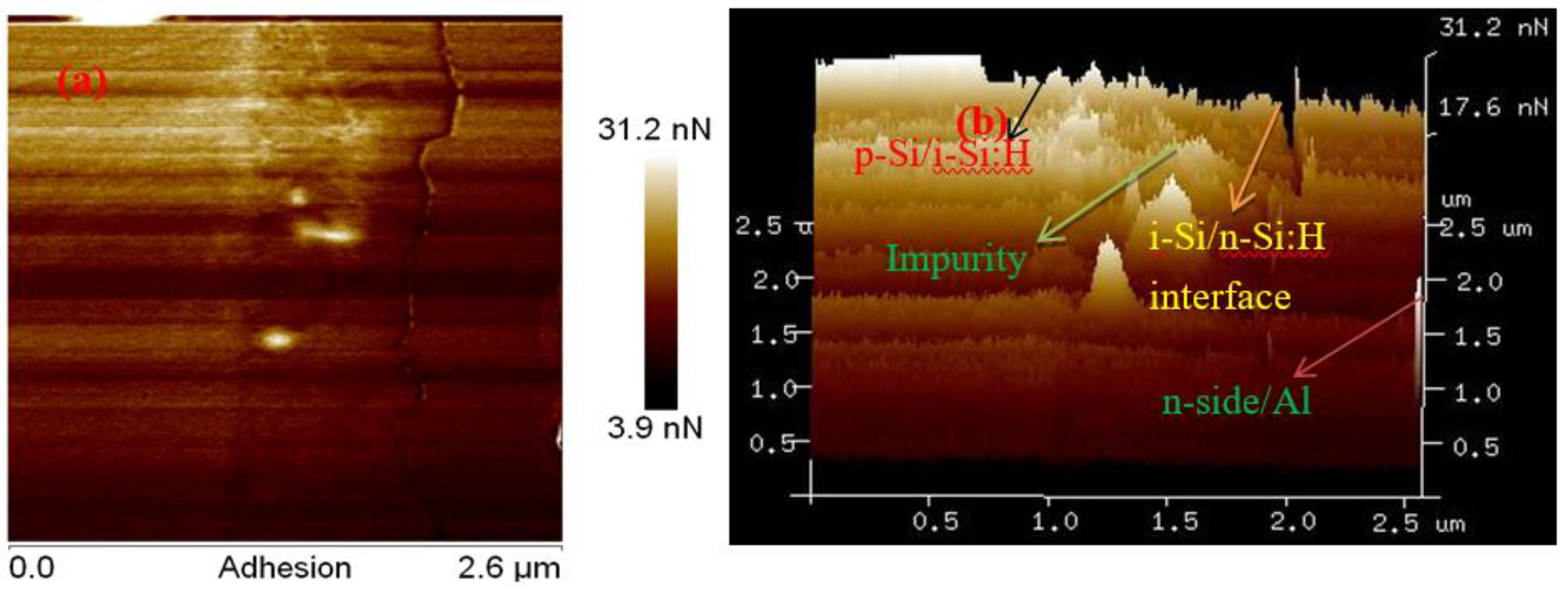
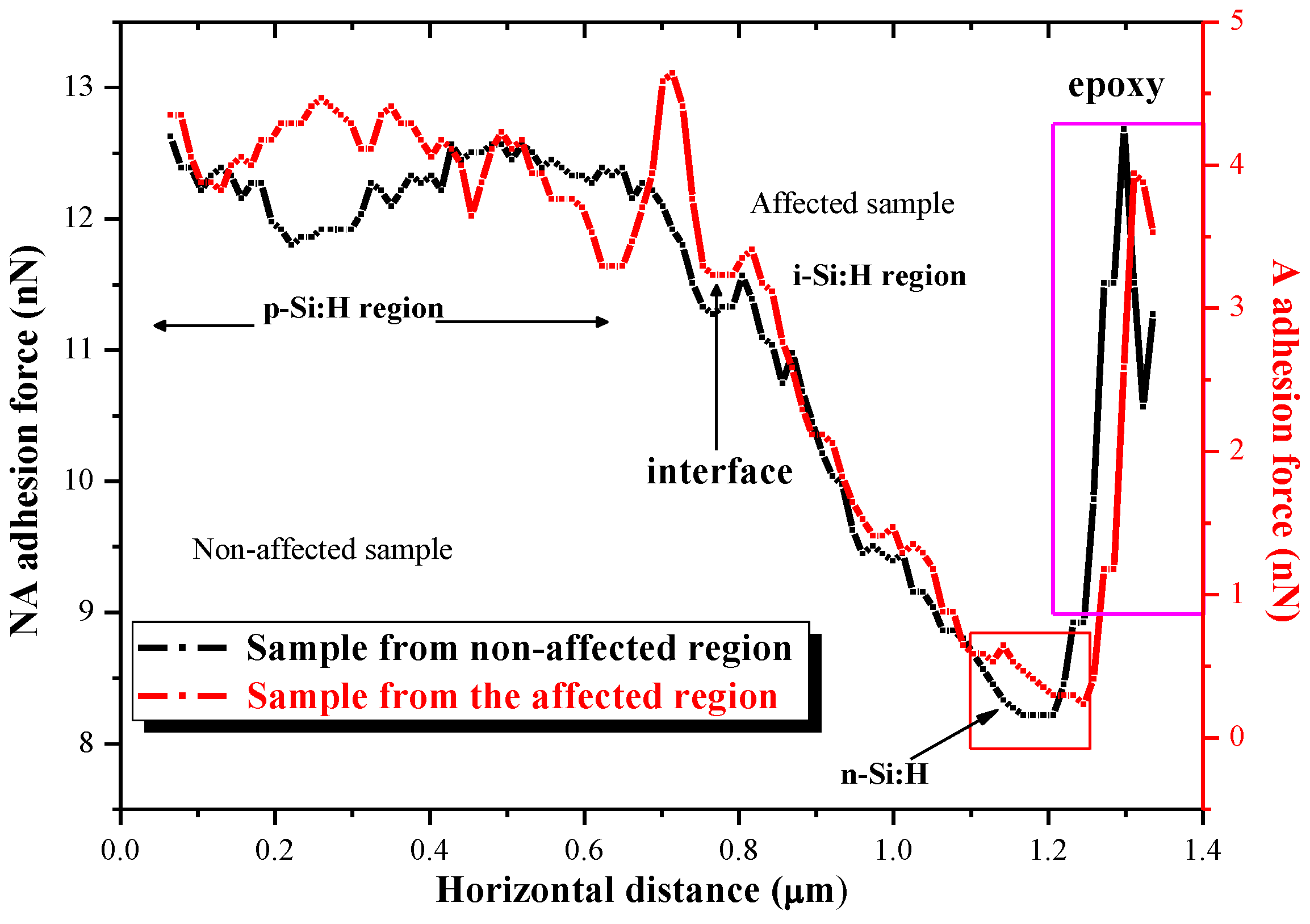
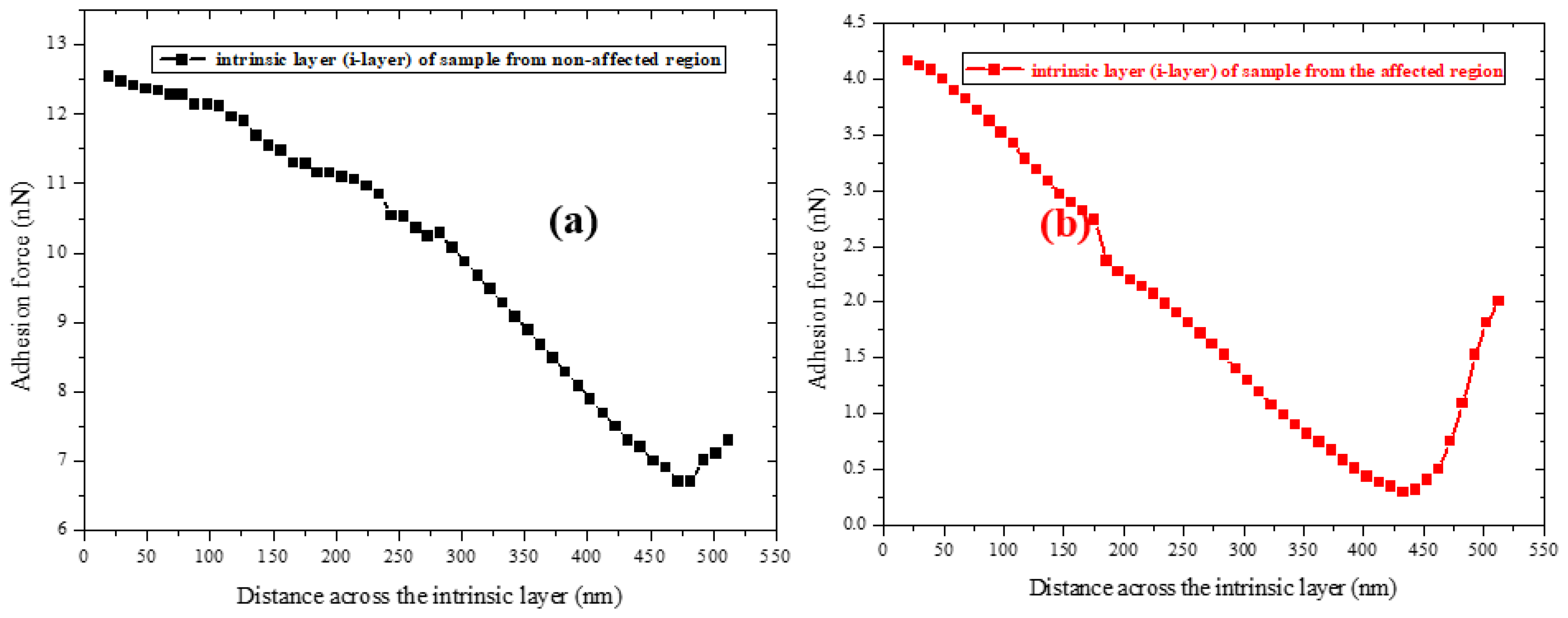
3.1. Adhesion
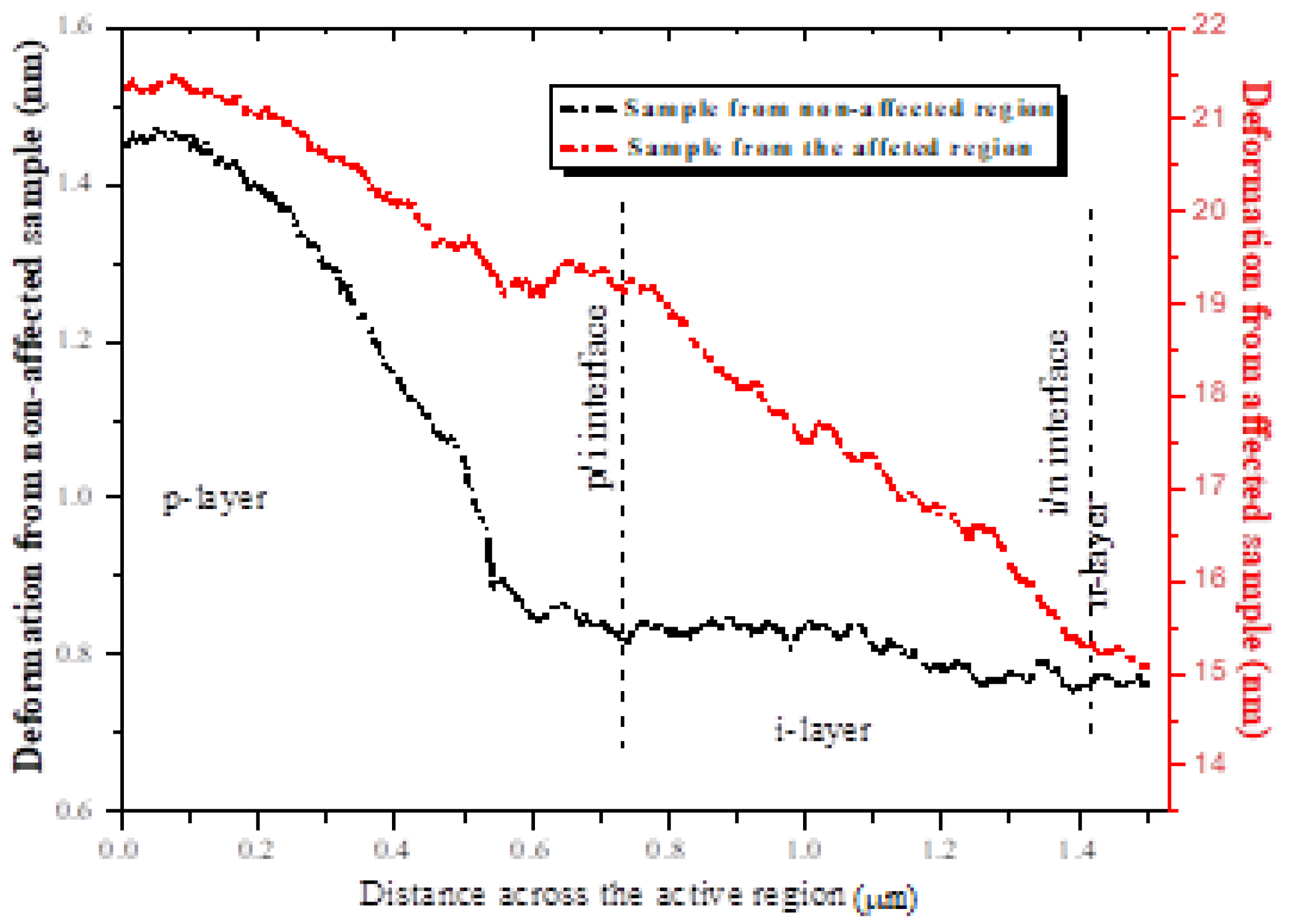
3.2. Deformation
3.3. Deformation and Morphology Analysis
4. Conclusions
Author Contributions
Funding
Acknowledgments
Conflicts of Interest
References
- UN Environment and International Energy Agency. Towards a Zero-Emission, Efficient, and Resilient Buildings and Construction Sector; Global Status Report; UN Environment and International Energy Agency: Paris, France, 2017. [Google Scholar]
- IEA World Energy Outlook 2019. Available online: https://www.iea.org/reports/world-energy-outlook-2019 (accessed on 10 February 2020).
- Almosni, S.; Delamarre, A.; Jehl, Z.; Suchet, D.; Cojocaru, L.; Giteau, M.; Behaghel, B.; Julian, A.; Ibrahim, C.; Tatry, L.; et al. Material challenges for solar cells in the twenty-first century: Directions in emerging technologies. Sci. Technol. Adv. Mater. 2018, 19, 336–369. [Google Scholar] [CrossRef] [PubMed]
- Louwen, A.; van Sark, W.G.J.H.M.; Faaij, A.P.C.; Schropp, R.E.I. Re-assessment of net energy production and greenhouse gas emissions avoidance after 40 years of photovoltaics development. Nat. Commun. 2016, 7, 13728. [Google Scholar] [CrossRef] [PubMed]
- Department of Energy. Photovoltaic System Pricing Trends: Historical, Recent, and Near-Term Projections, 2014th ed.; Department of Energy: Washington, DC, USA, 2014.
- Ogbomo, O.O.; Amalu, E.H.; Ekere, N.N.; Olagbegi, P.O. A review of photovoltaic module technologies for increased performance in tropical climate. Renew. Sustain. Energy Rev. 2017, 75, 1225–1238. [Google Scholar] [CrossRef]
- Paggi, M.; Berardone, I.; Infuso, A.; Corrado, M. Fatigue degradation and electric recovery in silicon solar cells embedded in photovoltaic modules. Sci. Rep. 2014, 4, 4506–4512. [Google Scholar] [CrossRef] [PubMed]
- Paggi, M.; Kajari-Schröder, S.; Eitner, U. Thermomechanical deformations in photovoltaic laminates. J. Strain Anal. Eng. Des. 2011, 46, 772–782. [Google Scholar] [CrossRef]
- Eitner, U. Thermomechanics of Photovoltaic Modules. Ph.D. Thesis, Martin Luther University, Halle-Wittenberg, Germany, 2011. [Google Scholar]
- Koppelaar, R.H.E.M. Solar-PV energy payback and net energy: Meta-assessment of study quality, reproducibility, and results harmonization. Renew. Sustain. Energy Rev. 2017, 72, 1241–1255. [Google Scholar] [CrossRef]
- Knoll, A.; Horvat, A.; Lyakhova, K.S.; Krausch, G.; Sevink, G.J.A.; Zvelindovsky, A.V.; Magerle, R. Phase behavior in thin films of cylinder forming block copolymers. Phys. Rev. Lett. 2002, 89, 035501. [Google Scholar] [CrossRef] [PubMed]
- Sader, J.E.I.; Sanelli, J.A.; Adamson, B.D.; Monty, J.P.; Wei, X.; Crawford, S.A.; Friend, J.R.; Marusic, I.; Mulvaney, P.; Bieske, E.J. Spring constant calibration of atomic force microscope cantilevers of arbitrary shape. Rev. Sci. Instrum. 2012, 83, 103705. [Google Scholar] [CrossRef] [PubMed]
- Shikler, A.; Meoded, T.; Fried, N.; Rosenwaks, Y. Potential imaging of operating light-emitting devices using kelvin force microscopy. Appl. Phys. Lett. 1999, 74, 2972–2974. [Google Scholar] [CrossRef]
- Su, C.; Huang, L.; Neilson, P.; Kelley, V. In-situ measurements of in plane and out-of-plane force gradient with a torsional resonance mode afm. In Proceedings of the 12th International Conference on Scanning Tunnelling Microscopy/Spectroscopy and Related Techniques, Eindhoven, The Netherlands, 30 December 2003; p. 349. [Google Scholar]
- Maboudian, R. Adhesion and friction issues associated with reliable operation of MEMS. Mater. Res. Soc. Bull. 1998, 23, 23–47. [Google Scholar] [CrossRef]
- Osayemwenre, G.O.; Meyer, E.L.; Taziwa, R.T.; Mamphweli, S.N. Photothermal degradation of degraded a-Si:H. Ovonic Res. J. 2017, 10, 421–444. [Google Scholar]
- Mastrangelo, C.H.; Hsu, C.H. A Simple Experimental Technique for the Measurement of the Work of Adhesion of Microstructures; IEEE Solid-State Sensor Actuator Workshop: Hilton Head, SC, USA, 1992; p. 208. [Google Scholar]
- Voigtländer, B. Scanning Probe Microscopy: Atomic Force Microscopy and Scanning Tunneling Microscopy; Springer: Berlin, Germany, 2005; pp. 573–579. [Google Scholar]
- Melitz, W.; Shen, J.; Kummel, A.C.; Lee, S. Surface Science Reports Kelvin probe force microscopy and its application. Surf. Sci. Rep. 2011, 66, 1–27. [Google Scholar] [CrossRef]
- Osayemwenre, G.O.; Meyer, E.L. Confirmation of the degradation of single junction amorphous silicon modules (a-Si:H). Int. J. Photoenergy 2019, 2019, 3452180. [Google Scholar] [CrossRef]
- Barbet, S.; Popoff, M.; Diesinger, H.; Deresmes, D.; Théron, D.; Mélin, T. Cross-talk artefacts in Kelvin probe force microscopy imaging: A comprehensive study. J. Appl. Phys. 2014, 115, 144313. [Google Scholar] [CrossRef]
- Sader, E.J. Calibration of rectangular atomic force microscope cantilevers. Rev. Sci. Instrum. 1999, 70, 3967. [Google Scholar] [CrossRef]
- Osayemwenre, G.O.; Meyer, E.L.; Taziwa, R.T. Investigation of defect in c-Si solar cells by Confocal Raman Spectroscopy. Energy Environ. J. 2018, 29, 1525–1533. [Google Scholar] [CrossRef]
- Sandberg, R.; Boisen, A.; Svendsen, W. Characterization system for resonant micro- and nanocantilevers. Rev. Sci. Instrum. 2005, 76, 125101. [Google Scholar] [CrossRef]


| Sample | Horiz Dist (µm) | Vertical Dist (nm) | Surface Dist (µm) | RmaxRa (nm) | RMS Rq (nm) | Av Height (Ra) (nm) |
|---|---|---|---|---|---|---|
| Affected | 1.243 | −3.265 | 0.265 | 10.091 | 1.455 | 2.895 |
| Non-affected | 1.243 | −0.465 | 0.201 | 5.202 | 0.571 | 1.402 |
| Non-affected (BR) | 1.233 | −0.408 | 0.218 | 6.513 | 0.129 | 1.457 |
© 2020 by the authors. Licensee MDPI, Basel, Switzerland. This article is an open access article distributed under the terms and conditions of the Creative Commons Attribution (CC BY) license (http://creativecommons.org/licenses/by/4.0/).
Share and Cite
Osayemwenre, G.; Meyer, E. Mechanical Degradation Analysis of an Amorphous Silicon Solar Module. Energies 2020, 13, 4126. https://doi.org/10.3390/en13164126
Osayemwenre G, Meyer E. Mechanical Degradation Analysis of an Amorphous Silicon Solar Module. Energies. 2020; 13(16):4126. https://doi.org/10.3390/en13164126
Chicago/Turabian StyleOsayemwenre, Gilbert, and Edson Meyer. 2020. "Mechanical Degradation Analysis of an Amorphous Silicon Solar Module" Energies 13, no. 16: 4126. https://doi.org/10.3390/en13164126
APA StyleOsayemwenre, G., & Meyer, E. (2020). Mechanical Degradation Analysis of an Amorphous Silicon Solar Module. Energies, 13(16), 4126. https://doi.org/10.3390/en13164126