The Design of a Contactless Unregulated Power Converter for the Separated Modules


Abstract
:1. Introduction
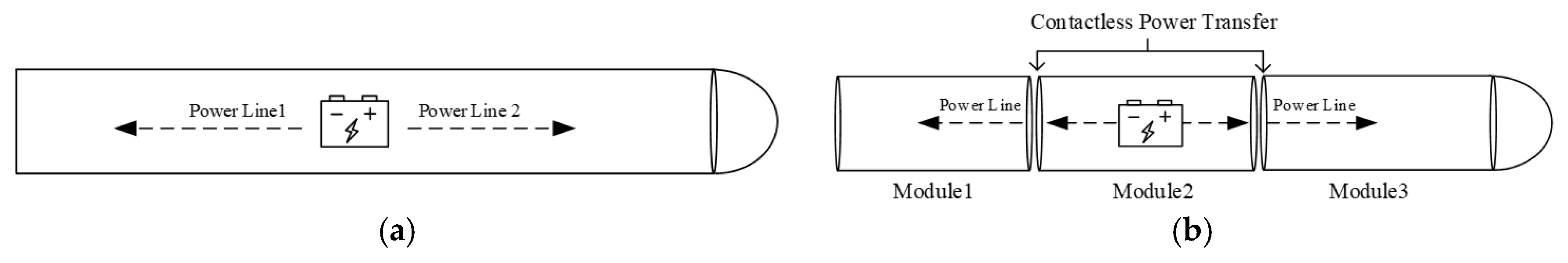
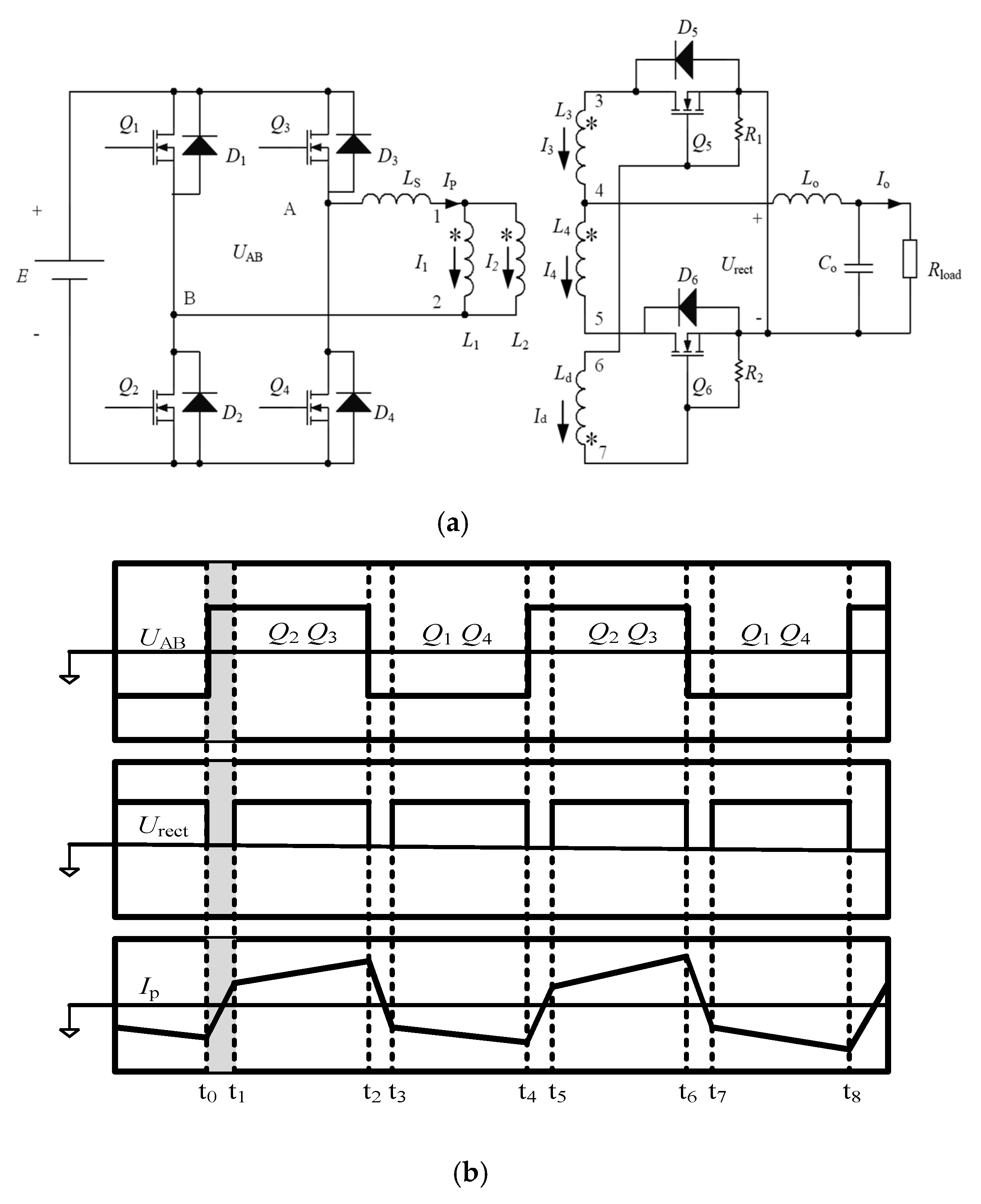
2. System Structure and Equivalent Model
2.1. Operating Principle
2.1.1. Mode I (t0,t1)
2.1.2. Mode II (t1,t2)
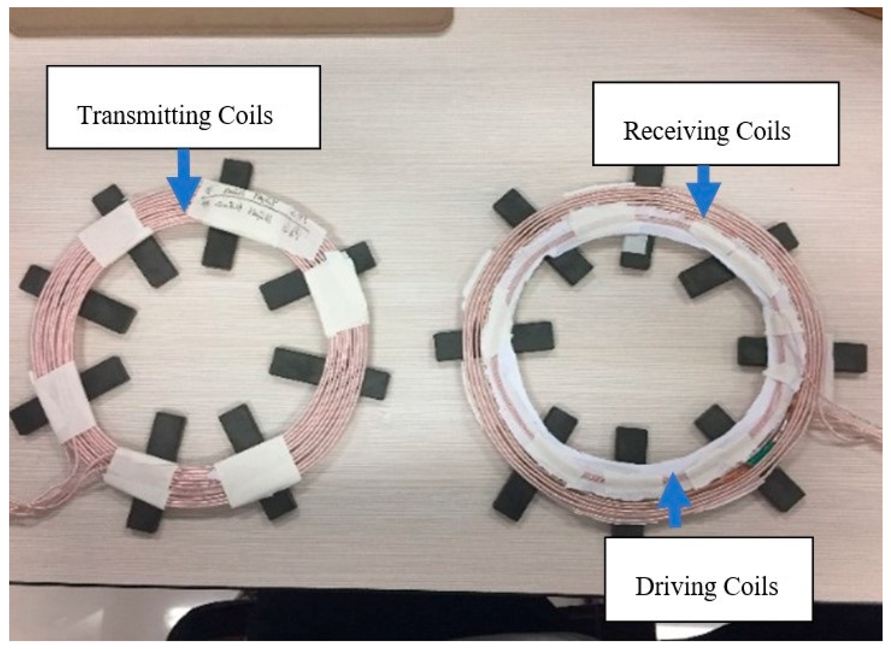
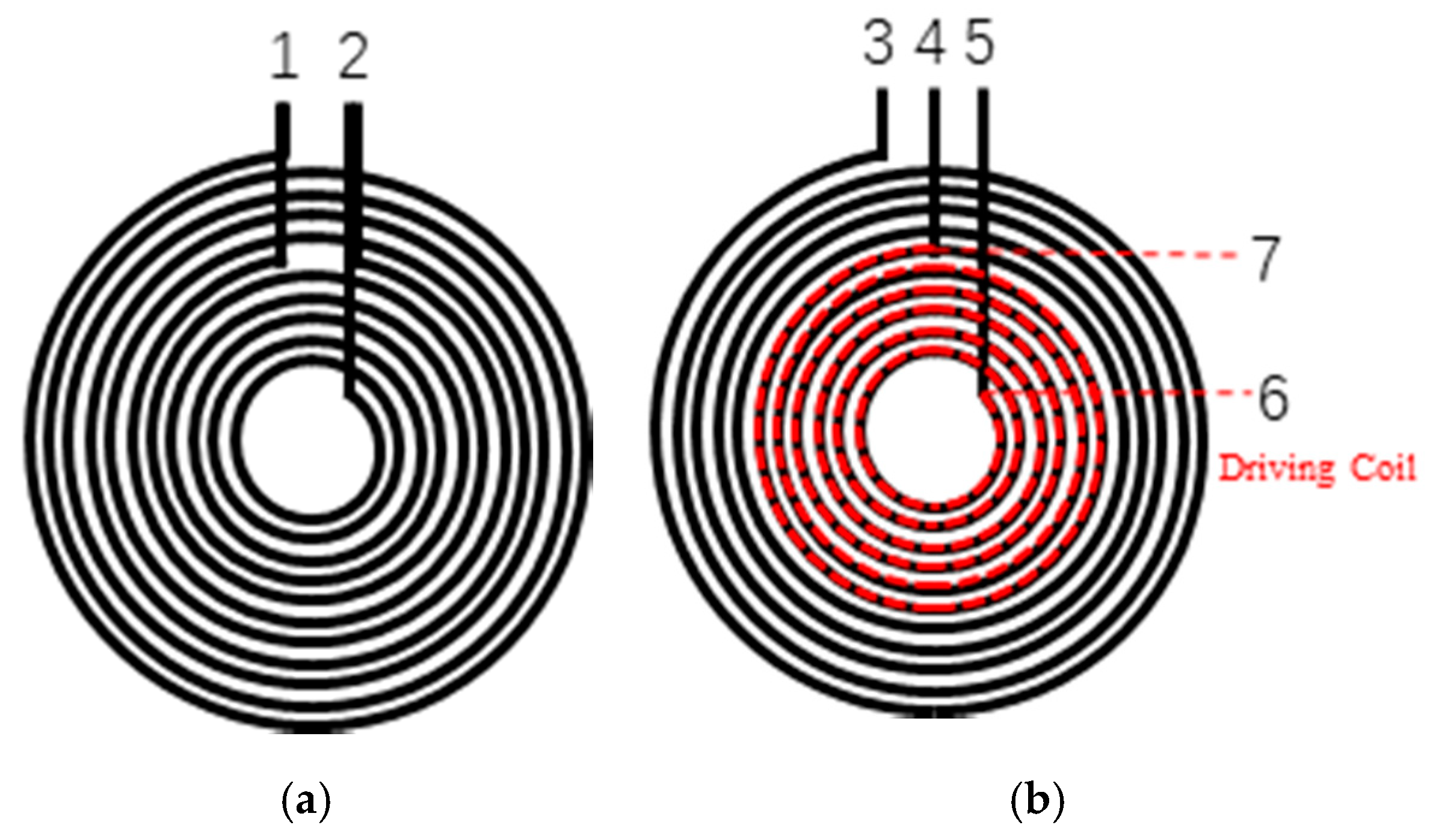
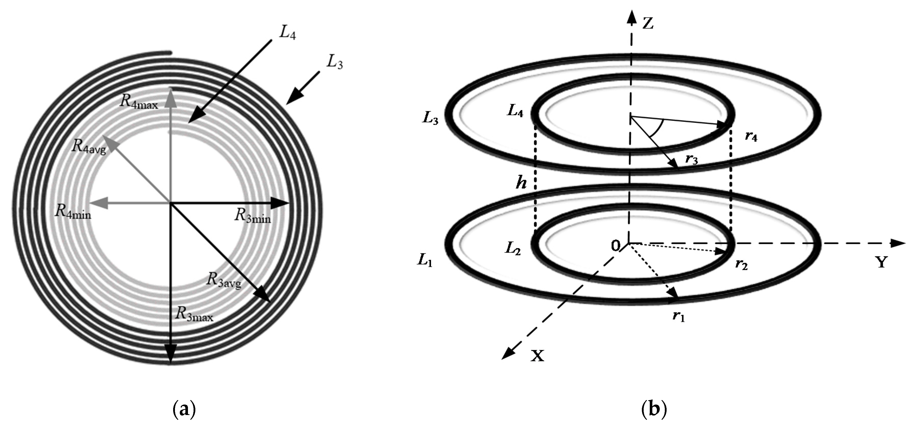
2.2. Coil Structure
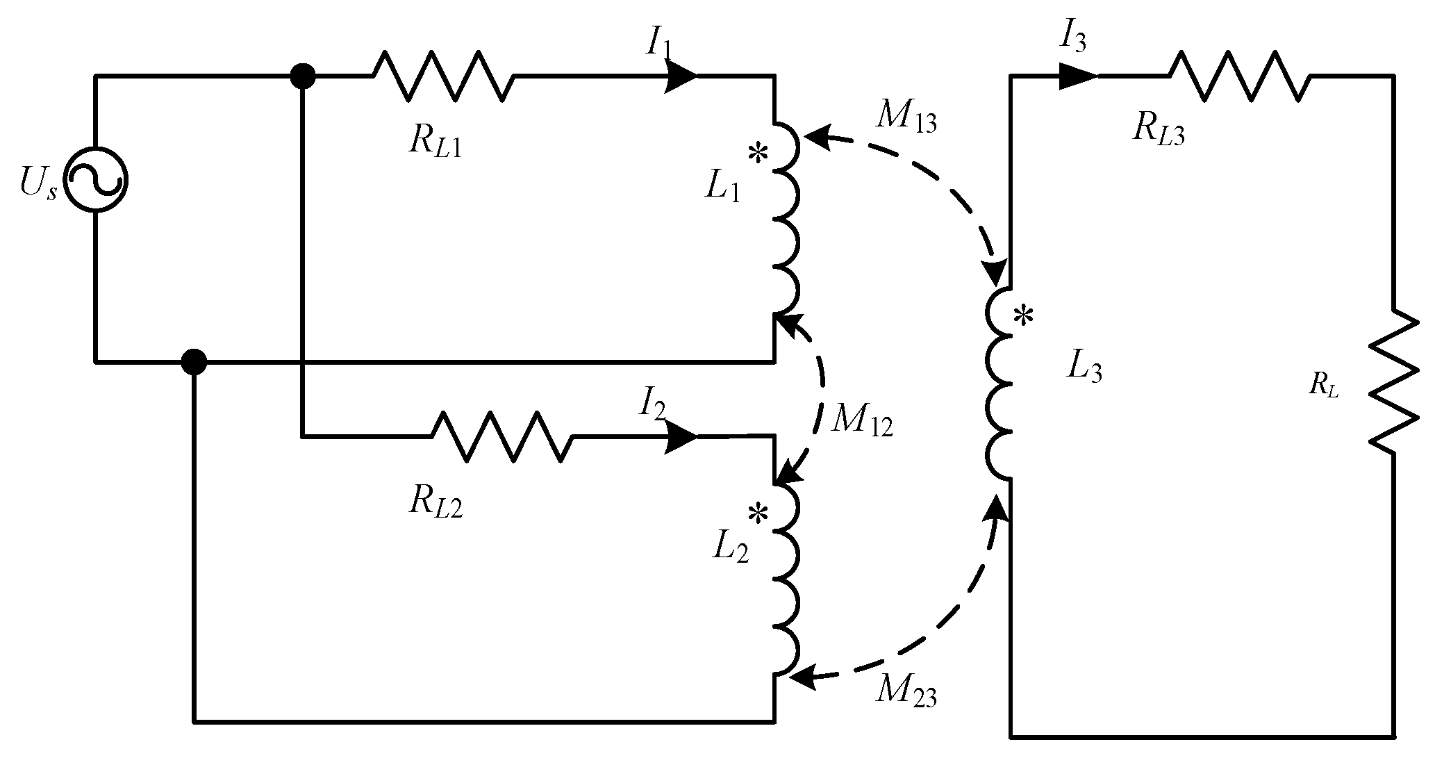
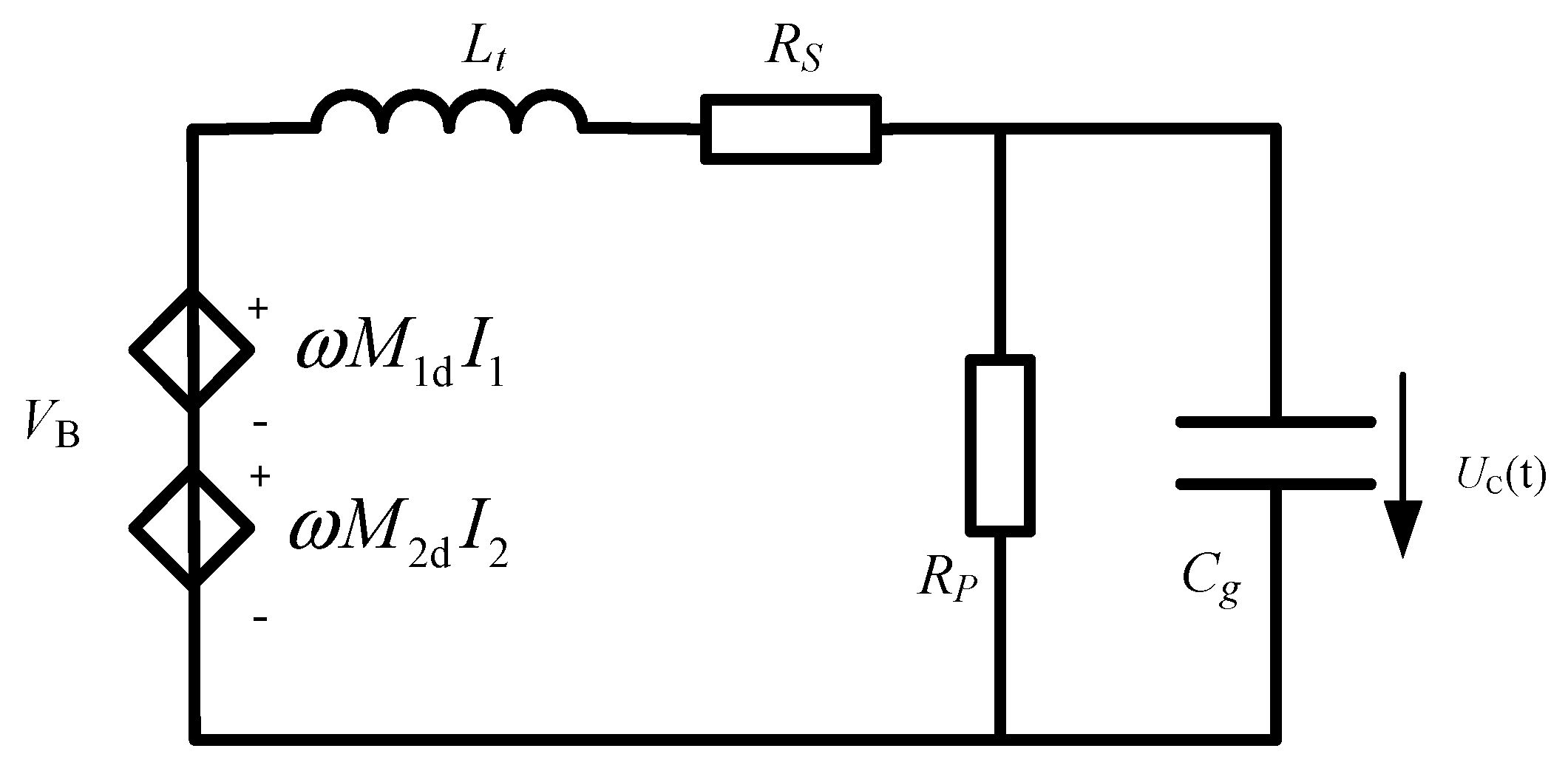
2.3. Equivalent Model
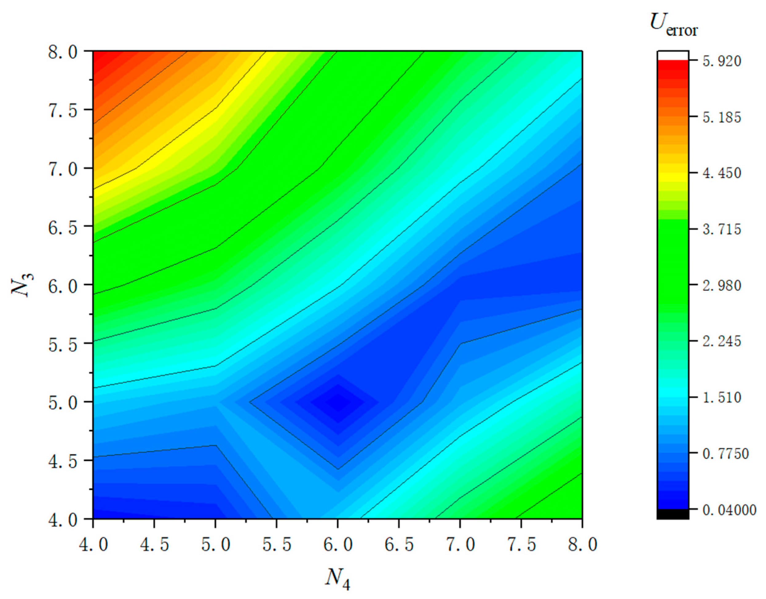
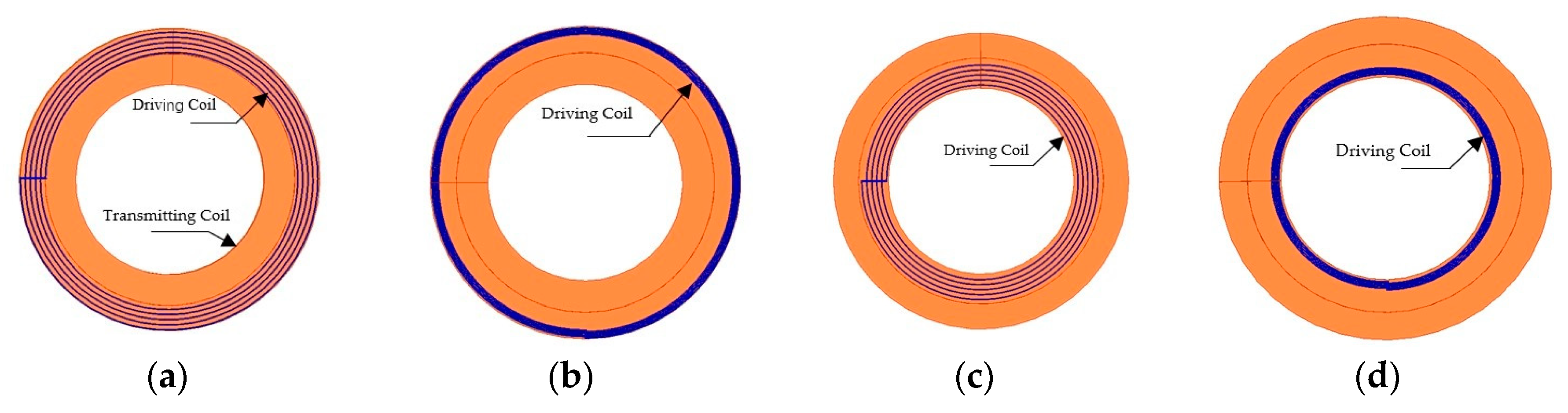
3. Optimal Structure of the Coils
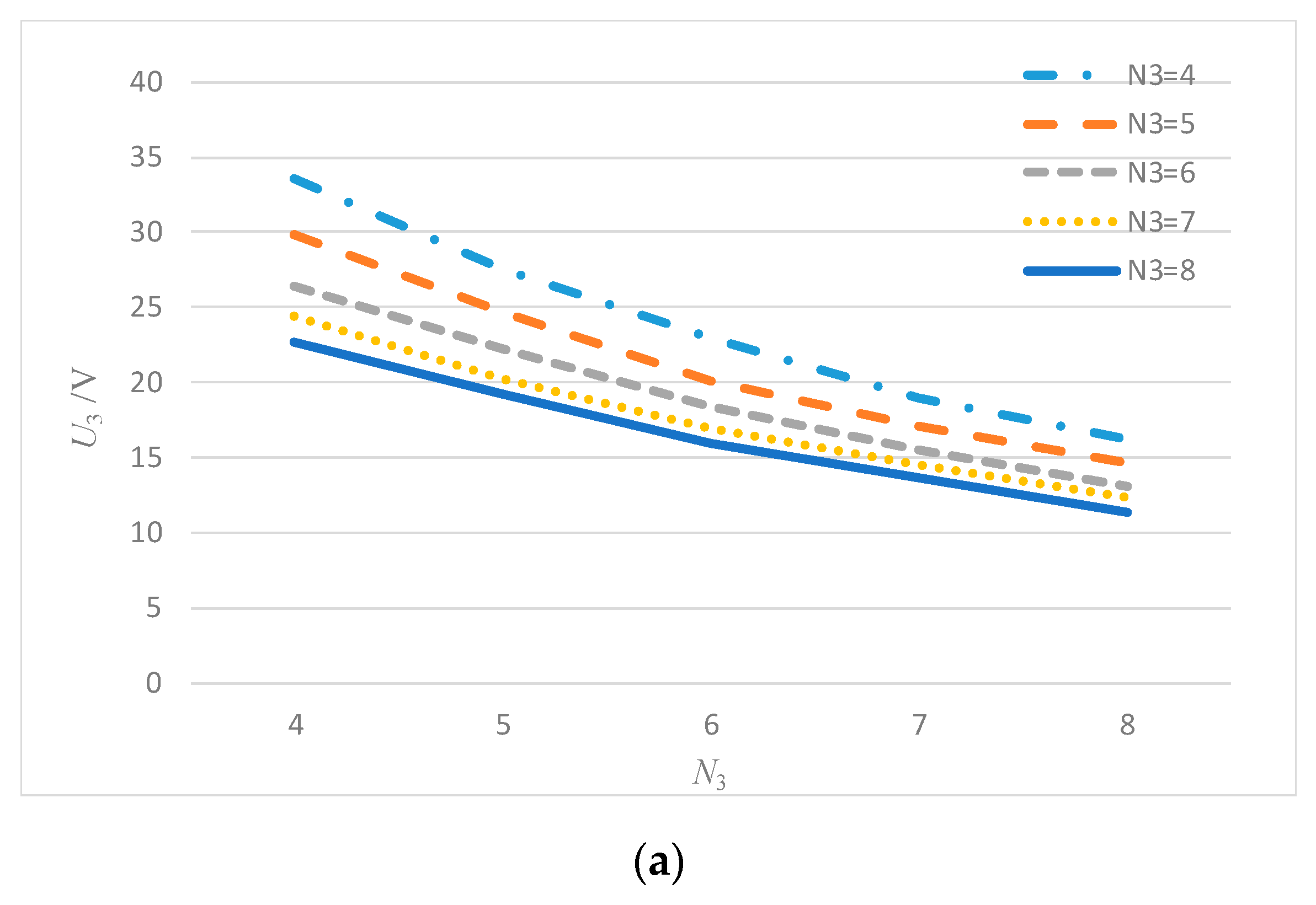
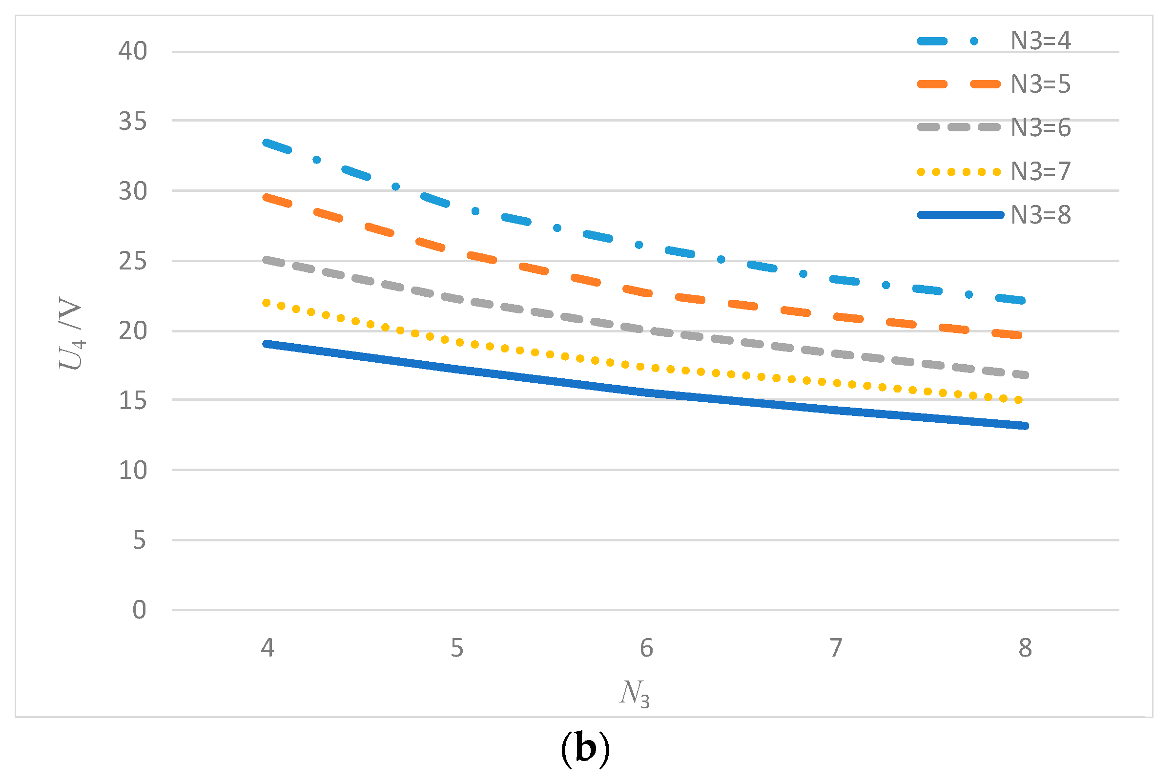
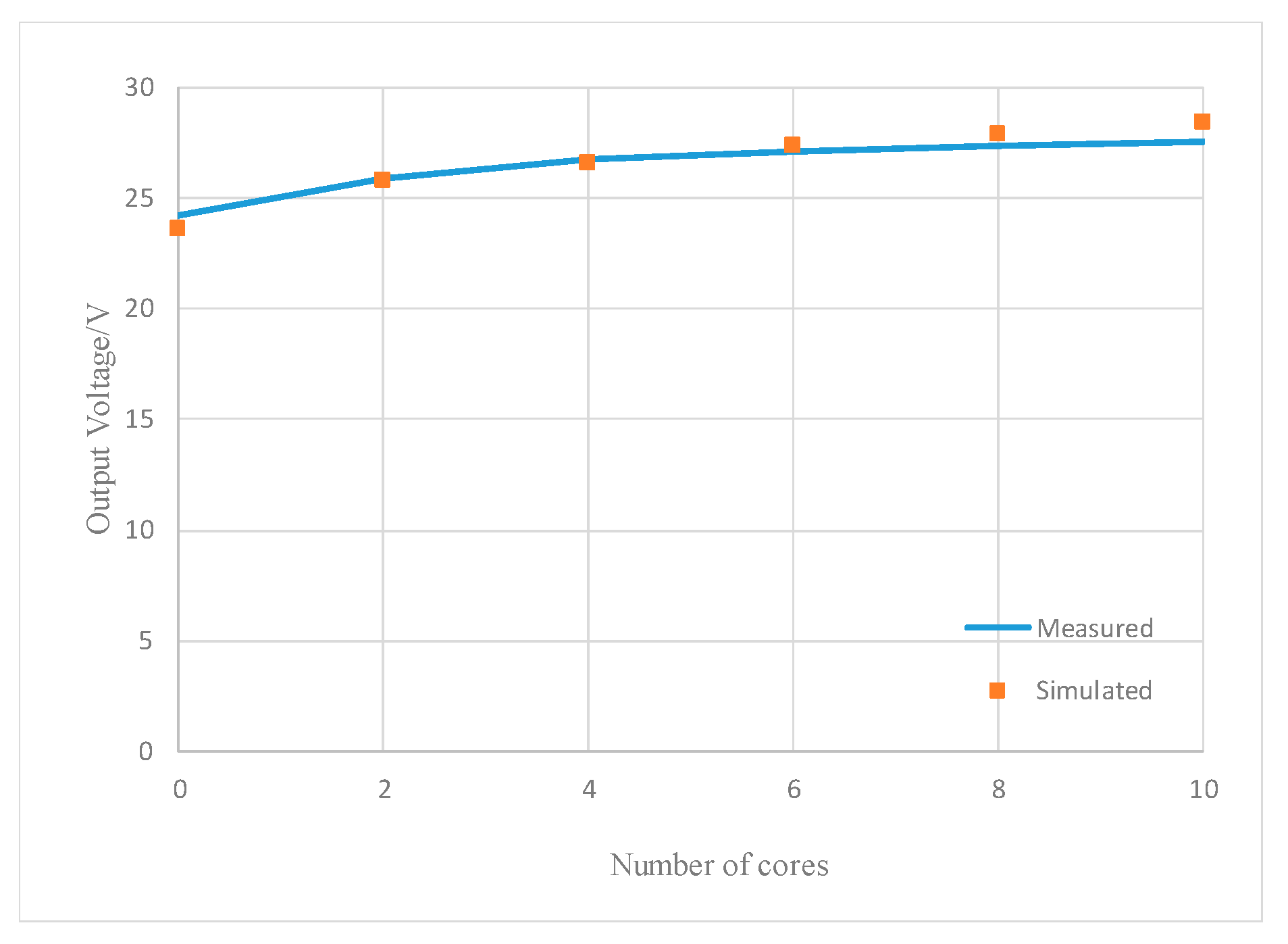
3.1. Relationship between the Induced Voltage and the Number of Turns
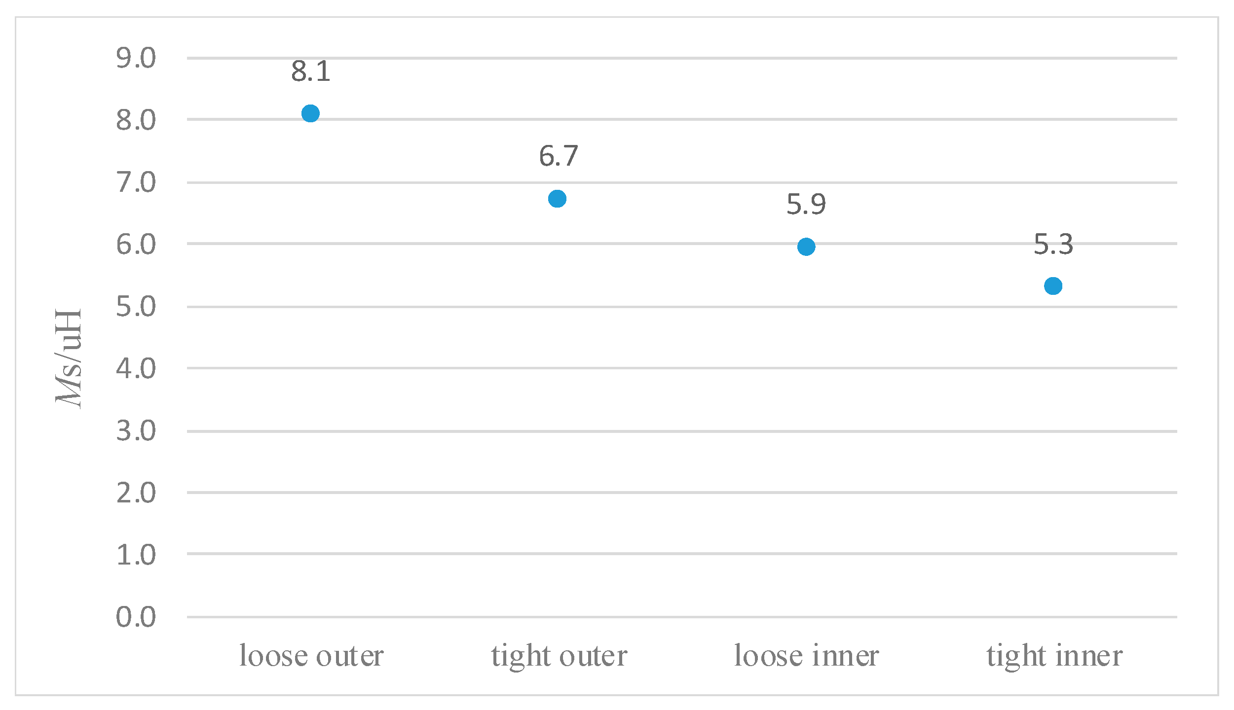
3.2. Driving Coil Arrangement
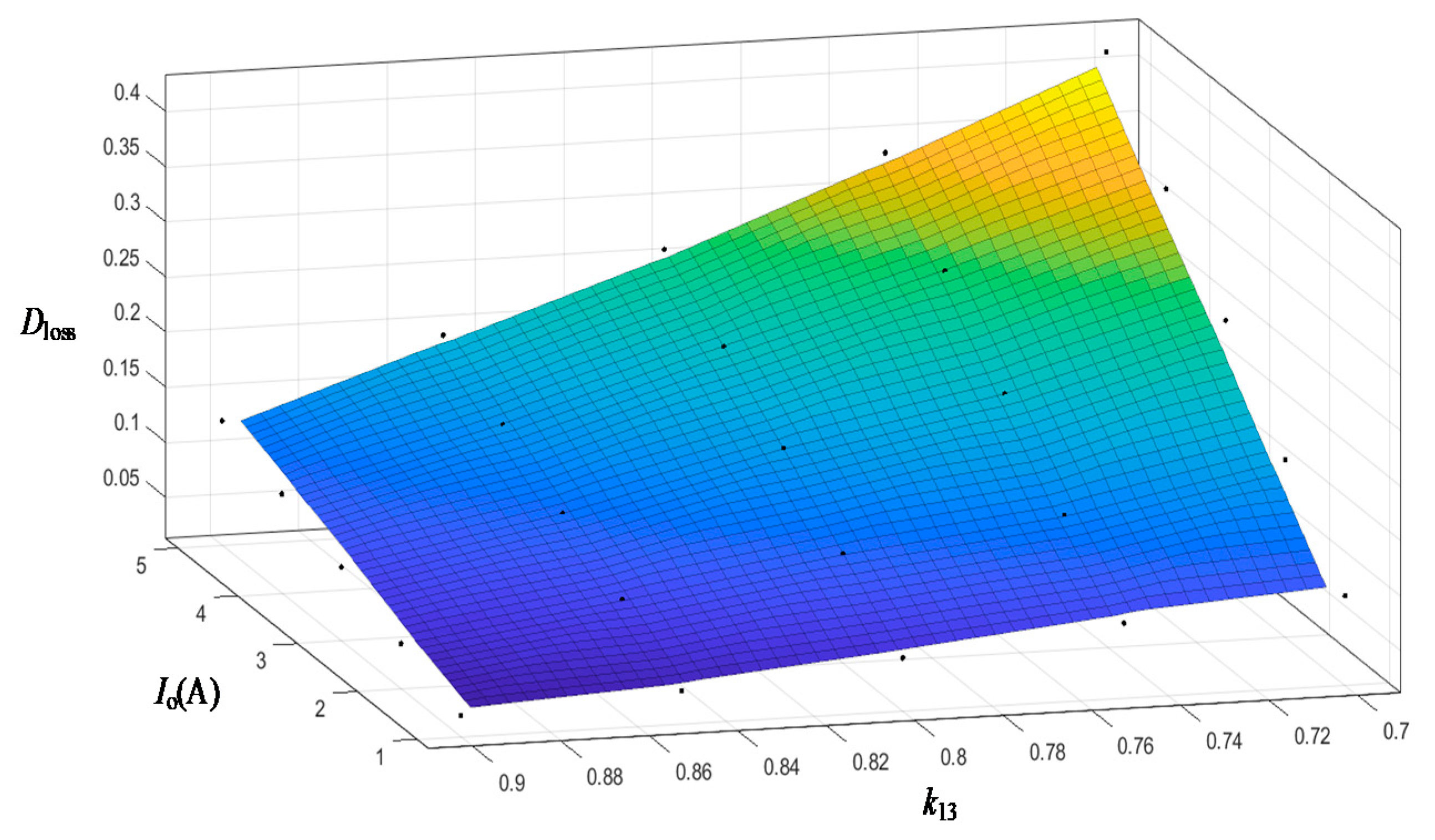
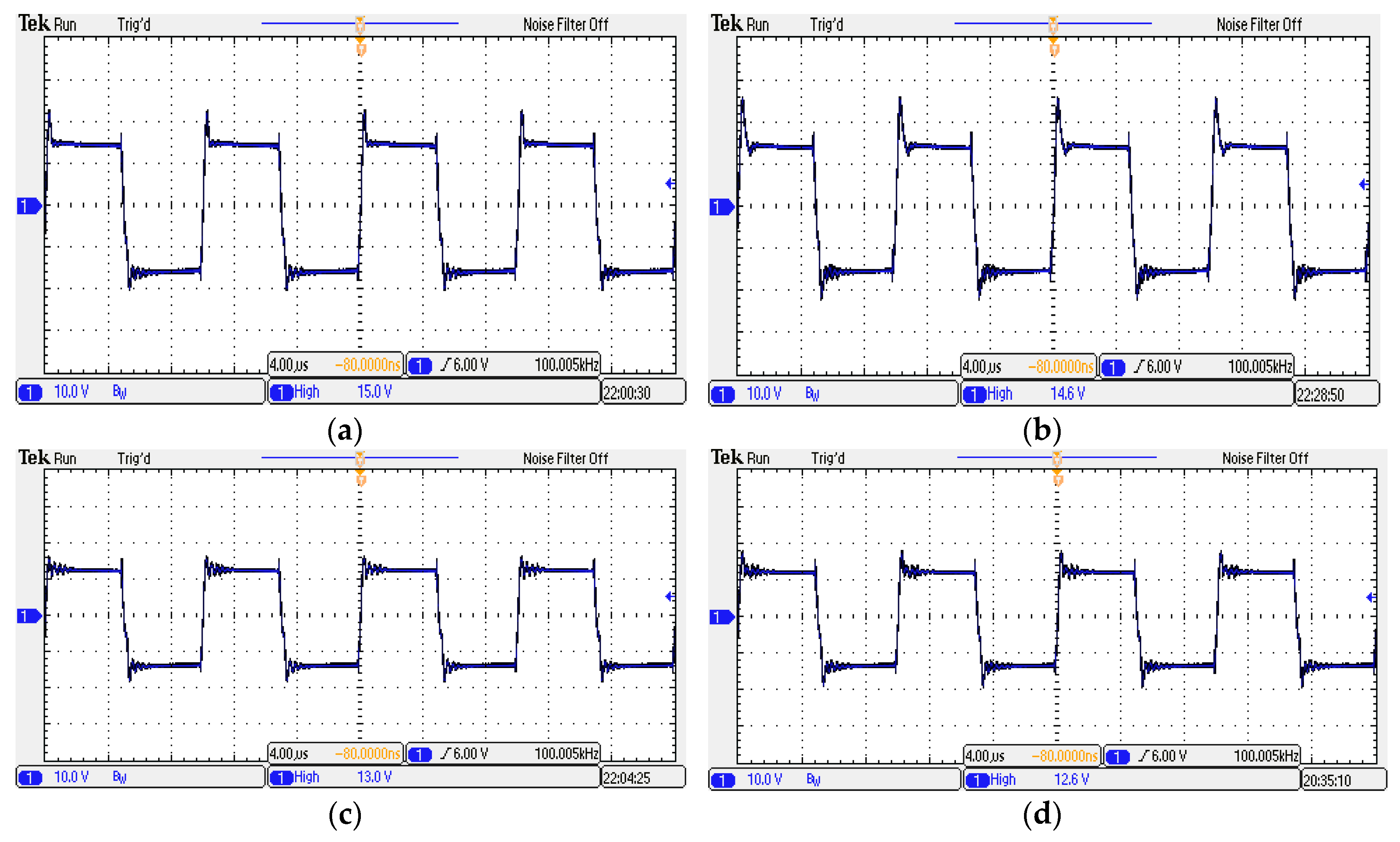
4. Loss of Duty Cycle Analysis
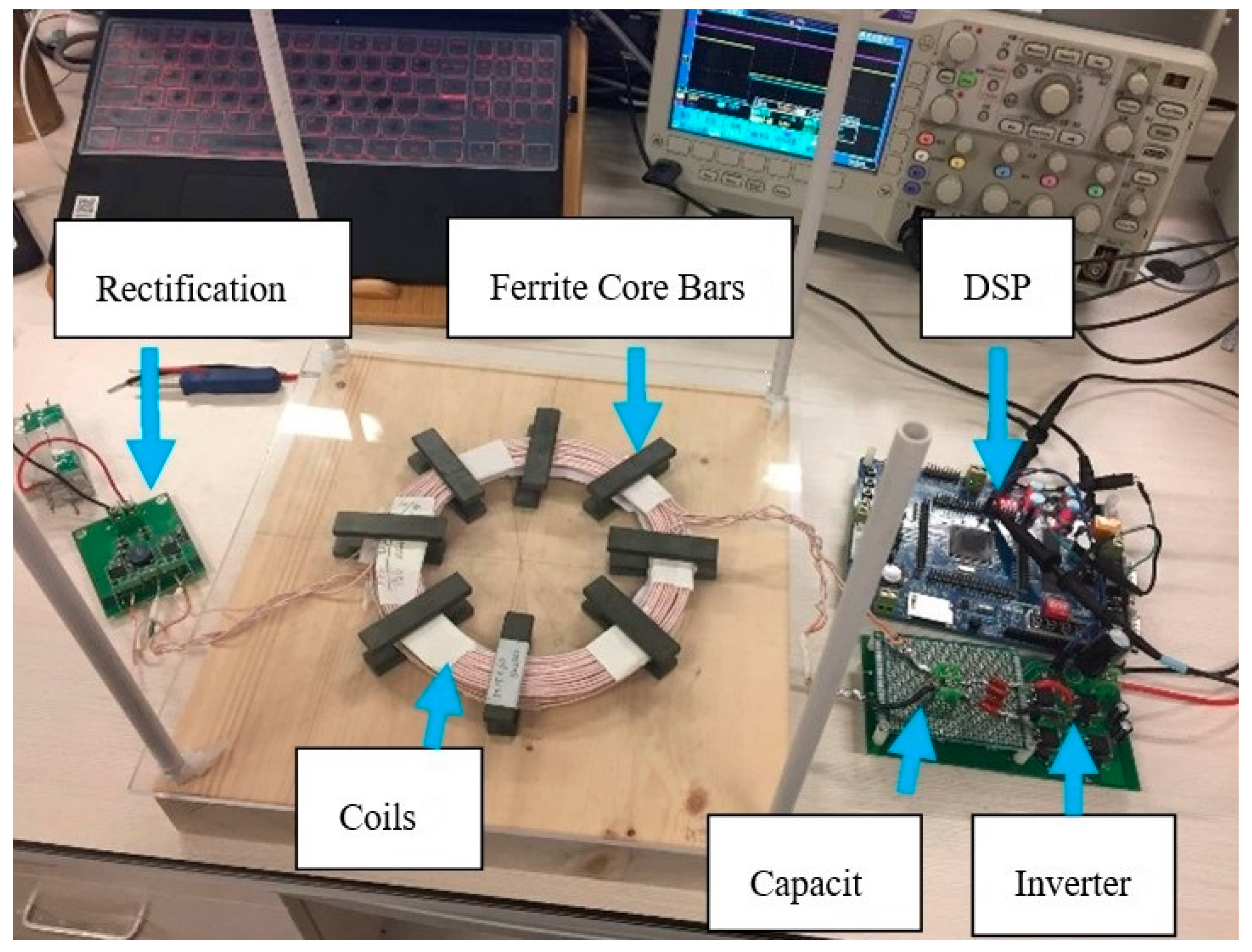
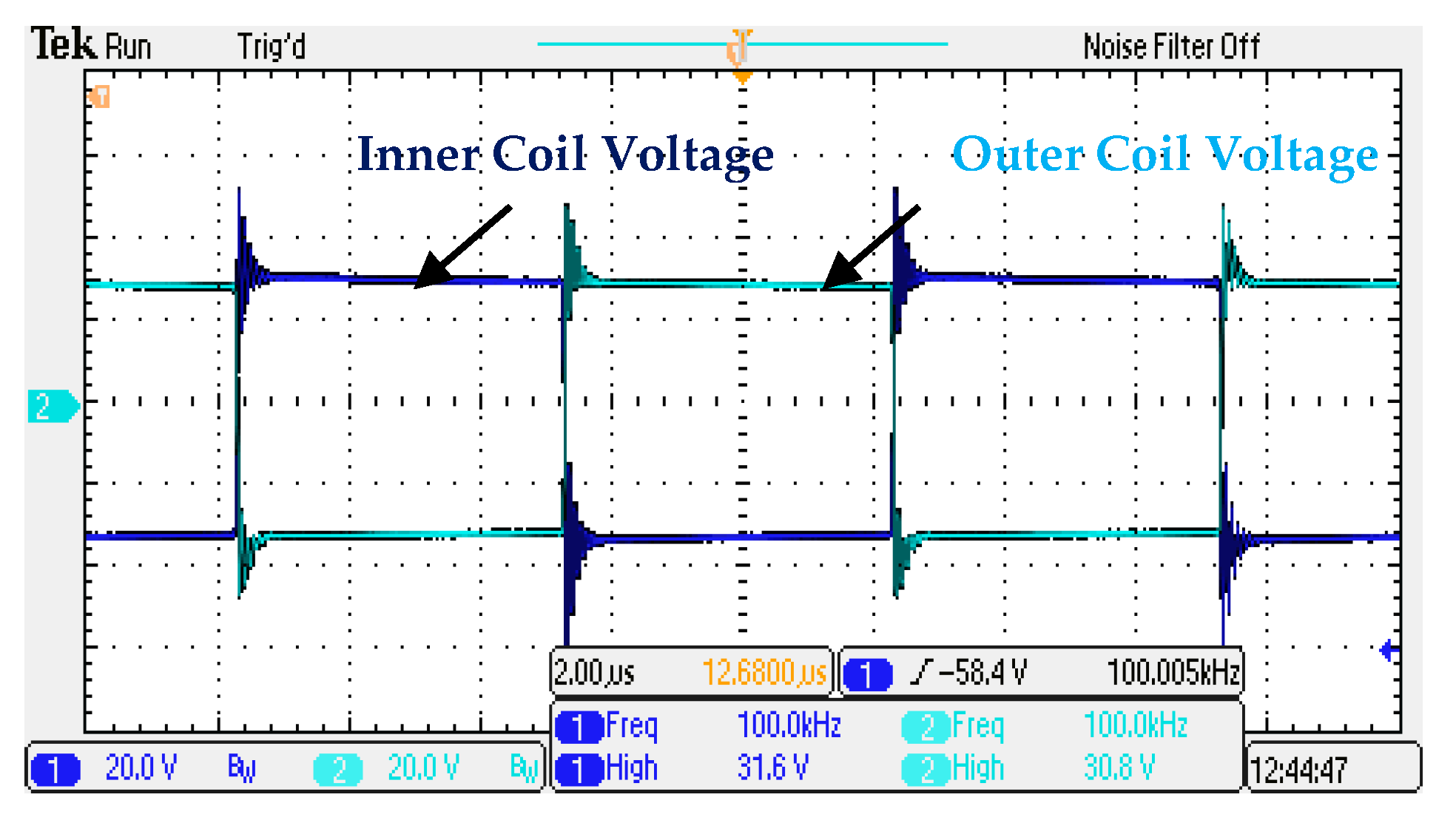
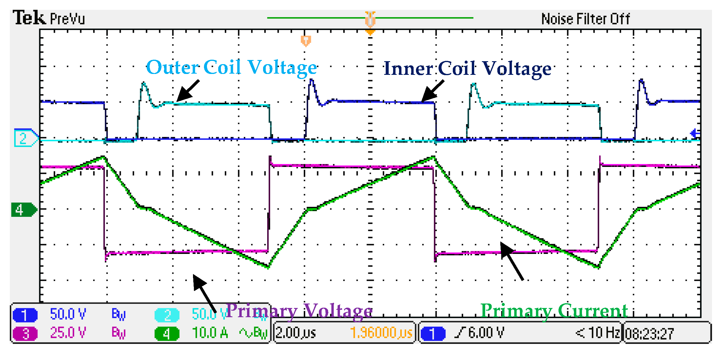
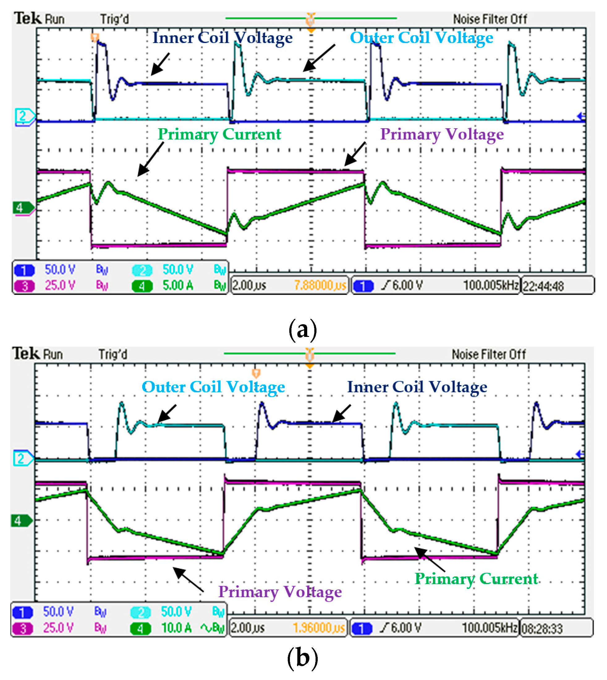
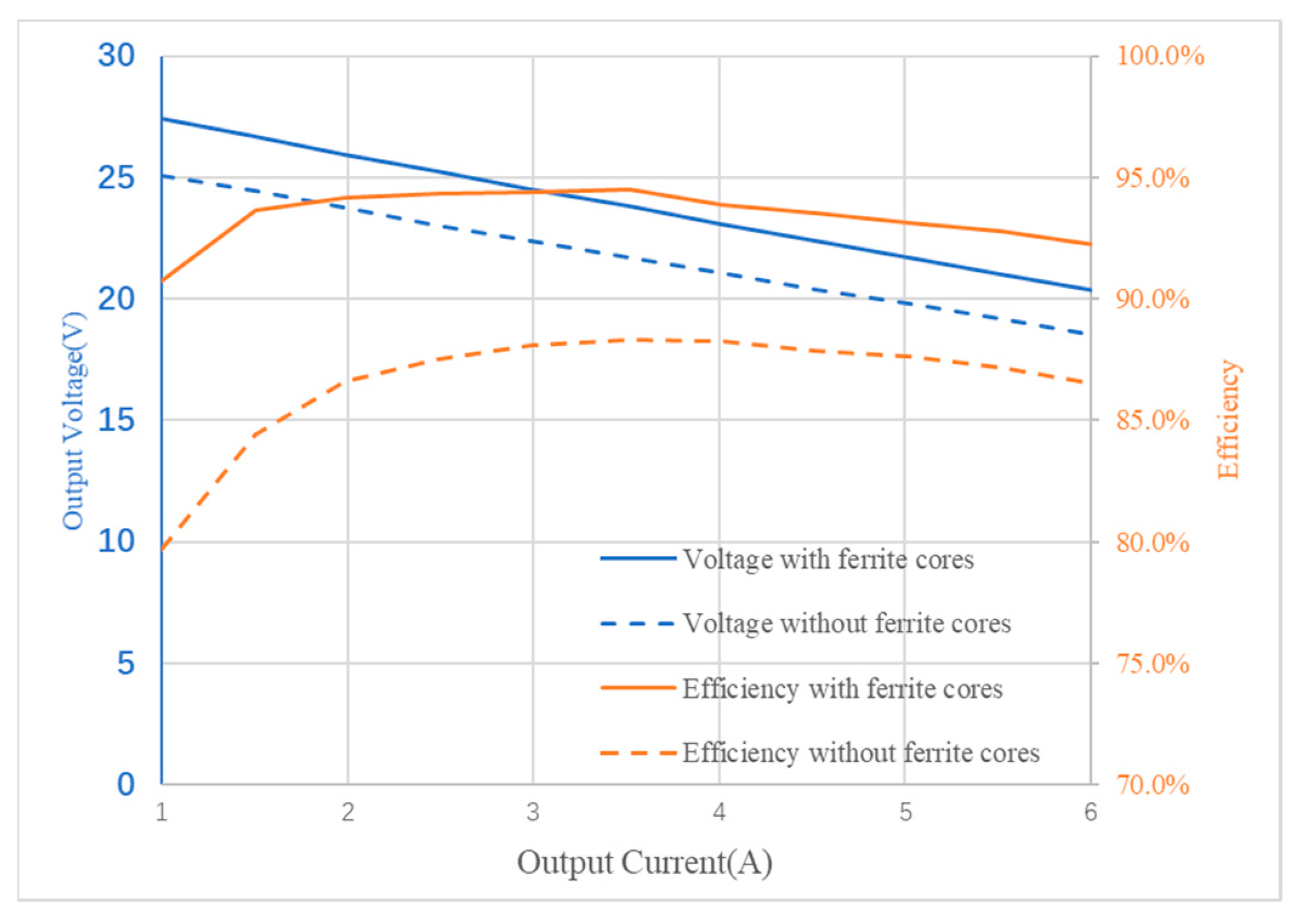
5. Experimental Verification
6. Conclusions
Author Contributions
Funding
Conflicts of Interest
Nomenclature
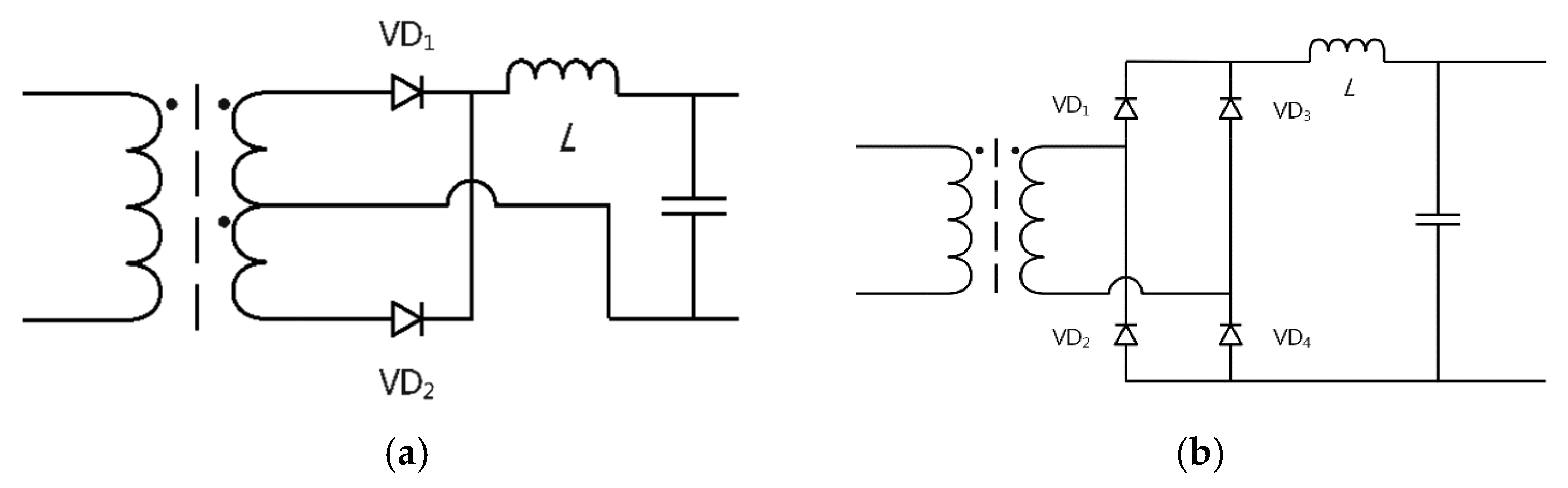
| VD1~VD4 | diodes |
| L1~L4 | power transmitting and receiving coils |
| Ld | driving coil |
| Lo | output filter inductor |
| Ls | leakage inductance on primary side |
| I1~I4 | current in L1,L2,L3,L4,repectively |
| IP | current on leakage inductance |
| Id | current on driving coil |
| D1~D6 | diodes |
| Q1~Q6 | power MOSFET |
| R1,R2 | gate resistance of power MOSFET |
| Rload | Load resistance |
| UAB | Inverter output |
| Urect | rectification voltage |
| Co | output filter capacitor |
| E | DC power supply |
| N1~N4 | turn ratio of coils of L1,L2,L3,L4,respectively |
| M12, M13,M14,M23,M24,M34 | mutual inductance between coils of L1,L2,L3,L4,respectively |
| DSP | Digital Signal Processor |
References
- Thenathayalan, D.; Park, J.H. Wide-Air-Gap transformer model for the design-oriented analysis of contactless power converters. IEEE Trans. Ind. Electron. 2015, 62, 6345–6359. [Google Scholar] [CrossRef]
- Sibué, J.-R.; Kwimang, G.; Ferrieux, J.P.; Meunier, G.; Roudet, J.; Périot, R. A global study of a contactless energy transfer system: Analytical design, virtual prototyping, and experimental validation. IEEE Trans. Power Electron. 2012, 28, 4690–4699. [Google Scholar] [CrossRef]
- Yang, Q.; Lin, B.; Luan, Y.; Duan, J. Distributed capacitance effects on the transmission performance of contactless power transfer for rotary ultrasonic grinding. IET Power Electron. 2018, 11, 548–556. [Google Scholar] [CrossRef]
- Matsumoto, H.; Shibako, Y.; Neba, Y. Contactless power transfer system for AGVs. IEEE Trans. Ind. Electron. 2018, 65, 251–260. [Google Scholar] [CrossRef]
- He, G.; Chen, Q.; Ren, X.; Wong, S.C.; Zhang, Z. Modeling and design of contactless sliprings for rotary applications. IEEE Trans. Ind. Electron. 2019, 66, 4130–4140. [Google Scholar] [CrossRef]
- Covic, G.A.; Boys, J.T. Inductive power transfer. Proc. IEEE. 2013, 101, 1276–1289. [Google Scholar] [CrossRef]
- Covic, G.A.; Boys, J.T. Modern trends in inductive power transfer for transportation applications. IEEE J. Emerg. Sel. Top. Power Electron. 2013, 1, 28–41. [Google Scholar] [CrossRef]
- Low, Z.N.; Chinga, R.A.; Tseng, R.; Lin, J. Design and test of a high-power high-efficiency loosely coupled planar wireless power transfer system. IEEE Trans. Ind. Electron. 2008, 56, 1801–1812. [Google Scholar] [CrossRef]
- Jow, U.-M.; Ghovanloo, M. Geometrical design of a scalable overlapping planar spiral coil array to generate a homogeneous magnetic field. IEEE Trans. Magn. 2013, 49, 2933–2945. [Google Scholar] [CrossRef]
- Miwa, K.; Mori, H.; Kikuma, N.; Hirayama, H.; Sakakibara, K. A consideration of efficiency improvement of transmitting coil array in wireless power transfer with magnetically coupled resonance. In Proceedings of the 2013 IEEE Wireless Power Transfer (WPT), Perugia, Italy, 15–16 May 2013; pp. 13–16. [Google Scholar]
- Santalunai, S.; Thongsopa, C.; Thosdeekoraphat, T. An increasing the power transmission efficiency of flat spiral coils by using ferrite materials for wireless power transfer applications. In Proceedings of the 2014 11th International Conference on Electrical Engineering/Electronics, Computer, Telecommunications and Information Technology (ECTI-CON), Nakhon Ratchasima, Thailand, 14–17 May 2014; pp. 1–4. [Google Scholar]
- Liu, X.; Hui, S.Y. Optimal design of a hybrid winding structure for planar contactless battery charging platform. IEEE Trans. Power Electron. 2008, 23, 455–463. [Google Scholar] [CrossRef]
- Lu, F.; Zhang, H.; Hofmann, H.; Mi, C.C. An inductive and capacitive combined wireless power transfer system with LC-compensated topology. IEEE Trans. Power Electron. 2016, 31, 8471–8482. [Google Scholar] [CrossRef]
- Baek, J.-I.; Kim, C.-E.; Lee, J.-B.; Youn, H.-S.; Moon, G.-W. A simple SR gate driving circuit with reduced gate driving loss for phase-shifted full-bridge converter. IEEE Trans. Power Electron. 2018, 33, 9310–9317. [Google Scholar] [CrossRef]
- TEA1761 Datasheet. Available online: https://www.nxp.com/docs/en/data-sheet/TEA1761T.pdf (accessed on 25 April 2007).
- Fernández, A.; Carbonnier, H.; Mourra, O.; Tonicello, F. 28V bus solar array regulator based on converters with transformer and self-driven Synchronous Rectification. In Proceedings of the 2012 IEEE Energy Conversion Congress and Exposition (ECCE), Raleigh, NC, USA, 15–20 September 2012; pp. 1088–1094. [Google Scholar]
- Qian, T.; Song, W.; Lehman, B. Self-driven synchronous rectification scheme for wide range application of DC/DC converters with symmetrically driven transformers. In Proceedings of the 2006 37th IEEE Power Electronics Specialists Conference, Jeju, Korea, 18–22 June 2006; pp. 1–6. [Google Scholar]
- Zhong, W.X.; Hui, S.Y.; Ho, W.C.; Ho, W.C.; Liu, X. Using self-driven AC–DC synchronous rectifier as a direct replacement for traditional power diode rectifier. IEEE Trans. Ind. Electron. 2012, 59, 392–401. [Google Scholar] [CrossRef]
- Tuomainen, V.; Kyyra, J. Effect of resonant transition on efficiency of forward converter with active clamp and self-driven SRs. IEEE Trans. Power Electron. 2005, 20, 315–323. [Google Scholar] [CrossRef]
- Fernández, A.; Sebastian, J.; Alou, P.; Cobos, J.; Rascon, M. Low output voltage AC/DC converter with a new scheme of synchronous rectification that complies with IEC 1000-3-2 regulations. IEEE Trans. Power Electron. 2003, 18, 966–974. [Google Scholar] [CrossRef]
- Gu, Y.; Lu, Z.; Qian, Z.; Huang, G. A novel driving scheme for synchronous rectifier suitable for modules in parallel. IEEE Trans. Power Electron. 2005, 20, 1287–1293. [Google Scholar] [CrossRef]
- Guan, Y.; Wang, Y.; Bian, Q.; Hu, X.; Wang, W.; Xu, D. High-efficiency self-driven circuit with parallel branch for high frequency converters. IEEE Trans. Power Electron. 2018, 33, 926–931. [Google Scholar] [CrossRef]
- Qian, T.; Song, W.; Lehman, B. Self-driven synchronous rectification scheme without undesired gate-voltage discharge for DC-DC converters with symmetrically driven transformers. IEEE Trans. Power Electron. 2008, 23, 506–510. [Google Scholar] [CrossRef]
- Dill, H.G. Designing inductors for thin-film applications. Electron. Des. 1964, 17, 52–60. [Google Scholar]
- Maxwell, J.C. A Treatise on Electricity and Magnetism; Dover: New York, NY, USA, 1954. [Google Scholar]
- Alou, P.; Cobos, J.; Garcia, O.; Prieto, R.; Uceda, J. A new driving scheme for synchronous rectifiers: Single winding self-driven synchronous rectification. IEEE Trans. Power Electron. 2001, 16, 803–811. [Google Scholar] [CrossRef]
- Wang, H.; Chung, H.S.-H.; Ioinovici, A. A class of high-input low-output voltage single-step converters with low voltage stress on the primary-side switches and high output current capacity. IEEE Trans. Power Electron. 2011, 26, 1659–1672. [Google Scholar] [CrossRef]


| Parameters | Value |
|---|---|
| L1, L3/uH | 21.8(N1 = 5) |
| L2, L4/uH | 22.5(N2 = 6) |
| Air gap distance/mm | 2 |
| Coil diameter /mm | 75 |
| Input Voltages Us/V | 30 |
| Frequency f/kHz | 100 |
| Ferrite core bars | PC40 (5 × 15 × 60 mm) |
| Litz wire | 300 strands × 0.1 mm |
© 2020 by the authors. Licensee MDPI, Basel, Switzerland. This article is an open access article distributed under the terms and conditions of the Creative Commons Attribution (CC BY) license (http://creativecommons.org/licenses/by/4.0/).
Share and Cite
Zhou, Y.; Sun, Y.; Yang, Z. The Design of a Contactless Unregulated Power Converter for the Separated Modules. Energies 2020, 13, 4118. https://doi.org/10.3390/en13164118
Zhou Y, Sun Y, Yang Z. The Design of a Contactless Unregulated Power Converter for the Separated Modules. Energies. 2020; 13(16):4118. https://doi.org/10.3390/en13164118
Chicago/Turabian StyleZhou, Yan, Yu Sun, and Ziwen Yang. 2020. "The Design of a Contactless Unregulated Power Converter for the Separated Modules" Energies 13, no. 16: 4118. https://doi.org/10.3390/en13164118
APA StyleZhou, Y., Sun, Y., & Yang, Z. (2020). The Design of a Contactless Unregulated Power Converter for the Separated Modules. Energies, 13(16), 4118. https://doi.org/10.3390/en13164118