Electro-Thermal Simulation of Vertical VO2 Thermal-Electronic Circuit Elements


Department of Electron Devices, Budapest University of Technology and Economics, 1117 Budapest, Hungary
*
Author to whom correspondence should be addressed.
Energies 2020, 13(13), 3447; https://doi.org/10.3390/en13133447
Submission received: 15 May 2020
/
Revised: 26 June 2020
/
Accepted: 1 July 2020
/
Published: 3 July 2020
(This article belongs to the Special Issue Thermal and Electro-thermal System Simulation 2020)
Abstract
:Advancement of classical silicon-based circuit technology is approaching maturity and saturation. The worldwide research is now focusing wide range of potential technologies for the “More than Moore” era. One of these technologies is thermal-electronic logic circuits based on the semiconductor-to-metal phase transition of vanadium dioxide, a possible future logic circuits to replace the conventional circuits. In thermal-electronic circuits, information flows in a combination of thermal and electronic signals. Design of these circuits will be possible once appropriate device models become available. Characteristics of vanadium dioxide are under research by preparing structures in laboratory and their validation by simulation models. Modeling and simulation of these devices is challenging due to several nonlinearities, discussed in this article. Introduction of custom finite volumes method simulator has however improved handling of special properties of vanadium dioxide. This paper presents modeling and electro-thermal simulation of vertically structured devices of different dimensions, 10 nm to 300 nm layer thicknesses and 200 nm to 30 μm radii. Results of this research will facilitate determination of sample sizes in the next phase of device modeling.
1. Introduction
Miniaturization of electronic devices’ feature size is the primary driver of computing development. Scaling down has been described by Moore’s law for many years. Recently, complimentary metal–oxide–semiconductor (CMOS) scaling down has been slower than ever before owing to scaling limits that appear on very small dimensions. The technological advancement described by Moore’s Law for CMOS technology since the past 50 years is expected to flatten out completely by 2025 [1,2]. Finding “Beyond CMOS” solutions has become more essential to keep the computing advancement flourishing. It takes about 10 years for a new technology to move from the laboratory to mass production, for example, FinFET [1]. There are several potential “More than Moore” devices in laboratories [3], but currently, none is in a phase to state that this will be the successor.
A report commissioned by the Defense Technical Information Center (DTIC) [4] proposes four basic computational models: classical digital computing, analog computing, neuro-inspired computing and quantum computing. The latter three areas are suitable for solving special problems much more effectively than before; however, they are generally not able to replace traditional tasks where classical digital computing performs well, such as 3D graphics, mobile devices and similar others.
Architecture specialization can help to increase computing power for a while [5], for example, the use of tensor processing units (TPUs) developed for artificial intelligence (AI) [6] or the wider use of field-programmable gate arrays (FPGAs) in data centers [7]. The degree of specialization is well illustrated by the fact that there were 4 separate accelerators in the Apple A4 system on a chip (SoC), 28 in the A8, and more than 40 in the A12 [8]. Another way to increase the performance of CMOS technology-based systems is to use design and technological developments such as chip stacking in 3D using through-silicon vias (TSVs) [9], advanced energy management, near-threshold voltage (NTV) operation and application of an increased number of metal layers [3].
Following are some more promising future devices compatible with CMOS technology [10]:
- In a tunneling FET, conduction occurs through band-to-band tunneling. Gate voltage shifts the energy bands and changes the probabilities of tunneling [11].
- In a graphene pn-junction, transmission or a total internal reflection of electrons occurs by switching the electrostatic p and n doping of graphene by applying voltage to electrodes. The current routes to one or other output of the device [12].
- The bilayer pseudospin FET is an orbitronic device. Holes are injected into one monolayer of graphene and electrons into another monolayer and they may bind into excitons. The excitons may relax into a Bose–Einstein condensate (BEC) state. The current between source and drain first grows with the increase of voltage and then decreases as the carrier imbalance destroys BEC causing negative differential resistance [13].
- Spintronic devices are based on magnetic dipoles represented by electrons with polarized spins or ferromagnetic elements. Spintronic devices are nonvolatile (preserve the state when the power is turned off). Some possible types are as follows: The SpinFET combines a MOSFET and a switchable magnetic element [14]. The spin transfer domain wall device operates by the motion of a domain wall in a ferromagnetic wire [15]. The spintronic majority gate uses ferromagnetic wires and majority of the input currents’ directions sets the direction of magnetization [16]. In the all spin logic device, nanomagnets are placed over a copper wire and a diffusion spin current exerts a torque on a nanomagnet to switch its polarization [17].
In this article, we discuss a potential device that is compatible with CMOS integration and in which information transmits by two physical processes: electrical and thermal. This device is the phonsistor (a portmanteau of “phonon transistor”) [18]. A digital circuit can be built from this device, which is called thermal-electronic logic circuits (TELC) [19,20]. TELC can be implemented using materials that have semiconductor-to-metal transition (SMT). Vanadium dioxide (VO2) has shown properties as a good candidate for implementation of TELC structures with its SMT at around 67 °C [21].
Vanadium dioxide has some special properties whose investigation is not yet complete. Its optical properties [22], the relationship between SMT and structural phase transition [23,24], the nature of SMT [20,25] or the monoclinic metallic phase [26] are studied. Its applications cover many areas such as thermal rectification [27,28], high performance electromechanical switches [29], smart window coatings [30], neuromorphic devices [31,32] and non-volatile memory arrays [32]. Phonsistor and TELC are not the only transistor-type applications, we also find examples of purely thermal transistors in the literature [33,34].
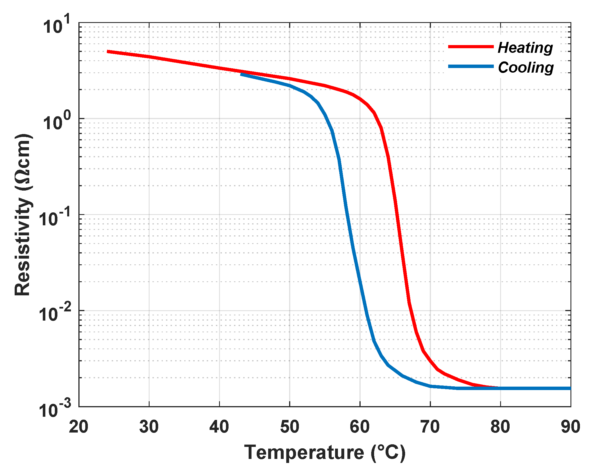
VO2 encounters electrical resistivity change when it exposes to heat. The material shows much lesser ability to conduct electrical current at room temperature than at higher temperatures. Moreover, the resistivity drops steeply around 67 °C (340 K), changing the material electrical properties to a conductor. The transition from a low-conducting phase to a high-conducting phase is called “semiconductor-to-metal transition” (SMT). Phase transition occurs due to the sudden change in the structure of VO2 from the tetragonal structure (at low temperatures) to the monoclinic structure (at high temperatures) [19]. Figure 1 illustrates the electric resistivity change by 3 to 4 orders of magnitude versus temperature. The electro-thermal behavior of VO2 is highly technology-dependent. It also depends on the manufacturing process and the substrate [35,36,37].
A simple phonsistor consists of two components: a heating resistor and an SMT resistor. The heat generated by Joule heating in the resistor transports by phonons to the SMT resistor by diffusion. This process is similar to the diffusion of minority charge carriers at the base of a bipolar transistor. The switching voltage and holding current of the SMT resistor decrease due to external heating; this is the role of the heating resistor [38]. The abrupt variation in the VO2 electric resistivity makes it capable of switching on and off electrically depending on its thermal state. Hence the term “thermal-electronic logic circuits” (TELC) is used.
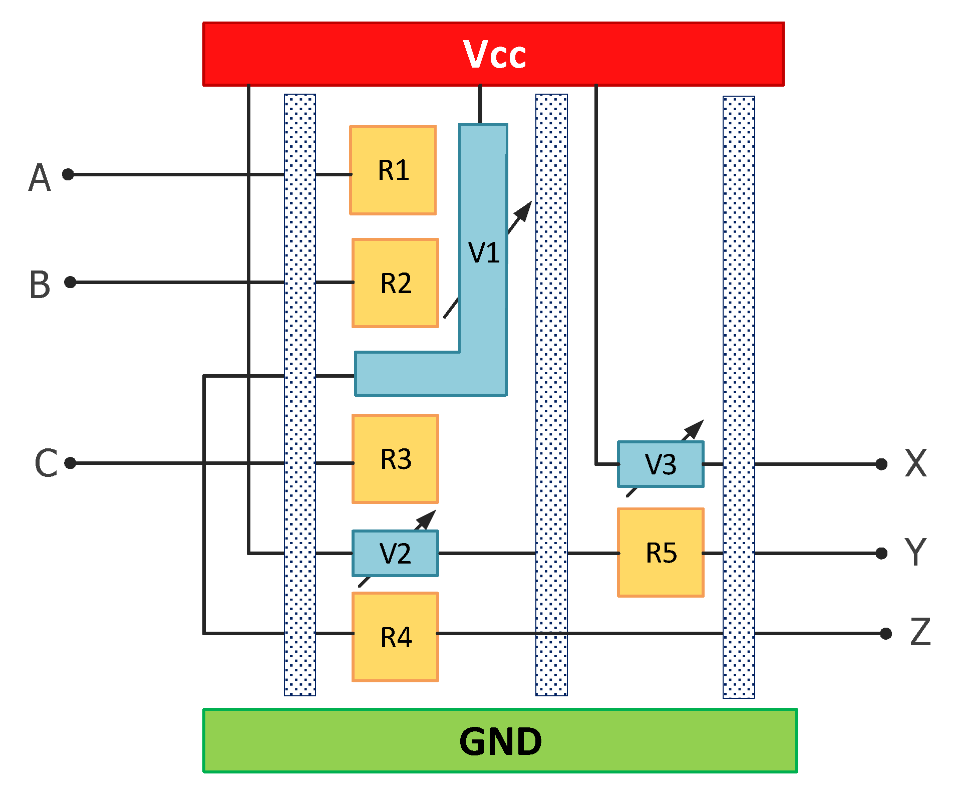
Figure 2 shows a sample TELC structure where R1, R2, R3, R4, and R5 are conventional resistors and V1, V2, and V3 are VO2 SMT resistors. For instance, V1 switches ON if R1 AND R2 are both ON. V2 switches ON if R3 OR R4 is ON. Combinations that are more sophisticated can be implemented by altering the ambient temperature, driving current, elements sizes, distances between the resistors and their locations. When the driving current flows in the conventional resistors, the Joule-heating will heat them and the generated heat will diffuse to the surrounding by convection. With enough heating delivered, VO2 SMT resistors will reach the desired temperature to drop the resistivity value and transition to the conducting phase. This action allows current to pass through VO2 SMT resistors. Furthermore, heat dissipation layers inserted between each section of the structure is important to prevent heat overlapping.
Many problems still need solutions to implement the circuit shown. For example, how the dimensions of an SMT resistor affect the electro-thermal characteristics of the device needs clarification. This paper investigates that how the characteristics of vertical VO2 resistors depend on their sizes by simulation. Previously, we studied lateral structures by performing high-resolution electro-thermal simulations using a range of different dimensions [39]. Measurement results for lateral TELC structures are also available in [40].
The goal of our long-term study is designing and creating real TELC structures that require a comprehensive study of VO2 thin films’ behavior along with how these structures act at different dimensions, arrangements and ambient temperatures. In this article, we examine VO2 based vertical structures at different dimensions.
2. Experimentation
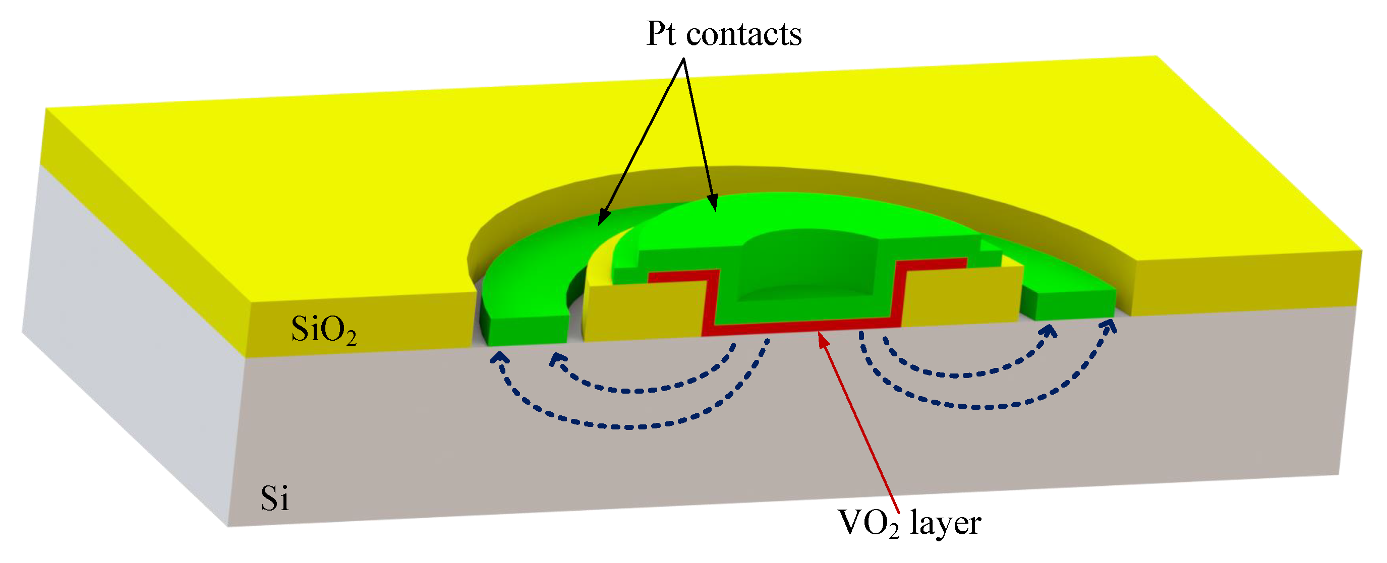
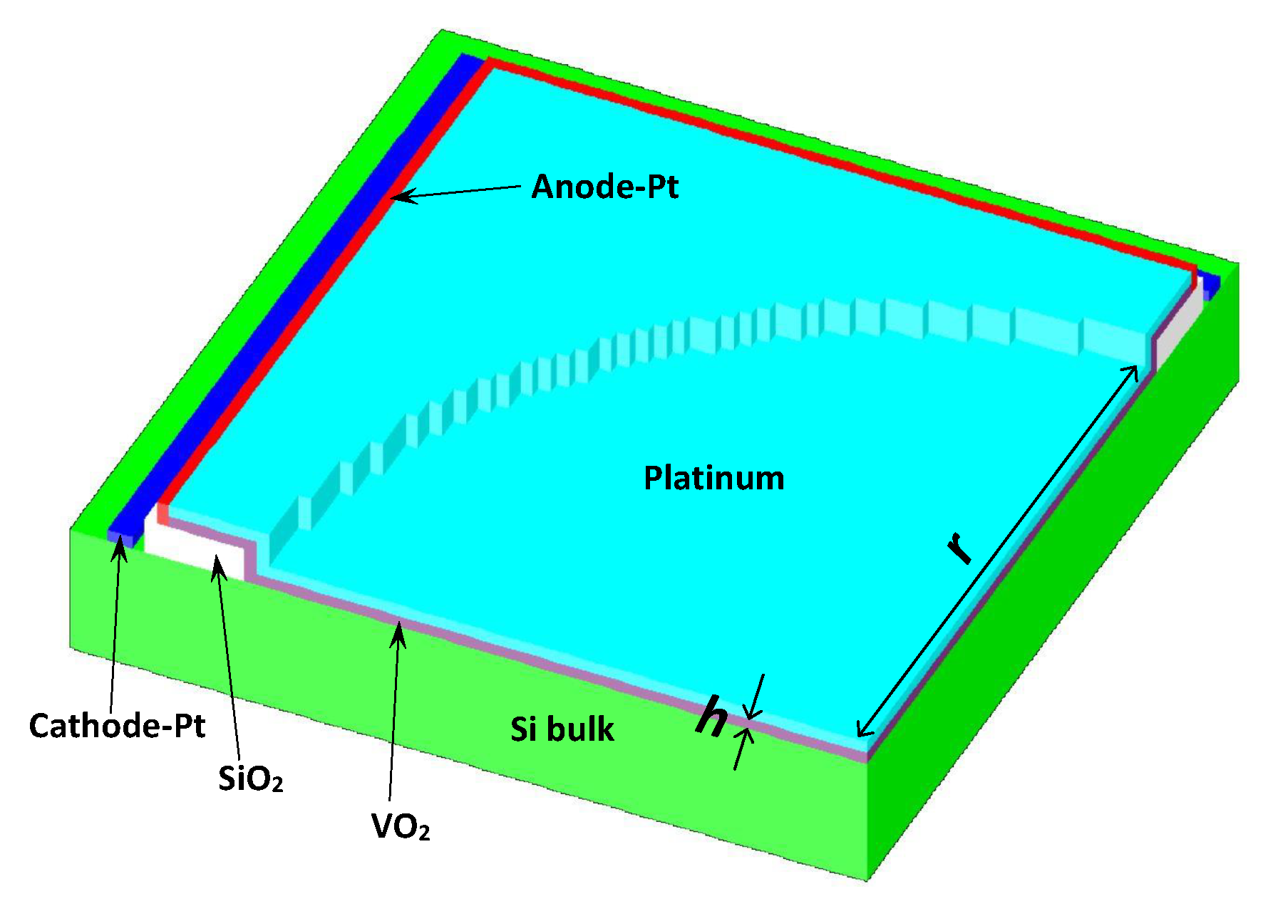
Standard CMOS technology steps were used to prepare the samples for vertical thermo-electrical device test in Figure 3. The substrate was an n-type Si with 3.5 × 1017 cm−3 dopant concentration for better spreading resistance of the vertical structure. The 100 nm SiO2 insulator layer was grown by thermal oxidation. A window was etched into the insulator layer that will be the active conductive channel shape of the vertical structure. The VO2 layer (approximately 50 nm thin) was deposited by RF sputtering at 650 °C high temperature. The radii of the window changed between 10 μm up to 100 μm.
For the tailoring of SMT layer, wet chemistry was applied to remove the surround cover area of the window. The top and collector Pt contacts (approx. 10 nm thin) of devices were also prepared by RF sputtering. Standard optical lithography was applied to transfer the patterns during technology steps. During the vertical structure preparation, lateral structures were prepared to check the SMT layer quality and functional operation. The dimensions of VO2 channels in lateral structures were 100 μm × 700 μm.
Probe station was used for electrical measurement of samples. The electrical measurement was carried out by Keithley SourceMeter and samples were elevated at different environmental temperatures by a Cole-Parmer Thermostat System.
3. Electro-Thermal Simulation
To study thermal-electrical circuits by simulation, a distributed parametric simulator is required, typically with some finite algorithm (FDM, FEM, FVM). The difficulty of simulation is illustrated by the fact that the resistivity of VO2 changes rapidly as a function of temperature (see Figure 1) and the characteristic has a hysteresis.
Steep characteristic is the bigger problem. One consequence of this is developing of more stable working points. Figure 4 shows a VO2 resistor. If a small current is applied to the resistor, whose temperature has increased (because of Joule heating), it does not reach the level required for the phase change, the current density will be of same magnitude throughout the resistor volume. At higher driving currents, the temperature begins to rise. In the part of resistor that first reaches the required temperature for phase change, the resistivity suddenly decreases and the current density increases. In the remaining resistor, however, the current density decreases and thus the temperature also decreases. The positive feedback results in vast majority of current flowing in a hot channel between the anode and cathode. If the material of resistor, structure and environment are homogeneous, the channel forms in the centerline of resistor. However, if this is not the case, the channel may create elsewhere, or even more channels may create. In consequence, a steady-state simulation that takes into account the process of current and temperature distribution must be performed. This example is achieved by time-domain simulation.
The structure of the device shown in Figure 4 and the boundary conditions of the simulation are the same as those of the device shown in [41]. The 200 μm × 20 μm × 0.5 μm VO2 resistor is directly connected to the platinum anode and cathode. There was 25 °C air above the device, and the bottom was connected to a cold plate at 50 °C. In the simulation, the driving current was increased in 2 increments up to 20 and then decreased in the same increments to 0. The temperature distribution is shown in Figure 4b is for the increasing 2 , while the distribution is shown in Figure 4c is for the decreasing 8 . In [41], the process of channel formation and termination can be viewed in a series of images.
Another problem arising from the steep characteristic is that the simulation is difficult to converge. In the literature, we find that either electro-thermal simulation results for very specific VO2 structures [29,42], or they achieve the convergence by applying special boundary conditions [43]. In the case of thermal-electrical circuits, these solutions cannot be applied. Our attempts with ANSYS ended in failure, so we made the custom, finite volumes method based simulator developed at the department suitable for handling the special properties of vanadium dioxide [41].
3.1. Computational Method (SUNRED)
In the custom simulator, the examined structure divides by a grid into elementary rectangular cells and each cell is filled with a homogeneous material see Figure 5a. The real structure is three-dimensional as the figure shows a layer of it for clarity. The elementary cells are modeled by a circuit. Adjacent elementary cells are connected by an electrical and a thermal line (the ground is not marked), as shown in Figure 5b. The model obtained from the finite volume method gives the internal structure of elementary cells [44].
A typical structure is shown in Figure 5c. Dissipation caused by current flowing in the electrical part is realized by the dependent power source of the thermal model. Electrical and thermal circuit elements are temperature dependent. The computational task is to determine the voltages and temperatures with knowledge of the excitations and boundary conditions. The simulator performs the solution by successive network reduction method (SUNRED). Figure 5d, which merges cell pairs in each step, knocks out the internal nodes from the equations until finally, a single cell remains. The boundary conditions are applied to this cell, and then the voltages and temperatures of the internal nodes are calculated in a series of successive backward substitution steps.
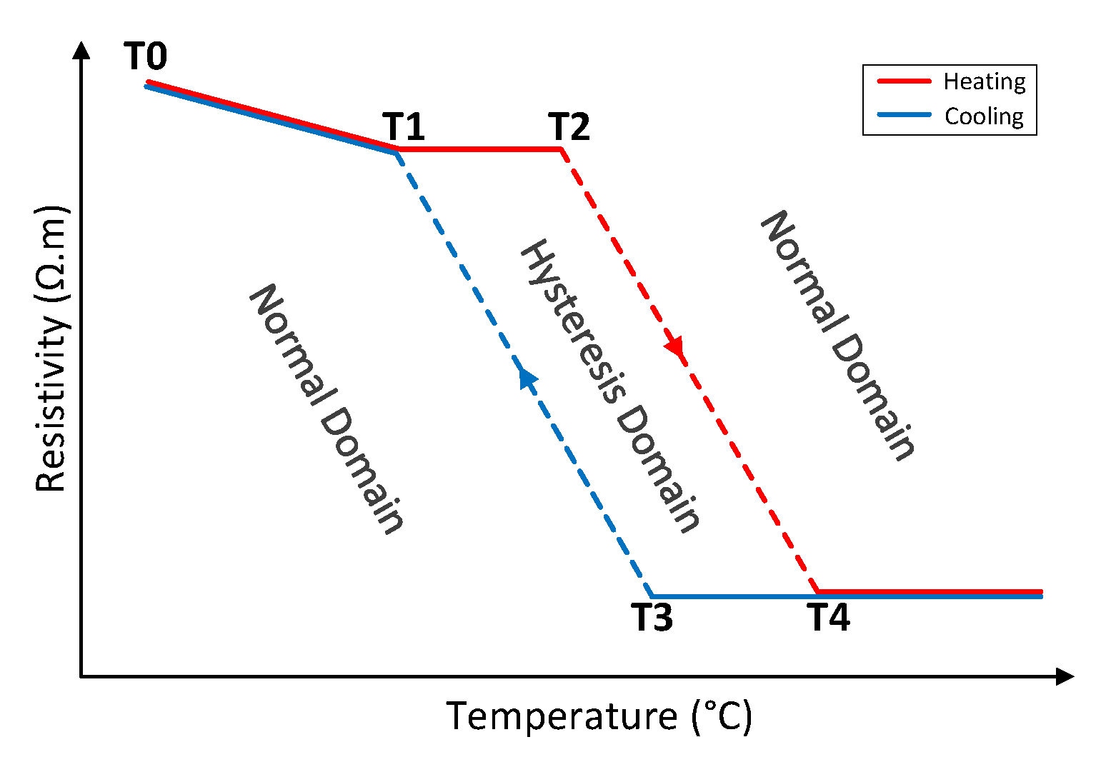
In the time domain, the solution is done by the backward Euler method, and the nonlinear calculation is by successive approximation. A heuristic method is used to deal with the extreme nonlinearity of VO2, details of which are described in [41]. Having more than one value of resistivity at one temperature value, in addition to the memory effect in VO2, make the hysteresis loop essential in the materials resistivity function. The hysteresis of the resistivity of VO2 is modeled by a parallelogram, see Figure 6.
3.2. Hysteresis Model
The resistivity function consists of two domains in SUNRED, normal domain and hysteresis domain. In the hysteresis domain, resistivity is multi-valued and any resistance-temperature combination can occur, not just the edges. For instance, when the structure temperature is raised starting from the room temperature 25 °C, resistivity drops linearly in the temperature range (T0 = 25 °C, T1 = 58 °C). In the following temperature range (T1 = 58 °C, T2 = 64 °C), resistivity remains constant in the hysteresis domain. The material phase change begins above T2 and hence triggers the semiconductor-to-metal transition. SMT leads to a sharp drop in resistivity in the temperature range (T2 = 64 °C, T4 = 73 °C). At 73 °C, the material encounters a full phase transition and resistivity above this temperature is always constant. If the temperature between T2 and T4 starts to decrease, the resistivity remains constant until it reaches the T3-T1 section. It then goes to section T3-T1 to T1 and then T0. During the cooling phase, resistivity function does not follow the same pattern as the heating phase because of the hysteresis. It remains constant until reaching T3 = 67 °C. A reverse phase change occurs in the temperature range (T3 = 67 °C, T1 = 58 °C), bringing VO2 back to the nonconductive state. Resistivity moves up linearly on further reduction of temperature [41].
3.3. Geometry of the Simulated Structure
An equivalent geometry of our vertical structure in Figure 7 is built in the SUNRED simulator (r = 10 μm, h = 50 nm). The VO2 layer is sandwiched between platinum and silicon layers. The silicon substrate layer is 6.2 mm × 6.2 mm and 0.3 mm thickness. For faster simulations and simplicity, the quarter of the entire geometry is simulated. In this case, electric current must be multiplied by four while describing the full structure and the cavity length (r) represents the radius of the whole cavity. The bottom of the substrate (the bottom boundary condition) is a heat transfer coefficient (HTC) specified in Section 4. All other sides have a boundary condition of 10 W/m2 K (the value for air).
3.4. Excitation Required for the Simulation
SUNRED capabilities allow different methods for creating excitation in the simulated structure. Electrical current, power (heat flow), voltage and temperature are the available options. For our study, we use electric current on the anode as excitation for the structure. The principal is to assign a different current value in each simulation step. Setting the cathode as the electric ground of the geometry (electric potential = zero) initiates the direction of the electric current from anode to cathode. Optimal path for the current is to pass through VO2 and Si, reaching the cathode and creating the current flow because air and SiO2 have high resistivity (refer to Figure 3).
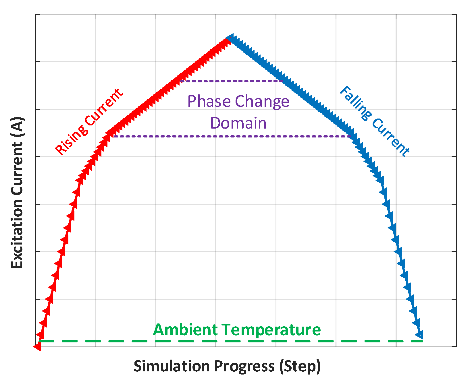
The simulation starts with a low excitation current and gradual increase in each step. Driving current warms up VO2 layer above the ambient temperature (50 °C) due to the generation of Joule-heat. Higher excitation current leads to a higher temperature of VO2 resistor and further elevation of temperature is required to simulate the phase-change of VO2. A similar excitation current profile is used for the second half of the simulation but with a falling direction instead of rising, Figure 8. The peak value and difference of excitation current in each step can be modified to improve the resolution. Smaller current steps give higher resolution.
4. Results and Discussion
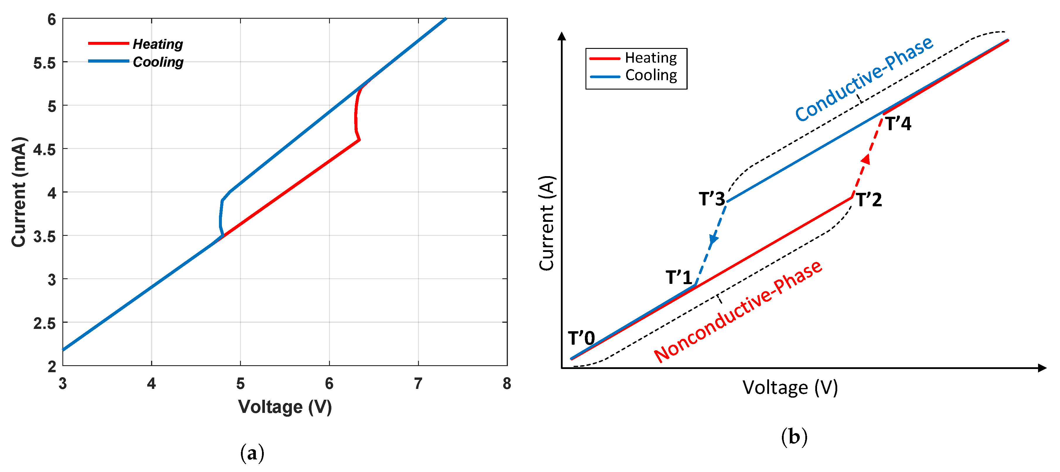
Each flow of current accompanies an electric voltage developed between anode and cathode. (Voltage, Current) pair in each step is gathered to draw the V-I characteristic curve of our structure. For instance, the V-I curve for one of the performed simulations on vertical VO2 resistors is shown in Figure 9a. The simulated geometry is (r = 10 μm, h = 60 nm) and the ambient temperature is 50 °C. After analyzing several V-I characteristics, a general visualization of the V-I curve of vertical VO2 geometries can be formalized as illustrated in Figure 9b.
The starting point of the study is to simulate the geometry in Figure 7 using the real size of produced sample in laboratory (r = 10 μm, h = 50 nm). The low-current section of the measured curve is strongly nonlinear, which did not occur in case of lateral SMT resistors [40,41]. The main difference between the current vertical structure and the previously studied lateral structures is that in lateral structures the platinum anode and cathode were directly attached to VO2, while in the vertical structure the silicon substrate was inserted between the cathode and VO2.
More than 90% of the voltage applied to the entire structure drops in the region between the cathode and the VO2 resistor even when the VO2 resistor is OFF. The three main parts of the region are the platinum-silicon transition at the cathode, the substrate, and the silicon-VO2 transition. Since the doping of the substrate is high, its resistivity is around , the voltage on it is only a fraction of the voltage applied to the region. In addition, the temperature-dependent nonlinearity of the substrate is very low [45], it cannot be responsible for the measured nonlinearity. The Pt-Si interface can show a Shottky like barrier which will depend on the Si dopant concentration [46]. Annealing could create a platinum-silicide transition that would give an ohmic contact, however, annealing cannot be applied due to VO2. Based on the band structure of VO2 [47], it is likely that a barrier will also be created at the junction of the two semiconductor materials. Most of the voltage in the region, therefore, drops at the two transitions.
Based on the measured results, the current dependence on resistivity of the transitions is mainly responsible for the nonlinearity, the temperature dependence is not significant, because at higher currents the curve is almost linear. Since the purpose is the investigation of size dependence of VO2 resistor at higher currents, the simulation is greatly simplified if nonlinearity is not taken into account and the transitions are modeled with constant resistivity. Accordingly, in the simulated model, a 100 nm thick resistor layer has been placed between both the Pt-Si and Si-VO2 interfacing surfaces.
Three cases were examined: (a) if a barrier is assumed only at the Pt-Si transition, (b) if a barrier is assumed only at the Si-VO2 transition and (c) if barriers are assumed at both transitions with same voltage drops. In case (a) the resistivity of the layer between Pt-Si is 1.33 × 10⁵ and the at the bottom of the substrate is 46 W/m2 K; in case (b), the resistivity of the layer between Si-VO2 is 377 and the at the bottom of the substrate is 100 W/m2 K; and in case (c), the resistivity of the layer between Pt-Si is 6.7 × 10⁴ , between Si-VO2 it is 189 and the HTC is 60 W/m2 K. Results of the three simulations are shown in Figure 10b.
Both curves show an acceptable degree of validity. However, it is difficult to reach a near-absolute accuracy while neglecting the nonlinearity of the transitions. The location of the resistor defines the dissipation point. From circuitry point of view, the three cases are equivalent. We assume that there is a barrier at both transitions, so in the rest of the article, we perform the simulations with the model corresponding to case (c).
The experimental data in Figure 10a show a “noisy” behavior in the ascending current phase. When the current increases through the SMT layer, some conductive channels are switched ON, which as a consequense gives the noisy path. When the current decreases, the SMT conductive channel collapse faster. This phenomenon can also be observed with decreasing current, but it is much more moderated than with the increasing current case. The origin of the noisy signal is that a lot of parallel conductive channels are in the SMT layer (depends on the crystal structure). The real VO2 layer is not a homogenous crystal, it has a spiky structure [48]. While input power increases, some of the conductive channels are “switched ON”, which are connected in parallel with the original SMT phase. If the dissipated power decreases (the resistance decreases) then it can switch back, which shows a jump back to the original path. This phenomenon also appears in other structures, for example in [40], the lateral structure with two Pt contacts are directly attached to VO2, no Si substrate is interposed.
4.1. Dependence on Thickness
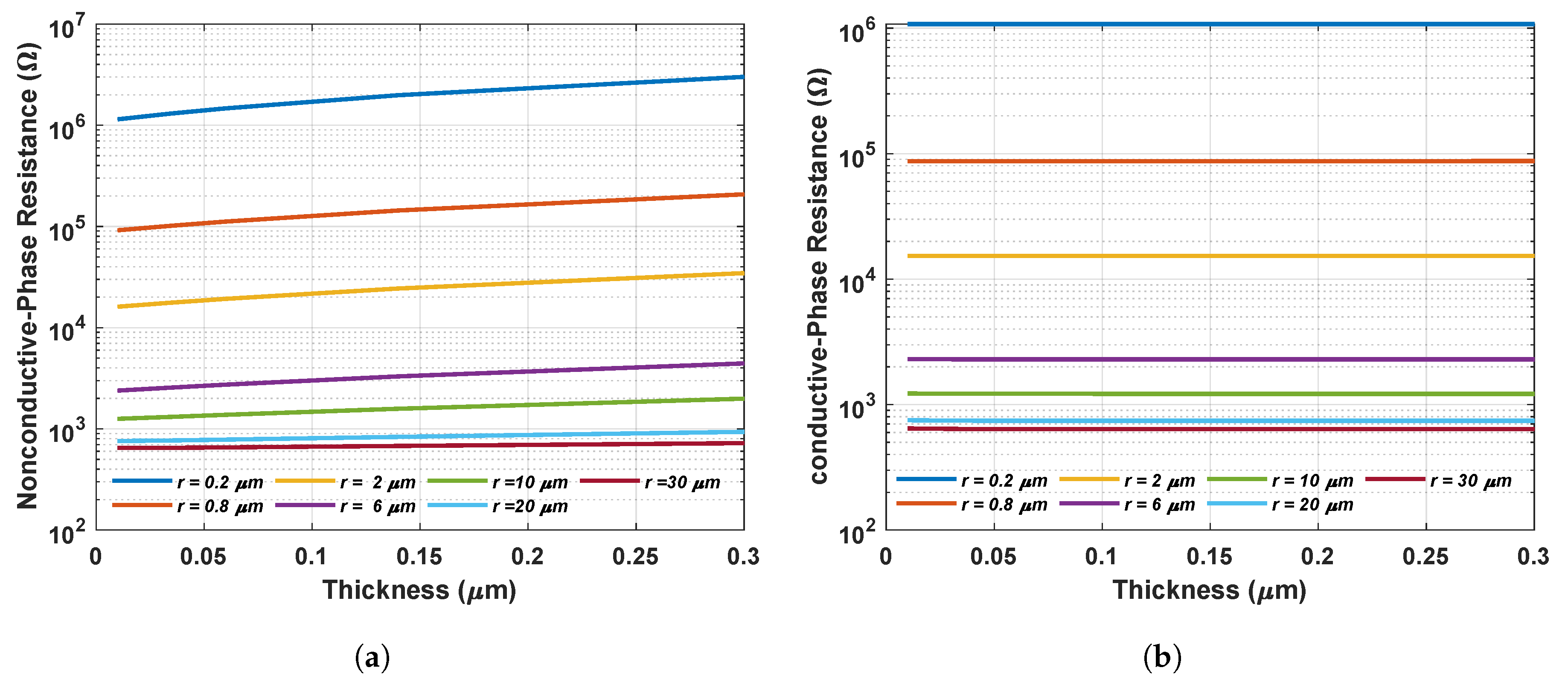
In the first set of simulations, we investigated how the VO2 structure behaves on different thicknesses and what is the effect of changing h on the characteristics of our structure. The range of h used in the simulations is (10 to 300 ) which is investigated at different radii. Figure 11 shows how the resistance (R) of VO2 layer changes with thickness. Resistance during the nonconductive and conductive phases is the point of interest here (refer to Figure 9b). Resistance is calculated as the of the V-I curve. It can be concluded from Figure 11a that the nonconductive phase resistance increases as thickness increases. Furthermore, R dependence on h becomes lower at larger radii. On the other hand, conductive phase resistance shows no direct relation with thickness at these h and r ranges, Figure 11b.
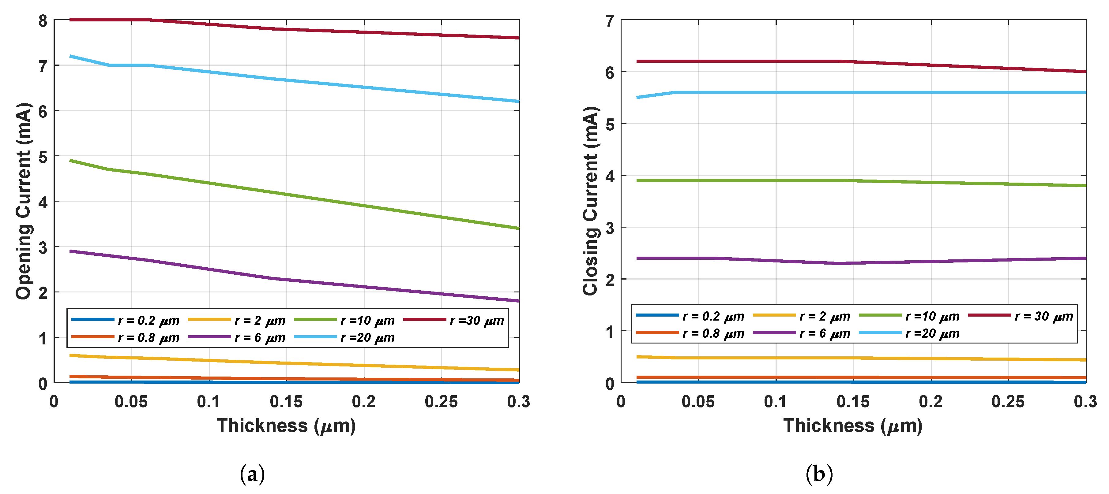
The current at which VO2 resistor is turned on (when resistivity drops significantly) is called the opening current. Similarly, the current at which the VO2 resistor is turned off (during the cooling phase) is called the closing current. Voltages associated with these currents are opening voltage and closing voltage, respectively. Figure 12 illustrates the dependence of opening and closing currents on the variation of thickness. Since the opening current is associated with the nonconductive phase resistance and the closing current is associated with the conductive phase resistance, the opening current falls as thickness increases due to the elevation of R versus thickness (in the nonconductive phase), Figure 12a. On the other hand, the current remains unchanged as thickness increases because resistance is not affected by thickness (in the conductive phase), Figure 12b. A high degree of compatibility can be noticed between Figure 11 and Figure 12.
4.2. Dependence on Radius
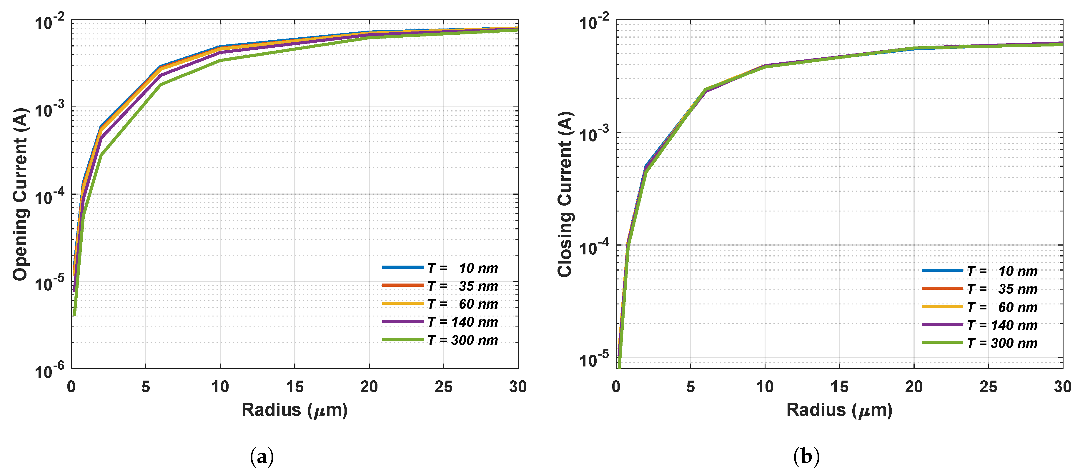
The second set of simulations is to study how the structure responds to change in radius. Simulations performed with different radii r in the range of (200 nm to 30 μm) and are investigated at different thicknesses. Figure 13 concludes that radius has a strong effect on the VO2 resistance, and the resistance drops nonlinearly for both the nonconductive phase (Figure 13a) and the conductive phase (Figure 13b) as radius increases. It is explained with the relation , is the resistivity, l is length (which is h here) and A is the cross-sectional area (which is here ).
As a consequence of the resistance dependence on radius, opening and closing currents increase as radius increases. Figure 14 illustrates the effect of changing the radius on the opening current (Figure 14a) and the closing current (Figure 14b). For low current applications, it is worth to consider decreasing the radius since it allows the phase change to occur at much lower currents.
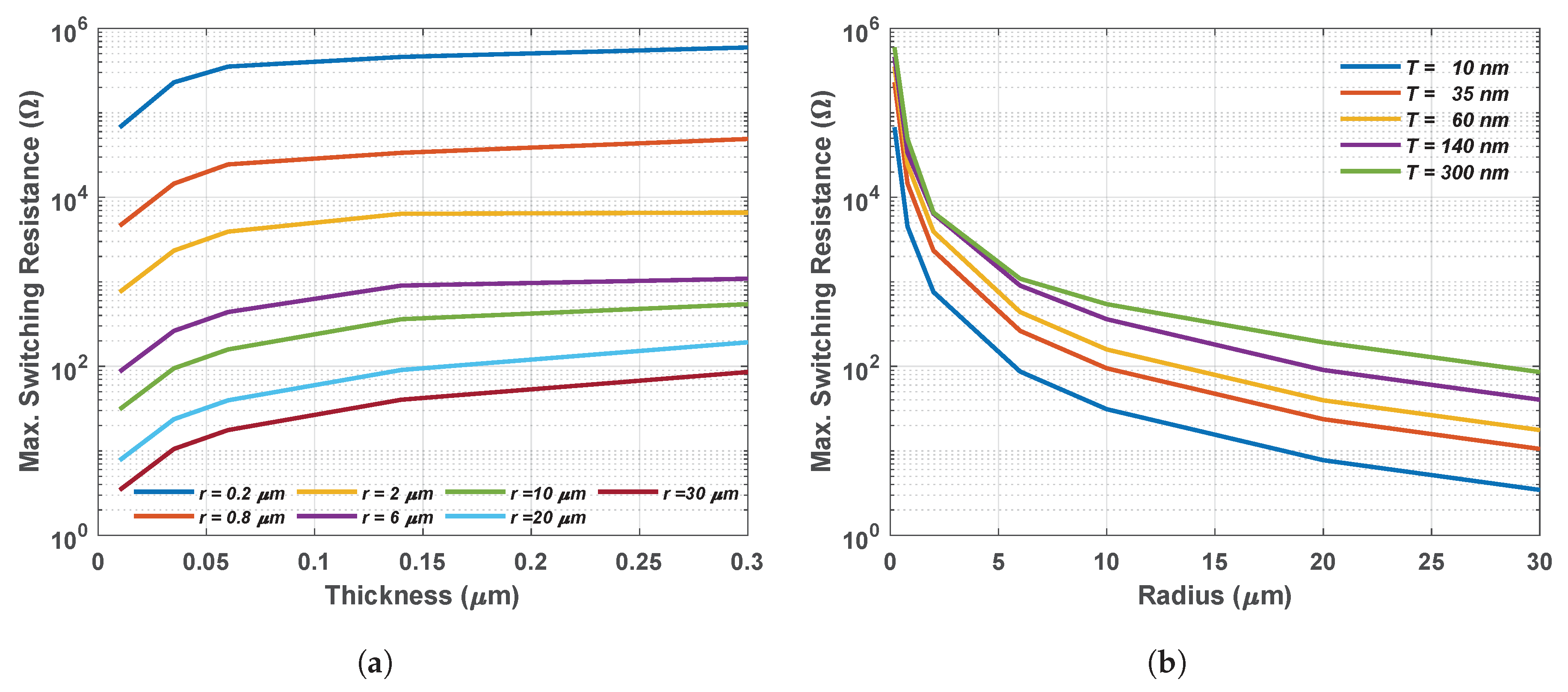
During the hysteresis domain, the resulting V-I curve also has hysteric nature (refer to Figure 9b). Maximum difference between the resistance of VO2 resistor during heating and cooling phases is called the maximum switching resistance. It can be observed that the maximum switching resistance varies linearly versus thickness Figure 15a, in contrast, it has a nonlinear dependence on the radius Figure 15b.
5. Conclusions
The results of this article offer a good base of sample sizes estimates for further studies in submicron modeling of VO2 resistors. A valid operating model will pave the way for designing thermal-electronic logic circuits. The results provided in our previous work [39] about the lateral structures and results of this article about the vertical structures will straiten the range of samples sizes for producing and studying. This will save both time and effort.
Author Contributions
Conceptualization, P.N. and M.D.; methodology, M.D.; software, L.P.; validation, M.D.; technology, J.M.; sample creation and measurement, P.N.; writing—original draft preparation, M.D., L.P., P.N.; writing—review and editing, L.P., M.D.; visualization, M.D.; supervision, L.P.; project administration, J.M.; funding acquisition, P.N. All authors have read and agreed to the published version of the manuscript.
Funding
The research reported in this paper and carried out at the Budapest University of Technology and Economics was supported by the “TKP2020, National Challenges Program” of the National Research Development and Innovation Office (BME NC TKP2020). This research also received fund by the Higher Education Excellence Program of the Ministry of Human Capacities in the frame of Nanotechnology research area of the Budapest University of Technology and Economics (BME FIKP-NANO) and the Science Excellence Program at BME under the grant agreement NKFIH-849-8/2019 of the Hungarian National Research, Development and Innovation Office is also acknowledged. The research reported in this paper was partially supported by the Stipendium Hungaricum Scholarship Programme of the Hungarian Government.
Conflicts of Interest
The authors declare no conflict of interest. The funders had no role in the design of the study; in the collection, analyses, or interpretation of data; in the writing of the manuscript, or in the decision to publish the results.
Abbreviations
The following abbreviations are used in this manuscript:
| VO2 | Vanadium dioxide |
| CMOS | Complementary metal–oxide–semiconductor |
| TELC | Thermal-electronic logic circuits |
| SMT | Semiconductor-to-metal transition |
| Si | Silicon |
| SiO2 | Silicon dioxide |
| RF | Radio frequency |
| Pt | Platinum |
| FDM | Finite difference method |
| FEM | Finite element method |
| FVM | Finite volume method |
| HTC | Heat transfer coefficient |
| SUNRED | Successive network reduction method (also the simulator name) |
References
- Shalf, J. The future of computing beyond Moore’s Law. Philos. Trans. R. Soc. A Math. Phys. Eng. Sci. 2020, 378, 20190061. [Google Scholar] [CrossRef] [PubMed] [Green Version]
- Markov, I.L. Limits on fundamental limits to computation. Nature 2014, 512, 147–154. [Google Scholar] [CrossRef] [Green Version]
- Shalf, J.M.; Leland, R. Computing beyond Moore’s Law. Computer 2015, 48, 14–23. [Google Scholar] [CrossRef]
- Joneckis, L.; Koester, D.; Alspector, J. An Initial Look at Alternative Computing Technologies for the Intelligence Community; Technical Report; Institute for Defense Analyses: Alexandria, VA, USA, 2014. [Google Scholar]
- Thompson, N.; Spanuth, S. The Decline of Computers As a General Purpose Technology: Why Deep Learning and the End of Moore’s Law are Fragmenting Computing. SSRN Electron. J. 2018. [Google Scholar] [CrossRef] [Green Version]
- Jouppi, N.P.; Young, C.; Patil, N.; Patterson, D.; Agrawal, G.; Bajwa, R.; Bates, S.; Bhatia, S.; Boden, N.; Borchers, A.; et al. In-Datacenter Performance Analysis of a Tensor Processing Unit. In Proceedings of the 44th Annual International Symposium on Computer Architecture; ACM: New York, NY, USA, 2017; pp. 1–12. [Google Scholar] [CrossRef] [Green Version]
- Caulfield, A.M.; Chung, E.S.; Putnam, A.; Angepat, H.; Fowers, J.; Haselman, M.; Heil, S.; Humphrey, M.; Kaur, P.; Kim, J.Y.; et al. A cloud-scale acceleration architecture. In Proceedings of the 2016 49th Annual IEEE/ACM International Symposium on Microarchitecture (MICRO), Taipei, Taiwan, 15–19 October 2016; pp. 1–13. [Google Scholar] [CrossRef]
- Hill, M.D.; Reddi, V.J. Accelerator-level Parallelism. arXiv 2019, arXiv:1907.02064. [Google Scholar]
- Ingerly, D.B.; Enamul, K.; Gomes, W.; Jones, D.; Kolluru, K.C.; Kandas, A.; Kim, G.S.; Ma, H.; Pantuso, D.; Petersburg, C.; et al. Foveros: 3D Integration and the use of Face-to-Face Chip Stacking for Logic Devices. In Proceedings of the 2019 IEEE International Electron Devices Meeting (IEDM), San Francisco, CA, USA, 7–11 December 2019; pp. 19.6.1–19.6.4. [Google Scholar] [CrossRef]
- Nikonov, D.E.; Young, I.A. Overview of Beyond-CMOS Devices and a Uniform Methodology for Their Benchmarking. Proc. IEEE 2013, 101, 2498–2533. [Google Scholar] [CrossRef] [Green Version]
- Seabaugh, A.C.; Zhang, Q. Low-Voltage Tunnel Transistors for Beyond CMOS Logic. Proc. IEEE 2010, 98, 2095–2110. [Google Scholar] [CrossRef]
- Low, T.; Appenzeller, J. Electronic transport properties of a tilted graphene p-n junction. Phys. Rev. B 2009, 80, 155406. [Google Scholar] [CrossRef] [Green Version]
- Banerjee, S.; Register, L.; Tutuc, E.; Reddy, D.; MacDonald, A. Bilayer PseudoSpin Field-Effect Transistor (BiSFET): A Proposed New Logic Device. IEEE Electron Device Lett. 2009, 30, 158–160. [Google Scholar] [CrossRef]
- Sugahara, S.; Tanaka, M. A spin metal–oxide–semiconductor field-effect transistor using half-metallic-ferromagnet contacts for the source and drain. Appl. Phys. Lett. 2004, 84, 2307–2309. [Google Scholar] [CrossRef] [Green Version]
- Currivan, J.A.; Jang, Y.; Mascaro, M.D.; Baldo, M.A.; Ross, C.A. Low Energy Magnetic Domain Wall Logic in Short, Narrow, Ferromagnetic Wires. IEEE Magn. Lett. 2012, 3, 3000104. [Google Scholar] [CrossRef]
- Nikonov, D.E.; Bourianoff, G.I.; Ghani, T. Proposal of a Spin Torque Majority Gate Logic. IEEE Electron Device Lett. 2011, 32, 1128–1130. [Google Scholar] [CrossRef] [Green Version]
- Behin-Aein, B.; Datta, D.; Salahuddin, S.; Datta, S. Proposal for an all-spin logic device with built-in memory. Nat. Nanotechnol. 2010, 5, 266–270. [Google Scholar] [CrossRef]
- Mizsei, J.; Lappalainen, J.; Bein, M.C. Thermal-electronic integrated logic. In Proceedings of the 19th International Workshop on Thermal Investigations of ICs and Systems (THERMINIC), Berlin, Germany, 25–27 September 2013; pp. 128–134. [Google Scholar] [CrossRef]
- Zylbersztejn, A.; Mott, N.F. Metal-insulator transition in vanadium dioxide. Phys. Rev. B 1975, 11, 4383–4395. [Google Scholar] [CrossRef] [Green Version]
- Limelette, P. Universality and Critical Behavior at the Mott Transition. Science 2003, 302, 89–92. [Google Scholar] [CrossRef] [PubMed] [Green Version]
- Lappalainen, J.; Heinilehto, S.; Jantunen, H.; Lantto, V. Electrical and optical properties of metal-insulator-transition VO2 thin films. J. Electroceram. 2009, 22, 73–77. [Google Scholar] [CrossRef]
- Chain, E.E. Optical properties of vanadium dioxide and vanadium pentoxide thin films. Appl. Opt. 1991, 30, 2782. [Google Scholar] [CrossRef]
- Rozgonyi, G.A.; Hensler, D.H. Structural and Electrical Properties of Vanadium Dioxide Thin Films. J. Vac. Sci. Technol. 1968, 5, 194–199. [Google Scholar] [CrossRef]
- Budai, J.D.; Hong, J.; Manley, M.E.; Specht, E.D.; Li, C.W.; Tischler, J.Z.; Abernathy, D.L.; Said, A.H.; Leu, B.M.; Boatner, L.A.; et al. Metallization of vanadium dioxide driven by large phonon entropy. Nature 2014, 515, 535–539. [Google Scholar] [CrossRef]
- Qazilbash, M.M.; Brehm, M.; Chae, B.G.; Ho, P.C.; Andreev, G.O.; Kim, B.J.; Yun, S.J.; Balatsky, A.V.; Maple, M.B.; Keilmann, F.; et al. Mott Transition in VO2 Revealed by Infrared Spectroscopy and Nano-Imaging. Science 2007, 318, 1750–1753. [Google Scholar] [CrossRef] [Green Version]
- Kim, H.T.; Lee, Y.W.; Kim, B.J.; Chae, B.G.; Yun, S.J.; Kang, K.Y.; Han, K.J.; Yee, K.J.; Lim, Y.S. Monoclinic and correlated metal phase in VO2 as evidence of the Mott transition: Coherent phonon analysis. Phys. Rev. Lett. 2006, 97, 266401. [Google Scholar] [CrossRef] [Green Version]
- Gomez-Heredia, C.L.; Ramirez-Rincon, J.A.; Ordonez-Miranda, J.; Ares, O.; Alvarado-Gil, J.J.; Champeaux, C.; Dumas-Bouchiat, F.; Ezzahri, Y.; Joulain, K. Thermal hysteresis measurement of the VO2 emissivity and its application in thermal rectification. Sci. Rep. 2018, 8, 8479. [Google Scholar] [CrossRef] [Green Version]
- Hamaoui, G.; Horny, N.; Gomez-Heredia, C.L.; Ramirez-Rincon, J.A.; Ordonez-Miranda, J.; Champeaux, C.; Dumas-Bouchiat, F.; Alvarado-Gil, J.J.; Ezzahri, Y.; Joulain, K.; et al. Thermophysical characterisation of VO2 thin films hysteresis and its application in thermal rectification. Sci. Rep. 2019, 9, 8728. [Google Scholar] [CrossRef] [Green Version]
- Hu, B.; Zhang, Y.; Chen, W.; Xu, C.; Wang, Z.L. Self-heating and External Strain Coupling Induced Phase Transition of VO2 Nanobeam as Single Domain Switch. Adv. Mater. 2011, 23, 3536–3541. [Google Scholar] [CrossRef] [PubMed]
- Soltani, M.; Chaker, M.; Haddad, E.; Kruzelesky, R.V. Thermochromic vanadium dioxide smart coatings grown on Kapton substrates by reactive pulsed laser deposition. J. Vac. Sci. Technol. A Vac. Surf. Films 2006, 24, 612–617. [Google Scholar] [CrossRef]
- Datta, S.; Shukla, N.; Cotter, M.; Parihar, A.; Raychowdhury, A. Neuro Inspired Computing with Coupled Relaxation Oscillators. In Proceedings of the The 51st Annual Design Automation Conference on Design Automation Conference—DAC’14; ACM Press: New York, NY, USA, 2014; pp. 1–6. [Google Scholar] [CrossRef]
- Zhou, Y.; Ramanathan, S. Mott Memory and Neuromorphic Devices. Proc. IEEE 2015, 103, 1289–1310. [Google Scholar] [CrossRef] [Green Version]
- Ordonez-Miranda, J.; Ezzahri, Y.; Drevillon, J.; Joulain, K. Dynamical heat transport amplification in a far-field thermal transistor of VO2 excited with a laser of modulated intensity. J. Appl. Phys. 2016, 119, 203105. [Google Scholar] [CrossRef]
- Prod’Homme, H.; Ordonez-Miranda, J.; Ezzahri, Y.; Drevillon, J.; Joulain, K. VO2 -based radiative thermal transistor in the static regime 2017. arXiv 2017, arXiv:1710.10332. [Google Scholar]
- Chen, C.; Zhao, Y.; Pan, X.; Kuryatkov, V.; Bernussi, A.; Holtz, M.; Fan, Z. Influence of defects on structural and electrical properties of VO2 thin films. J. Appl. Phys. 2011, 110, 023707. [Google Scholar] [CrossRef]
- Jian, J.; Chen, A.; Zhang, W.; Wang, H. Sharp semiconductor-to-metal transition of VO2 thin films on glass substrates. J. Appl. Phys. 2013, 114, 244301. [Google Scholar] [CrossRef]
- Taha, M.; Walia, S.; Ahmed, T.; Headland, D.; Withayachumnankul, W.; Sriram, S.; Bhaskaran, M. Insulator—Metal transition in substrate-independent VO2 thin film for phase-change devices. Sci. Rep. 2017, 7, 17899. [Google Scholar] [CrossRef] [PubMed]
- Mizsei, J.; Bein, M.; Lappalainen, J.; Juhász, L.; Plesz, B. The Phonsistor—A Novel VO2 Based Nanoscale Thermal-electronic Device and Its Application in Thermal-electronic Logic Circuits (TELC). Mater. Today Proc. 2015, 2, 4272–4279. [Google Scholar] [CrossRef]
- Pohl, L.; Darwish, M.; Mizsei, J. Electro-Thermal Investigation of SMT Resistors for Thermal-Electrical Logic Circuits by Simulation. In Proceedings of the 2019 25th International Workshop on Thermal Investigations of ICs and Systems (THERMINIC), Lecco, Italy, 25–27 September 2019; pp. 1–4. [Google Scholar] [CrossRef]
- Mizsei, J.; Lappalainen, J. Microelectronics, Nanoelectronics: Step behind the red brick wall using the thermal domain. Mater. Today Proc. 2019, 7, 888–893. [Google Scholar] [CrossRef]
- Pohl, L.; Ur, S.; Mizsei, J. Thermoelectrical modelling and simulation of devices based on VO2. Microelectron. Reliab. 2017, 79, 387–394. [Google Scholar] [CrossRef]
- Gopalakrishnan, G.; Ruzmetov, D.; Ramanathan, S. On the triggering mechanism for the metal–insulator transition in thin film VO2 devices: Electric field versus thermal effects. J. Mater. Sci. 2009, 44, 5345–5353. [Google Scholar] [CrossRef]
- Kumar, S.; Pickett, M.D.; Strachan, J.P.; Gibson, G.; Nishi, Y.; Williams, R.S. Local Temperature Redistribution and Structural Transition During Joule-Heating-Driven Conductance Switching in VO2. Adv. Mater. 2013, 25, 6128–6132. [Google Scholar] [CrossRef] [Green Version]
- Nagy, G.; Horváth, P.; Pohl, L.; Poppe, A. Advancing the thermal stability of 3D ICs using logi-thermal simulation. Microelectron. J. 2015, 46, 1114–1120. [Google Scholar] [CrossRef]
- PV Lighthouse: Resistivity Calculator. Available online: https://www.pvlighthouse.com.au (accessed on 21 June 2020).
- Muta, H. Electrical Properties of Platinum-Silicon Contact Annealed in an H 2 Ambient. Jpn. J. Appl. Phys. 1978, 17, 1089–1098. [Google Scholar] [CrossRef]
- Martens, K.; Radu, I.P.; Mertens, S.; Shi, X.; Nyns, L.; Cosemans, S.; Favia, P.; Bender, H.; Conard, T.; Schaekers, M.; et al. The VO2 interface, the metal-insulator transition tunnel junction, and the metal-insulator transition switch On-Off resistance. J. Appl. Phys. 2012, 112, 124501. [Google Scholar] [CrossRef]
- Rao Popuri, S.; Artemenko, A.; Labrugere, C.; Miclau, M.; Villesuzanne, A.; Pollet, M. VO2 (A): Reinvestigation of crystal structure, phase transition and crystal growth mechanisms. J. Solid State Chem. 2014, 213, 79–86. [Google Scholar] [CrossRef]
Figure 1.
Temperature dependence of the resistivity of vanadium dioxide for (100) VO2; based on [20].
Figure 1.
Temperature dependence of the resistivity of vanadium dioxide for (100) VO2; based on [20].

Figure 2.
Implementation of VO2 thermal switching in a TELC circuit.

Figure 3.
Cross-sectional view of the vertical VO2 structure prepared in the lab.

Figure 4.
A 200 μm × 20 μm × 0.5 μm VO2 resistor: (a) Structure; (b) Temperature distribution at low current (2 mA); (c) Temperature distribution at high current (8 mA).
Figure 4.
A 200 μm × 20 μm × 0.5 μm VO2 resistor: (a) Structure; (b) Temperature distribution at low current (2 mA); (c) Temperature distribution at high current (8 mA).
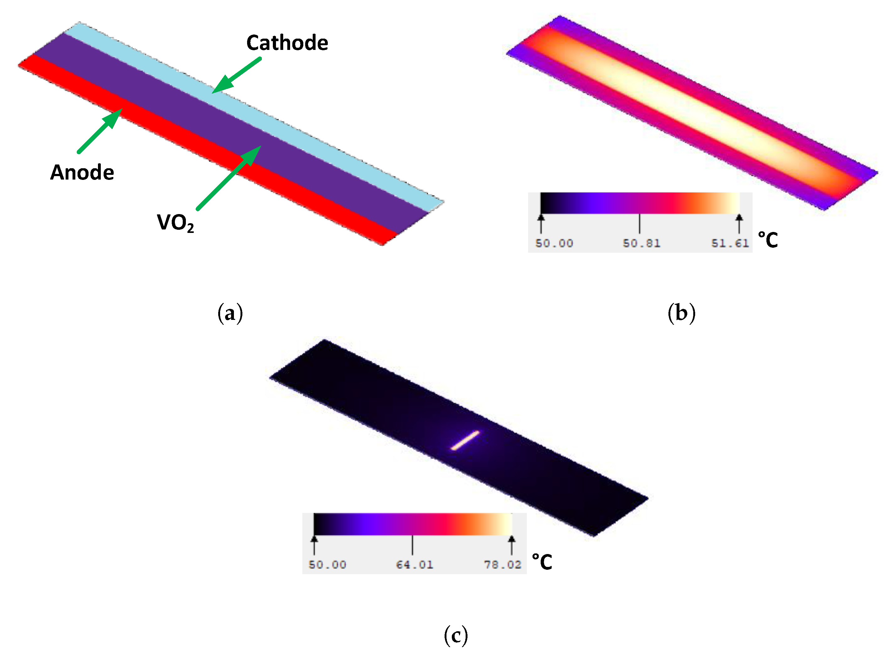
Figure 5.
Operation of the custom solver (for clarity in 2D): (a) Dividing the model into elementary cells; (b) Model network built from elementary cells; (c) Electro-thermal elementary cell, red: thermal, blue: electrical; (d) Successive network reduction.
Figure 5.
Operation of the custom solver (for clarity in 2D): (a) Dividing the model into elementary cells; (b) Model network built from elementary cells; (c) Electro-thermal elementary cell, red: thermal, blue: electrical; (d) Successive network reduction.
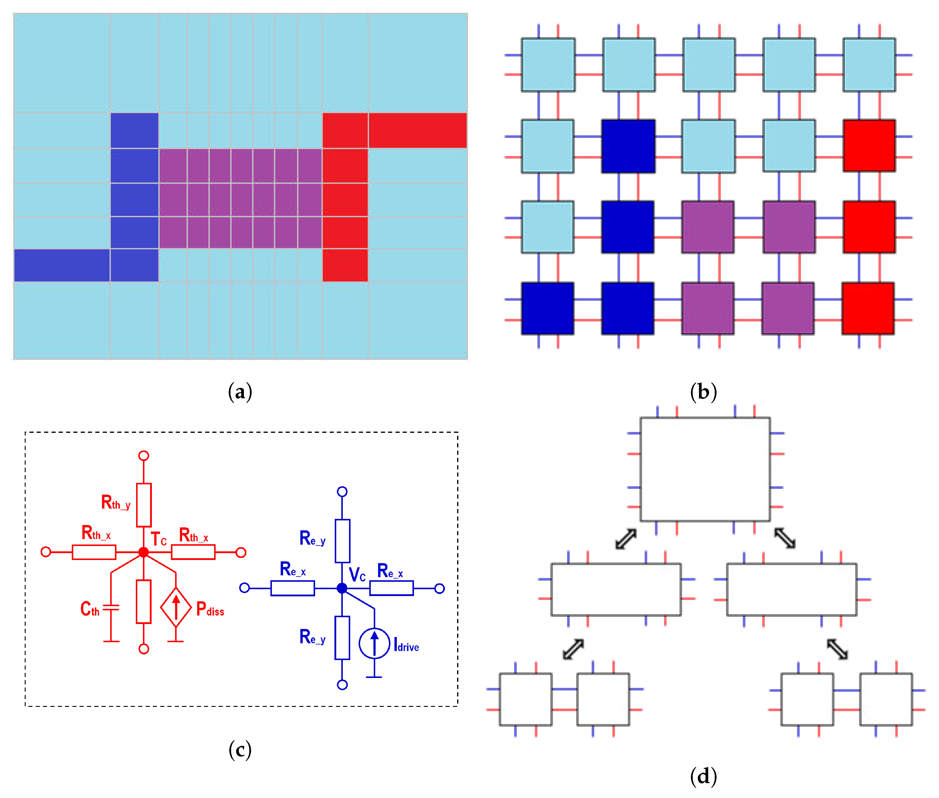
Figure 6.
Hysteresis model in the custom simulator.

Figure 7.
SUNRED model for VO2 vertical resistor.

Figure 8.
Excitation current per simulation step.

Figure 9.
V-I curve of VO2 vertical structures: (a) simulation example, r = 10 μm, h = 60 nm, and ambient temperature is 50 °C and (b) the general shape for all other simulations.
Figure 9.
V-I curve of VO2 vertical structures: (a) simulation example, r = 10 μm, h = 60 nm, and ambient temperature is 50 °C and (b) the general shape for all other simulations.

Figure 10.
V-I curve of (r = 10 μm, h = 50 nm) vertical VO2 resistor based on: (a) Laboratory measurement. (b) Simulation results.
Figure 10.
V-I curve of (r = 10 μm, h = 50 nm) vertical VO2 resistor based on: (a) Laboratory measurement. (b) Simulation results.
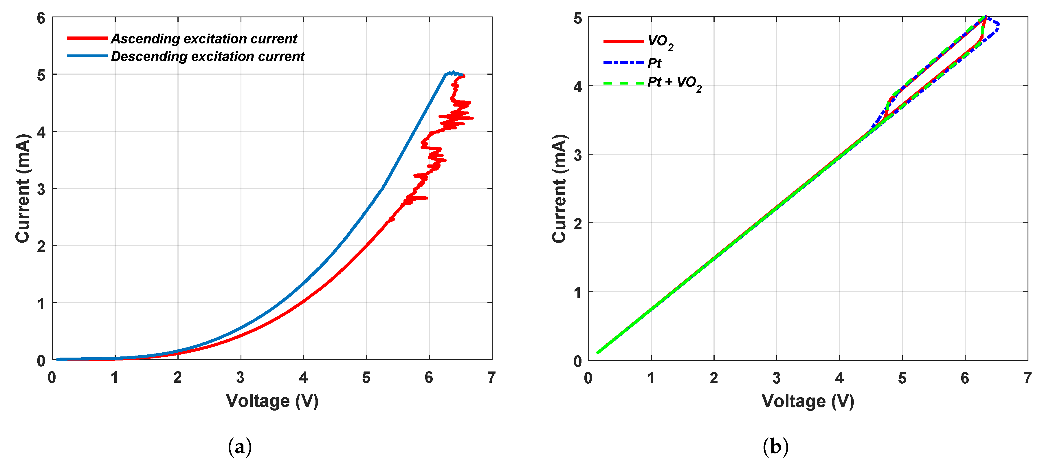
Figure 11.
VO2 resistance during (a) the nonconductive phase and (b) during the conductive phase at different thicknesses.
Figure 11.
VO2 resistance during (a) the nonconductive phase and (b) during the conductive phase at different thicknesses.

Figure 12.
The dependence of the (a) opening and (b) closing currents on the thickness of the VO2 resistor.
Figure 12.
The dependence of the (a) opening and (b) closing currents on the thickness of the VO2 resistor.

Figure 13.
VO2 resistance during (a) the nonconductive phase and (b) during the conductive phase at different radii.
Figure 13.
VO2 resistance during (a) the nonconductive phase and (b) during the conductive phase at different radii.
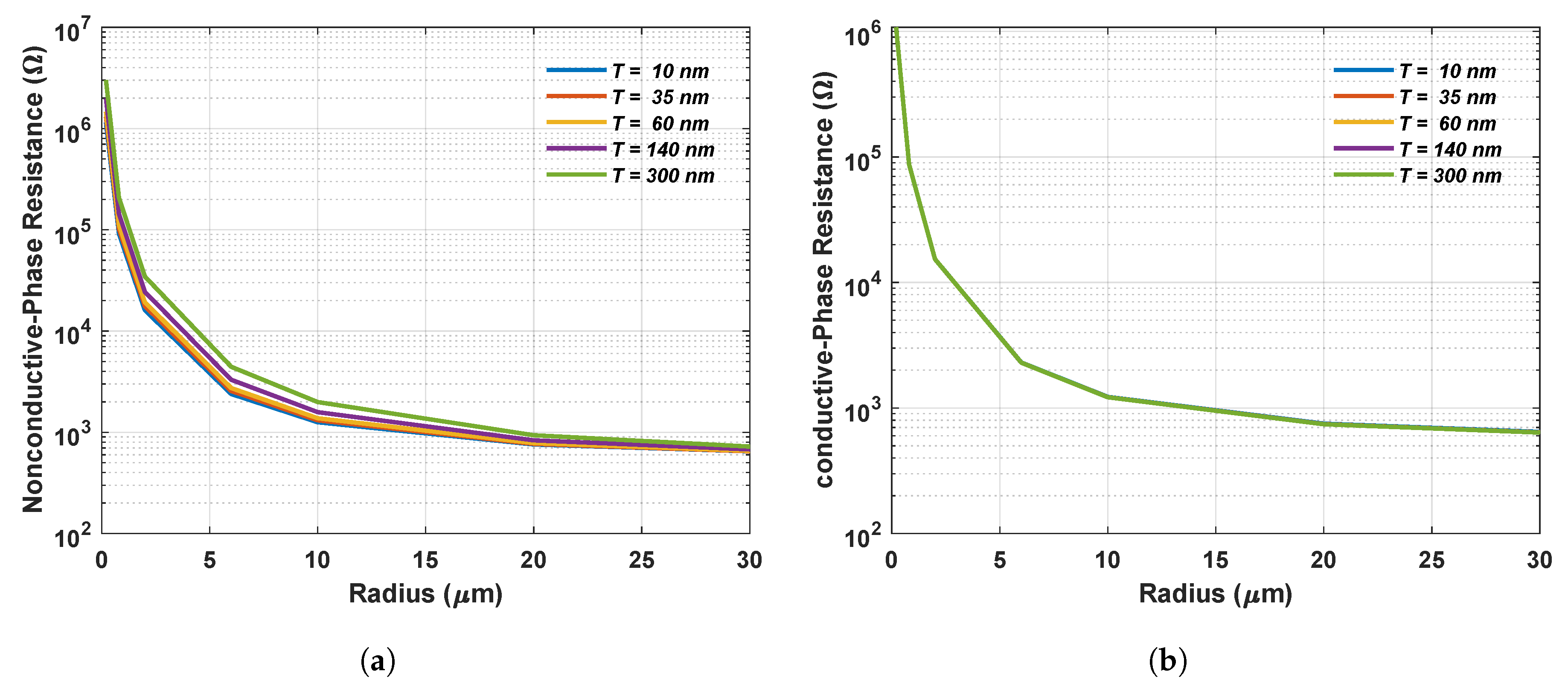
Figure 14.
The dependence of the (a) opening and (b) closing currents on the radius of the VO2 resistor.
Figure 14.
The dependence of the (a) opening and (b) closing currents on the radius of the VO2 resistor.

Figure 15.
The dependence of the maximum switching resistance on (a) the thickness and (b) the radius of the VO2 resistor.
Figure 15.
The dependence of the maximum switching resistance on (a) the thickness and (b) the radius of the VO2 resistor.
© 2020 by the authors. Licensee MDPI, Basel, Switzerland. This article is an open access article distributed under the terms and conditions of the Creative Commons Attribution (CC BY) license (http://creativecommons.org/licenses/by/4.0/).
Share and Cite
MDPI and ACS Style
Darwish, M.; Neumann, P.; Mizsei, J.; Pohl, L. Electro-Thermal Simulation of Vertical VO2 Thermal-Electronic Circuit Elements. Energies 2020, 13, 3447. https://doi.org/10.3390/en13133447
AMA Style
Darwish M, Neumann P, Mizsei J, Pohl L. Electro-Thermal Simulation of Vertical VO2 Thermal-Electronic Circuit Elements. Energies. 2020; 13(13):3447. https://doi.org/10.3390/en13133447
Chicago/Turabian StyleDarwish, Mahmoud, Péter Neumann, János Mizsei, and László Pohl. 2020. "Electro-Thermal Simulation of Vertical VO2 Thermal-Electronic Circuit Elements" Energies 13, no. 13: 3447. https://doi.org/10.3390/en13133447
Note that from the first issue of 2016, this journal uses article numbers instead of page numbers. See further details here.