Electro-Thermal Simulation of Vertical VO2 Thermal-Electronic Circuit Elements


Abstract
1. Introduction
- In a tunneling FET, conduction occurs through band-to-band tunneling. Gate voltage shifts the energy bands and changes the probabilities of tunneling [11].
- In a graphene pn-junction, transmission or a total internal reflection of electrons occurs by switching the electrostatic p and n doping of graphene by applying voltage to electrodes. The current routes to one or other output of the device [12].
- The bilayer pseudospin FET is an orbitronic device. Holes are injected into one monolayer of graphene and electrons into another monolayer and they may bind into excitons. The excitons may relax into a Bose–Einstein condensate (BEC) state. The current between source and drain first grows with the increase of voltage and then decreases as the carrier imbalance destroys BEC causing negative differential resistance [13].
- Spintronic devices are based on magnetic dipoles represented by electrons with polarized spins or ferromagnetic elements. Spintronic devices are nonvolatile (preserve the state when the power is turned off). Some possible types are as follows: The SpinFET combines a MOSFET and a switchable magnetic element [14]. The spin transfer domain wall device operates by the motion of a domain wall in a ferromagnetic wire [15]. The spintronic majority gate uses ferromagnetic wires and majority of the input currents’ directions sets the direction of magnetization [16]. In the all spin logic device, nanomagnets are placed over a copper wire and a diffusion spin current exerts a torque on a nanomagnet to switch its polarization [17].
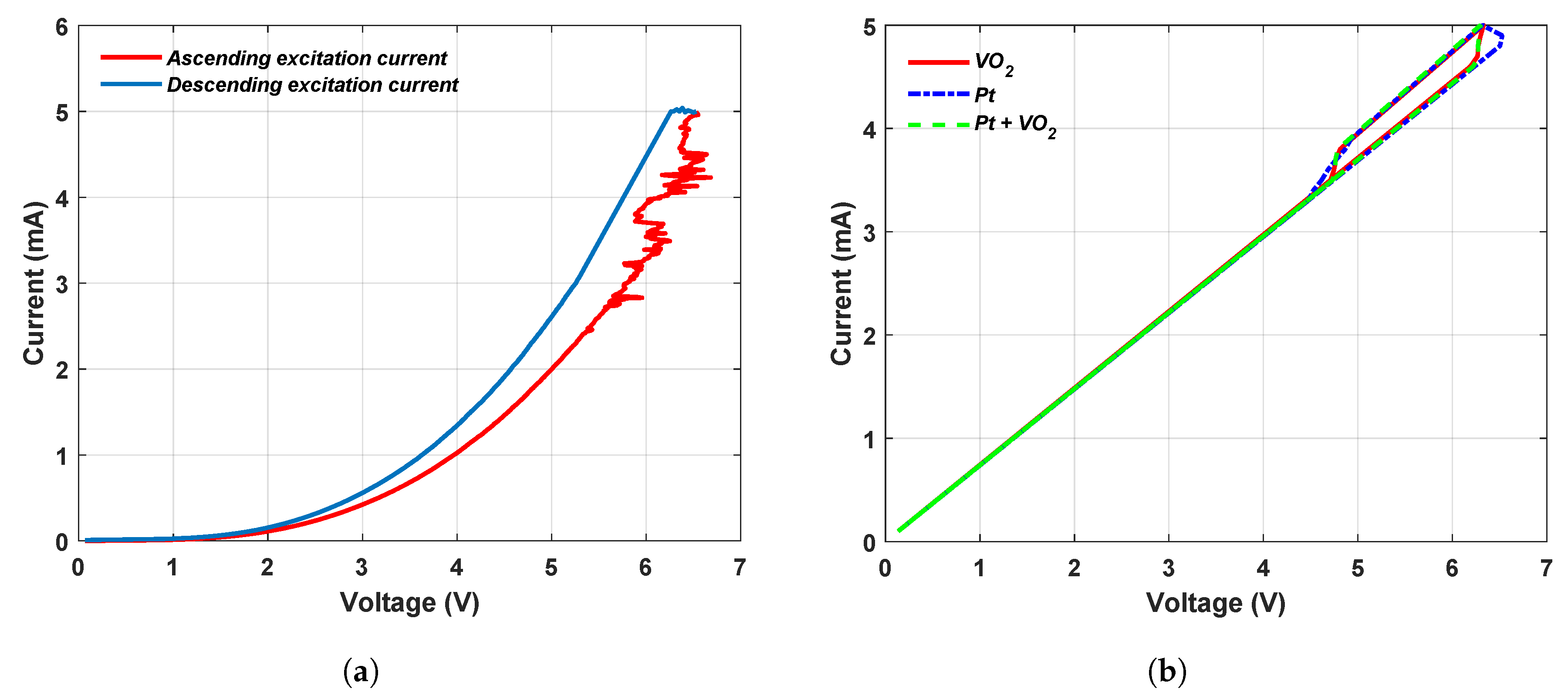
2. Experimentation
3. Electro-Thermal Simulation
3.1. Computational Method (SUNRED)
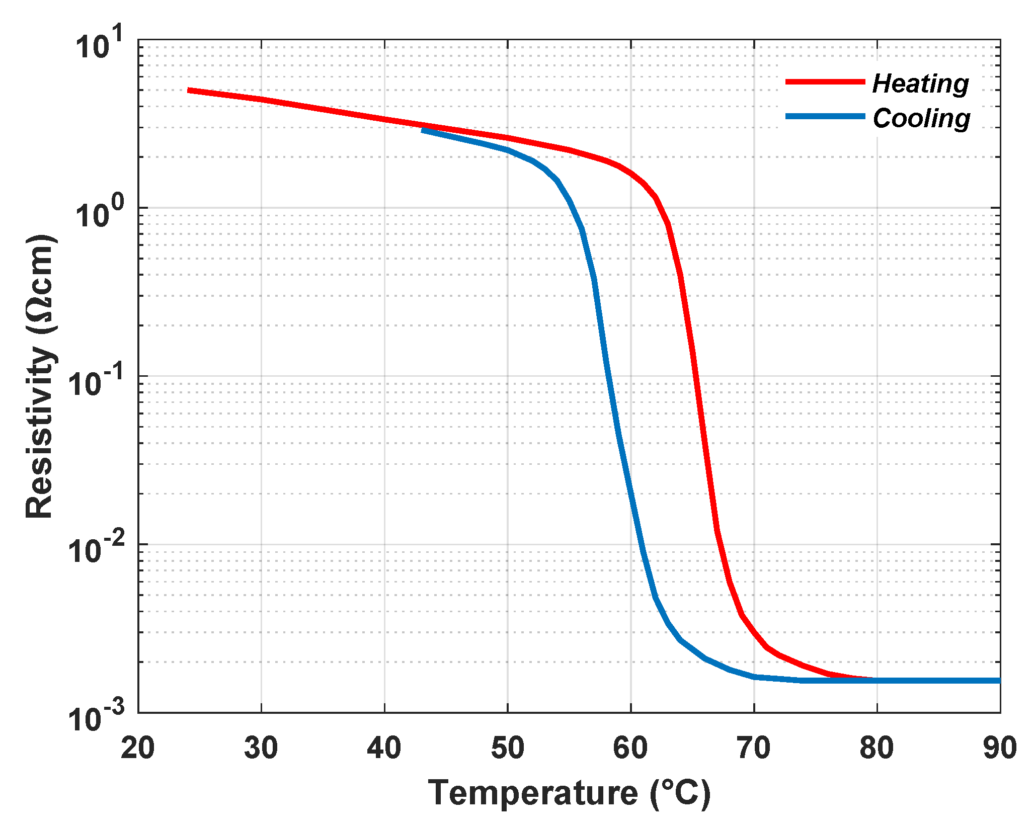
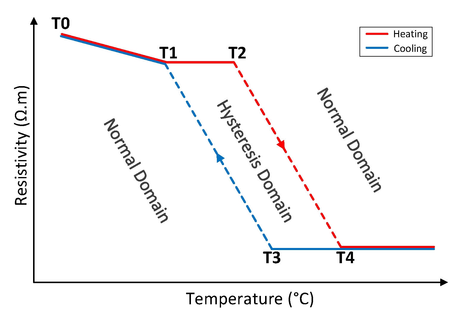
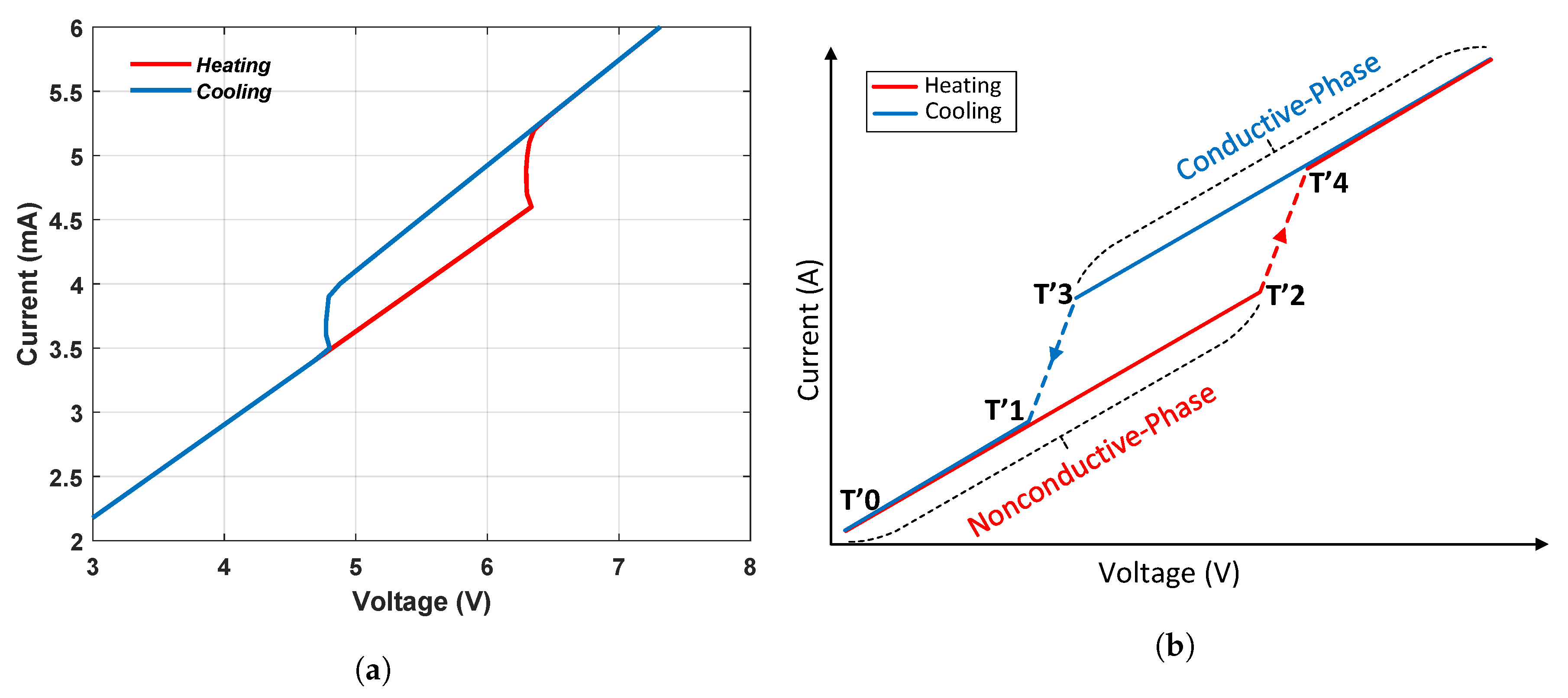
3.2. Hysteresis Model
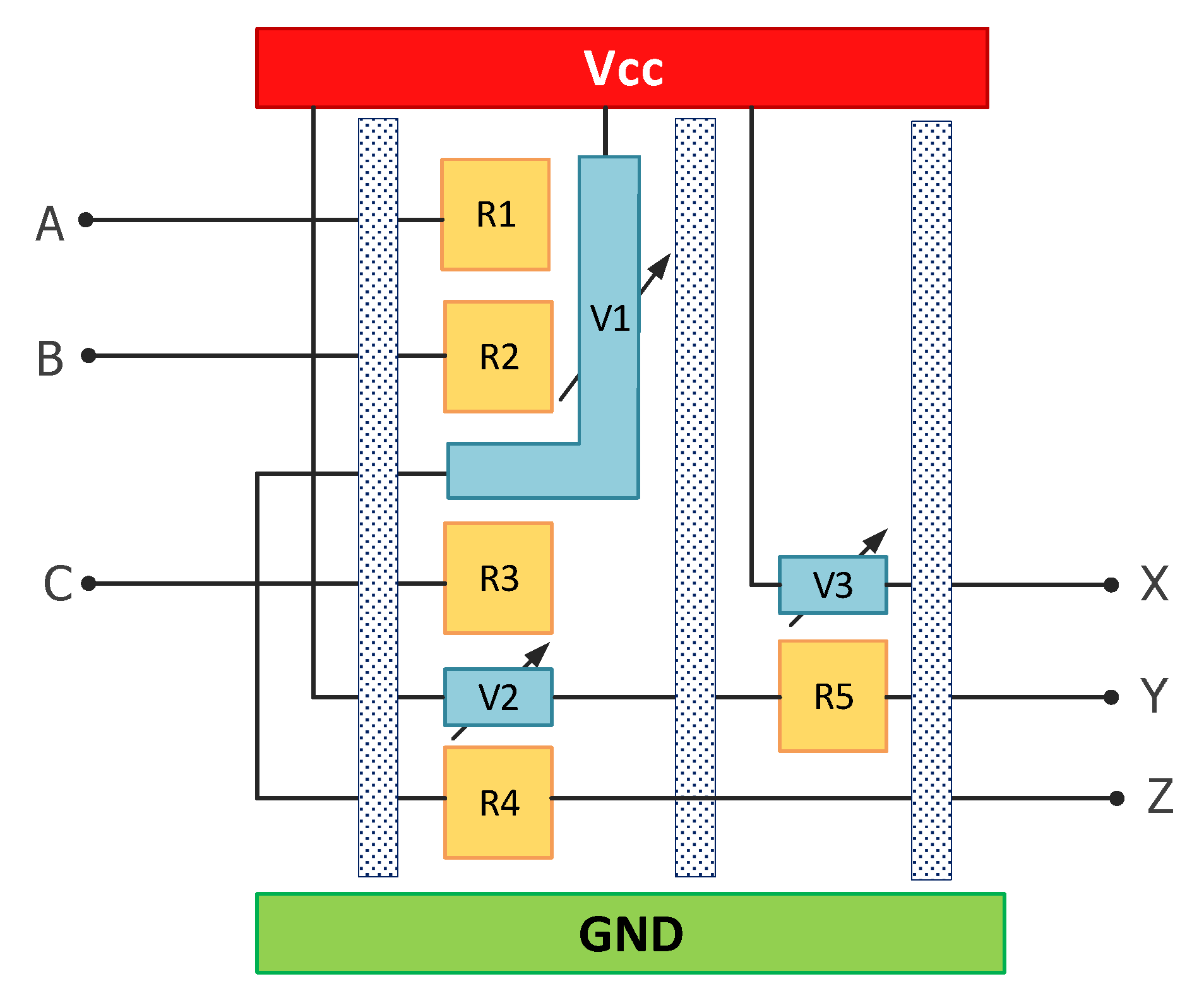
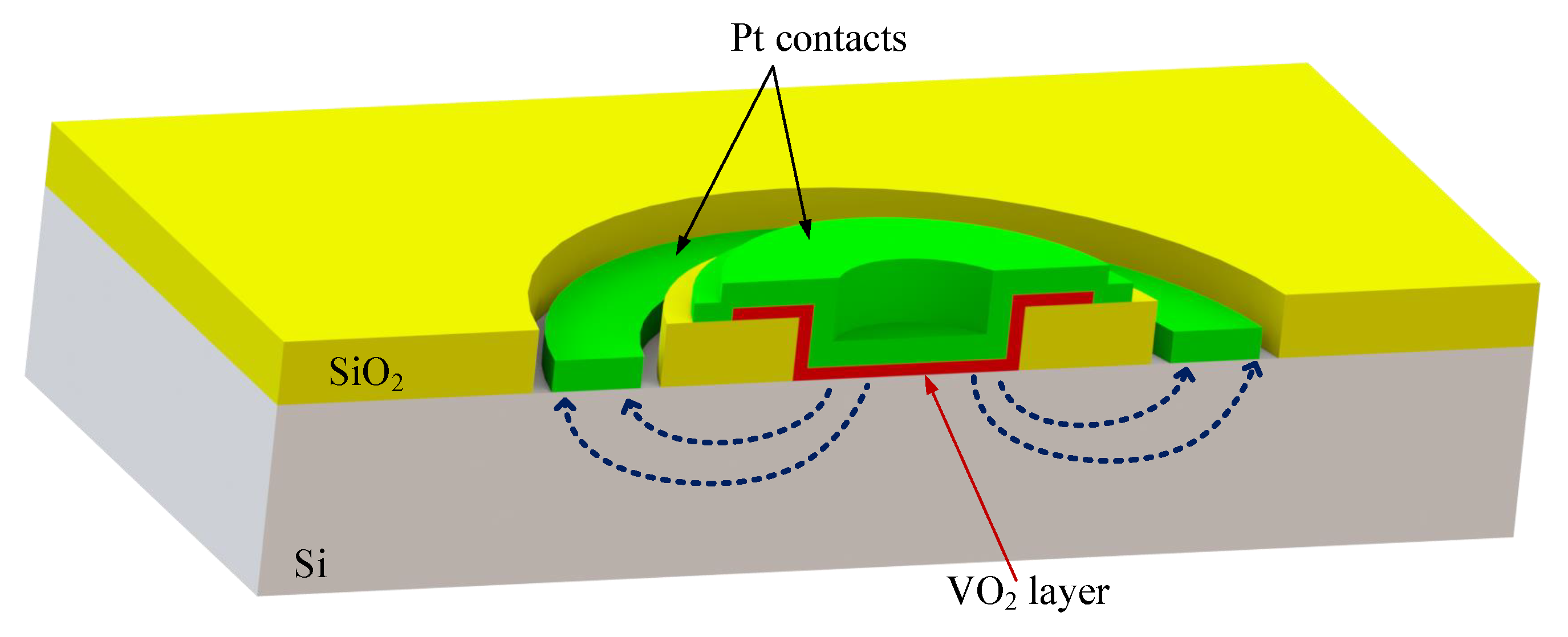
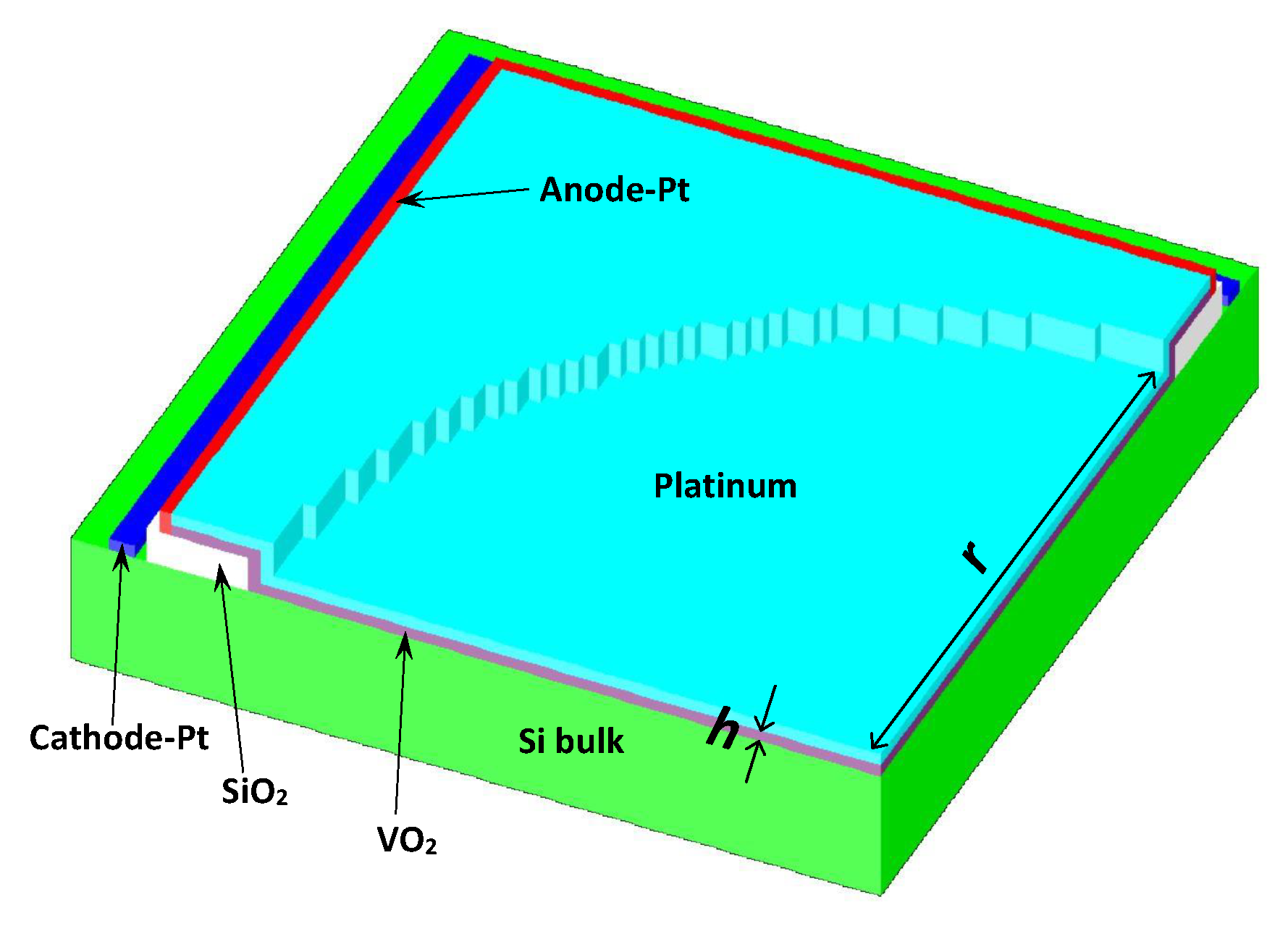
3.3. Geometry of the Simulated Structure
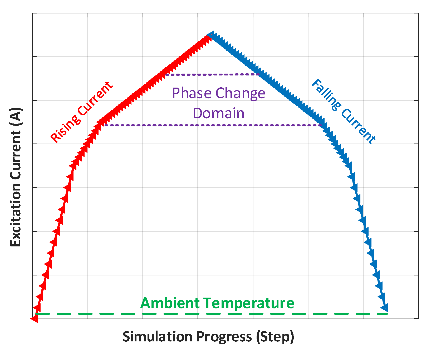
3.4. Excitation Required for the Simulation
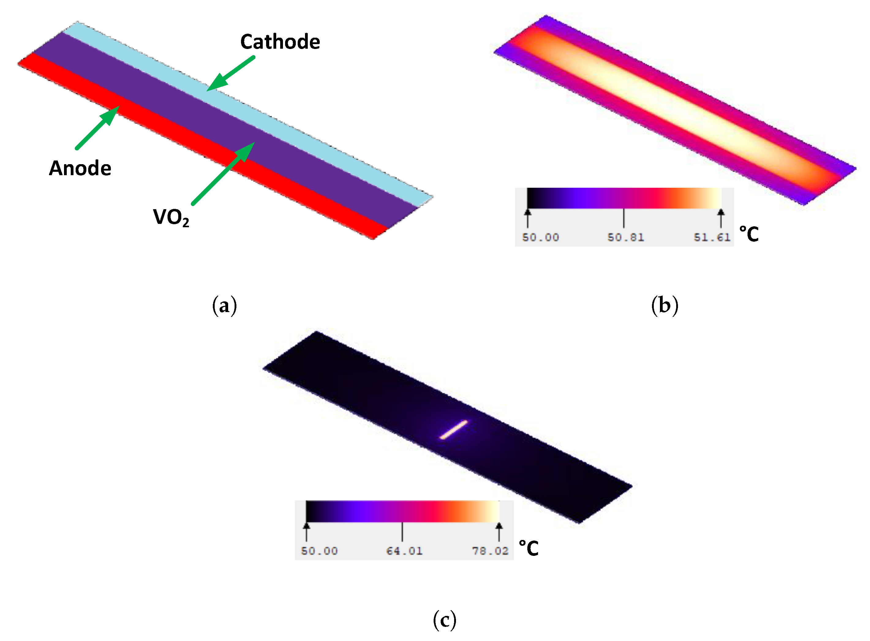
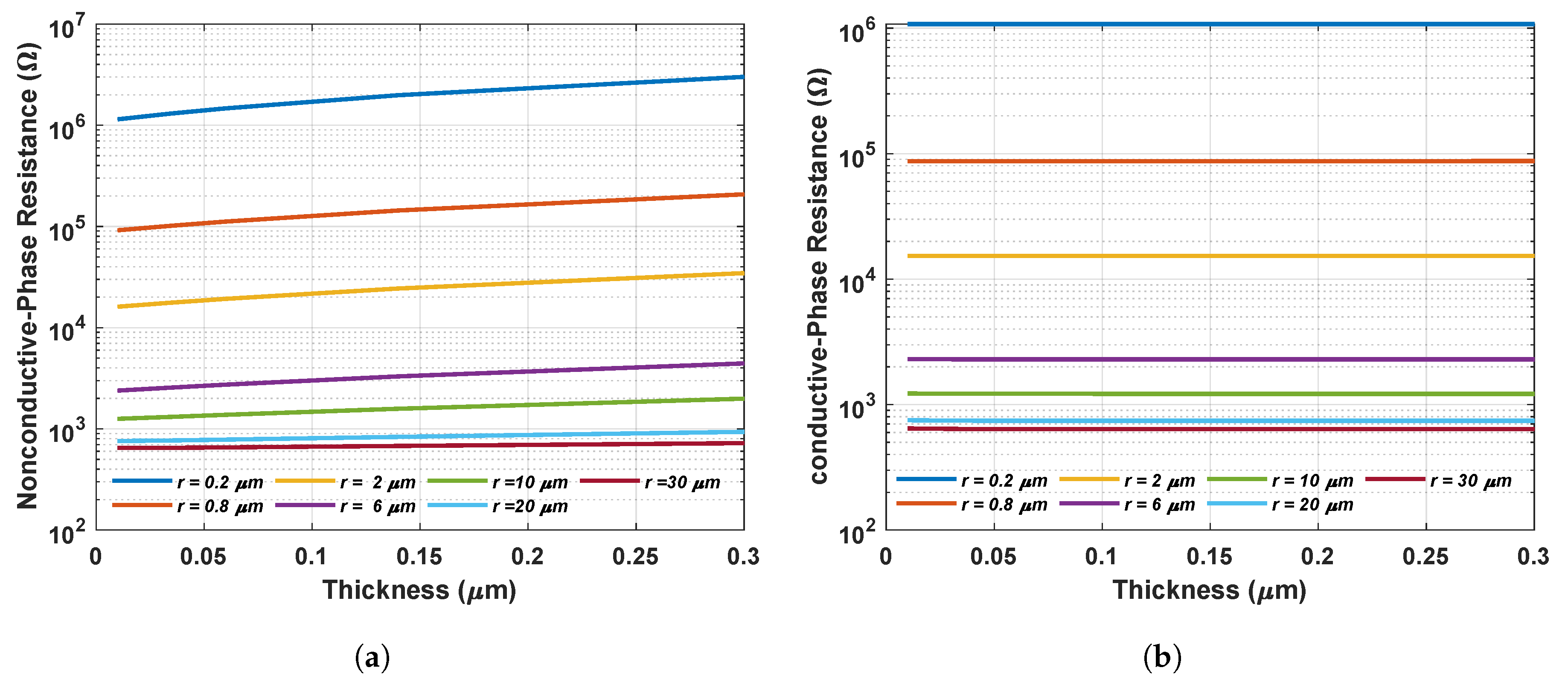
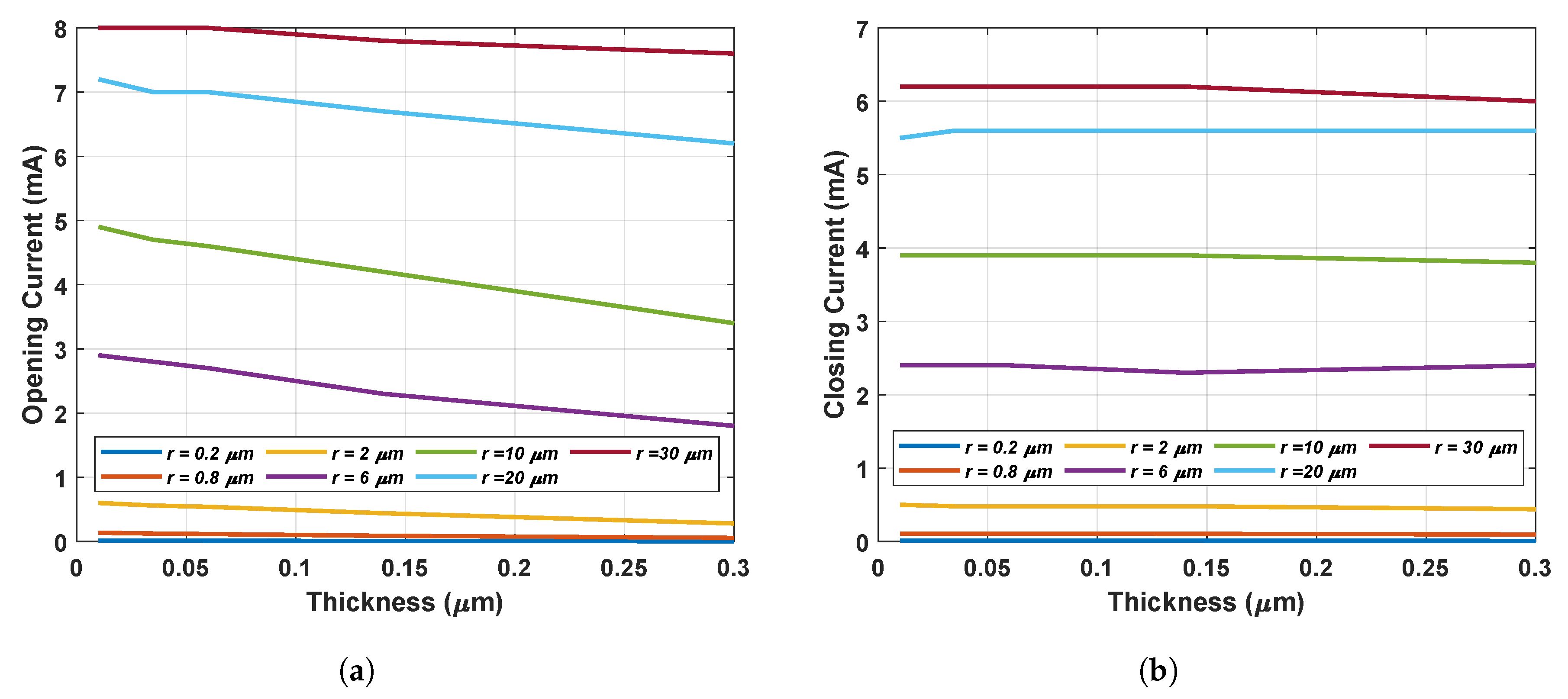
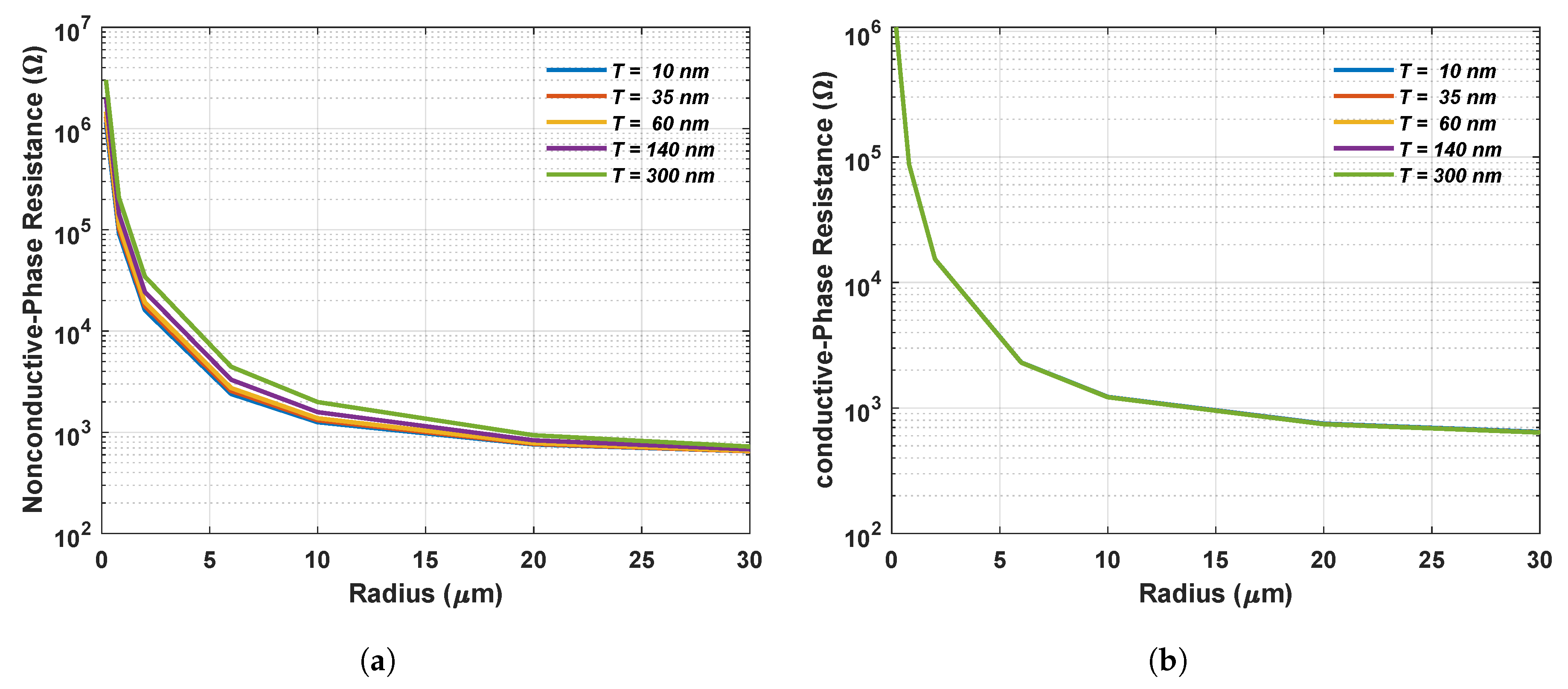
4. Results and Discussion
4.1. Dependence on Thickness
4.2. Dependence on Radius
5. Conclusions
Author Contributions
Funding
Conflicts of Interest
Abbreviations
| VO2 | Vanadium dioxide |
| CMOS | Complementary metal–oxide–semiconductor |
| TELC | Thermal-electronic logic circuits |
| SMT | Semiconductor-to-metal transition |
| Si | Silicon |
| SiO2 | Silicon dioxide |
| RF | Radio frequency |
| Pt | Platinum |
| FDM | Finite difference method |
| FEM | Finite element method |
| FVM | Finite volume method |
| HTC | Heat transfer coefficient |
| SUNRED | Successive network reduction method (also the simulator name) |
References
- Shalf, J. The future of computing beyond Moore’s Law. Philos. Trans. R. Soc. A Math. Phys. Eng. Sci. 2020, 378, 20190061. [Google Scholar] [CrossRef] [PubMed]
- Markov, I.L. Limits on fundamental limits to computation. Nature 2014, 512, 147–154. [Google Scholar] [CrossRef]
- Shalf, J.M.; Leland, R. Computing beyond Moore’s Law. Computer 2015, 48, 14–23. [Google Scholar] [CrossRef]
- Joneckis, L.; Koester, D.; Alspector, J. An Initial Look at Alternative Computing Technologies for the Intelligence Community; Technical Report; Institute for Defense Analyses: Alexandria, VA, USA, 2014. [Google Scholar]
- Thompson, N.; Spanuth, S. The Decline of Computers As a General Purpose Technology: Why Deep Learning and the End of Moore’s Law are Fragmenting Computing. SSRN Electron. J. 2018. [Google Scholar] [CrossRef]
- Jouppi, N.P.; Young, C.; Patil, N.; Patterson, D.; Agrawal, G.; Bajwa, R.; Bates, S.; Bhatia, S.; Boden, N.; Borchers, A.; et al. In-Datacenter Performance Analysis of a Tensor Processing Unit. In Proceedings of the 44th Annual International Symposium on Computer Architecture; ACM: New York, NY, USA, 2017; pp. 1–12. [Google Scholar] [CrossRef]
- Caulfield, A.M.; Chung, E.S.; Putnam, A.; Angepat, H.; Fowers, J.; Haselman, M.; Heil, S.; Humphrey, M.; Kaur, P.; Kim, J.Y.; et al. A cloud-scale acceleration architecture. In Proceedings of the 2016 49th Annual IEEE/ACM International Symposium on Microarchitecture (MICRO), Taipei, Taiwan, 15–19 October 2016; pp. 1–13. [Google Scholar] [CrossRef]
- Hill, M.D.; Reddi, V.J. Accelerator-level Parallelism. arXiv 2019, arXiv:1907.02064. [Google Scholar]
- Ingerly, D.B.; Enamul, K.; Gomes, W.; Jones, D.; Kolluru, K.C.; Kandas, A.; Kim, G.S.; Ma, H.; Pantuso, D.; Petersburg, C.; et al. Foveros: 3D Integration and the use of Face-to-Face Chip Stacking for Logic Devices. In Proceedings of the 2019 IEEE International Electron Devices Meeting (IEDM), San Francisco, CA, USA, 7–11 December 2019; pp. 19.6.1–19.6.4. [Google Scholar] [CrossRef]
- Nikonov, D.E.; Young, I.A. Overview of Beyond-CMOS Devices and a Uniform Methodology for Their Benchmarking. Proc. IEEE 2013, 101, 2498–2533. [Google Scholar] [CrossRef]
- Seabaugh, A.C.; Zhang, Q. Low-Voltage Tunnel Transistors for Beyond CMOS Logic. Proc. IEEE 2010, 98, 2095–2110. [Google Scholar] [CrossRef]
- Low, T.; Appenzeller, J. Electronic transport properties of a tilted graphene p-n junction. Phys. Rev. B 2009, 80, 155406. [Google Scholar] [CrossRef]
- Banerjee, S.; Register, L.; Tutuc, E.; Reddy, D.; MacDonald, A. Bilayer PseudoSpin Field-Effect Transistor (BiSFET): A Proposed New Logic Device. IEEE Electron Device Lett. 2009, 30, 158–160. [Google Scholar] [CrossRef]
- Sugahara, S.; Tanaka, M. A spin metal–oxide–semiconductor field-effect transistor using half-metallic-ferromagnet contacts for the source and drain. Appl. Phys. Lett. 2004, 84, 2307–2309. [Google Scholar] [CrossRef]
- Currivan, J.A.; Jang, Y.; Mascaro, M.D.; Baldo, M.A.; Ross, C.A. Low Energy Magnetic Domain Wall Logic in Short, Narrow, Ferromagnetic Wires. IEEE Magn. Lett. 2012, 3, 3000104. [Google Scholar] [CrossRef]
- Nikonov, D.E.; Bourianoff, G.I.; Ghani, T. Proposal of a Spin Torque Majority Gate Logic. IEEE Electron Device Lett. 2011, 32, 1128–1130. [Google Scholar] [CrossRef]
- Behin-Aein, B.; Datta, D.; Salahuddin, S.; Datta, S. Proposal for an all-spin logic device with built-in memory. Nat. Nanotechnol. 2010, 5, 266–270. [Google Scholar] [CrossRef]
- Mizsei, J.; Lappalainen, J.; Bein, M.C. Thermal-electronic integrated logic. In Proceedings of the 19th International Workshop on Thermal Investigations of ICs and Systems (THERMINIC), Berlin, Germany, 25–27 September 2013; pp. 128–134. [Google Scholar] [CrossRef]
- Zylbersztejn, A.; Mott, N.F. Metal-insulator transition in vanadium dioxide. Phys. Rev. B 1975, 11, 4383–4395. [Google Scholar] [CrossRef]
- Limelette, P. Universality and Critical Behavior at the Mott Transition. Science 2003, 302, 89–92. [Google Scholar] [CrossRef] [PubMed]
- Lappalainen, J.; Heinilehto, S.; Jantunen, H.; Lantto, V. Electrical and optical properties of metal-insulator-transition VO2 thin films. J. Electroceram. 2009, 22, 73–77. [Google Scholar] [CrossRef]
- Chain, E.E. Optical properties of vanadium dioxide and vanadium pentoxide thin films. Appl. Opt. 1991, 30, 2782. [Google Scholar] [CrossRef]
- Rozgonyi, G.A.; Hensler, D.H. Structural and Electrical Properties of Vanadium Dioxide Thin Films. J. Vac. Sci. Technol. 1968, 5, 194–199. [Google Scholar] [CrossRef]
- Budai, J.D.; Hong, J.; Manley, M.E.; Specht, E.D.; Li, C.W.; Tischler, J.Z.; Abernathy, D.L.; Said, A.H.; Leu, B.M.; Boatner, L.A.; et al. Metallization of vanadium dioxide driven by large phonon entropy. Nature 2014, 515, 535–539. [Google Scholar] [CrossRef]
- Qazilbash, M.M.; Brehm, M.; Chae, B.G.; Ho, P.C.; Andreev, G.O.; Kim, B.J.; Yun, S.J.; Balatsky, A.V.; Maple, M.B.; Keilmann, F.; et al. Mott Transition in VO2 Revealed by Infrared Spectroscopy and Nano-Imaging. Science 2007, 318, 1750–1753. [Google Scholar] [CrossRef]
- Kim, H.T.; Lee, Y.W.; Kim, B.J.; Chae, B.G.; Yun, S.J.; Kang, K.Y.; Han, K.J.; Yee, K.J.; Lim, Y.S. Monoclinic and correlated metal phase in VO2 as evidence of the Mott transition: Coherent phonon analysis. Phys. Rev. Lett. 2006, 97, 266401. [Google Scholar] [CrossRef]
- Gomez-Heredia, C.L.; Ramirez-Rincon, J.A.; Ordonez-Miranda, J.; Ares, O.; Alvarado-Gil, J.J.; Champeaux, C.; Dumas-Bouchiat, F.; Ezzahri, Y.; Joulain, K. Thermal hysteresis measurement of the VO2 emissivity and its application in thermal rectification. Sci. Rep. 2018, 8, 8479. [Google Scholar] [CrossRef]
- Hamaoui, G.; Horny, N.; Gomez-Heredia, C.L.; Ramirez-Rincon, J.A.; Ordonez-Miranda, J.; Champeaux, C.; Dumas-Bouchiat, F.; Alvarado-Gil, J.J.; Ezzahri, Y.; Joulain, K.; et al. Thermophysical characterisation of VO2 thin films hysteresis and its application in thermal rectification. Sci. Rep. 2019, 9, 8728. [Google Scholar] [CrossRef]
- Hu, B.; Zhang, Y.; Chen, W.; Xu, C.; Wang, Z.L. Self-heating and External Strain Coupling Induced Phase Transition of VO2 Nanobeam as Single Domain Switch. Adv. Mater. 2011, 23, 3536–3541. [Google Scholar] [CrossRef] [PubMed]
- Soltani, M.; Chaker, M.; Haddad, E.; Kruzelesky, R.V. Thermochromic vanadium dioxide smart coatings grown on Kapton substrates by reactive pulsed laser deposition. J. Vac. Sci. Technol. A Vac. Surf. Films 2006, 24, 612–617. [Google Scholar] [CrossRef]
- Datta, S.; Shukla, N.; Cotter, M.; Parihar, A.; Raychowdhury, A. Neuro Inspired Computing with Coupled Relaxation Oscillators. In Proceedings of the The 51st Annual Design Automation Conference on Design Automation Conference—DAC’14; ACM Press: New York, NY, USA, 2014; pp. 1–6. [Google Scholar] [CrossRef]
- Zhou, Y.; Ramanathan, S. Mott Memory and Neuromorphic Devices. Proc. IEEE 2015, 103, 1289–1310. [Google Scholar] [CrossRef]
- Ordonez-Miranda, J.; Ezzahri, Y.; Drevillon, J.; Joulain, K. Dynamical heat transport amplification in a far-field thermal transistor of VO2 excited with a laser of modulated intensity. J. Appl. Phys. 2016, 119, 203105. [Google Scholar] [CrossRef]
- Prod’Homme, H.; Ordonez-Miranda, J.; Ezzahri, Y.; Drevillon, J.; Joulain, K. VO2 -based radiative thermal transistor in the static regime 2017. arXiv 2017, arXiv:1710.10332. [Google Scholar]
- Chen, C.; Zhao, Y.; Pan, X.; Kuryatkov, V.; Bernussi, A.; Holtz, M.; Fan, Z. Influence of defects on structural and electrical properties of VO2 thin films. J. Appl. Phys. 2011, 110, 023707. [Google Scholar] [CrossRef]
- Jian, J.; Chen, A.; Zhang, W.; Wang, H. Sharp semiconductor-to-metal transition of VO2 thin films on glass substrates. J. Appl. Phys. 2013, 114, 244301. [Google Scholar] [CrossRef]
- Taha, M.; Walia, S.; Ahmed, T.; Headland, D.; Withayachumnankul, W.; Sriram, S.; Bhaskaran, M. Insulator—Metal transition in substrate-independent VO2 thin film for phase-change devices. Sci. Rep. 2017, 7, 17899. [Google Scholar] [CrossRef] [PubMed]
- Mizsei, J.; Bein, M.; Lappalainen, J.; Juhász, L.; Plesz, B. The Phonsistor—A Novel VO2 Based Nanoscale Thermal-electronic Device and Its Application in Thermal-electronic Logic Circuits (TELC). Mater. Today Proc. 2015, 2, 4272–4279. [Google Scholar] [CrossRef]
- Pohl, L.; Darwish, M.; Mizsei, J. Electro-Thermal Investigation of SMT Resistors for Thermal-Electrical Logic Circuits by Simulation. In Proceedings of the 2019 25th International Workshop on Thermal Investigations of ICs and Systems (THERMINIC), Lecco, Italy, 25–27 September 2019; pp. 1–4. [Google Scholar] [CrossRef]
- Mizsei, J.; Lappalainen, J. Microelectronics, Nanoelectronics: Step behind the red brick wall using the thermal domain. Mater. Today Proc. 2019, 7, 888–893. [Google Scholar] [CrossRef]
- Pohl, L.; Ur, S.; Mizsei, J. Thermoelectrical modelling and simulation of devices based on VO2. Microelectron. Reliab. 2017, 79, 387–394. [Google Scholar] [CrossRef]
- Gopalakrishnan, G.; Ruzmetov, D.; Ramanathan, S. On the triggering mechanism for the metal–insulator transition in thin film VO2 devices: Electric field versus thermal effects. J. Mater. Sci. 2009, 44, 5345–5353. [Google Scholar] [CrossRef]
- Kumar, S.; Pickett, M.D.; Strachan, J.P.; Gibson, G.; Nishi, Y.; Williams, R.S. Local Temperature Redistribution and Structural Transition During Joule-Heating-Driven Conductance Switching in VO2. Adv. Mater. 2013, 25, 6128–6132. [Google Scholar] [CrossRef]
- Nagy, G.; Horváth, P.; Pohl, L.; Poppe, A. Advancing the thermal stability of 3D ICs using logi-thermal simulation. Microelectron. J. 2015, 46, 1114–1120. [Google Scholar] [CrossRef]
- PV Lighthouse: Resistivity Calculator. Available online: https://www.pvlighthouse.com.au (accessed on 21 June 2020).
- Muta, H. Electrical Properties of Platinum-Silicon Contact Annealed in an H 2 Ambient. Jpn. J. Appl. Phys. 1978, 17, 1089–1098. [Google Scholar] [CrossRef]
- Martens, K.; Radu, I.P.; Mertens, S.; Shi, X.; Nyns, L.; Cosemans, S.; Favia, P.; Bender, H.; Conard, T.; Schaekers, M.; et al. The VO2 interface, the metal-insulator transition tunnel junction, and the metal-insulator transition switch On-Off resistance. J. Appl. Phys. 2012, 112, 124501. [Google Scholar] [CrossRef]
- Rao Popuri, S.; Artemenko, A.; Labrugere, C.; Miclau, M.; Villesuzanne, A.; Pollet, M. VO2 (A): Reinvestigation of crystal structure, phase transition and crystal growth mechanisms. J. Solid State Chem. 2014, 213, 79–86. [Google Scholar] [CrossRef]


© 2020 by the authors. Licensee MDPI, Basel, Switzerland. This article is an open access article distributed under the terms and conditions of the Creative Commons Attribution (CC BY) license (http://creativecommons.org/licenses/by/4.0/).
Share and Cite
Darwish, M.; Neumann, P.; Mizsei, J.; Pohl, L. Electro-Thermal Simulation of Vertical VO2 Thermal-Electronic Circuit Elements. Energies 2020, 13, 3447. https://doi.org/10.3390/en13133447
Darwish M, Neumann P, Mizsei J, Pohl L. Electro-Thermal Simulation of Vertical VO2 Thermal-Electronic Circuit Elements. Energies. 2020; 13(13):3447. https://doi.org/10.3390/en13133447
Chicago/Turabian StyleDarwish, Mahmoud, Péter Neumann, János Mizsei, and László Pohl. 2020. "Electro-Thermal Simulation of Vertical VO2 Thermal-Electronic Circuit Elements" Energies 13, no. 13: 3447. https://doi.org/10.3390/en13133447
APA StyleDarwish, M., Neumann, P., Mizsei, J., & Pohl, L. (2020). Electro-Thermal Simulation of Vertical VO2 Thermal-Electronic Circuit Elements. Energies, 13(13), 3447. https://doi.org/10.3390/en13133447