Abstract
This paper is concerned with the derivation of a one-cycle controller for driving a single-stage buck-boost DC-AC micro-inverter in grid-tied applications. The topology under study is based on a full-bridge switch arrangement with no unfolder circuit. The proposed micro-inverter attains a high gain by applying a multi-winding tapped inductor and, therefore, can operate at grid-level voltage without using a DC-DC step-up stage. To minimize the switching loss, the proposed inverter is operated in the discontinuous conduction mode. The operation principles of the proposed topology in the discontinuous conduction mode are discussed and analyzed. Based on the analysis, the one-cycle control law and modulator circuitry needed to control the proposed micro-inverter are developed. The feasibility of the proposed modulation scheme is verified by simulation.
1. Introduction
For many years, considerable research and development efforts were invested in the development of solar energy technologies. While some were focused on harvesting the solar thermal power [1,2], others were dedicated to photovoltaic (PV) power generation. The rapid progress of photovoltaic power generation systems has aroused much interest in micro-inverter technologies. Micro-inverters are designed to directly connect a single PV panel to the grid, attain maximum power point tracking (MPPT), provide a “plug-and-play” feature, and allow easy expansion of the PV array. Micro-inverters rely on high voltage step-up capability to boost the low PV panel voltage to the utility level.
A two-stage micro-inverters employ a high-gain DC-DC stage followed by a regular inverter. The two-stage configuration is quite popular due to its ease of implementation and control. A prominent advantage of the two-stage approach is the presence of a DC link. Placed in between the DC-DC and the DC-AC stage, the DC link capacitor helps to balance the DC and AC power flow. The high voltage DC link requires a relatively low capacitance, possibly a non-electrolytic one. However, the downside of the two-stage concept is the higher cost and lower efficiency.
A single-stage micro-inverter can combine the voltage step-up and inversion functions in one power stage. Such a concept allows for low component counts, low cost, and high efficiency compared with the traditional two-state solution. Therefore, much of the recent research was in the field of single-stage micro-inverters. As a result, a significant number of boost-derived single-stage inverters with high voltage step-up capability were developed [3,4,5]. However, the boost-derived inverters typically have a dead-time gap in the output current near the line voltage zero crossing and, thus, a lower power factor.
The buck-boost derived single-stage micro-inverter topologies, due to their voltage step-up/down capability, can sustain the output current throughout the line period and therefore attain a high-power factor. The recent literature reports on several buck-boost-derived single-stage inverters with reduced cost and improved performance. The buck-boost-derived single-stage inverters with four switches were proposed in [6,7,8,9]. Furthermore, the single-stage buck-boost topologies with only three switches were reported in [10,11]. However, the voltage gain of the aforementioned topologies is comparable to the traditional buck-boost converter. Other attempts to attain a higher gain, based on the buck-boost configuration, were also reported. A few selected topologies of high-gain single-stage buck-boost inverters are shown in Figure 1. The topology in [12] adopted a switched inductor to have a higher gain by the factor of over that of the conventional buck-boost converter. However, the proposed topology has four switches, eight diodes, and four inductors. The single-stage buck-boost inverters with tapped inductor were proposed in [13,14], which can have much higher voltage gain than the classic topologies, whereas the total switches count sum up to eight. A tapped-inductor-based single-stage buck-boost topology in [15,16] had five switches, while only one switch operated at a high frequency so as to minimize the switching loss.
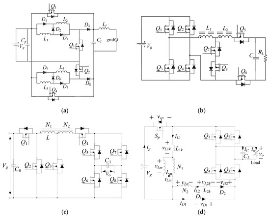
Figure 1.
Earlier high-gain single-stage buck-boost micro-inverters: (a) Reference [10]; (b) Reference [11]; (c) Reference [12]; (d) Reference [13,17].
The high switch count of the earlier counterparts, their topological complexity, and relatively high cost diminish the attractiveness of the single-stage inverters. Therefore, recently, additional efforts have been taken to develop an effective and affordable single-stage buck-boost micro-inverter topology.
Recently, a family of single-stage buck-boost micro-inverters was proposed in [17]. A prominent representative of this inverter family is illustrated in Figure 2. Hereafter, the topology in Figure 2 is referred to as the Single-Stage Buck-Boost Inverter (SSBBI). Initially, this earlier SSBBI version was successfully tested in the stand-alone application and was operated in the continuous conduction mode (CCM). SSBBI testing indicated the feasibility of the proposed scheme. However, most of the renewable energy systems are aimed at grid-tied applications. Therefore, this study is dedicated to the investigation of the challenges involved with the grid-tied operation of the SSBBI.
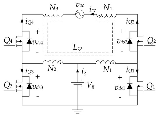
Figure 2.
The grid-tied single-stage buck-boost inverter (GT-SSBBI).
Switching losses caused by reverse recovery of the diodes is a major concern in inverter applications. One possible way to minimize the switching loss is to operate the power stage in the discontinuous conduction mode (DCM) to achieve zero-current turn-off and, thus minimize diodes’ reverse recovery. This calls for derivation of the appropriate controller suited for the DCM operational mode.
While a variety of control methods is available, here, the One-Cycle Control (OCC) approach is pursued. OCC is a nonlinear control strategy and pulse-width-modulation method applicable to switch-mode systems [18,19]. By controlling the duty cycle of the switches, OCC can enforce the average value of the switched variable to precisely follow the reference signal in each switching cycle. Therefore, OCC can reject the input source perturbation within a single cycle and with no application of a feedback loop. Furthermore, OCC has the merits of the constant switching frequency, fast dynamic response, and can attain a superior performance in power electronics applications.
For these reasons, OCC has received significant attention in the scientific community and has been widely used in practical industrial applications. OCC was applied in DC-DC switching converters [20,21], power factor corrector (PFC) rectifiers [22,23,24], and active power filters (APF) [25,26]. OCC was developed to meet the challenges of single and three-phase renewable energy applications such as grid-tied inverters (GTI) for photovoltaic (PV), fuel cells (FC), and wind power (WP) energy sources, together with the maximum power point tracking (MPPT) control [27,28]. OCC control schemes were also employed for uninterruptable power supplies (UPS), var generator, dynamic voltage restorer (DVR), electronic load, and motor control applications.
The objectives of this study were to develop the required OCC control law and, consequently, the OCC modulator circuitry needed for controlling the grid-tied SSBBI. The rest of the paper is organized as follows. The SSBBI is reviewed in Section 2. Section 3 introduces the operation principles of the SSBBI in the DCM regime. In Section 4, the derivation of the OCC law and the modulator implementation are presented. The design guide and example are given in Section 5. Section 6 reports the simulation results and, finally, concluding remarks are provided in Section 7.
2. SSBBI Review
The SSBBI topology in Figure 2 comprises a grounded source and a ground-referenced full-bridge. Here, the lower switches Q1 and Q3 are considered as primary devices, while the high switch pair Q2 and Q4 are operated as synchronous rectifiers. Furthermore, the body diodes of the high switches can be exploited as rectifiers. Hence, reverse recovery problems should be considered. To minimize the problem, DCM operation is attempted to provide zero-current switching and reduced switching loss.
The SSBBI makes use of a single multi-winding tapped inductor (TI). The TI is comprised of two symmetrical pairs of windings. The turns of the primary windings are N1 = N2. Similarly, equal secondary windings are used N3 = N4. The turn ratio of the tapped inductor is defined as n = N3/N1 = N4/N2.
In practice, an output filter capacitor, Co, is needed to reduce the switching ripple penetrating the grid. The voltage across Co is dictated by the AC line, vac. Better filtering of the high-frequency current components can be provided by a CLC type output filter (not considered in this paper).
Bipolar output current can be generated by SSBBI due to its symmetrical structure and symmetrical operation, and so can perform DC-AC inversion function. Properly chosen TI’s turn ratio, n, helps SSBBI to generate output current at grid level voltage when fed by a low DC voltage source. The desired output current can be controlled using any common control strategy, preferably at a constant frequency (for the ease of electro-magnetic interference (EMI) filtering). However, in this paper, the OCC modulation strategy is investigated.
The advantageous merits of the SSBBI are:
- Generating bipolar output current at grid level AC output voltage from a relatively low DC input voltage source without using an additional high-gain DC-DC stage;
- Low component count topology comprising a single magnetic device and four switches;
- The switches are assembled in a traditional full-bridge arrangement, suited for low-cost integrated-circuits drivers.
3. SSBBI Operation in the Discontinuous Conduction Mode
While operating in the DCM of the tapped inductor, the SSBBI has three switching states in each line half-cycle: states A, B, and C appear during the positive line half-cycle and the mirror (complementary) states A’, B’ and C’ during the negative line half-cycle.
The switching states of the SSBBI’s semiconductor switches are listed in Table 1, whereas the equivalent circuits of SSBBI’s states are illustrated in Figure 3.

Table 1.
Switching states of SSBBI’s semiconductor devices.
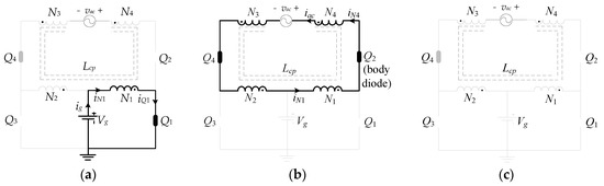
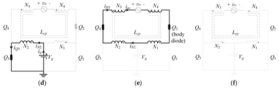
Figure 3.
Equivalent circuits (switching states) of the proposed SSBBI: (a) State A; (b) State B; (c) State C; (d) State A’; (e) State B’; (f) State C’.
The key theoretical waveforms of the SSBBI in the DCM mode are illustrated in Figure 4. Here, SQ1–SQ4 are the driving signals for the Q1–Q4 switches, respectively. Since the SSBBI operates symmetrically, only the positive half-cycle is analyzed. The primary winding of the tapped inductor is charged by the input source when Q1 is turned on and Q2 is turned off. Thus, the magnetizing current of the tapped inductor begins to ramp up. When Q1 is turned off, the energy stored in the taped inductor is discharged to the grid through all four of its windings. Hence, the magnetizing current of the tapped inductor is decreased from its peak to zero.
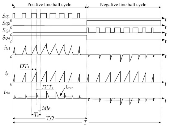
Figure 4.
Illustration of key waveforms of the proposed SSBBI.
In grid-tied applications, the task of the converter’s control circuit is to shape the average output current into a sinusoidal waveform (see iN4 in Figure 4). However, in stand-alone applications, the controller should regulate the output voltage.
4. Derivation of OCC Control Law
State A, see Figure 3a, appears at the beginning of each switching cycle in the positive line half-cycle. In this state, the switch Q1 is turned on for the duration of DTs, determined by the controller. Here, D is the ON duty cycle of the switch Q1 and Ts is the switching period. As a result, the TI’s magnetizing inductance, Lm, (referred to N1 winding) is charged by the DC input voltage source, Vg, and by the end of state A, reaches its peak current, Ipk, see Figure 5:
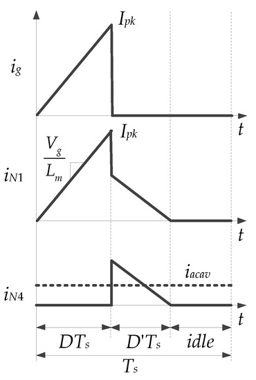
Figure 5.
Tapped inductor (TI) currents in discontinuous conduction mode (DCM) mode.
At this instant, the energy stored in the magnetizing inductance, Epk, is
State B, see Figure 3b, begins when the switch Q1 is turned off and lasts for the duration needed for the TI current to drop to zero. During this state, the energy stored in the tapped inductor is discharged into the grid. Therefore, the average power per switching cycle, Pav is
Here, fs = 1/Ts is the switching frequency.
State C, see Figure 3c is the DCM idle state. Here, none of the switches conduct and no energy flow occurs.
The average current per switching cycle, iacav(t), injected into the grid can be found from Equation (3) as:
The control goal of the grid-tied SSBBI is to fulfill the unity power factor constrain:
Here, Re is the emulated resistance of the inverter, assumed to be constant throughout the line cycle.
Combining Equations (4) and (5) implies
where the modulating voltage, Vm, is defined as
and ks, has the meaning of the line voltage sensor gain.
From Equation (7), the emulated resistance, Re, can be expressed as a linear function of the modulating voltage, Vm:
Therefore, the average power, PL, delivered by the GT-SSBBI to the grid throughout the line cycle is
Here, the power constant, kp, is defined as
Assuming that the modulating voltage, Vm, is a slowly varying signal, Equation (6) can be written applying the one-cycle control (OCC) technique as
where the integrator’s time constant is set equal to the switching period, Ti = Ts.
In fact, Equation (11) can be regarded as the desired OCC control law for the DCM GT-SSBBI. The block diagram of the required OCC modulator, which implements the control law Equation (11), is illustrated in Figure 6.
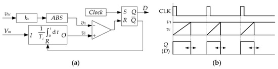
Figure 6.
One-cycle control (OCC) modulator for the DCM GT-SSBBI: (a) circuit implementation; (b) key waveforms.
The proposed OCC modulator in Figure 6 is a very simple circuit comprised of a resettable integrator, a comparator, a set/reset flip flop (SRFF) memory device, and a constant frequency clock. A line voltage sensor and an absolute value circuit are also needed.
It is worth noting that in photovoltaic applications the modulation voltage, Vm, is supposed to be provided for the OCC modulator by an external maximum power point tracker (MPPT) (not discussed in this paper).
5. Design Guidelines
5.1. Turn Ratio and Duty Cycle Constraints
During the state B (or B’), when the tapped inductor discharges the stored energy to the grid, the grid voltage is distributed across all four windings according to the turn ratio. Thus, an undesirable situation may arise if the voltage across the N2 (or N1) winding tends to be higher than the value of the DC source voltage, Vg. In such a case, the stored energy will be recycled back to the DC source (via the antiparallel diode of one of the lower switches) instead of being transferred to the grid. Therefore, for the proper operation of the SSBBI, the voltage across the primary windings must always be lower than the DC input voltage, Vg. The worth case occurs at the peak of the line:
Hence, the design constrain on TI’s turn ratio should be observed:
The volt-sec balance of the TI’s magnetizing inductance (referred to the N1 winding) states that
since in the DCM mode
and, since the maximum duty ratio, Dmax, occurs at the peak of the line, Equations (14) and (15) imply that to sustain the DCM, the duty-cycle, Dmax, generated by the controller should be constrained by
5.2. Design Procedure
The design procedure of the OCC GT-SSBBI is required to establish the parameters of the tapped inductor: the turn ratio, n, and the magnetizing inductance, Lm; and the parameters of the controller circuit: the sensor gain constant, ks, and the integrator’s gain constant, Ti. The parameters given are the effective line voltage, Vrms; the input source DC voltage, Vg; and the inverter’s full rated power, PL max. The procedure unfolds as follows:
- (1)
- Choose an acceptable switching frequency, fs;
- (2)
- Choose the turn ratio, n, to satisfy Equation (13);
- (3)
- Calculate the maximum duty cycle, Dmax, according to Equation (16). Considering parameter variations and possible transients, allow the practical maximum duty cycle to assume a somewhat smaller value of Dpk = 0.85 × Dmax;
- (4)
- According to Equation (9), the average power injected into the grid is inversely proportional to the square of the modulation voltage. Thus, to generate the full rated power, PL max, the modulation voltage has to assume its minimum value, Vm min. Hence, choose an acceptable value of the modulation voltage, Vm min, that suites the dynamic range of the controller’s circuitry signal;
- (5)
- The theoretical gain of the line sensor can be derived applying the full power and the peak of the line conditions as well as using Dpk for the maximum duty cycle to Equation (6):
- (6)
- The magnetizing inductance can be obtained from Equation (9) so to satisfy the rated power requirements
- (7)
- In practice, the output voltage of the line sensor should not exceed the maximum allowed input voltage, Vin max comp, of the OCC comparator, nor can it be too small a value. To exploit the entire dynamic range of comparator’s input, the practical value of the line voltage sensor gain, ks’, can be selected according to
- (8)
- Finally, to correctly implement the OCC control law Equation (11), the integrator’s time constant is adjusted considering the ratio of the theoretically required ks, see Equation (17), and the practical ks’, set according to (19):
The tuned OCC control scheme is shown in Figure 7, which also shows the line polarity detection and steering logic needed to distribute the driving signals to the power switches.
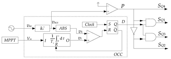
Figure 7.
Improved OCC modulator for the DCM GT-SSBBI.
5.3. Design Example
Design OCC GT-SSBBI micro-inverter to deliver PL max = 100 W into the Vrms = 110 V line when fed by a Vg = 48 V input source. The suggested design procedure is applied as follows.
- (1)
- The switching frequency of fs = 50 kHz is chosen;
- (2)
- The turn ratio according to Equation (13) is constrained by n > 0.62. Here, n = 1 is recommended;
- (3)
- The maximum duty cycle according to Equation (16) is Dmax = 0.447. Here, a more conservative value of Dpk = 0.38 is chosen;
- (4)
- By designer’s choice, Vm min = 0.5 at full power;
- (5)
- The required gain of the line sensor can be obtained using Equation (17) as ks = 0.0012;
- (6)
- The magnetizing inductance can be found, see Equation (18), as Lm = 16 μH;
- (7)
- By designer’s choice Vin max comp = 3 V and applying Equation (19), the practical gain of the line sensor is obtained as ks’ = 0.02;
- (8)
- Using Equation (20), the integrator’s time constant can be found as Ti = 1.2 × 10⁻⁶ s.
Based on the design example, the calculated emulated resistance is Re = 120.6 Ω, and average output power, PL = 100.3 W.
The theoretical expectations were verified by simulation.
The comparison plots of the calculated vs. the simulated results of output power, PL, and emulated resistance, Re and operating maximum duty cycle, Dpk, are shown in Figure 8. As can be seen from the plots, the calculated results are consistent with the simulated results, which again proves the accuracy of the design results.
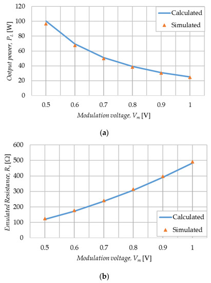
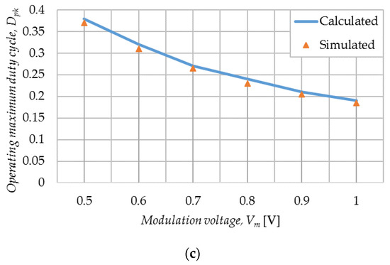
Figure 8.
Comparison of the calculated and the simulated results as a function of the modulating voltage, Vm: (a) the output power, PL; (b) the emulated resistance, Re; (c) the operating maximum duty cycle, Dpk.
6. Simulated Results of OCC Controlled DCM GT-SSBBI
To verify the feasibility of the proposed OCC GT-SSBBI, simulations were carried out by the PSIM v. 9.1 simulation software. The key simulation parameters of GT-SSBBI were: output power Po = 100 W; input voltage Vg = 48 V; line voltage Vac = 110 V/60 Hz; switching frequency fs = 50 kHz; magnetizing inductance of the tapped inductor Lm = 16 μH; turn ratio n = 1. The parameters of OCC controller were: line voltage sensor gain ks’ = 0.02; modulator voltage Vm = 0.5; integrator time constant Ti = 1.2 × 10⁻⁶ s.
The key waveforms of the OCC controller are shown in Figure 9.
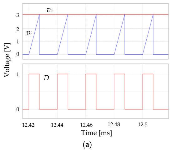
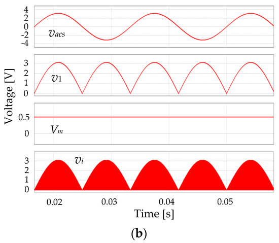
Figure 9.
Key waveforms of the OCC controller: (a) on switching period scale; (b) on the line period scale.
Figure 9a illustrates the generation of the duty cycle, D, by the OCC technique. Here, D assumes “high” at the beginning of each switching cycle and is set to “low” when the integrator output, vi, equals the reference signal of v1. Evidently, the duty cycle is generated properly.
The top trace in Figure 9b is the output of the line voltage sensor, vacs; the second trace is the rectified output of the sensed line voltage used as OCC reference signal, v1 = |vacs|. The bottom trace shows the OCC integrator’s output, vi, where the peak follows the rectified sinusoidal waveform and, thus, has the same outline as v1.
Key simulation results of OCC controlled GT-SSBBI at 100 W output power level are shown in Figure 10. Examining the waveforms reveals that the GT-SSBBI stands up to the theoretical expectations and generates the desired sinusoidal average output current at unity power factor. The parasitic parameters of the active and passive components were not considered, as the simulation was aimed at verification of the proposed OCC control scheme. Since the step-by-step simulation is generally accepted to be quite accurate tool, this provides confidence in the proposed topology and the OCC approach derived above.
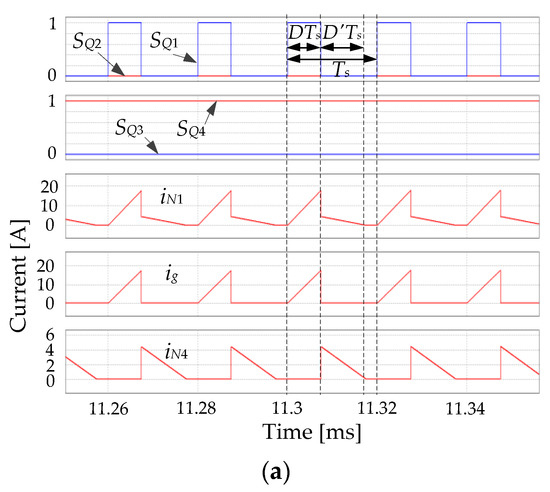
Figure 10.
Key simulation waveforms of the proposed OCC controlled GT-SSBBI: (a) driving signal and currents on the switching period scale; (b) Vds of the switches in one leg, output current, iac, line voltage, vac and average output current, iacav; (c) switch currents on the line period scale.
As it can be observed in Figure 10a, the simulation results are in close agreement with the analytical key waveforms in Figure 4. The idle period is visible at the end of each switching period, which proves the DCM operation of proposed GT-SSBBI. Furthermore, the line voltage and average output current of the proposed GT-SSBBI is given in Figure 10b, as well as the voltage across the switches in one leg. It can be observed in Figure 10b that the OCC-controlled GT-SSBBI can produce high-quality sinusoidal output current with the unity power factor. The currents flowing through the switches are presented in Figure 10c.
7. Conclusions
This paper introduced an OCC-controlled grid-tied single-stage buck-boost inverter. The proposed SSBBI topology is very simple and is comprised of a H-bridge switching structure and a single four-winding tapped inductor. Therefore, SSBBI can attain high voltage gain required in PV energy generation systems applications, while keeping a lower component count.
The paper described the SSBBI’s operation in DCM mode as a grid-tied inverter. The one-cycle control algorithm to operate the SSBBI in grid-tied operation was derived. Based on the theoretical derivations, the OCC modulator needed to control the SSBBI stage was developed. Design procedure for engineering design of the power stage and the associated control circuitry was also developed.
A grid-tied SSBBI was designed and verified by simulation. The reported simulation results stand in accord with the theoretical expectations. The simulation results are encouraging, having shown that the SSBBI topology is capable of delivering a well-shaped sinusoidal average current into the grid. Therefore, the SSBBI seems a feasible solution to single-stage micro-inverter applications.
Author Contributions
Conceptualization, A.A.; methodology, A.A. and B.Z.; software, B.Z.; validation, B.Z. and Y.H.; formal analysis, A.A.; investigation, A.A.; resources, Y.H.; writing—Original draft preparation, A.A.; writing—Review and editing, A.A. and B.Z.; visualization, Y.H.; supervision, A.A.; project administration, B.Z.; funding acquisition, B.Z. All authors have read and agreed to the published version of the manuscript.
Funding
This research was funded by the National Natural Science Foundation of China under Grant No. 51807164 and by Shaanxi Key R&D Program under Grant No. 2018GY-073 and by Xi’an Science and Technology Association Youth Talent Support Project.
Conflicts of Interest
The authors declare no conflict of interest.
Nomenclature and Abbreviations
| Q1, Q2, Q3, Q4, Q5 | the power switches |
| N1, N2, N3, N4 | the tapped-inductor windings |
| n | the turn ratio of the tapped-inductor |
| Co | output filter capacitor |
| vac | the AC line voltage |
| iac | the output/line current |
| iN1, iN2, iN3, iN4 | the currents through the windings |
| Vg | the input voltage |
| ig | the input current |
| iQ1, iQ3 | the currents through the switches Q1, Q3 |
| Lcp | the tapped-inductor |
| SQ1, SQ2, SQ3, SQ4 | the driving signals of the switches Q1~Q4 |
| D | the ON duty cycle |
| D’ | the OFF duty cycle |
| Ts | the switching period |
| T | the line period |
| iacav | the average output current |
| Lm | the tapped-inductor magnetizing inductance |
| Ipk | the peak inductor current |
| Epk | the peak energy stored in the magnetizing inductance |
| Pav | the average power per switching cycle |
| fs | the switching frequency |
| iacav(t) | the average current per switching cycle |
| Re | the emulated resistance of the inverter |
| Vm | the modulating voltage |
| ks | the line voltage sensor gain |
| PL | the average power delivered to the grid throughout the line cycle |
| kp | the power constant |
| Ti | the integrator’s time constant |
| Vrms | the root-mean-square value of output voltage |
| Dmax | the maximum ON duty cycle ratio |
| PL max | the inverter’s full rated power |
| Dpk | the practical maximum duty cycle |
| Vm min | the minimum value of the modulation voltage |
| Vin max comp | the maximum allowed input voltage of the OCC comparator |
| ks’ | the practical line voltage sensor gain |
| Po | the output power |
| vi | the integrator output signal of the OCC controller |
| v1 | the reference signal of the OCC controller |
| vacs | the output signal of the line voltage sensor |
| vds1, vds2 | voltage stress across the switches Q1, Q2 |
| PV | photovoltaic |
| MPPT | maximum power point tracking |
| SSBBI | single-stage buck-boost inverter |
| CCM | continuous conduction mode |
| GT-SSBBI | grid-tied single-stage buck-boost inverter |
| DCM | discontinuous conduction mode |
| OCC | one-cycle control |
| PFC | power factor corrector |
| APF | active power filters |
| GTI | grid-tied inverters |
| FC | fuel cells |
| WP | wind power |
| UPS | uninterruptable power supplies |
| DVR | dynamic voltage restorer |
| TI | tapped inductor |
| EMI | electro-magnetic interference |
| SRFF | set/reset flip flop |
References
- Rashid, K.; Safdarnejad, S.M.; Powell, K.M. Process intensification of solar thermal power using hybridization, flexible heat integration, and real-time optimization. Chem. Eng. Process.-Process. Intensif. 2019, 139, 155–171. [Google Scholar] [CrossRef]
- Alva, G.; Liu, L.; Huang, X.; Fang, G. Thermal energy storage materials and systems for solar energy applications. Renewable Sustainable Energy Rev. 2017, 68 pt 1, 693–706. [Google Scholar] [CrossRef]
- Meneses, D.; Blaabjerg, F.; Garcia, O.; Cobos, J.A. Review and comparison of step-up transformerless topologies for photovoltaic AC-module application. IEEE Trans. Power Electron. 2013, 28, 2649–2663. [Google Scholar] [CrossRef]
- Fang, Y.; Ma, X. A novel PV microinverter with coupled inductors and double-boost topology. IEEE Trans. Power Electron. 2010, 25, 3139–3147. [Google Scholar] [CrossRef]
- Abramovitz, A.; Zhao, B.; Smedley, K.M. High-gain single-stage boosting inverter for photovoltaic applications. IEEE Trans. Power Electron. 2016, 31, 3550–3558. [Google Scholar] [CrossRef]
- Kumar, A.; Gautam, V.; Sensarma, P. A SEPIC derived single-stage buck-boost inverter for photovoltaic applications. In Proceedings of the 2014 IEEE International Conference on Industrial Technology (ICIT), Busan, South Korea, 26 February–1 March 2014. [Google Scholar]
- Kumar, A.; Sensarma, P. A four-switch single-stage single-phase buck-boost inverter. IEEE Trans. Power Electron. 2017, 32, 5282–5292. [Google Scholar] [CrossRef]
- Kumar, A.; Sensarma, P. New switching strategy for single-mode operation of a single-stage buck-boost inverter. IEEE Trans. Power Electron. 2018, 33, 5927–5936. [Google Scholar] [CrossRef]
- Akbar, F.; Cha, H.; Lee, S.; Nguyen, T. A single-phase transformerless buck-boost inverter for standalone and grid-tied applications with reduced magnetic volume. In Proceedings of the 2019 10th International Conference on Power Electronics and ECCE Asia (ICPE 2019-ECCE Asia), Busan, South Korea, 27–30 May 2019. [Google Scholar]
- Zhang, Y.; Woldegiorgis, A.T.; Chang, L. Design and test of a novel buck-boost inverter with three switching devices. In Proceedings of the 2012 Twenty-Seventh Annual IEEE Applied Power Electronics Conference and Exposition (APEC), Orlando, FL, USA, 5–9 February 2012. [Google Scholar]
- Chowdhury, A.S.K.; Chakraborty, S.; Salam, K.M.A.; Razzak, M.A. Design of a single-stage grid-connected buck-boost photovoltaic inverter for residential application. In Proceedings of the 2014 Power and Energy Systems: Towards Sustainable Energy, Bangalore, India, 13–15 March 2014. [Google Scholar]
- Abdel-Rahim, O.; Orabi, M.; Ahmed, M.E. Buck-boost interleaved inverter for a grid-connected photovoltaic system. In Proceedings of the 2010 IEEE International Conference on Power and Energy, Kuala Lumpur, Malaysia, 29 November–1 December 2010. [Google Scholar]
- Tang, Y.; He, Y.; Dong, X. Active buck-boost inverter with coupled inductors. In Proceedings of the 2014 IEEE Energy Conversion Congress and Exposition (ECCE), Pittsburgh, PA, USA, 14–18 September 2014. [Google Scholar]
- Husev, O.; Matiushkin, O.; Roncero-Clemente, C.; Blaabjerg, F.; Vinnikov, D. Novel family of single-stage buck-boost inverters on the unfolding circuit. IEEE Trans. Power Electron. 2019, 34, 7662–7676. [Google Scholar] [CrossRef]
- Sreekanth, T.; Lakshminarasamma, N.; Mishra, M.K. Coupled inductor-based single-stage high gain DC-AC buck-boost inverter. IET Power Electron. 2016, 9, 1590–1599. [Google Scholar] [CrossRef]
- Sreekanth, T.; Lakshminarasamma, N.; Mishra, M.K. A single-stage grid-connected high gain buck-boost inverter with maximum power point tracking. IEEE Trans. Energy Convers. 2017, 32, 330–339. [Google Scholar] [CrossRef]
- Zhao, B.; Abramovitz, A.; Liu, C.; Yang, Y.; Huangfu, Y. A family of single-stage, buck-boost inverters for photovoltaic applications. Energies 2020, 13, 1675. [Google Scholar] [CrossRef]
- Smedley, K.M.; Cuk, S. One-cycle control of switching converters. In Proceedings of the PESC ’91 Record 22nd Annual IEEE Power Electronics Specialists Conference, Cambridge, MI, USA, 24–27 June 1991. [Google Scholar]
- Smedley, K.M.; Cuk, S. One-cycle control of switching converters. IEEE Trans. Power Electron. 1995, 10, 625–633. [Google Scholar] [CrossRef]
- Smedley, K.M.; Cuk, S. Dynamics of one-cycle controlled Cuk converters. IEEE Trans. Power Electron. 1995, 10, 634–639. [Google Scholar] [CrossRef]
- Hu, W.; Zhang, B.; Yang, R.; Qiu, D. Dynamic behaviors of constant on-time one-cycle controlled boost converter. IET Power Electron. 2018, 11, 160–167. [Google Scholar] [CrossRef]
- Zou, J.; Wang, C.; Cheng, H.; Liu, J. Triple line-voltage cascaded VIENNA converter applied as the medium-voltage AC drive. Energies 2018, 11, 1079. [Google Scholar] [CrossRef]
- Wang, C.; Liu, J.; Cheng, H.; Zhuang, Y.; Zhao, Z. A modified one-cycle control for Vienna rectifiers with functionality of input power factor regulation and input current distortion mitigation. Energies 2019, 12, 3375. [Google Scholar] [CrossRef]
- Zhang, R.; Ma, W.; Wang, L.; Hu, M.; Cao, L.; Zhou, H.; Zhang, Y. Line frequency instability of one-cycle-controlled boost power factor correction converter. Electronics 2018, 7, 203. [Google Scholar] [CrossRef]
- Qiao, C.; Smedley, K.M. Three-phase bipolar mode active power filters. IEEE Trans. Ind. Appl. 2002, 38, 149–158. [Google Scholar] [CrossRef]
- Wang, L.; Han, X.; Ren, C.; Yang, Y.; Wang, P. A modified one-cycle-control-based active power filter for harmonic compensation. IEEE Trans. Ind. Electron. 2014, 65, 738–748. [Google Scholar] [CrossRef]
- Yang, C.; Smedley, K.M. A cost-effective single-stage inverter with maximum power point tracking. IEEE Trans. Power Electron. 2004, 19, 1289–1294. [Google Scholar]
- Bagawade, S.; Pahlevani, M.; Pan, S.; Jain, P. Three-phase reactive power control using one-cycle controller for wind energy conversion systems. In Proceedings of the 2016 IEEE 7th International Symposium on Power Electronics for Distributed Generation Systems (PEDG), Vancouver, BC, Canada, 27–30 June 2016. [Google Scholar]


© 2020 by the authors. Licensee MDPI, Basel, Switzerland. This article is an open access article distributed under the terms and conditions of the Creative Commons Attribution (CC BY) license (http://creativecommons.org/licenses/by/4.0/).