Abstract
The problem of thermal modeling of modern three-dimensional (3D) integrated circuit (IC) systems in packages (SiPs) is discussed. An effective quasi-3D (Q3D) approach of thermal design is proposed taking into account the specific character of 3D IC stacked multilayer constructions. The fully-3D heat transfer equation for global multilayer construction is reduced to the set of coupled two-dimensional (2D) equations for separate construction layers. As a result, computational difficulties, processor time, and RAM volume are significantly reduced, while accuracy can be provided. A software tool, Overheat-3D-IC, was developed on the base of the generalized Q3D package numerical model. For the first time, the global 3D thermal performances across the modern integrated circuit/through-silicon via/ball grid array (IC-TSV-BGA) and multi-chip (MC)-embedded printed circuit board (PCB) packages were simulated. A ten times decrease of central processing unit (CPU) time was achieved as compared with the 3D solutions obtained by commercial universal 3D simulators, while saving the sufficient accuracy. The simulation error of maximal temperature TMAX determination for different types of packages was not more than 10–20%.
1. Introduction
The general trend of the progress of electronic devices and systems is to increase functionality, operation speed, power capacity, heat dissipation capability, while at the same time reduce size and weight.
During the last twenty years, the following three global technology generations have been used by industry to increase the volumetric efficiency of electronic packaging: flip-chip ball grid arrays (BGAs) (1990–2005) [1], 3D stacked modules (2005–2015) [2,3], and multi-chip embedded PCBs (2010–2020) [4,5].
Flip-chip BGA packages which couple the flip-chip interconnections with a heat spreader attachment have demonstrated an effective package solution for higher pin count and superior heat dissipation (see Figure 1) [6].
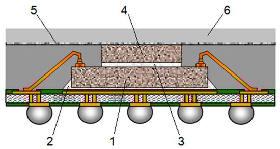
Figure 1.
Extra performance ball grid array (XP-BGA) package. 1, active die; 2, die attach 1; 3, die attach 2; 4 dummy spacer die, stacked gap; 5, heat spreader attach; and 6, heat spreader.
Various types of BGA-like packages have been proposed as follows: high performance (HP), extra performance (XP), plastic (P), multi-chip (MC), and others. These BGA’s were often soldered to moderately complex flexible printed circuit boards (FPCBs) using surface mount technology (SMT) assembly [1,6]. However, around 2005, the thick film ceramic technology based on the BGA format was no longer capable of supporting the rapidly increasing part count and required vertical interconnects.
Three-dimensional (3D) packages have been implemented to meet this need. Internal stacking modules (ISM) are the package stacked and molded within the base package. They often have been used for mobile phone chip sets. For current applications, package-on-package (PoP) are very popular (see Figure 2) [2]. Both ISM and PoP provide adequate connection between dies. However, the number of connections between dies in the 3D stack is limited. In addition, because the connections between different dies go through the substrate, the parasitic load for these connections is high and an appreciable portion of power is consumed by the connection [7].
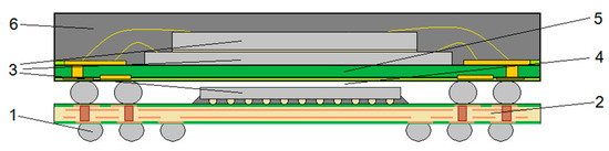
Figure 2.
Package-on-package (PoP) structure. 1, solder balls; 2, laminate; 3, dies; 4, stacked gap; 5, laminate; and 6, mold cap.
In stacked IC-TSV-BGA packages, the through-silicon vias are used for direct vertical connections of the silicon dies. The sizes of the TSVs as compared with the wire bond pads (ISM) or solder bumps (PoP) sizes are significantly smaller, and therefore the parasitic load and input-output (IO) power could be reduced [3].
The comparison between PoP and 3D TSV chip packaging is presented in Figure 3 [4].
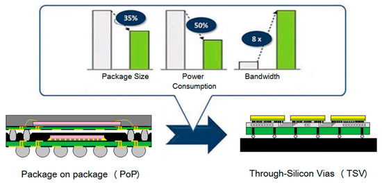
Figure 3.
Three-dimensional integrated circuit (3D IC) vs. PoP.
Embedded die packaging is the next step in further miniaturization and increased functionality of most electronic systems. For the systems with signal frequencies in the order of several GHz and more, much shorter and impedance-matched interconnections are required. This could be achieved using the chip embedding technology based on chip-on-flex organic substrates with high density build-up layers and microvias equipped on both sides with surface mount passive components and active chips in packages (see Figure 4) [5,8].
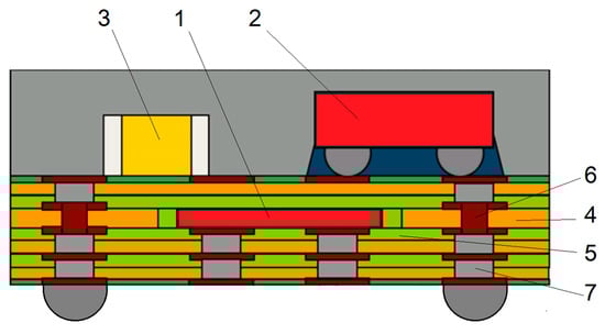
Figure 4.
Embedded die package. 1, Embedded die; 2 BGA die; 3, passive components, 4, polyimide; 5, adhesive; 6, copper; and 7, conductive paste.
On the basis of the presented review, it is seen that the technologies keep the miniaturization trend and advance from a 2D to a 3D system-in-package technology.
The miniaturization of modern LSI circuits leads to an increase in the power dissipation density, which causes their increased heating. The heat drain from electron device active areas is the main factor limiting the device functionality and reliability. The packages are the key elements determining the effectivity of heat dissipation in electronic components and systems. Therefore, the analysis of their thermal modes is of great interest, in particular, the analysis of heat transfer by 3D integrated systems.
2. State of the Art
In this section we analyze the thermal management solutions which have been obtained using computational studies for different types of chip packaging.
2.1. BGA Packages
In [1], the commercial FloTHERM 3.2 version [9] was used to model and simulate the HP- and XP-BGA packages. The sub-modeling technique was used. The global model of the package module was divided into local models. The flip-chip die, heat spreader (metal lid), and solder ball were modeled with 3D elements; the flip-chip bumps and heat source were modeled with 2D elements. Convection-free conditions were taken into consideration. The 2D and 3D temperature maps for the total package and its partial elements were not presented. In [10], thermal modeling of the global 3D constructions of BGA and XP-BGA packages was performed. For comparison, the following two software tools were used: the universal 3D simulator COSMOS and the Overheat BGA program, which are based on the quasi-3D package model. The Pentium 4 CPU time for the XP BGA was 3 h and 15 min, accordingly, it was shown that the quasi-3D models reduced the CPU time by an order of magnitude.
In [11], a simple construction of small outline package (PSOP) combined with a heat spreading mass (copper slag) was simulated using FloTHERM software. The recommendations of package thermal regimes optimization were developed. Unfortunately, the CPU time and the comparison with experimental data were not sited.
2.2. 3D-IC-TSV Packages
In [12], the Cadence general multistep conception of 3D ICs with TSVs design was proposed. Within this conception, thermal analysis is needed to ensure hot spots and thermal leakages are below specified limits.
The following four types of thermal models for 3D-IC-TSV constructions are used: fully numerical FEM [13,14,15], quasi-3D [10,16], analytical [17,18], and based on electro-thermal analogy [19,20].
In [3], the commercial software ABAQUS was used to perform thermo-mechanical simulation and analysis of Xilinx IC-TSV-BGA stack module comprised of FPGA IC, analog IC, and a transceiver. The sub-modeling approach was used to divide the global model into local sub-models. The sub-models effected the convergence of the solution and appropriate accuracy for partial details. The full 3D temperature distribution and 2D temperature cross-sectional views were not presented. The methodology for sewing together the sub-models and forming the global package model was not discussed.
In [21], a numerical 3D model of a two-die 300 mW package with and without TSVs was built using ANSYS. Temperature and heat flux maps were presented. To simplify the solutions, the homogenization and sub-modeling approaches were performed.
The COMSOL software was used for thermal simulation in two- and three-layer stacked middle power [14] and high power [15] ICs.
The special effects for TSVs, i.e., the heat flow detouring around the TSV, Cu pistoning in through-silicon holes, and thermo-mechanical stress caused by thermal heating were investigated in [3,13,21].
Complete thermal modeling of the global IC-TSV-BGA multilayers construction without dividing into local models was performed in [16] using the quasi-3D approach. The full 3D temperature distribution and 2D temperature maps of all the device structure layers were received and analyzed.
In all the works mentioned above, the 3D-IC-TSV modeling procedure was iterated several times until the module offered satisfied performance. Therefore, different thermal model reduction techniques were used to produce lighter models. In [19], the Green function-based analytical spectral method was used assuming the homogeneous thermal conductance of vias. A significant (3–100 times) speed-up over FDM-based thermal simulator COMSOL was achieved. In several works, a combination of analytical and numerical methods was used for thermal modeling of 3D ICs. In [17], a simple analytical model was proposed to estimate the temperature distribution in active layers of IC chips. ANSYS was used for 2D general construction simulation assuming uniform heat generation in the homogeneous medium with constant properties to avoid a convergence problem. In [20], the analytical model assumed heat flow only in vertical directions, and neglected heat spreading in the device plane. Each active die was associated with two significant thermal resistances, i.e., silicon–SOI substrate and metal–SiO2. A numerical solution for the simplified model was used to analyze the role of TSVs in heat dissipation.
2.3. Embedded Die Packages
The general conception “design to manufacturing” of embedded PCBs was developed in the HERMES project (high density integration in embedding chips for reduced size module and electronic systems) [22]. The multistep workflow with a consistent model library was proposed. One of the steps was thermo-mechanical modeling to identify the high stress areas within components at different PCBs. In [23], in addition to the general design workflow the specific features of the power PCB Embedded Technology were discussed. In both publications [22,23], only the results of stress simulation were presented. The thermal models were not discussed, and the results of temperature and heat flow distributions in the embedded die board structures were not presented.
Unfortunately, we did not find publications in which the thermal modeling problem of multi-chip embedded circuit boards was considered completely.
Summarizing the cited above review, we can conclude that the complex problem of heat transfer in 3D packages was numerically solved using the following universal 3D simulation tools: FloTHERM [1,11], COMSOL [14], ANSYS [24], MSC/PATRAN [25], COSMOS [26], and others. However, the assessment of sensitivity to various geometric and material parameters for large finite-difference or finite-element models requires long processor times and large RAM volume. Correct simplification of a 3D thermal model is an effective means of obtaining an accurate solution with acceptable processor time. In this direction lead two ways: a sub-modeling technique (the global model of the package is divided into local models of its functional blocks) and a quasi-3D approach (the 3D problem is reduced to a system of coupled 2D equations for the set of device structure layers).
In this paper, the quasi-3D approach is introduced as an effective way to solve the problem of thermal simulation of the modern 3D-IC-TSV and multi-chip embedded circuit board packages.
3. Quasi-3D Numerical Model of IC Packages
The temperature distribution in the global construction of a 3D IC module is described by the Joule heat transfer 3D partial differential equation:
where λ is the thermal conductivity and P is the power density.
In the multilayer structure (Figure 5), the temperature distribution along the z-axis in each structural layer can be considered to be linear, since layer thickness is much smaller than its horizontal dimensions, i.e., LX, LY ≫ LZ. Due to this, the 3D problem can be reduced to a system of 2D equations on the horizontal surfaces of the layers [10].
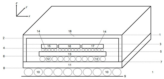
Figure 5.
Geometrical model of the 3D structure of stacked silicon interconnection module. Planes: 1, package top; 2, bottom of package lid; 3, top of dies; 4, bottom of dies; 5, top of passive silicon interposer; 6, bottom of passive silicon interposer; 7, top of substrate; 8, bottom of substrate; 9, surface of PCB; 10, BGA balls; 11, package substrate; 12, C4 bumps; 13, passive silicon interposer; 14, microbumps; 15,16, and 17, active dies; and 18, lid of package.
The system of 2D equations describes the temperature distribution on the top surface of the package T1(x,y), on the surfaces of the package inner layers Tξ(x,y), ξ = 2, …, N, and on the surface of the PCB TN+1(x,y). These equations have the following form:
- convective heat transfer occurs on the top surface of the package
- for inner layerswhere Tξ(x,y) is the layer temperature; TAMB is the ambient temperature; P is the power density on die surface; α is the convective heat transfer coefficient; λξ and zξ are the thermal conductivity coefficient and thickness of the package structural layer ξ = 1,2, …, N; N is the quantity of package layers XS YS package horizontal sizes.
On the PCB surfaces, the temperature is assumed to be constant and equal to the ambient temperature, TN+1(x,y) ≡ TAMB, or other heat exchange conditions are established, for example, a coefficient of convective heat exchange can be set.
Appropriate boundary conditions for Equations (2) and (3) are established on the side surfaces of the package.
The system of partial differential Equations (2) and (3) is solved by the finite difference method. A non-uniform difference grid is generated automatically. The system of linear algebraic equations is solved by the method of successive over relaxation. The software tool guided by 3D IC chip package thermal simulation was developed. The maximum quantity of structural layers is 20 and the difference grid maximum size is 700 × 700 nodes. The software is able to simulate thermal processes in different types of BGA packages, such as 3D integrated IC-TSV-BGA, multi-chip stack embedded PCB, and others.
The input data are the following:
- Package structural parameters, i.e., the number of layers, type of layer, sizes, and physical parameters of the layer;
- The powers or power densities of the active dies;
- Computational parameters, i.e., difference network sizes MX × MY and accuracy of computations.
The output data are the following:
- Temperature arrays in network nodes for each layer Tξ(i,j), ξ = 1,2, …, N;
- The temperature distribution plots Tξ(i,j) in the x,y plane;
- Average TAV and maximal TMAX values of layer temperatures.
The CPU time for a typical BGA package thermal simulation is about 30 min for the IBM PC Intel Core i7. For comparison, the process of simulation using the universal fully-3D simulator ANSYS requires 330 min of CPU time.
4. Simulation Results
The results of using the Q3D package models for thermal simulation of different types of BGA packages have been presented in our previous work [10]. Next, the Q3D modeling results of modern generation chip packages, i.e., stacked IC-TSV-BGAs and multi-chip embedded circuit boards, which are expected to take hold in the industry and become mainstream technologies, are presented [11].
4.1. Stacked IC-TSV-BGA Module
The 3D module under test is shown in Figure 6 and Figure 7. It is similar to the Xilinx module [3] which consists of three active dies (17,18,19 in Figure 6) placed on a passive silicon interposer. The interposer consists of TSVs, metal layers for connecting the die with the die, microbumps for connecting the die with the interposer, and C4 bumps for connecting the interposer with the die. The package sizes are 35 × 35 × 3.25 mm. The total power is 20 W.
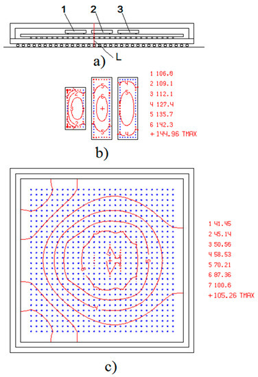
Figure 6.
Distribution of temperature in the structure of stacked IC-TSV-BGA module [16]. (a) Cross-section of the structure. L, the line of the vertical temperature distribution diagram, see Figure 7; (b) Temperature on the active surface of dies, isotherms, °C; (c) Temperature on the top surface of interposer, isotherms, °C. 1, active die with power 4 W; 2, active die with power 8 W; and 3, active die with power 8 W.
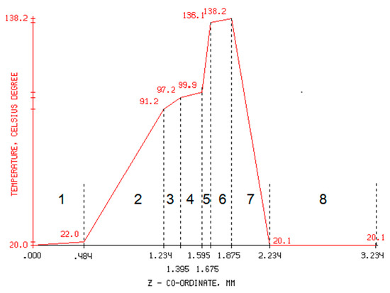
Figure 7.
Vertical temperature distribution along the line L (see Figure 6a) [16]. Package regions: 1, BGA balls; 2, substrate; 3, C4 bumps; 4, interposer; 5, microbumps; 6, active die; 7, air; and 8, package lid.
The thermal conductivities of the package constructive materials are shown in Table 1.

Table 1.
Thermal conductivities of the package constructive materials.
It is interesting to analyze critical temperatures for a multi-chip TSVs stack, i.e., maximal temperatures for the semiconductor dies and the interposer with built-in copper TSVs.
To simplify the thermal analysis of the package structure in Figure 6a, we established at the PCB surface, the condition TPCB = TAMB, neglecting the heat flow caused by a free convection.
In Figure 6b,c, the temperature distributions on the surfaces of active dies with power 8 W (Dies A) and 4 W (Die B) and on the upper surface of a passive silicon interposer are shown. In Figure 7 the temperature distribution along the vertical line L (see Figure 6a) is shown.
The value TMAX = 145 °C observed at the surface of the middle die in Figure 6b is critical because it is very close to that established for the semiconductor ICs’ upper limit of 150 °C. The thermal regime of the middle die must be improved to decrease TMAX.
The copper TSVs integrated into the silicon interposer are sensitive to temperature influence. A primary reliability concern for 3D integration is Cu pistoning as a result of the coefficient of thermal expansion mismatch with Si. Therefore, the temperature of the silicon interposer is the important factor. It is seen in Figure 6c that the TMAX of interposer is about 106 °C, which means that stress and degradation of TSVs cannot appear.
It is necessary to note that the complete thermal solution for the global IC-TSV-BGA construction was obtained [12].
4.2. Multi-Chip Stack Embedding Package
Embedded die modules have enabled continued electronic packaging size reduction while at the same time improved performance. The wafer and board level device embedded (WABE) technology is used to embed die in multi-layer flexible PCB [27]. Three structures of embedded modules were examined.
In Figure 8, the temperature distribution in the structure of a single-layer package with 38 × 38 mm2 total area is shown. The analogous pictures are shown in Figure 9 for the two-layer package with 38 × 20 mm2 area, and in Figure 10 for the three-layer package with 20 × 20 mm2 area. The power of each die is 10 W.
Figure 8.
Thermal mode of chips located in a single-layer package. (a) Cross-section of the structure; (b) Vertical temperature distribution along the line L; (c) Temperature distribution on the active surface of the dies. 1, dies flip-chip; 2, solder balls; 3, substrate-polyimide; 4, vias; and 5, PCB.
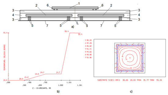
Figure 9.
Thermal mode of chips located in a two-layer package. (a) Cross-section of the structure; (b) Vertical temperature distribution along the line L; (c) Temperature distribution on the active surface of the die lying on the package. 1, upper die flip-chip; 2, lower dies flip-ship; 3, polyimide; 4, adhesive; 5, vias; 6, balls; and 7, PCB.
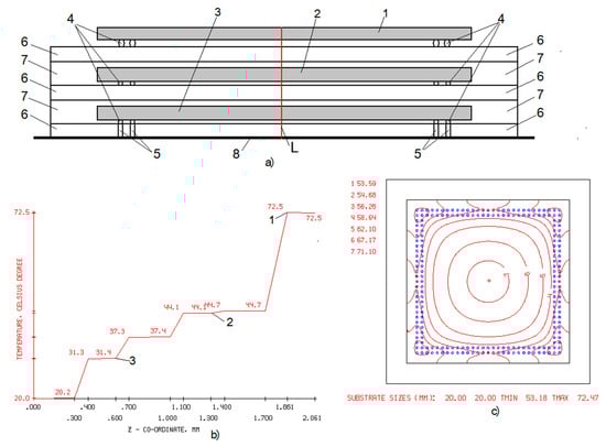
Figure 10.
Thermal mode of chips located in a three-layer package. (a) Cross-section of the structure; (b) Vertical temperature distribution along the line L; (c) Temperature distribution on the active surface of the die lying on the package. 1, upper die flip-chip; 2, middle die flip-chip; 3, lower die flip-chip; 4, solder balls; 5, vias; 6, polyimide; 7, adhesive; and 8, PCB.
The series of Figure 8, Figure 9 and Figure 10 illustrates two facts. Firstly, the stacking technique reduces the total device area in the horizontal plane, twice for the stacked module in Figure 9 and thrice in Figure 10. Secondly, the price of the area reduction is the rapid TMAX increase of the active dies, i.e., 44, 55, and 72 °C for the constructions, presented in Figure 8, Figure 9 and Figure 10 accordingly. The largest value of 72 °C for the structure, shown in Figure 10, correlates well with the experimental value of 85 °C taken for the embedded die module reliability testing in [11,27].
The complete solution of 3D thermal performance in modern multi-chip embedded module fabricated by WABE technology was developed for the first time.
5. Validation of the Q3D Model
The validation of the Q3D model was carried out by the following two ways: (1) comparison with simulated results obtained using standard fully-3D FEM simulators and (2) comparison with measured characteristic temperatures or thermal resistances, i.e., junction to case (ΘJC) and junction to board (ΘJB), for different types of packages.
5.1. Comparison with Results Obtained Using Standard Fully-3D FEM Simulators
For thermal characterization, the TSV-based 3D stacked ICs module, presented in Figure 11a, was selected [14]. The complete model consists of three silicon layers each with the size 1 × 1 × 0.1 mm, 16 TSVs in the form of a 4 × 4 matrix placed on each of the silicon layers, and 64 copper bumps divided into four groups, 4 × 16. The bottom layer of bumps is in contact with the FR4 circuit board and the top layer of bumps is in contact with the heat sink. The silicon die in the model is partitioned into four 2 × 2 matrices of power grids, as shown in Figure 11b. Each grid represents a different function block.
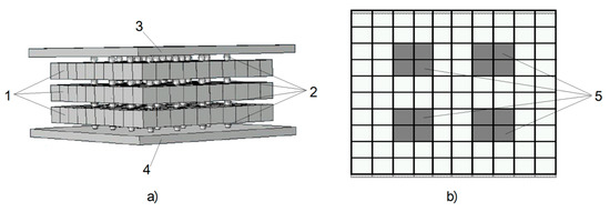
Figure 11.
(a) Three-layer TSV stack model built using COMSOL 4.1 software; 1, TSVs; 2, solder balls; 3, heat sink; and 4, substrate. (b) Die surface; 5, 2 × 2 matrices of power grids.
The 3D view of temperature distribution for three-layer chip in the package obtained using the COMSOL 4.1 software [28] is shown in Figure 12 [14].
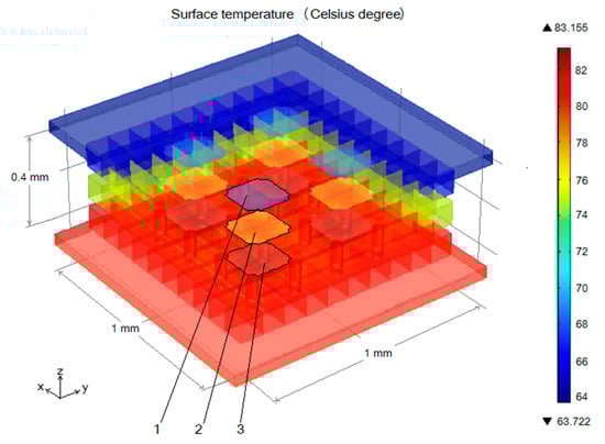
Figure 12.
The 3D view of steady-state temperature distribution for three-layer chip with TSVs; 1, upper silicon layer; 2, central silicon layer; 3, bottom silicon layer.
This module was simulated using the Overheat-3D-IC software tool with a developed quasi-3D model. The temperature distributions on the surfaces of the upper and the bottom silicon layers with TSVs are presented in Figure 13. They are in good agreement with the temperature distribution presented in Figure 12. The comparison with the simulated results obtained using COMSOL software is presented in Table 2.
Figure 13.
The temperature distributions simulated using Overheat-3D-IC. (a) On the upper silicon layer; (b) On the bottom silicon layer.
Table 2.
Comparison of results obtained using COMSOL and Overheat-3D-IC software tools.
It is seen that the Q3D thermal model is valid and gives a solution very close to the complete numerical solution obtained using a standard fully-3D FEM simulator.
In an analogous way, the simulation results were duplicated obtained using FloTHERM for the Analog Devices Power Small Outline Package (PSOP) with sizes 15.9 × 11 × 3.15 mm and total power 2 W working at ambient temperature TAMB = 85 °C [11]. The maximal difference in internal module temperature distributions obtained by two different tools in the range + 85–130 °C was not more than 5–6 °C.
These examples confirm the fact that the developed Q3D thermal model is valid and describes the temperature distribution in different types of 3D IC packages adequately to the fully-3D model.
5.2. Comparison with Measured Thermal Resistances for Different Types of Packages
5.2.1. The Standard BGA Package
The standard 17 × 17 mm2 BGA package was used with 8.2 × 8.2 mm2 die, three-row peripheral ball array, 156 perimeter balls, 16 central thermal balls; the chip power dissipation was 1 W [26]. The comparison of the measured and simulated results for thermal resistance junction to ambient ΘJA is shown in Table 3, showing that good agreement was achieved.
Table 3.
Simulated and measured thermal resistances of 17 × 17 mm2 BGA package.
5.2.2. UltraScale FPBGA Package
Because the Xilinx FSGD2104 package was used as an element of global TSV-IC-BGA module it was selected as the device under test. Simulated and measured thermal resistances ΘJB and ΘJC of the package FSGD2104, which is used for field-programmable gate arrays (FPGA) [26] are presented in Table 4.
Table 4.
Simulated and measured thermal resistances of the package FSGD2104.
It is seen that the proposed quasi-3D thermal model of the package provides the results with reasonable accuracy.
5.3. High-Performance Flip-Chip BGA (HP-fcBGA)
High-performance flip-chip BGA (HP-fcBGA) is a popular package solution for higher pin count and superior heat dissipation. In [1], the measurement results of these packages thermal mode, as well as the results of their simulation using the FloTHERM soft tool were presented. We have compared the measured and simulated by FloTHERM thermal resistance junction to ambient ΘJA with this resistance simulated using our software Overheat-3D-IC. It is seen in Figure 14 that our simulation results are in good agreement with this experiment.
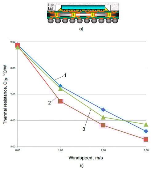
Figure 14.
(a) High-performance flip-chip BGA (HP-fcBGA) structure; (b) Thermal resistance junction to ambient ΘJA. 1, measured; 2, simulated by FloTHERM; and 3, simulated by Overheat-3D-IC.
6. Conclusions
The quasi-3D approach for thermal modeling of 3D integrated circuits systems in package (SiPs) was developed. It takes into account the following specific attributes of modern SiP constructions:
- (a)
- 3D integration of ICs and board;
- (b)
- Large number of thinned layers of different materials;
- (c)
- Vertical z-axes interconnections.
The classic heat-transfer equation for a 3D multilayer structure is reduced to the set of coupled 2D equations for separate construction layers. As a result, the computational difficulties, processor time, and RAM volume are greatly reduced, while saving the accuracy. The software tool Overheat-3D-IC was developed on the base of the generalized Q3D package numerical model.
Two modern types of 3D SiPs, i.e., IC-TSV-BGA and MC-embedded PCB, were analyzed using Overheat-3D-IC and universal 3D simulator COMSOL. For the IC-TSV-BGA, the CPU time was 30 min and 330 min, accordingly. The difference in the TMAX determination was not more than 10%.
The complete 3D thermal solution for the global IC-TSV-BGA construction was obtained. The heating problems for temperature sensitive IC chips and TSVs were discussed using the set of 2D temperature maps. We can confirm that the Q3D analysis is more effective than the sub-modeling analysis used in [3].
The complete 3D thermal simulation of the MC-embedded PCB module fabricated by the novel WABE technology was carried out for the first time. It was shown that multi-chip stack embedding technology cardinally reduced the horizontal area of module, and at the same time increased, in equivalent proportion, the maximal temperatures of the dies.
Validation of the Q3D model was carried out. The simulated and measured values of thermal resistances ΘJA, ΘJB, ΘJC, and maximal temperature TMAX were compared for different types of packages. The simulation error was 10–20%.
In particular, the quasi-3D model is applicable to modern 3D IC packages and also to widely used packages of flip-chip BGA series.
Author Contributions
Project administration, funding acquisition and mathematical model development K.O.P.; mathematical model, algorithm, software tool development and numerical analysis N.I.R.; writing—original draft preparation and review and editing K.O.P. and N.I.R. All authors have read and agreed to the published version of the manuscript.
Funding
This work was implemented in the framework of the Russian Foundation for Basic Research (grants 18-07-00898 A and 20-57-53004).
Conflicts of Interest
The authors declare no conflict of interest.
References
- Krishnamoorthi, S.; Chong, D.Y.R.; Anthony, Y.S. Thermal Management and Characterization of Flip Chip BGA Packages. In Proceedings of the 6th Electronics Packaging Technology Conference (EPTC 2004), Singapore, 8–10 December 2004; Institute of Electrical and Electronics Engineers (IEEE): Piscataway, NJ, USA, 2005; pp. 53–59. [Google Scholar]
- Smith, L. Package on Package (PoP). Applications, Requirements, Infrastructure and Technologies. SMTA OR Charter. March 2011. Available online: https://www.smta.org/chapters/files/Oregon_SMTA_OR_March_16_LSMIT.pdf (accessed on 30 March 2020).
- Madden, L.; Ramalingam, S.; Wu, X.; Wu, E.; Banijamanali, B.; Kim, N.; Abugharbieh, K. Xilinx Stacked Silicon Interconnect Technology Delivers Breakthrough FPGA Performance. Adv. Microelectron. 2013, 40, 6–11. [Google Scholar]
- Garrou, P. 2.5 and 3D IC–The Ultimate Evolution of Chip Packaging. Adv. Microelectron. 2013, 40, 5. [Google Scholar]
- Ostmann, A.; Manessis, D.; Stahr, J.; Beesley, M.; Cauwe, M.; De Baets, J. Industrial and technical aspects of chip embedding technology. In Proceedings of the 2008 2nd Electronics System-Integration Technology Conference, London, UK, 1–4 September 2008; Institute of Electrical and Electronics Engineers (IEEE): Piscataway, NJ, USA, 2008; pp. 315–320. [Google Scholar]
- Ma, Y.Y.; Chong, D.Y.R.; Wang, C.K.; Anthony, Y.S. Development of Ball Grid Array Packages with Improved Thermal Performance Sun. Available online: http://www.utacgroup.com/library/EPTC2005_F2.5_P0149_Thermal_XP-BGA.pdf (accessed on 26 April 2020).
- Amkor Technology. Technology Solutions Package-on-Package (PoP). 2019. Available online: https://c44f5d406df450f4a66b-1b94a87d576253d9446df0a9ca62e142.ssl.cf2.rackcdn.com/2018/02/PoP_DS586.pdf (accessed on 26 April 2020).
- Johansson, S.; Dzarnosski, J.; Itoi, K. Miniaturization of heating aid electronics using embedded die pack-aging. In Proceedings of the SMTA Intern, Rosemont, IL, USA, 25 September 2016; pp. 9–15. [Google Scholar]
- FloTHERM. Mentor Graphics (Deutschland) GmbH. Arnulfstr. 201 80634 München Germany. Available online: https://www.mentor.com/products/mechanical/flotherm/flotherm/ (accessed on 17 May 2020).
- Petrosyants, K.; Rjabov, N. Quasi–3D Approach for BGA Package Thermal Modeling. In Proceedings of the 18th International Workshop on Thermal Investigations of ICs and Systems (THERMINIC 2012), Budapest, Hungary, 25–27 September 2012; pp. 158–161. [Google Scholar]
- Day, R.; Tota, P. Thermal Analysis of a Small Outline Package Mounted on a PCB Using Computational Fluid Dynamics. Eng. Edge 2016, 5, 27–31. [Google Scholar]
- 3D ICs with TSVs–Design Challenges and Requirements. 2011 Cadence Design Systems, Inc. Available online: https://resources.pcb.cadence.com/sigrity-whitepapers/3d-ics-with-tsvs-design-challenges-and-requirements (accessed on 4 May 2020).
- Chien, H.-C.; Lau, J.H.; Chao, Y.-L.; Tain, R.-M.; Dai, M.-J.; Wu, S.-T.; Lo, W.-C.; Kao, M.-J. Thermal Performance of 3D IC Integration with Through-Silicon Via (TSV). J. Microelectron. Electron. Packag. 2012, 9, 97–103. [Google Scholar] [CrossRef]
- Swarup, S.; Tan, S.X.-D.; Liu, Z.; Swarup, S. Thermal characterization of TSV based 3D stacked ICs. In Proceedings of the 2012 IEEE 21st Conference on Electrical Performance of Electronic Packaging and Systems, Tempe, Arizona, USA, 21–24 October 2012; Institute of Electrical and Electronics Engineers (IEEE): Piscataway, NJ, USA, 2012; pp. 335–338. [Google Scholar]
- Vaddina, K.R.; Rahmani, A.-M.; Latif, K.; Liljeberg, P.; Plosila, J. Thermal modeling and analysis of advanced 3D stacked structures. Procedia Eng. 2012, 30, 248–257. [Google Scholar] [CrossRef]
- Petrosyants, K.O.; Ryabov, N.I. Quasi-3D Thermal Model of Stacked IC-TSV-BGA Package. In Proceedings of the 2019 25th International Workshop on Thermal Investigations of ICs and Systems (THERMINIC), Lecco, Italy, 25–27 September 2019; Institute of Electrical and Electronics Engineers (IEEE): Piscataway, NJ, USA, 2019; pp. 1–4. [Google Scholar]
- Im, S.; Banerjee, K. Full chip thermal analysis of planar (2-D) and vertically integrated (3-D) high performance ICs. In Proceedings of the International Electron Devices Meeting 2000. Technical Digest. IEDM (Cat. No.00CH37138), San Francisco, CA, USA, 10–13 December 2000; pp. 727–730. [Google Scholar] [CrossRef]
- Savidis, I. Characterization and Modeling of TSV Based 3-D Integrated Circuits. Ph.D. Thesis, University of Rochester, New York, NY, USA, 2013; p. 443. [Google Scholar]
- Oh, D.; Chen, C.C.P.; Hu, Y.H. Efficient Thermal Simulation for 3-D IC with Thermal through-Silicon Vias. IEEE Trans. Comput. Aided Des. Integr. Circuits Syst. 2012, 31, 1767–1771. [Google Scholar]
- Jain, A.; Jones, R.; Chatterjee, R.; Pozder, S. Analytical and Numerical Modeling of the Thermal Performance of Three-Dimensional Integrated Circuits. IEEE Trans. Compon. Packag. Technol. 2009, 33, 56–63. [Google Scholar] [CrossRef]
- Souare, P.M.; Coudrain, P.; Colonna, J.; Fiori, V.; Farcy, A.; De Crécy, F.; Borbély, A.; Ben-Jamaa, H.; Laviron, C.; Gallois-Garreignot, S.; et al. A comprehensive platform for thermal studies in TSV-based 3D integrated circuits. In Proceedings of the 2014 IEEE International Electron Devices Meeting (IEDM), San Francisco, CA, USA, 15–17 December 2014; pp. 35.4.1–35.4.4. [Google Scholar] [CrossRef]
- Stahr, J.; Morianz, M.; Brizoux, M.; Grivon, A.; Maia, W. Simulation of Embedded Components in PCB Environment and Verification of Board Reliability. Available online: https://silo.tips/download/simulation-of-embedded-components-in-pcb-environment-and-verification-of-board-r (accessed on 26 April 2020).
- Battoy, C.; Martin, C.; Morel, F.; Caillaud, R.; Leslé, J.L.; Mrad, R.; Degrenne, N.; Mollov, S. Application of the PCB Embedding Technology in Power Electronics–State of the Art and Proposed Development. In Proceedings of the Second International Symposium on 3D Power Electronics Integration and Manufacturing (3D PIEM), College Park, MD, USA, 25–27 June 2018; pp. 1–12. [Google Scholar]
- ANSYS Chip-Package-System (CPS) Co-Design and Thermal Management of Electronics 2012. Available online: https://www.ansyscom/Ansys/corporate/resourcelibrary/precentation/chip-package-system-design1012-pres.pdf. (accessed on 10 March 2020).
- Patran Complete FEA Modeling Solution. Available online: https://www.mscsoftware.com/product/patran (accessed on 26 March 2020).
- Elkady, Y.A. Thermal Performance of Ball Grid Arrays and Thin Interface Materials. Ph.D. Thesis, Auburn University, Auburn, AL, USA, 8 August 2005; p. 176. [Google Scholar]
- Tatsuya Ito. Multi-Chip Embedded Circuit Board, “WABE”. SemiCon Taiwan 2016 07.09.2016–09.09.2016. Taipei Nangang Exhibition Center: Taipei, Taiwan. Available online: http://www.semicontaiwan.org/en/ (accessed on 20 March 2020).
- COMSOL. COMSOL, Inc. 100 District Avenue Burlington, MA 01803 USA. Available online: https://www.comsol.com (accessed on 17 May 2020).
- Mechanical and Thermal Design. Guidelines for Lidless Flip-Chip Packages. Application Note. XAPP1301 (v.1.4). 29 April 2019. Available online: https://www.xilinx.com/support/documentation/application_notes/xapp1301-mechanical-thermal-design-guidelines.pdf (accessed on 26 March 2020).


© 2020 by the authors. Licensee MDPI, Basel, Switzerland. This article is an open access article distributed under the terms and conditions of the Creative Commons Attribution (CC BY) license (http://creativecommons.org/licenses/by/4.0/).