Article

Magnetron Sputtered Electron Blocking Layer as an Efficient Method to Improve Dye-Sensitized Solar Cell Performance

1
Research & Development Centre for Photovoltaics, ML System S.A. Zaczernie 190G, 36-062 Zaczernie, Poland
2
Department of Advanced Materials Engineering, Faculty of Physics, Astronomy and Applied Computer Science, Jagiellonian University, Łojasiewicza 11, 30-348 Cracow, Poland
3
Department of Physical Chemistry and Physicochemical Basis of Environmental Engineering, Institute of Environmental Engineering in Stalowa Wola, John Paul II Catholic University of Lublin, Kwiatkowskiego 3A, 37-450 Stalowa Wola, Poland
*
Author to whom correspondence should be addressed.
Energies 2020, 13(11), 2690; https://doi.org/10.3390/en13112690
Submission received: 22 April 2020 / Revised: 24 May 2020 / Accepted: 25 May 2020 / Published: 27 May 2020
(This article belongs to the Special Issue Advanced Dye-Sensitized Solar Cells)

Abstract

:
The main efficiency loss is caused by an intensive recombination process at the interface of fluorine-doped tin oxide (FTO) and electrolyte in dye-sensitized solar cells. Electrons from the photoanode can be injected back to the redox electrolyte and, thus, can reduce the short circuit current. To avoid this, the effect of the electron blocking layer (EBL) was studied. An additional thin film of magnetron sputtered TiO2 was deposited directly onto the FTO glass. The obtained EBL was characterized by atomic force microscopy, scanning electron microscopy, optical profilometry, energy dispersive spectroscopy, Raman spectroscopy and UV-VIS-NIR spectrophotometry. The results of the current–voltage characteristics showed that both the short circuit current (Isc) and fill factor (FF) increased. Compared to traditional dye-sensitized solar cell (DSSC) architecture, the power conversion efficiency (η) increased from 4.67% to 6.07% for samples with a 7 × 7 mm2 active area and from 2.62% to 3.06% for those with an area of 7 × 80 mm2.

1. Introduction

After approximately 30 years of research, dye-sensitized solar cells (DSSCs) have maintained their strong importance among scientific and engineering groups across the world. Many approaches have tried to refine the Grätzel [1] architecture of a dye-sensitized mesoporous titanium oxide layer with an iodine-based electrolyte and platinum counter electrode. A significant increase in efficiency would not have been possible without new dyes, whose absorption spectra better match the spectral distribution of both synthetic [2,3] and natural [4] sunlight. Much work has been devoted to improving electrode performance. New wide bandgap semiconductors with different morphologies (e.g., in nanowires, nanotubes, and nanospheres) have been tested [5]. Various electrolyte formulations have been developed and tested in order to improve DSSC performance, increase their lifetime, and reduce their toxicity [6,7].
Besides chemical stability and technical durability (e.g., a time-dependent decrease in power conversion efficiency (PCE) [8,9] or the leakage of liquid electrolytes due to the unsealing of the cells [10]), some typical physical challenges [11,12] are yet to be solved. A frequently reported mechanism that leads to a decrease in DSSC efficiency is the electron–electrolyte recombination process.
In an ideal model, the photoexcited electrons in dyes are injected into a wide bandgap n-type semiconductor layer, typically TiO2, ZnO or SnO2, and are then transferred to a fluorine-doped tin oxide (SnO2:F, FTO) working electrode, while the holes created in the dye are filled by electrons from the triiodide present in the redox electrolyte ( 2 e + I 3 3 I ). Unfortunately, there are several possible paths through which electrons recombine. The most significant of these are recombinations at the TiO2/electrolyte and FTO/electrolyte interfaces. To challenge these pathways, the concept of the electron blocking layer (EBL) was developed. The role of this layer is to block electrons from being injected back into the electrolyte by providing more preferable transport to the FTO via an appropriate band structure.
The EBL can be set directly on a mesoporous n-type semiconductor [13] or on the FTO surface [14]. There are two main conditions that need to be fulfilled. Firstly, the layer must be continuous to prevent FTO contact with the electrolyte, and secondly, the layer has to be thin enough to avoid high ohmic resistance. The latter factor could lower the open circuit voltage (Uoc) and short circuit current (Isc) due to a greater probability of recombination from structural defects. The blocking layers deposited on mesoporous TiO2 are generally represented by wide bandgap isolators, such as Al2O3 or HfO2 [15], Zn2SnO4 [16], MgO [17] or doped ZnO [18]. Indeed, it is difficult to produce a continuous layer on a mesoporous structure. CVD methods are the most promising because the reaction gas is able to overlay the whole surface exposed to the gas. However, toxic or hazardous precursors and by-products are often a great complication of this technique. Additionally, the required high temperature (in the range of several hundred degrees Celsius) for the CVD growth process could significantly influence the other layers. Thus, it is much simpler to prepare an electron blocking layer directly onto the planar FTO glass, as shown in Figure 1. As reported by Zhu [19], the dominant recombination process occurs at the substrate/electrolyte interface rather than across the TiO2 matrix. Numerous methods have been commonly used for EBL compact layer preparation, such as sol-gel [20], chemical vapor deposition [21], spray-coating [22], and electrodeposition [23]. Low-cost depositions are typically considered to be the most promising, but they do not provide a process that is highly repeatable, while the parameters, such as thickness, stoichiometry and purity of the layer, are crucial. Among the many potential techniques, the magnetron sputtering method [24,25] seems to be the best choice because of its simplicity of use and repeatability. It is necessary to choose an appropriate material as an EBL. For instance, SnO2 [26], ZnO [27] or Nb2O5 [28] were recently reported. However, TiO2 is suggested to be the best EBL due to its low cost, chemical inertness to electrolytes, easy availability, good n-type conductivity and matching electronic band structure to the photoanode.
Herein, a TiO2 RF magnetron sputtered layer was investigated as an electron blocking layer in screen-printed dye-sensitized solar cells. The results, presented in the following sections, were obtained by the current–voltage characteristics (U–I), scanning electron microscopy (SEM), atomic force microscopy (AFM), optical profilometry (OP), energy dispersion spectroscopy (EDS), Raman spectroscopy (RS) and UV-VIS-NIR spectrophotometry. In this paper, two sizes of the active layer were studied—small- and large-scale solar cells with dimensions 7 × 7 mm2 and 7 × 80 mm2. The power conversion efficiency, as a result of the additional electron blocking layer, was increased by 30% and 17%, respectively.

2. Materials and Methods

2.1. RF Magnetron Sputtered Electron Blocking Layer Preparation

The TiO2 compact layer was prepared on the FTO glass (TEC A7, 6–8 Ω/□). The substrates were ultrasonicated in acetone and isopropanol for 5 min and 15 min, respectively. Then, they were transferred to a glove box immediately. The electron blocking layer was sputtered by a Mini SPECTROS™ magnetron system from the TiO2 target (99.99% pure, Kurt J. Lesker Company®, Jefferson Hills, USA). The chamber was pumped down to about 10−5 Torr. A time of 5 min of pre-sputtering was applied to remove any possible contaminants from the target surface. The RF sputtering was carried out at 300 °C to enhance adhesion and, thus, electric contact between the two layers. The parameters of the process were set as a 3 m Torr argon working gas pressure under a power of 100 W. The deposition time was tuned to receive a layer of approximately 30 nm, which was reported as the most efficient thickness for the EBL [29].

2.2. Dye-Sensitized Solar Cell Fabrication

The FTO glass (cleaned as described above) was used to fabricate the working and counter electrodes. Mesoporous TiO2 film was deposited using the screen printing method [30] from titania paste (18NR-T, Greatcell Solar, Elanora, Australia) and sintered up to 565 °C. The obtained thickness of 11 µm was determined by a stylus profilometer (Bruker DektakXT, Billerica, USA). According to the manufacturer’s datasheet, anatase nanoparticles dispersed in the paste have an average size of 20 nm. Samples were immersed for 24 h in a 10−4 M ethanolic solution of ruthenium dye (N719, Greatcell Solar, Elanora, Australia) at room temperature. The layers were then rinsed with ethanol to remove the un-adhered molecules. A counter electrode was prepared by the same printing method using a platinum paste (PT1, Greatcell Solar, Elanora, Australia). A 60 µm lamination foil (DuPont Surlyn®, Wilmington, USA) was used to seal both electrodes. The DSSCs were filled with a commercially available iodine-based redox electrolyte (EL-HPE, DyeSol, Elanora, Australia).

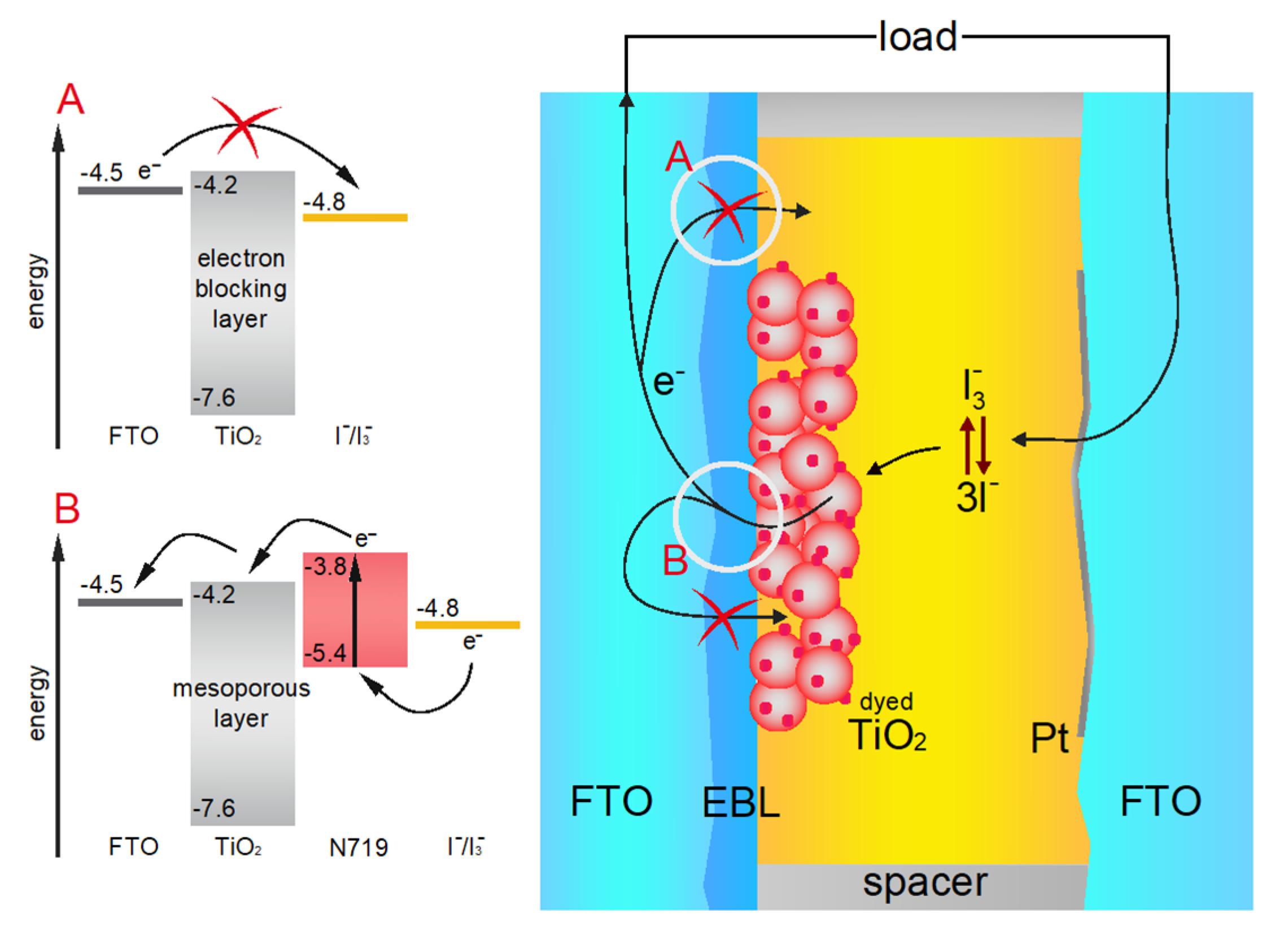
3. Results and Discussion

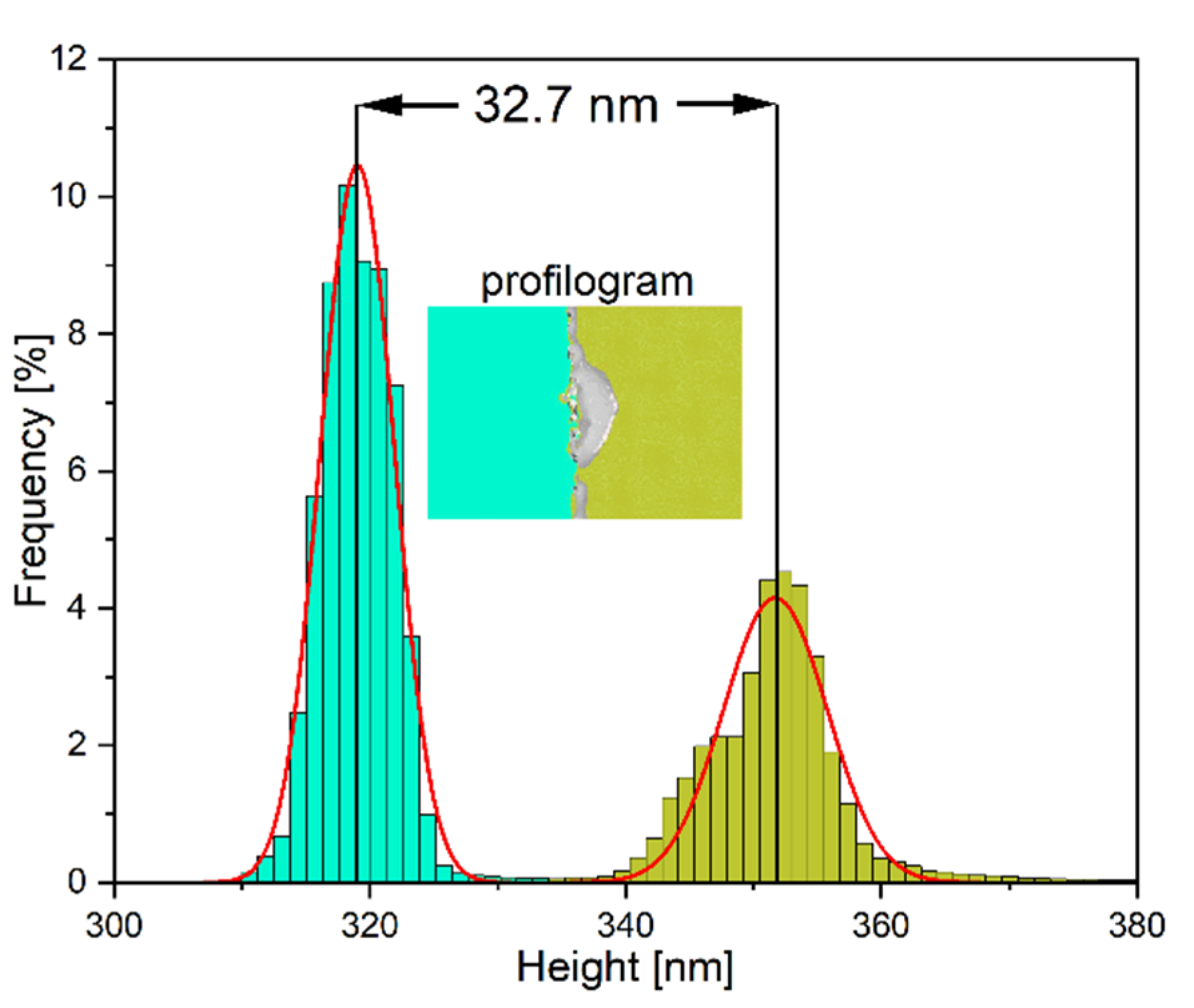
3.1. Measurement of TiO2 Electron Blocking Layer Thickness

The thickness of the magnetron sputtered nanometric TiO2 thin film was determined by an optical profilometer (Profilm3D, Filmetrics, San Diego, USA) in the white light interferometry (WLI) mode. Before deposition, the edge of the FTO glass was covered by polyimide tape and then removed. Additionally, the taped area was slightly cleaned by isopropyl alcohol to remove any glue residue. Then, the step height was imaged on a profilometer. The received data were used to prepare the height histogram presented in Figure 2. The cyan color represents the bare FTO surface and the olive indicates the FTO covered by TiO2. The grey area was not included in the calculations because of the irregular layer surface corrupted by detaching the tape. Two Gauss functions were fitted to the obtained peaks. The difference between the peak positions, calculated to be 32.7 nm, was considered as the thickness of the TiO2 layer.

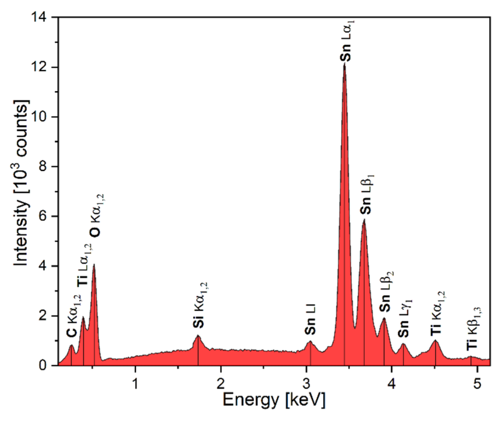
3.2. Energy Dispersive Spectroscopy (EDS) Spectrum

The energy dispersive spectroscopy (SwiftEDS 300, Oxford Instruments, High Wycombe, UK, beam energy 15 kV) outcome, shown in Figure 3, was obtained from a sample with a TiO2/FTO/glass stack. The signal from the carbon (C) element is a result of the atmospheric adsorption of carbon dioxide because the sample was not heated before its transition to the EDS chamber. The small peak from silicon (Si) came from the glass substrate, which, in fact, is a silica. The observed oxygen (O) signal came simultaneously from the CO2 adsorbate and the TiO2, SnO2:F and SiOx layers.
The broad multipeak signal from tin (Sn) was caused by the FTO’s presence in the analyzed sample. The manufacturer’s datasheet suggests that the FTO film is approximately 250 nm. This significant thickness, compared to the electron penetration depth, explains why the Sn signal has the greatest importance in the obtained spectrum. The most important piece of information from the received spectrum is that the TiO2 thin film is present in the sample. This is observable in the three peaks that are tabulated in Table 1. Lines with double numeration are a superposition of two signals with similar energy. For instance, the peaks for O are a superposition of Kα1 and Kα2 transitions.

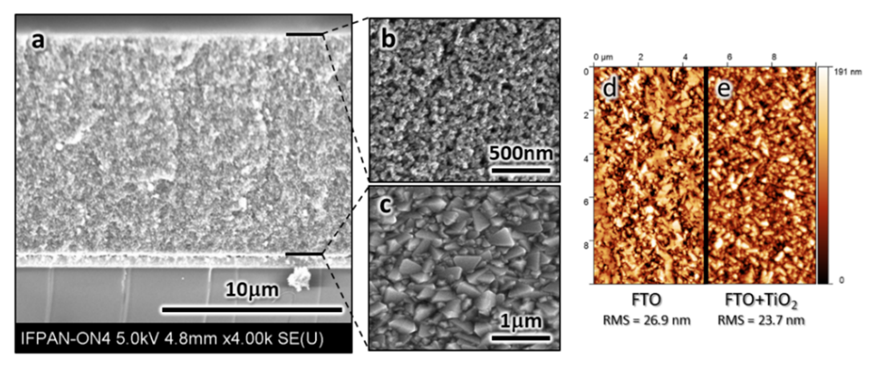
3.3. Scanning Electron Microscopy (SEM) and Atomic Force Microscopy (AFM) Images

The electron blocking layer’s morphology was studied with a scanning electron microscope (Quanta™ 3D FEG, ThermoFisher Scientific, Hillsboro, USA) before the deposition of the mesoporous TiO2. The topography, shown in Figure 4c, is similar to that of the bare FTO, which was also observed by Choi et al. [31]. The reason for this result is the FTO’s high roughness. Because of this roughness, covering the FTO with a thin film of material would not significantly influence the RMS parameter. The roughness of the titanium oxide EBL was measured by an atomic force microscope in tapping mode (Agilent 5500, Agilent Technologies, Santa Clara, USA). The RMS decreased slightly from 26.9 nm for the bare FTO to 23.7 nm for a stack of the 30 nm TiO2 compact layers on the FTO. The intersection, seen in Figure 4a, contains all of the photoanode layers (from the bottom: glass, FTO, TiO2 compact and TiO2 mesoporous layers). In reference to the profilometer measurement, the thickness of the mesoporous film was also confirmed to be approximately 11 µm. The morphology of the sintered TiO2 nanoparticles with an average diameter of 20 nm can be observed in Figure 4b.

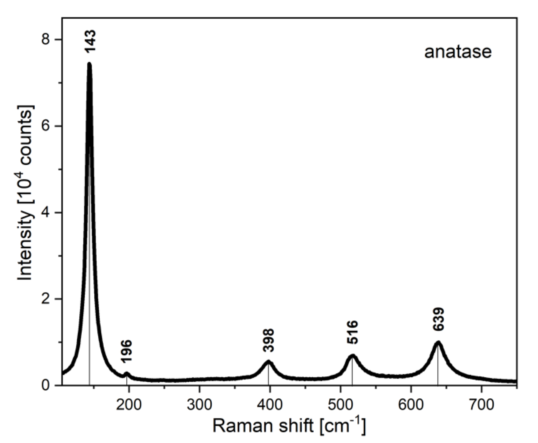
3.4. Raman Spectrum of Electron Blocking Layer

The polymorphism of the titanium oxide electron blocking layer was investigated by Raman spectroscopy. The measurements were made using an integrated Raman spectroscope (LabRAM, HORIBA, Kyoto, Japan). The source used for the measurements was a He–Ne laser with a wavelength of 632.8 nm at 17 mW power. The whole system was complemented by a confocal microscope coupled with an 800 nm focused lens and a two-dimensional multichannel CCD detector. Additionally, the system was equipped with an automatic Czerny–Turner spectrograph with a slot width of 30 mm for a wide–flat field of view. The measurements were taken at room temperature.
According to other studies [32], the obtained spectrum of TiO2, shown in Figure 5, was characteristic for anatase. The active vibrations were located at 143 cm−1 (Eg), 196 cm−1 (Eg), 398 cm−1 (B1g), 516 cm−1 (A1g) and 639 cm−1 (Eg). The provided measurements allowed us to confirm that the TiO2 mesoporous and TiO2 electron blocking layer had the same polymorph. The selfsame polymorph should lead to good electric contact after the sintering process under a high temperature because of matching in the conduction bands’ levels and the crystal structures of both materials.

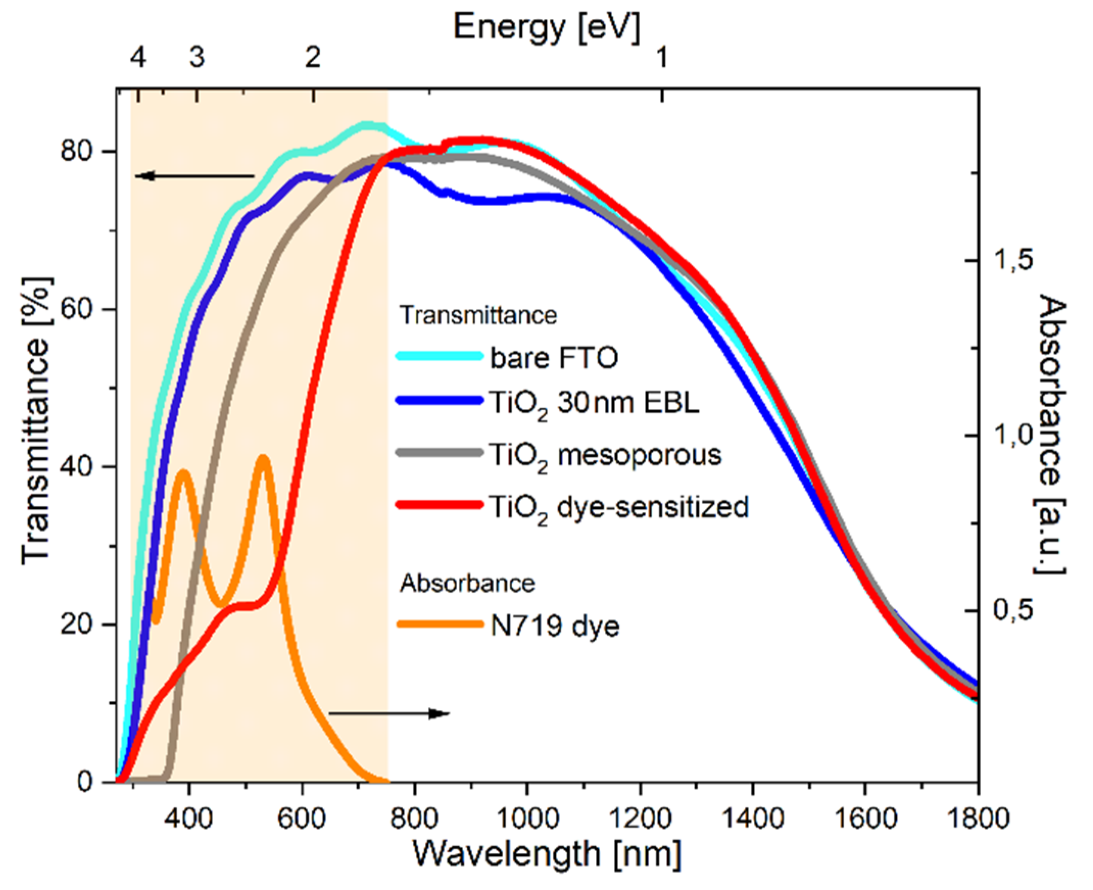
3.5. Transmittance and Absorbance Spectra of the Photoanode

Because the light pathway to the dye leads through the whole photoanode, UV-VIS-NIR spectrophotometry (Jasco V-670 with deuterium and halogen lamps) was used to measure the transmittance for each layer. The signal was averaged from a spot size of a 3 × 3 mm2 area. Figure 6 presents the transmittance versus the wavelength spectrum of compositions from bare FTO up to FTO covered by a dye-sensitized TiO2 layer. Just a slight decrease in transmitted light was observed for the additional 30 nm TiO2 film in the dye absorption wavelength range, which indicates that the EBL layer has no significant influence on the amount of light transmitted to the N719 molecules. Measured absorption peaks near the 390 nm and 530 nm are consistent with those reported by other studies [33,34]. The dye absorbance was measured for a 10−4 M ethanolic solution (99.8% ethanol, Honeywell, Charlotte, USA) in a quartz cuvette with 1 cm of optical thickness.

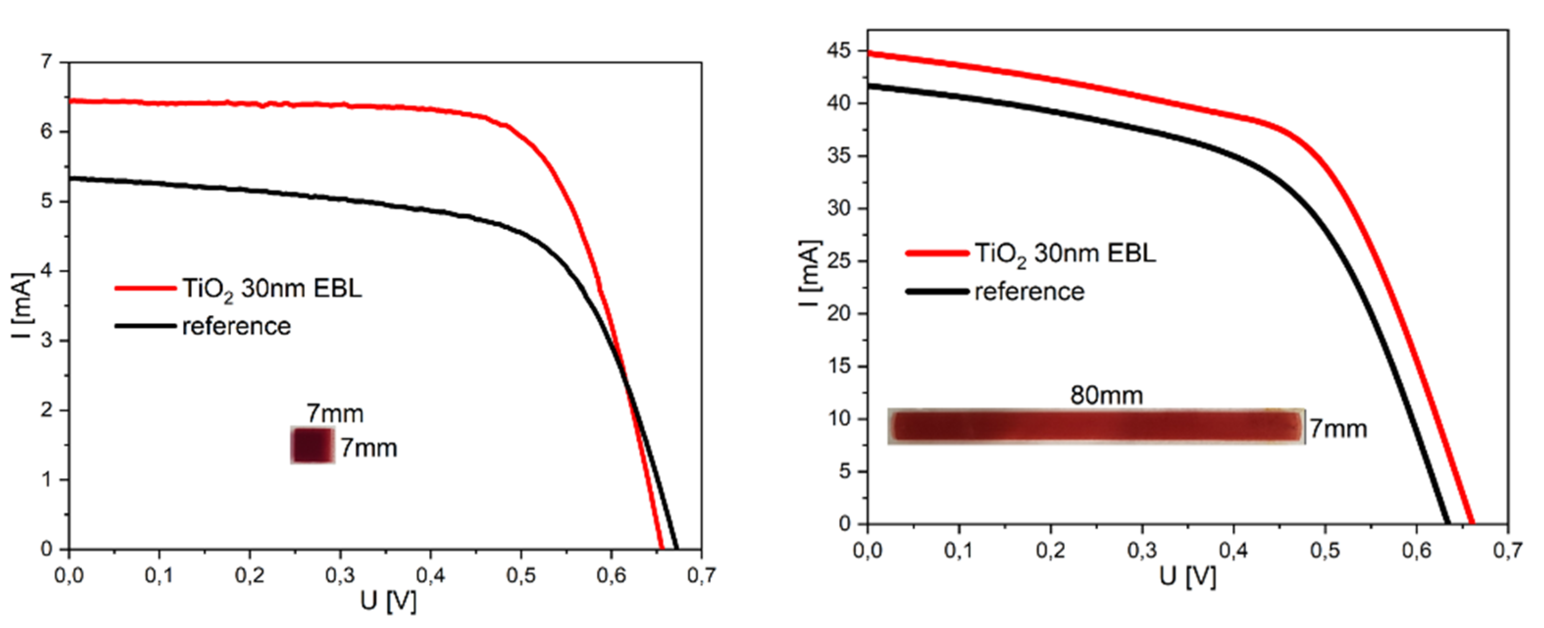
3.6. Performance of the DSSC Devices

The performance of the DSSC devices was investigated by a solar simulator (CLASS-01, PV Test Solutions) under AM1.5 illumination with a light intensity of 100 mW/cm2. The received current–voltage (U–I) characteristics are shown in Figure 7. In both cases, the open circuit voltage did not significantly change because the mesoporous and compact TiO2 layers have similar conduction and valence band levels. Likewise, no difference in Uoc was reported by other groups for ZnO and TiO2 EBLs [35]. Because the main factor for this parameter is the difference between the mesoporous TiO2 and redox electrolyte energy band levels [36], the n-type metal oxide thin film on the FTO should not have a strong effect on the Uoc.
As recently shown, a thin layer of TiO2 on the FTO electrode significantly increases the onset of cathodic dark current, pointing to the increase in a potential barrier to the electron transfer from the FTO to the electrolyte [37]. In our studies the presence of the electron blocking layer significantly increased the short circuit current (Isc) and, as a consequence, also increased the fill factor (FF). For small samples, an increase from 5.33 mA to 6.44 mA and from 0.64 to 0.70 was observed, respectively. For larger samples, the same parameters increased from 41.67 mA to 44.80 mA and from 0.55 to 0.58, respectively. In both cases, the improvement of those parameters indicates that the recombination process was considerably mitigated. As mentioned above, the power conversion efficiency (η) increased by 30% and 17%, depending on the sample size. Because of the larger surface, there is a higher probability of the electrons being scattered or recombined, especially due to the crystal structure’s defects. The longer path to the electrodes may also cause a relaxation, with incidentally met holes in the FTO. We attempted to mitigate this problem via the preparation of a silver electrode along the active area’s edge. The role of this electrode was to collect the photogenerated electrons, possibly close to the place where they were excited. The measurement errors, presented in Table 2, were calculated by standard deviation. The parameters were obtained from eight samples for every type of DSSC device.

4. Conclusions

A thin film of TiO2 was studied as an efficient electron blocking layer. Due to its simplicity of use and high repeatability, RF magnetron sputtering was chosen as the deposition method. A 30 nm thick layer was sputtered on bare FTO and then dye-sensitized solar cells were fabricated by a screen printing technique. The UV-VIS-NIR spectrophotometry transmittance spectra showed no significant influence on the amount of light provided through the photoanode to the dye molecules in its absorbance wavelength range. In both cases of the active area (7 × 7 mm2 and 7 × 80 mm2), an increase in power conversion efficiency due to decreased recombination (and thus an increased short circuit current) was reported. Because of the larger area, the cross section of recombination for mechanisms other than the FTO/electrolyte interface has greater importance. Thus, the percentage growth of efficiency was higher for small samples (30%) than for larger ones (17%).
DSSCs, as third generation solar cells, provide a great opportunity to serve as low-cost and common photovoltaics and could displace silicon-based devices. Present and future works will certainly improve both the efficiency and stability of DSSCs. However, there are still many physical, chemical and technical problems that need to be resolved to deploy these devices into line production and distribute them to private consumers.

Author Contributions

Conceptualization, D.A., J.D. and P.K.; writing—original draft preparation, data curation, formal analysis, investigation, resources—sample preparation and visualization, D.A.; methodology, J.D.; project administration, funding acquisition and validation, P.K. and J.D.; supervision and writing—review and editing, P.K. and J.R. All authors have read and agreed to the published version of this manuscript.

Funding

This work was supported by The National Centre for Research and Development (grant no. TECHMATSTRATEG1/347431/14/NCBR/2018), received as part of the Strategic Research and Development Program “Modern material technologies”—“Efficient and light photo-rechargeable electric energy storage systems based on solar cell-lithium ion battery or solar cell-supercapacitor structures for special applications”. D.A. acknowledges the financial support by The Ministry of Science and Higher Education (grant no. 0046/DW/2018/0).

Conflicts of Interest

The authors declare no conflict of interest. The funders had no role in the design of the study, in the collection, analyses or interpretation of data, in the writing of the manuscript or in the decision to publish the results.

References

  1. O’Regan, B.; Grätzel, M.; Gr, M. A low-cost, high-efficiency solar cell based on dye-sensitized colloidal TiO2 films. Nature 1991, 353, 737–740. [Google Scholar] [CrossRef]
  2. Qina, Y.; Peng, Q. Ruthenium Sensitizers and Their Applications in Dye-Sensitized Solar Cells. Int. J. Photoenergy 2012, 2012, 1–21. [Google Scholar] [CrossRef] [Green Version]
  3. Urbani, M.; Ragoussi, M.-E.; Nazeeruddin, M.K.; Torres, T. Phthalocyanines for dye-sensitized solar cells. Coord. Chem. Rev. 2019, 381, 1–64. [Google Scholar] [CrossRef]
  4. Maddah, H.A.; Berry, V.; Behura, S.K. Biomolecular photosensitizers for dye-sensitized solar cells: Recent developments and critical insights. Renew. Sustain. Energy Rev. 2020, 121, 109678. [Google Scholar] [CrossRef]
  5. Thomas, S.; Kalarikkal, N.; Wu, J.; Sakho, E.H.M.; Oluwafemi, S.O. Nanomaterials for Solar Cell Applications; Elsevier: Amsterdam, The Netherlands, 2019; ISBN 978-012813337-8. [Google Scholar] [CrossRef]
  6. Iftikhar, H.; Sonai, G.G.; Hashmi, S.G.; Nogueira, A.F.; Lund, P. Progress on Electrolytes Development in Dye-Sensitized Solar Cells. Materials 2019, 12, 1998. [Google Scholar] [CrossRef] [Green Version]
  7. Bella, F.; Gerbaldi, C.; Barolo, C.; Grätzel, M. Aqueous dye-sensitized solar cells. Chem. Soc. Rev. 2015, 44, 3431–3473. [Google Scholar] [CrossRef] [Green Version]
  8. Wu, J.H.; Lan, Z.; Lin, J.M.; Huang, M.L.; Hao, S.C.; Sato, T.; Yin, S. A Novel Thermosetting Gel Electrolyte for Stable Quasi-Solid-State Dye-Sensitized Solar Cells. Adv. Mater. 2007, 19, 4006–4011. [Google Scholar] [CrossRef]
  9. Tsai, C.-H.; Lu, C.-Y.; Chen, M.-C.; Huang, T.-W.; Wu, C.-C.; Chung, Y.-W. Efficient gel-state dye-sensitized solar cells adopting polymer gel electrolyte based on poly(methyl methacrylate). Org. Electron. 2013, 14, 3131–3137. [Google Scholar] [CrossRef]
  10. Yang, H.; Huang, M.; Wu, J.-H.; Lan, Z.; Hao, S.; Lin, J. The polymer gel electrolyte based on poly(methyl methacrylate) and its application in quasi-solid-state dye-sensitized solar cells. Mater. Chem. Phys. 2008, 110, 38–42. [Google Scholar] [CrossRef]
  11. Hagfeldt, A.; Boschloo, G.; Sun, L.; Kloo, L.; Pettersson, H. Dye-Sensitized Solar Cells. Chem. Rev. 2010, 110, 6595–6663. [Google Scholar] [CrossRef]
  12. Kavan, L. Electrochemistry and dye-sensitized solar cells. Curr. Opin. Electrochem. 2017, 2, 88–96. [Google Scholar] [CrossRef]
  13. Ramasamy, P.; Kang, M.-S.; Cha, H.-J.; Kim, J. Highly efficient dye-sensitized solar cells based on HfO2 modified TiO2 electrodes. Mater. Res. Bull. 2013, 48, 79–83. [Google Scholar] [CrossRef]
  14. Yang, Y.; Peng, X.; Chen, S.; Lin, L.; Zhang, B.; Feng, Y. Performance improvement of dye-sensitized solar cells by introducing a hierarchical compact layer involving ZnO and TiO2 blocking films. Ceram. Int. 2014, 40, 15199–15206. [Google Scholar] [CrossRef]
  15. Shanmugam, M.; Baroughi, M.F.; Galipeau, D. Effect of atomic layer deposited ultra thin HfO2 and Al2O3 interfacial layers on the performance of dye sensitized solar cells. Thin Solid Films 2010, 518, 2678–2682. [Google Scholar] [CrossRef]
  16. Tan, B.; Toman, E.; Li, Y.; Wu, Y. Zinc Stannate (Zn2SnO4) Dye-Sensitized Solar Cells. J. Am. Chem. Soc. 2007, 129, 4162–4163. [Google Scholar] [CrossRef]
  17. Tennakone, K.; Bandara, J.; Bandaranayake, P.K.M.; Kumara, G.; Konno, A. Enhanced Efficiency of a Dye-Sensitized Solar Cell Made from MgO-Coated Nanocrystalline SnO2. Jpn. J. Appl. Phys. 2001, 40, L732–L734. [Google Scholar] [CrossRef]
  18. Arifin, Z.; Suyitno, S.; Hadi, S.; Sutanto, B. Improved Performance of Dye-Sensitized Solar Cells with TiO2 Nanoparticles/Zn-Doped TiO2 Hollow Fiber Photoanodes. Energies 2018, 11, 2922. [Google Scholar] [CrossRef] [Green Version]
  19. Zhu, K.; Schiff, E.; Park, N.-G.; Van De Lagemaat, J.; Frank, A.J. Determining the locus for photocarrier recombination in dye-sensitized solar cells. Appl. Phys. Lett. 2002, 80, 685–687. [Google Scholar] [CrossRef] [Green Version]
  20. Gu, Z. (Allison); Gao, X.; Li, X.-M.; Jiang, Z.-W.; Huang, Y.-D. Nanoporous TiO2 aerogel blocking layer with enhanced efficiency for dye-sensitized solar cells. J. Alloy. Compd. 2014, 590, 33–40. [Google Scholar] [CrossRef]
  21. Kim, K.E.; Jang, S.-R.; Park, J.; Vittal, R.; Kim, K.-J. Enhancement in the performance of dye-sensitized solar cells containing ZnO-covered TiO2 electrodes prepared by thermal chemical vapor deposition. Sol. Energy Mater. Sol. Cells 2007, 91, 366–370. [Google Scholar] [CrossRef]
  22. Ito, S.; Liska, P.; Comte, P.; Charvet, R.; Pechy, P.; Bach, U.; Schmidt-Mende, L.; Zakeeruddin, S.M.; Kay, A.; Nazeeruddin, M.K.; et al. Control of dark current in photoelectrochemical (TiO2/I--I3-) and dye-sensitized solar cells. Chem. Commun. 2005, 34, 4351–4353. [Google Scholar] [CrossRef] [Green Version]
  23. Jang, K.-I.; Hong, E.; Kim, J.H. Effect of an electrodeposited TiO2 blocking layer on efficiency improvement of dye-sensitized solar cell. Korean J. Chem. Eng. 2012, 29, 356–361. [Google Scholar] [CrossRef]
  24. Meng, L.; Li, C. Blocking Layer Effect on Dye-Sensitized Solar Cells Assembled with TiO2 Nanorods Prepared by dc Reactive Magnetron Sputtering. Nanosci. Nanotechnol. Lett. 2011, 3, 181–185. [Google Scholar] [CrossRef] [Green Version]
  25. Kment, Š.; Krýsová, H.; Hubicka, Z.; Kmentová, H.; Kavan, L.; Zbořil, R. Very thin thermally stable TiO 2 blocking layers with enhanced electron transfer for solar cells. Appl. Mater. Today 2017, 9, 122–129. [Google Scholar] [CrossRef]
  26. Duong, T.-T.; Choi, H.-J.; He, Q.-J.; Le, A.-T.; Gil Yoon, S. Enhancing the efficiency of dye sensitized solar cells with an SnO2 blocking layer grown by nanocluster deposition. J. Alloy. Compd. 2013, 561, 206–210. [Google Scholar] [CrossRef]
  27. Yeoh, M.-E.; Chan, K.Y. Efficiency Enhancement in Dye-Sensitized Solar Cells with ZnO and TiO2 Blocking Layers. J. Electron. Mater. 2019, 48, 4342–4350. [Google Scholar] [CrossRef]
  28. Chun, J.H.; Kim, J.S. Comparison of different structures of niobium oxide blocking layer for dye-sensitized solar cells. J. Nanosci. Nanotechnol. 2014, 14, 6226–6230. [Google Scholar] [CrossRef]
  29. Kim, J.; Choi, H.; Nahm, C.; Moon, J.; Kim, C.; Nam, S.; Jung, D.-R.; Park, B. The effect of a blocking layer on the photovoltaic performance in CdS quantum-dot-sensitized solar cells. J. Power Sources 2011, 196, 10526–10531. [Google Scholar] [CrossRef]
  30. Dziedzic, J. Deposition methods of TiO2 on the glass and characterisation of conductive layer in DSSC. Elektronika Konstr. Technol. Zastos. 2018, 1, 8–10. [Google Scholar] [CrossRef]
  31. Choi, H.; Nahm, C.; Kim, J.; Moon, J.; Nam, S.; Jung, D.-R.; Park, B. The effect of TiCl4-treated TiO2 compact layer on the performance of dye-sensitized solar cell. Curr. Appl. Phys. 2012, 12, 737–741. [Google Scholar] [CrossRef]
  32. Tian, F.; Zhang, Y.; Zhang, J.; Pan, C. Raman Spectroscopy: A New Approach to Measure the Percentage of Anatase TiO2 Exposed (001) Facets. J. Phys. Chem. C 2012, 116, 7515–7519. [Google Scholar] [CrossRef]
  33. Katoh, R.; Yaguchi, K.; Furube, A. Effect of dye concentration on electron injection efficiency in nanocrystalline TiO2 films sensitized with N719 dye. Chem. Phys. Lett. 2011, 511, 336–339. [Google Scholar] [CrossRef]
  34. Katoh, R.; Fuke, N.; Furube, A.; Koide, N. Effect of dye coverage on photo-induced electron injection efficiency in N719-sensitized nanocrystalline TiO2 films. Chem. Phys. Lett. 2010, 489, 202–206. [Google Scholar] [CrossRef]
  35. Seo, H.; Son, M.-K.; Park, S.; Chebrolu, V.T.; Shiratani, M. The blocking effect of charge recombination by sputtered and acid-treated ZnO thin film in dye-sensitized solar cells. J. Photochem. Photobiol. A Chem. 2012, 248, 50–54. [Google Scholar] [CrossRef]
  36. Voloshin, M.V.R.R.A. Components of Natural Photosynthetic Apparatus in Solar Cells. Appl. Photosynth. New Prog. 2016, 9, 161–188. [Google Scholar] [CrossRef] [Green Version]
  37. Kavan, L.; Zivcova, Z.V.; Zlamalova, M.; Zakeeruddin, S.M.; Grätzel, M. Electron-Selective Layers for Dye-Sensitized Solar Cells Based on TiO2 and SnO2. J. Phys. Chem. C 2020, 124, 6512–6521. [Google Scholar] [CrossRef]
Figure 1. Schematic representation of the fabricated dye-sensitized solar cell (DSSC) devices with an additional electron blocking layer (EBL). As presented in diagram A, the EBL prevents electrons from being injected back from the photoanode to the redox electrolyte, according to the reaction 2 e + I 3 3 I . The generation of photocurrent is presented in diagram B.
Energies 13 02690 g001
Figure 2. Height histograms received from the TiO2 step, imaged by an optical profilometer. Bare FTO surface is represent by the cyan color and the thin film of TiO2 is indicated by the olive color. The difference between the Gauss peak centers determines the layer thickness.
Energies 13 02690 g002
Figure 3. EDS spectrum of the TiO2/FTO/glass stack. Characteristic lines are tabulated in Table 1.
Energies 13 02690 g003
Figure 4. SEM images of (a) the intersection of the photoanode: glass, FTO, TiO2 compact and 11 µm TiO2 mesoporous layers, (b) the morphology of the mesoporous TiO2 film and (c) the TiO2 compact layer on the FTO. AFM images of (d) the bare FTO and (e) the TiO2 electron blocking layer on the FTO.
Energies 13 02690 g004
Figure 5. Raman spectrum of the magnetron sputtered TiO2 electron blocking layer. The observed active vibrations are characteristic of anatase.
Energies 13 02690 g005
Figure 6. Optical properties of the individual components of the fabricated DSSC photoanode: transmittance spectra of the bare FTO (light blue), TiO2 30 nm EBL (navy blue), mesoporous TiO2 (gray) and mesoporous dye-sensitized TiO2 (red), compared to the absorbance spectrum of the N719 dye (orange).
Energies 13 02690 g006
Figure 7. Current–voltage characteristics for 7 × 7 mm2 and 7 × 80 mm2 DSSC devices with and without a TiO2 electron blocking layer.
Energies 13 02690 g007
Table 1. Characteristic lines received from the EDS spectrum of the TiO2/FTO/glass stack with energies in keV.
ElementCOSiSnTi
Line1,21,21,2Ll11211,21,21,3
Energy0.270.521.743.053.443.673.914.130.394.514.93
Table 2. DSSC parameters for 7 × 7 mm2 and 7 × 80 mm2 devices with and without a TiO2 electron blocking layer.
Sample Size [mm2]Uoc [V]Isc [mA]Pmax [mW]FFη [%]
7 × 70.675.332.290.644.67
±0.03±0.06±0.05±0.02±0.12
7 × 7 with EBL0.666.442.970.706.07
±0.04±0.09±0.05±0.02±0.16
7 × 800.6341.6714.750.552.62
±0.04±2.18±0.93±0.05±0.34
7 × 80 with EBL0.6644.8017.300.583.06
±0.04±2.28±0.69±0.04±0.26

