1. Introduction
While the power MOSFET made of silicon carbide (SiC) is currently the most popular switching power wide bandgap-based semiconductor device, the SiC bipolar junction transistor (BJT) is still an inviting counterpart dedicated to high-temperature/high-power systems, due to its particular properties, such as low specific on-resistance, a less complicated manufacture method and its being free of oxide reliability referred to the high value of the electrical field and temperature. Since the last decade, the market has been offering high voltage silicon carbide power BJTs [
1,
2,
3,
4,
5].
The research subject in this paper is the high voltage BJT made of silicon carbide, BT1206-AC manufactured by the TranSiC company and placed in a typical TO-247 case. The values of the certain parameters of this transistor are demonstrated in
Table 1 [
5].
Due to the improved electrical and thermal properties of silicon carbide devices compared to silicon devices, companies state that designers will want to replace silicon components for applications such as hybrid electric vehicles, inverters of solar cells and high power electric motor controllers with their silicon carbide counterparts. For all these applications, silicon carbide can solve the problems with a high-temperature environment and switching losses.
The ambient temperature has a strong impact on certain characteristics and parameters of the silicon carbide power bipolar transistors [
4,
6,
7,
8]. Moreover, in real operating conditions, due to the self-heating phenomenon, the junction temperature exceeds the ambient temperature because of the device dissipated thermal power converted into the heat in non-ideal heat dissipation conditions. The self-heating phenomenon, resulting in qualitative and quantitative changes of the semiconductor device characteristics shape, is observed as well in SiC BJTs [
6].
In order to properly analyze the operation of SiC BJT-based electronic systems, a precise and relatively simple SiC BJT model for circuit simulation and trend analysis is needed. One of the earliest semi-physical models for silicon BJT is the Gummel and Poon model (G–P model) proposed in 1970 [
9]. The G–P model has become a fundamental model for characteristics calculation of BJT in SPICE (Simulation Program with Integrated Circuit Emphasis) which is a popular computer tool that allows the analysis of characteristics and parameters of electronic components and systems [
7,
10,
11,
12,
13,
14]. Certain modifications have been made to evolve SiC BJT models in recent years. In 2004, the G–P model was applied to calculate the characteristics of SiC BJT for the first time [
15]. Johannesson and Nawaz established a G–P-based analytical SPICE model for SiC BJT power modules that is useful for the designing of power electronics systems containing considered devices [
16]. However, these models do not take into account the self-heating phenomenon. There are some electrothermal models (ETMs) dedicated to SiC BJT transistors in the literature [
6,
17,
18], but works describing these models do not contain full information enabling their implementation in the SPICE program (e.g., no description of the controlled sources used in the model) or use numerical models that are complex, demand specific data concerning material features or device geometry and have time-consuming simulations.
This paper refers to the issue of modelling of static characteristics of SiC power BJTs including the self-heating phenomenon. The electrothermal model of SiC BJT has been proposed. The model was experimentally examined by comparison of the measured and simulated isothermal and non-isothermal characteristics of the selected transistor. The effect of self-heating on transistor characteristics was assessed and discussed. In this paper, the experimental verification of the model has been performed using a single device characterization, however, future work will include verification results based on a larger population of the considered class of devices.
2. The Model Form
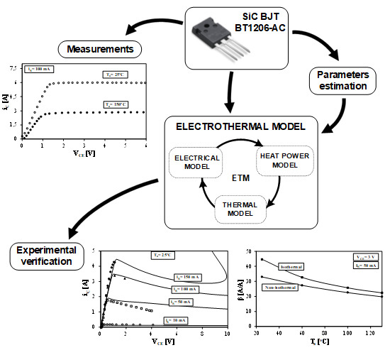
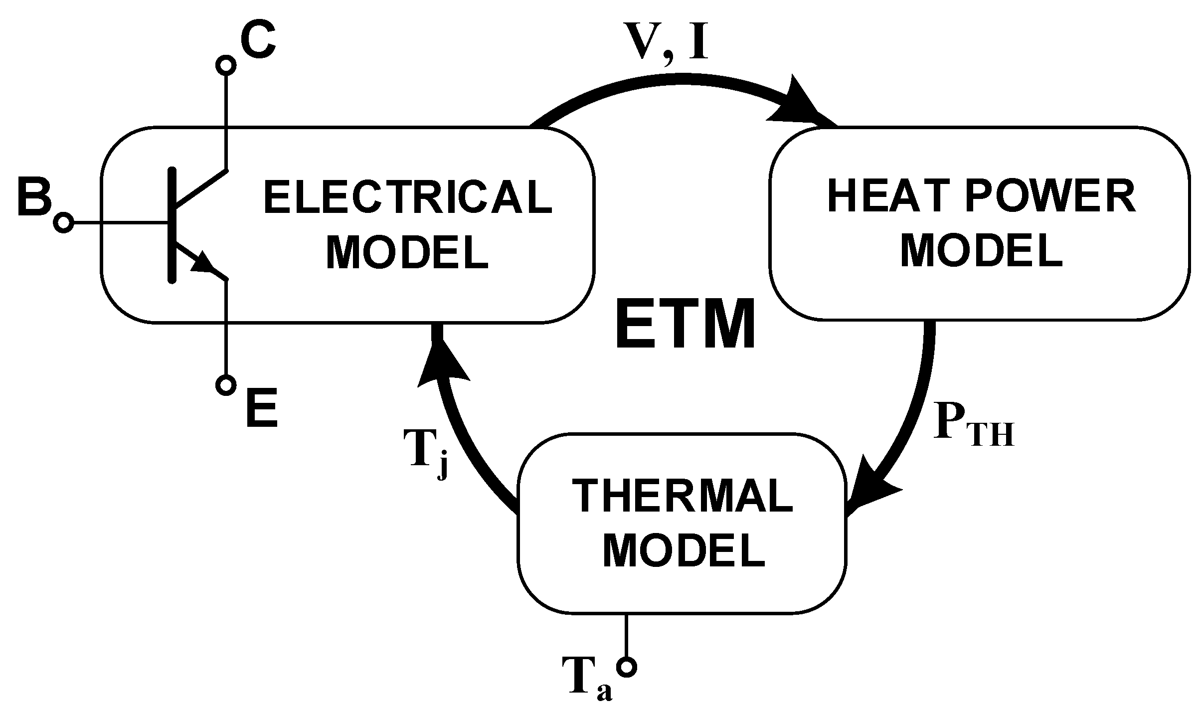
A block diagram of the electrothermal model (ETM) of SiC BJT proposed by the authors is demonstrated in
Figure 1.
As presented, the ETM contains: the electrical model, the heat power model and the thermal model. The function of the electrical model is to determine the static characteristics of the transistor for a known temperature (Tj) of its interior. The heat power model is designed to determine the value of electrical power generated in the transistor based on the currents and clamping voltages values on the transistor leads. The thermal model calculates the actual value of transistor junction (inner) temperature based on the ambient temperature (Ta) and the thermal parameters associated with the transistor cooling method.
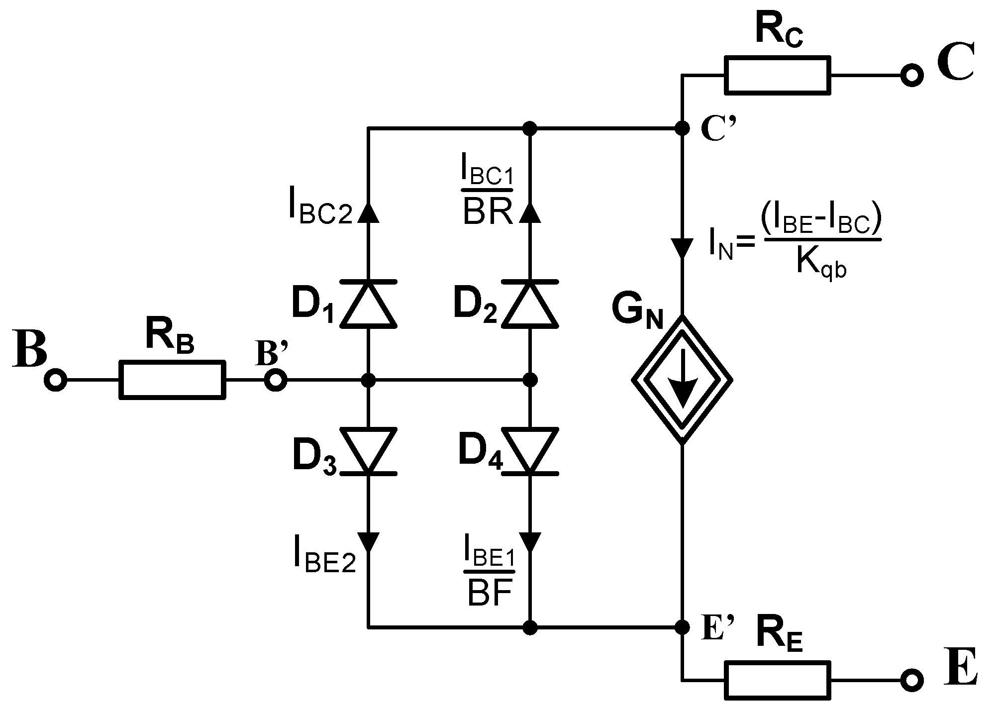
The form of the considered electrical model is based on the G–P model. However, in our model, a voltage-dependent collector resistance is used for modelling the quasi-saturation mode that starts to be visible in the higher temperature range in SiC BJTs’ static output characteristics. The quasi-saturation region model is based on the Kull model and consists of the temperature-dependent intrinsic carrier concentration model dedicated to the devices made of silicon carbide. A network form of the proposed electrical model is demonstrated in
Figure 2 [
1,
16,
19].
Diodes D
1–D
4 model the generation and recombination phenomena in the layers of the collector/emitter-base junctions, whereas D
1–D
2 and D
3–D
4 represent the ideal and non-ideal component of these junctions, respectively. Values of the collector and the base current of the transistor are of the form [
19]:
where the currents I
BE1, I
BE2, I
BC1, I
BC2 are defined as follows [
19]:
where β is the current gain factor, V
BE is the intrinsic (B’–E’) base-emitter voltage, V
BC is the intrinsic (B’–C’) base-collector voltage, IS, ISE and ISC are the saturation currents, NF and NR are the current emission coefficients, NE and NC are the leakage emission coefficients and coefficient K
qb is of the form [
19]:
where V
AF, and V
AR are early voltages, IKF and IKR are the knee current parameters, and NK is the high-current roll-off coefficient.
Efficiency of the controlled-current source G
N from
Figure 2 is of the form [
19]:
The coefficient β existing in Equations (1) and (2) are defined as [
20]:
where T
0 is the nominal temperature, β
0, α
i, γi, a, b, c, and d
1 are the model parameters.
Resistors R
E and R
B represent series resistances of the emitter and base areas according to Equation [
19]:
where TRE1, TRB1, TRE1 and TRE2 represent linear and quadratic temperature coefficients of the emitter and the base resistances, respectively.
The voltage-dependent collector resistance (R
C) dedicated for the quasi-saturation region modeling is described as [
1,
16]:
where N
epi is an epi-layer collector doping concentration, V
B’C’ and V
B’C are voltages in the selected end of the collector resistance, q is the elementary charge, and n
i is the intrinsic carrier concentration defined as [
1,
16]:
where E
g0 is SiC bandgap at zero temperature, k is Boltzmann’s constant, A is the material constant independent of temperature.
The zero-bias collector resistance R
C0 existing in Equation (12) is of the form [
1,
16]:
A detailed specification of the mathematical description of the considered model is achievable in the SPICE user manual [
19] and other papers [
1,
16,
20].
In the thermal model, the heat interactions between the device interior and the ambient temperature were taken into account. As a rule, the compact thermal model of a semiconductor device is represented by the form of the RC network. Based on this form from other works [
21,
22], the non-linear compact thermal model of the SiC BJT was demonstrated. Thermal capacitances hardly depend on the temperature in contrast to the thermal resistance that changes with the temperature. In the presented model controlled voltage sources were used only instead of R elements. The network representation of the considered model is shown in
Figure 3.
The controlled-current source GP expresses the power dissipated in the device, controlled voltage sources ER1, ER2, …, ERn express temperature changes between every part of the thermal dissipation path. The analytical form of these voltage source efficiencies takes into consideration changes in the thermal resistance value expressing the thermal dissipation between the specific construction parts. Capacitors C1–Cn describe thermal capacitances of every construction part. The voltage at nodes Tj and Ta represents the transistor junction temperature and the ambient temperature respectively.
Efficiencies of controlled-current source G
P and controlled-voltage sources are of the form [
21,
22]:
where d
i is the quotient of R
n thermal resistance and the transistor thermal resistance R
th, R
th0, R
th1, p
0 are the model parameters, and i
n is the current of the source E
Rn.
3. Results of Measurements and Simulations
To test the accuracy of the presented electrothermal model, static isothermal and non-isothermal characteristics of the BT1206-AC SiC BJT were measured and compared to the results of SPICE calculations. The model was implemented in SPICE in the form of the subcircuit. A set of electrical parameter values of the ETM was used in the simulations. The values of the model parameters were acquired from the measured characteristics with the use of the proper parameters estimation procedure described in [
20,
23]. The values of parameters occurring in Equation (15) were acquired from measurements of the transistor transient thermal impedance.
Isothermal characteristics of the selected transistor were measured by means of Keithley Source Measure Unit type 2602 in order to minimize the impact of the self-heating phenomenon on the measured characteristics of the tested device. During the measurements, a signal with a duty cycle of less than 0.0001 and a pulse duration of 50 μs was used. The non-isothermal characteristics were performed by the “point by point” measurement method for the transistor operating without any cooling system under the thermal steady-state. During the measurements, the case temperature TC of the transistor was measured by a TM-2000 precision thermometer comprising a platinum Pt-100 sensor. The temperature sensor was glued on the transistor case by a heat conductive AG Termoglue, 10 G.
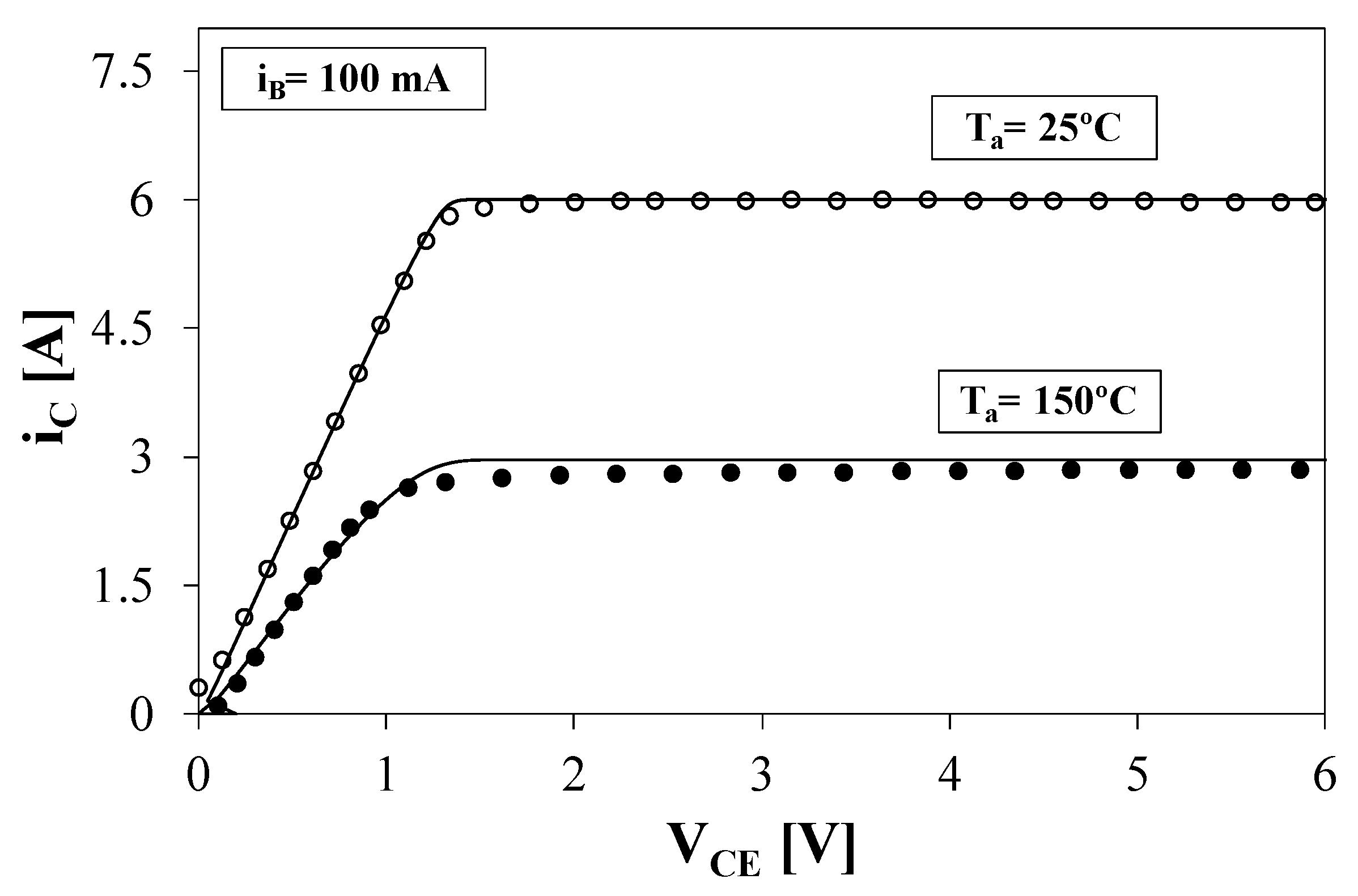
The measured and simulated isothermal static output characteristics of the BT1206-AC transistor are presented in
Figure 4, where points represent the results of measurements and lines represent the results of simulations using the proposed ETM.
As seen in
Figure 4, good agreement between the results of the isothermal measurements in comparison with the simulations was obtained even in the quasi-saturation region at both values of the ambient temperature, which expresses a percentage relative error (absolute error quotient and exact value) of less than 8%. The increase of the ambient temperature causes the collector current value drop in the bipolar silicon carbide transistors, but it is commonly known from the literature that in the case of the bipolar transistors made of silicon, this dependence is reversed [
24,
25].
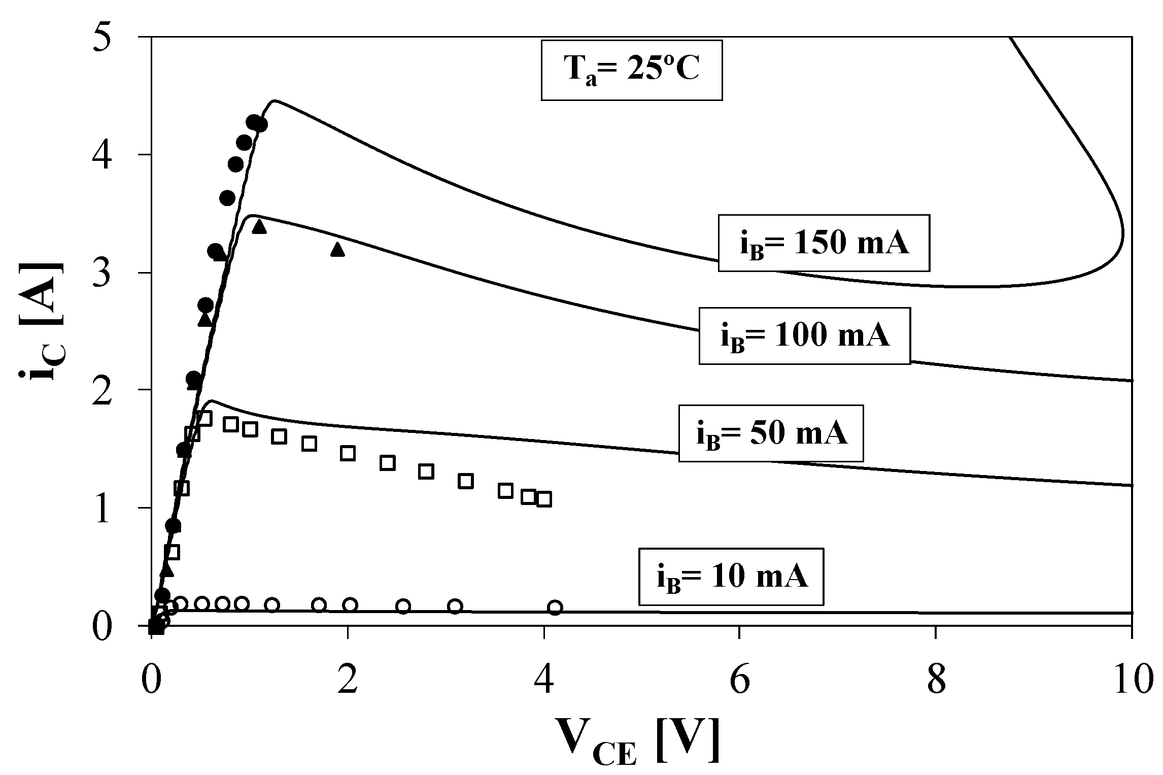
Measured and calculated non-isothermal I-V characteristics of the considered SiC BJT transistor are shown in
Figure 5. The investigations were performed at four fixed values of the control current in the range of 10–150 mA. As shown in
Figure 4 and
Figure 5, the differences between the results of isothermal and non-isothermal measurements of the static output characteristics i
C(v
CE) reach over 50% for a control current equal to i
B = 100 mA and a voltage v
CE of 4 V at room temperature.
As seen, the satisfying agreement between the results of simulations and measurements was expressed by a relative error value of usually less than 10%. The measurements were carried out to obtain the transistor junction temperature (Tj) close to the maximum value of this parameter given in the catalogue by the manufacturer. The junction temperature was estimated on the basis of case temperature (TC) measurements and catalog value of the thermal resistance Rthjc between the transistor junction and case.
The simulated output characteristic at the base current equal to 150 mA has a specific shape. The negative slope of the collector current with increasing collector-emitter voltage is caused by the strong self-heating phenomenon. In the literature, this type of characteristic is called an N-shape characteristic [
8].
The important parameter in the description of the bipolar transistors is the common-emitter current gain factor (β), defined as the ratio of the output and control current (β = I
C/I
B). It is known from the literature that the value of β depends on the operating point. In catalogs, usually only one value of this parameter is given (under set operating conditions). Manufacturers deliberately choose a specific transistor operating point to present the highest value of the current gain factor β.
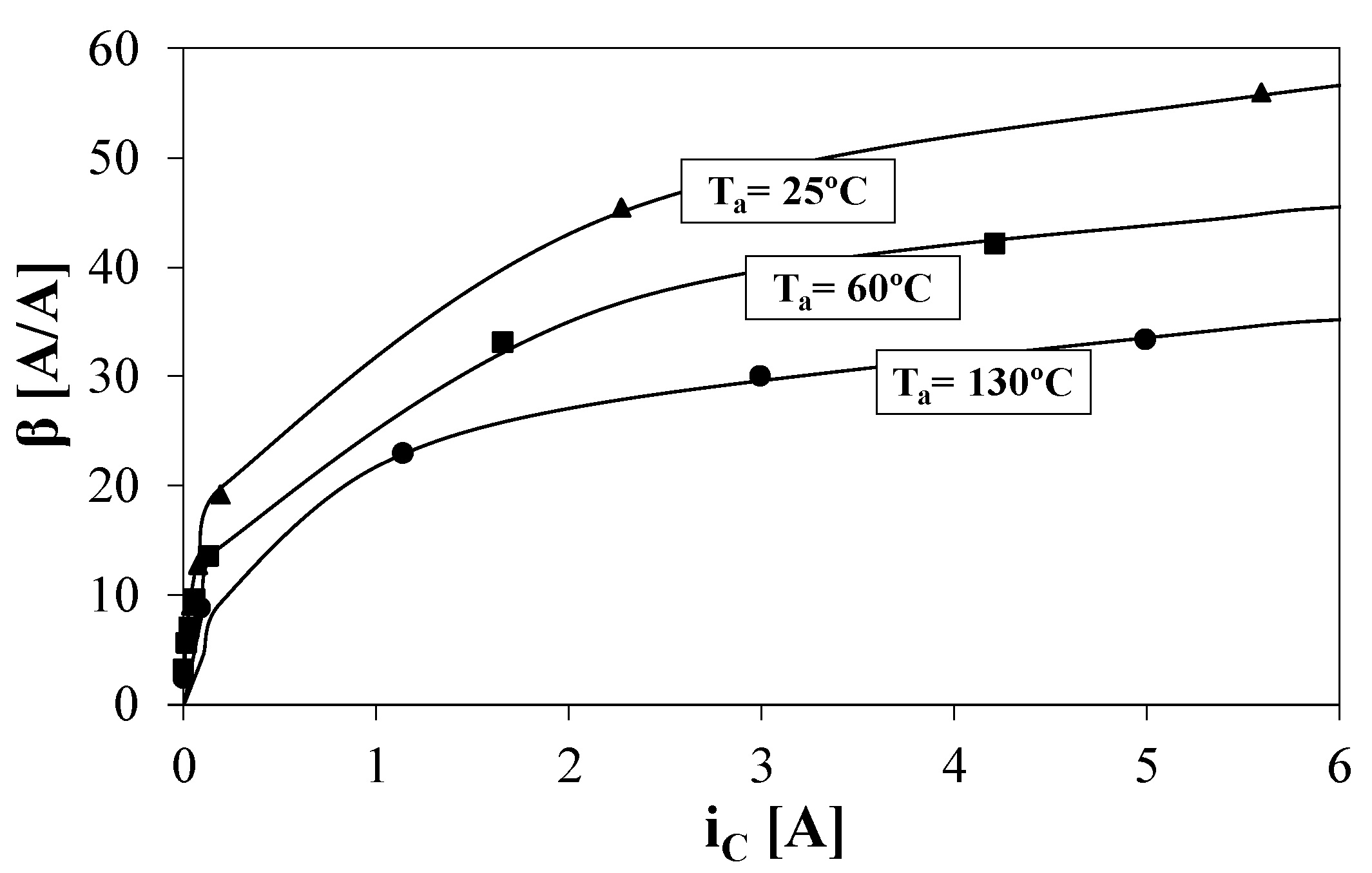
Figure 6 shows the authors’ measured and calculated values of β factor for the considered transistor in the isothermal conditions at a fixed value of the collector-emitter voltage equal to 3 V.
As seen, in the range of collector current values up to about 6 A, the β(i
C) dependence is a monotonically increasing function. In addition, the dependence of the current gain factor β(T) at a fixed value of a collector current is a decreasing function. This is a characteristic feature of bipolar power transistors made with silicon carbide technology [
8,
25,
26,
27]. The results of simulations using the proposed β model has a good agreement with the results of the measurements of the β(i
C) characteristics in all ranges of temperature, which indicates that the transistor’s current gain properties deteriorate with the temperature increase.
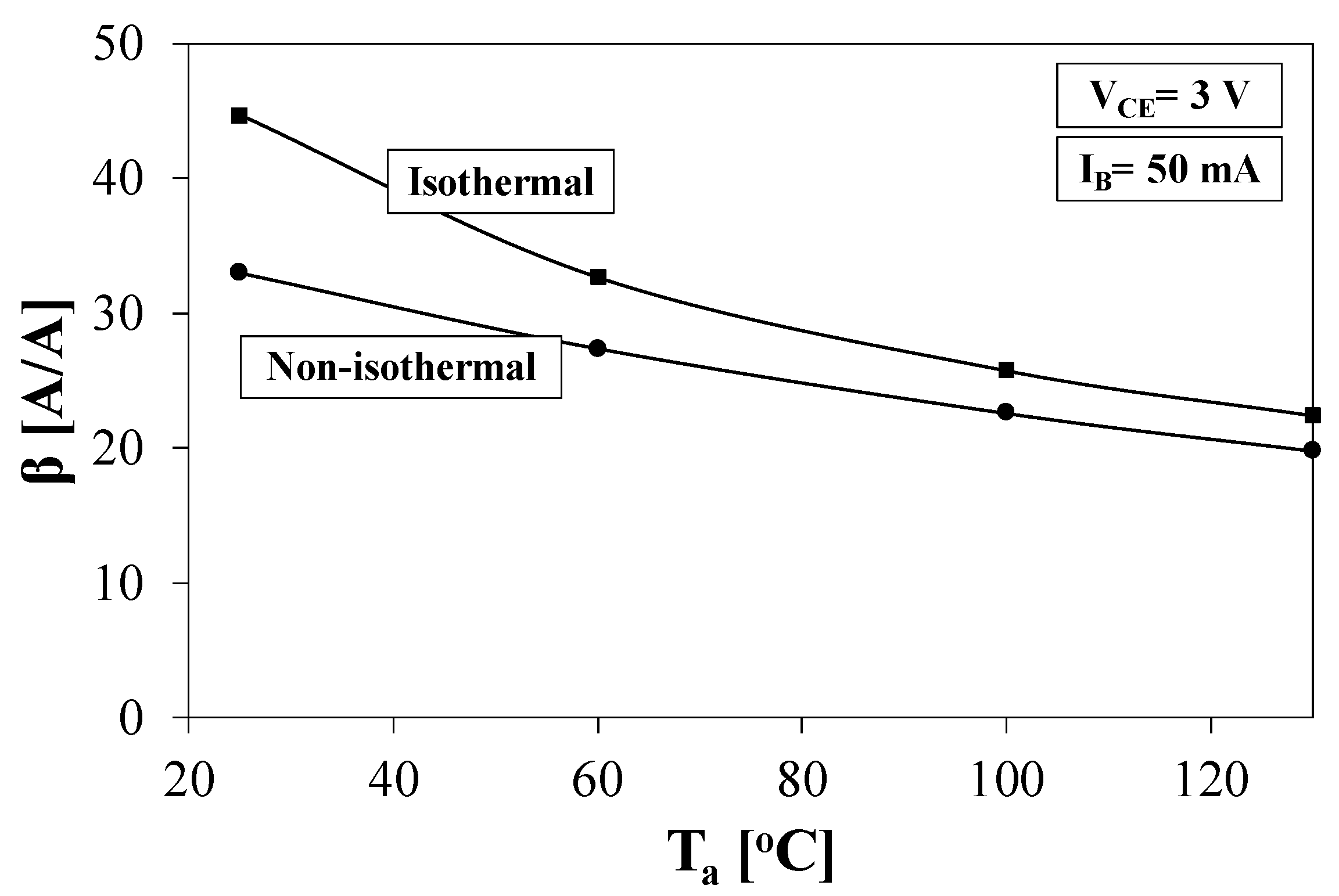
Figure 7 presents the isothermal and non-isothermal dependence of the current gain factor β of the considered transistor on the ambient temperature at a fixed value of the collector-emitter voltage and the control current equal to 3 V and 50 mA, respectively. The points represent the results of measurements and lines represent the results of calculations using the proposed ETM.
As seen, the non-isothermal characteristic of SiC BJT lies under the isothermal counterpart. Moreover, at room temperature the differences between isothermal and non-isothermal measurements reach over 25%. This phenomenon is due to the fact that when the device lattice temperature and phonon scattering in SiC BJTs increase, they cause both the carrier mobility and the current gain to drop [
28].
4. Conclusions
The authors’ measurements show that the ambient temperature rises strongly affect certain characteristics and parameters of the silicon carbide power bipolar transistor. Moreover, the self-heating phenomenon in SiC BJT can result in not only qualitative but also quantitative changing of the semiconductor device characteristics shape, resulting in the negative slope of collector current with increasing collector-emitter voltage occurrence and causes decreasing of the current gain factor β with power dissipation increase.
In the typical Gummel–Poon model implemented in SPICE, the self-heating phenomenon is not taken into account. In this paper, the authors proposed an improved SiC BJT model dedicated for SPICE, incorporating not only the self-heating phenomenon, but also modeling the quasi–saturation mode using the temperature-dependent intrinsic carrier concentration model. Apart from this, the current gain factor model is used for the first time for the bipolar transistor made of silicon carbide taking the temperature and collector current impact into account. The proposed electrothermal model of the BT1206-AC SiC BJT allows calculating the non-isothermal characteristics of the tested device. The simulated and measured characteristics of considered SiC power BJT were compared. The satisfactory agreement between both the calculated and measured characteristics indicates the correctness of the presented model. It is worth mentioning that the accuracy of the proposed model can be achieved even at high current density when the current gain factor β starts to decrease.


