Article

Design Considerations of Series-Connected Devices Based LLC Converter

Department of Electrical Engineering, Konkuk University, Seoul 05029, Korea
*
Author to whom correspondence should be addressed.
Energies 2020, 13(1), 264; https://doi.org/10.3390/en13010264
Submission received: 30 November 2019 / Revised: 31 December 2019 / Accepted: 2 January 2020 / Published: 5 January 2020
(This article belongs to the Special Issue Advances in High-Efficiency LLC Resonant Converters)

Abstract

:
This paper describes the design of a Series-Connected Device based on a fixed–frequency LLC resonant converter (SCDLLC). Isolation of the dc-dc converter like the LLC resonant converter is used for the stability of the high voltage system such as a solid-state-transformer (SST). The series-connected devices driving method is one of the methods applicable to a high voltage system. When driving series-connected devices, an auxiliary circuit for voltage balancing between series-connected devices is required, which can be simply implemented using a passive element. In this paper, LLC converter design with balancing circuits configured in parallel with a device is provided, and both the simulations and experiments were performed.

Graphical Abstract

1. Introduction

Recently, with new technologies such as smart grid and DC distribution, SST have emerged. SST connects directly to the grid instead of the traditional transformers to perform a variety of roles such as power factor correction and DC distribution. Therefore, SST should be able to cope with the high voltage of the grid, so that the various studies can be conducted [1,2,3,4,5,6,7,8]. To cope with high voltage, a multi-module converter (MMC) or a series-connected switching devices method has been studied. 
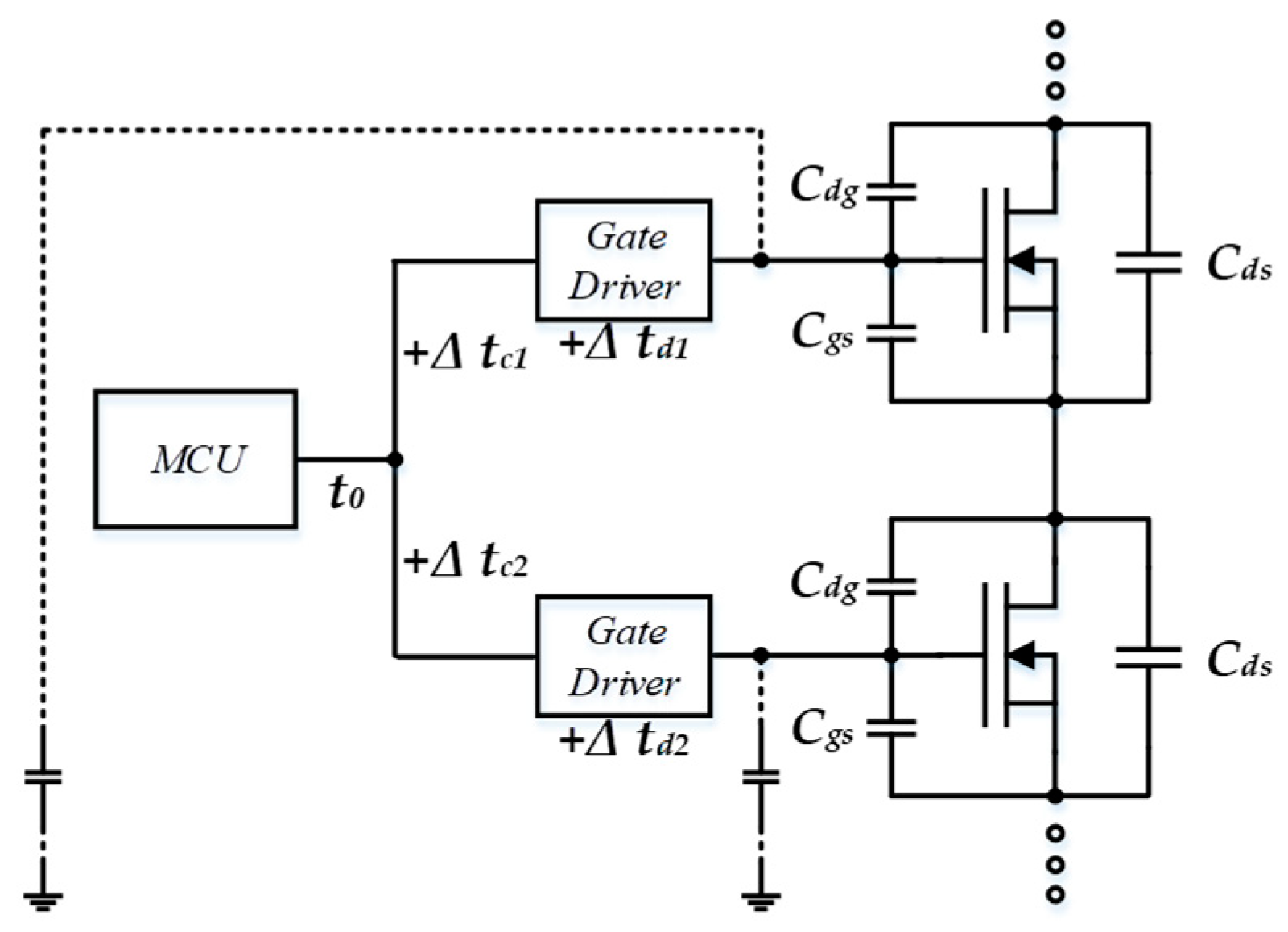
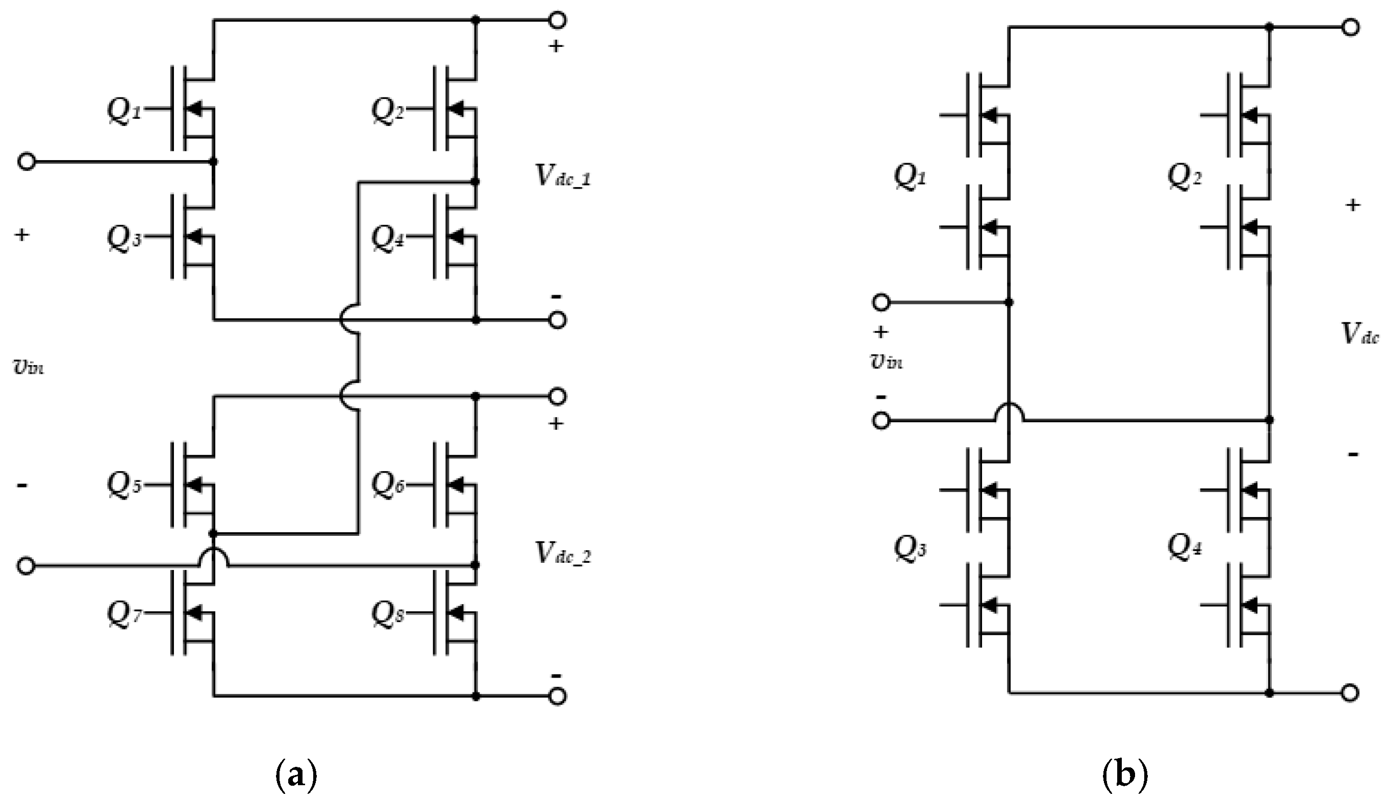
Figure 1 shows the difference between MMC and the series-connected device method.
MMC is a structure that increases the front of the circuit by stacking the circuit in series, which is relatively easy to expand, and has the advantage of reducing filter size by increasing the Power Conversion System (PCS) voltage level. But, since there is a separated DC link voltage, it is necessary to control and balance the separated DC link voltage. In addition, all individual devices should be controlled as the number of modules increases, which requires a digital computing device with many Pulse Width Modulation (PWM) channels. On the other hand, the series-connected devices behave like a single device, so even if many devices are connected in series, no digital computing device with many PWM channels is required. Furthermore, due to the series-connected devices, PCS does not have the separated DC link voltage. No additional control method is needed for DC link voltage balancing. On the other hand, because the output voltage level of series-connected devices based on PCS decreases, the filter size is larger than the MMC method. In addition, there is an issue with a switch voltage imbalance between the series-connected switches.
According to References [9,10,11,12,13,14,15,16], there are various reasons for causing a voltage imbalance. The first reason is the error of the gate driver. The gate driver is composed of various passive components and semiconductor devices like Negative, Positive, Negative (NPN) and Positive, Negative, Positive (PNP) transistors. Errors in devices of the gate driver cause an unbalance in the gate signal, which causes an imbalance in the voltage across the series-connected devices. The second reason is the error of parasitic components of the device itself. The error of the output capacitor of devices affects the switching speed and causes a voltage imbalance. The third reason is the parasitic capacitor from gate to ground of each device.
To solve voltage imbalance, various studies have been conducted [9,10,11,12,13,14,15,16]. In Reference [9], Active Gate Driver using Field Programmable Gate Array (FPGA) with RCD (Resistor, Capacitor and Diode) snubbers across each device method for balancing was proposed and tested. In the documents, the three-phase half-bridge inverter was built in 12-series connected Insulated Gage Bipolar Transistor (IGBT) and verified at a rated current within ± 10 kV DC-link. In Reference [12], an active gate driver using a current mirror with a steady-state balancing resistor was proposed and performed. The steady-state voltage imbalance is reduced by the balancing resistor, and the transient imbalance was solved by the analog gate controller used a current mirror. In Reference [14], the voltage balancing method with only passive components using a single gate driver unit was proposed. In the documents, experimental verifications were applied to the DC circuit breaker with a 1.2 kV bus voltage. It was confirmed that it is possible to cope with the high voltage system by using a series connection element applied to various methods.
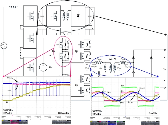
In a high voltage system, like SST, isolated converters are needed to increase the stability of the system and grid. Isolated converters are one of the necessary converters for SST regardless of MMC or series-connected devices. There are many types of isolated converters such as Dual-Active-Bridge (DAB), Quad-Active-Bridge (QAB), and LLC Converter. A fixed-frequency resonant converter conducts zero voltage switching (ZVS) over a wide frequency range and provides the advantages of high efficiency and high-power density.
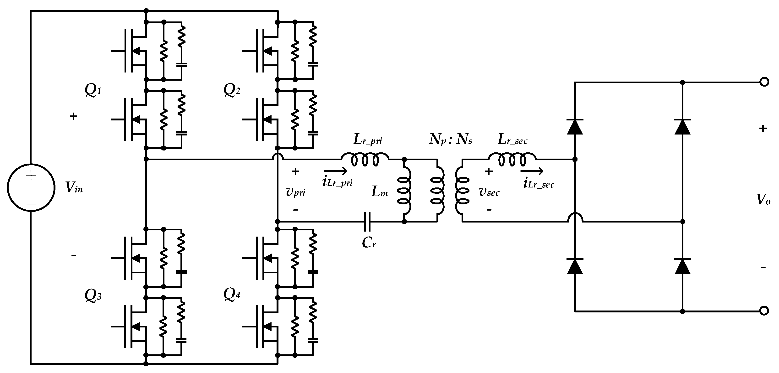
In this paper, fixed-frequency LLC resonant converter-based series-connected devices is proposed. In order to cope with a high voltage, a series-connected device based on PCS was applied and an R-C snubber was applied to solve the voltage imbalance between series-connected devices. In conclusion, this paper examined the effect of R-C snubber applied to the LLC converter to solve the voltage imbalance. The proposed converter consists of a full-bridge inverter. Unlike the usual full-bridge converter, the proposed converter consists of eight devices, as shown in Figure 1b. The operation of the SCDLLC converter with a balancing circuit is described. This paper is structured as follows. In Section 2, imbalance factors of series-connected devices are described and a balancing method using passive elements is expressed. In Section 3, a configuration method of the LLC converter considering series-connected devices is explained. In Section 4 and Section 5, a 3-kW prototype model is manufactured to verify the usefulness of the proposed system and the simulations and experiments are performed. Lastly, in Section 6, we discuss experimental results and conclude the paper.

2. Design of Series-Connected Devices Balancing Circuit

Figure 2 depicts the series-connected device with various factors that cause a voltage imbalance. Gate signal mismatch can occur due to an error of the device’s parasitic capacitor, unbalance of the gate signal due to a gate pattern, and an error of the parasitic capacitor from gate to ground, which causes an unbalance of voltage across the device. Furthermore, the voltage imbalance of devices increases the stress and can cause damage to the device. In this section, in order to prevent damage to the device, the voltage balancing method of the series-connected devices was analyzed using passive components.
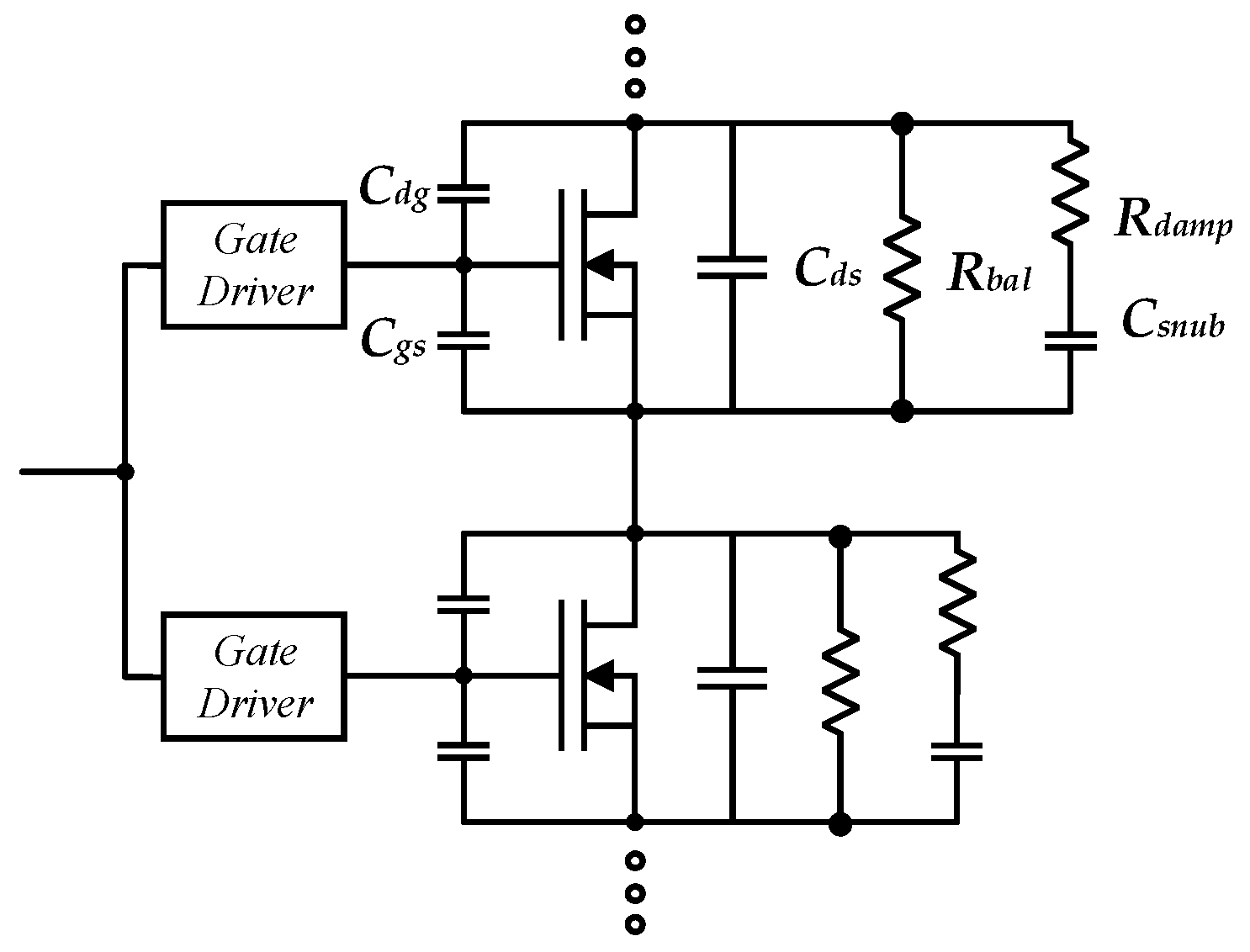
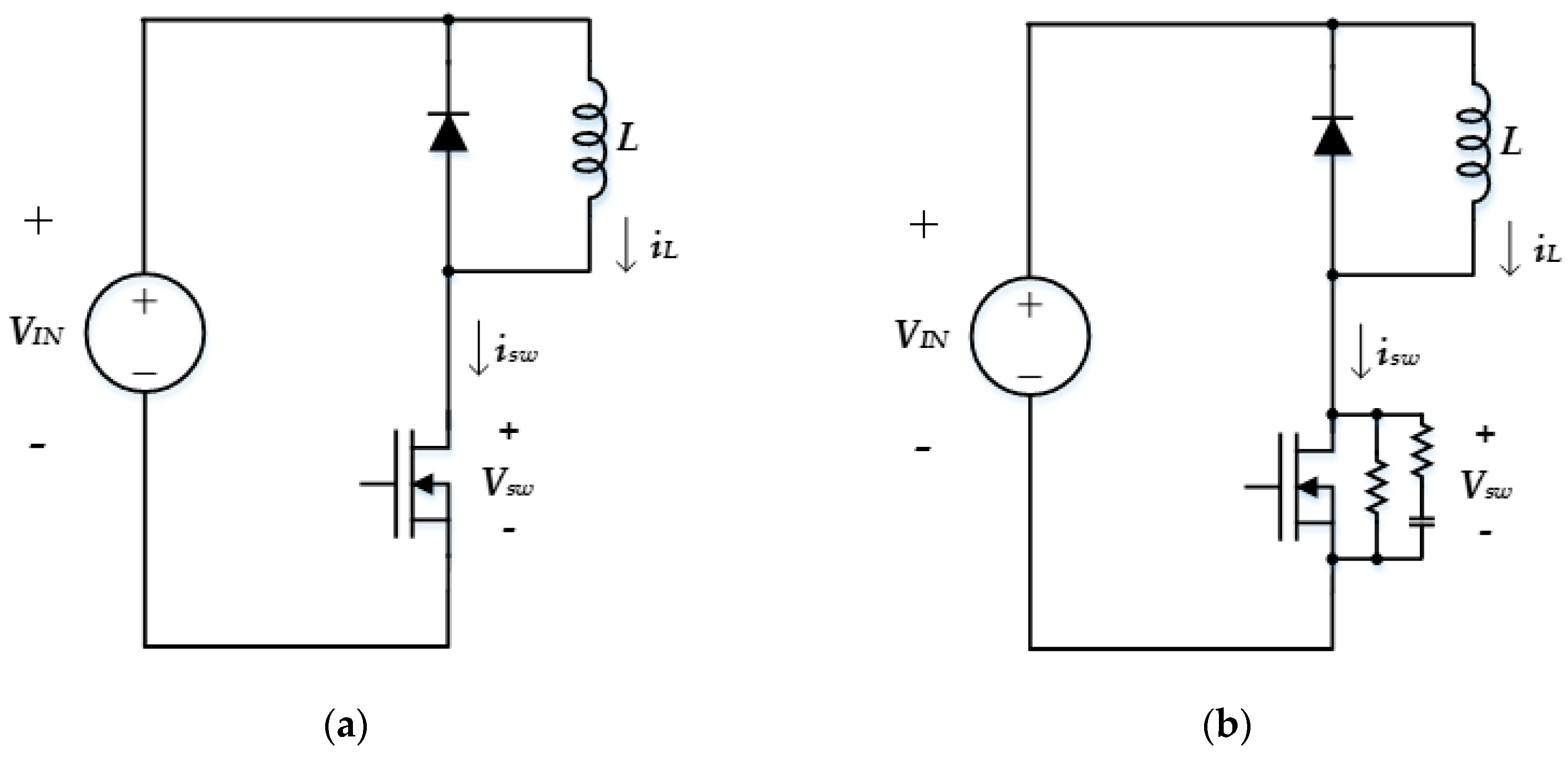
Passive snubbers implemented by passive devices (C, RC, RCD, etc.) are used for voltage balancing circuits. Voltage imbalance of devices is somewhat limited by placing the passive snubber circuit between drain to source. The use of passive snubber circuits reduces the switching speed of devices and the voltage imbalance due to a gate signal imbalance. 
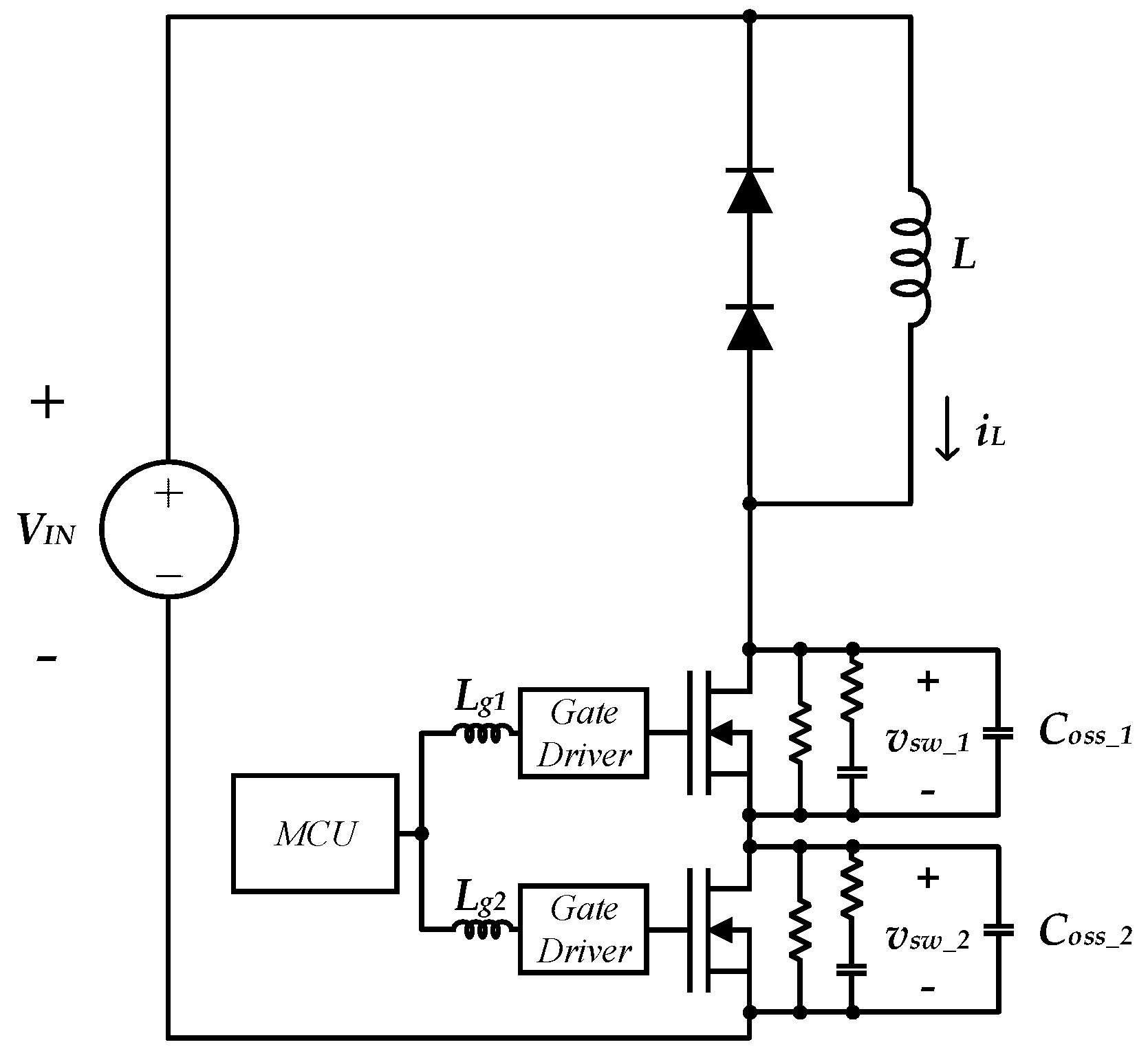
Figure 3 shows series-connected devices with passive balancing circuits. The snubber circuit composed of a steady-state balancing resistor (Rbal) and a transient state balancing capacitor (Csnub, Rdamp).
The steady-state balancing resistors operate when the switch is fully turned-off. If the steady-state balancing resistors are small, the devices are well balanced. However, the power dissipation of balancing resistors increased, which requires the use of higher-rated resistors. Conversely, If the balancing resistors are big, the power dissipation of balancing resistors decrease. However, there is a high probability that voltage balancing between series-connected devices will fail. Therefore, when designing the balancing resistor, the leakage current of the device should be considered. Steady-state resistance are calculated below.
v d s 10 × i l e a k a g e _ m a x < R b a l < v d s 10 × i l e a k a g e _ m i n
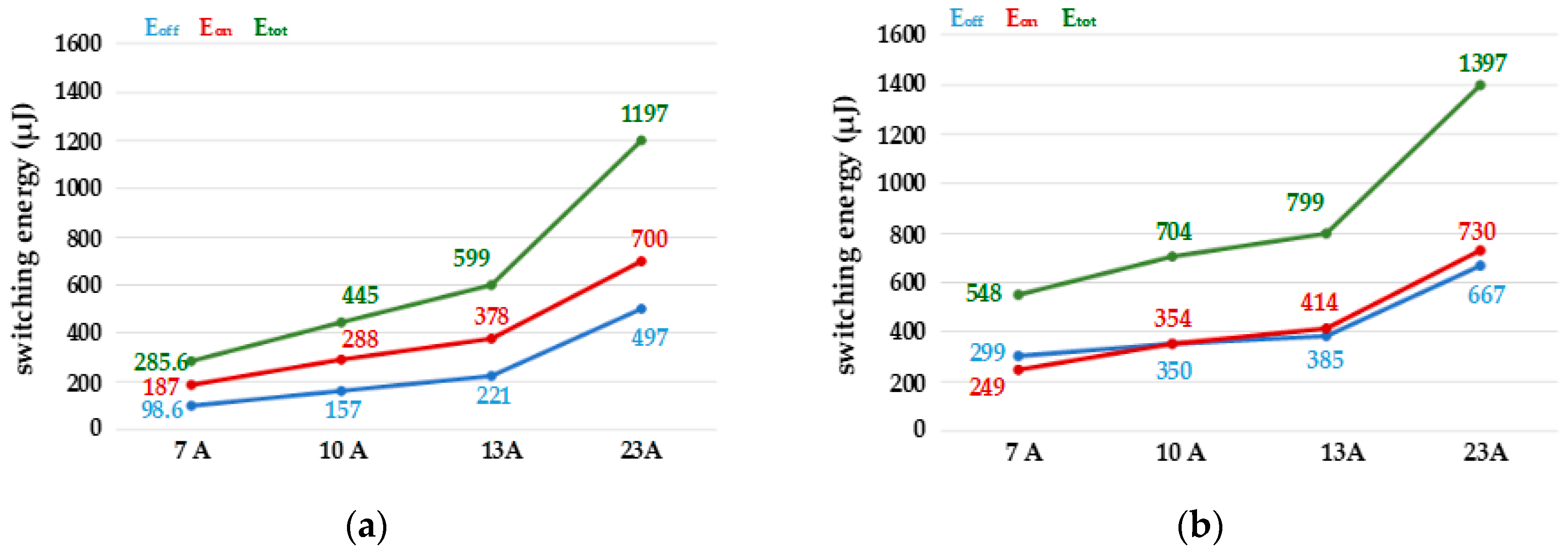
The transient state balancing circuit (Csnub, Rdamp) operates when the switch is a turn-on state and a turn-off state. Csnub is selected considering the parasitic capacitor of the device. To avoid imbalance by parasitic capacitor errors of the devices, attach a balancing capacitor with negligible parasitic capacitors of a device. If snubber capacitance is big, voltage unbalance during the transient will be stabilized, but switching speed will decrease and switching loss will increase. If the snubber capacitance is small, the snubber capacitors cannot perform proper balancing. Rsnub works as a damping resistor. The inrush current of the snubber capacitor at the switching state is limited by Rsnub. Therefore, Rsnub is selected by the current rating of the snubber capacitor. In addition, when calculating the Rsnub value, a time constant ( τ =   R C ) and switching frequency (fsw) should be considered. A large time constant reduces the switching speed, increases switching losses, and also hinders soft switching of the LLC converter.

3. Design of LLC Converter

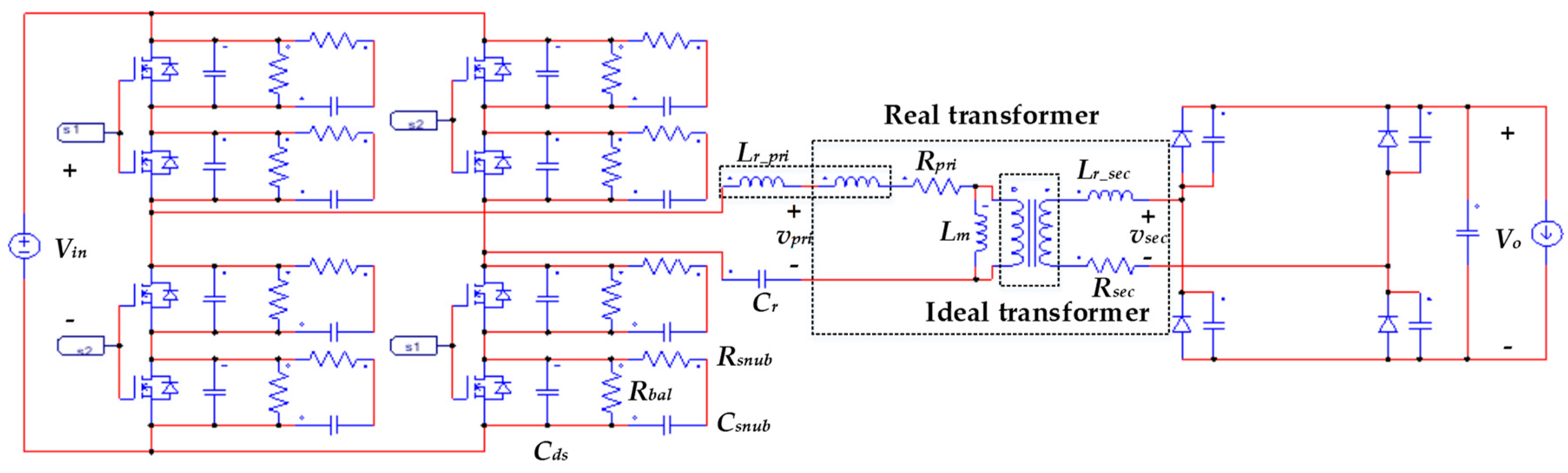
Figure 4 depicts the series-connected SiC MOSFETs LLC Converter with voltage balancing circuits. Generally, the output capacitance of the switching device should be considered in the design process. However, in this case, Snubber capacitors are added in parallel with the series-connected devices for voltage balancing. The output capacitor should be discharged during deadtime for a sufficient Zero Voltage Switching (ZVS) effect. Therefore, the snubber capacitor should be considered when designing an LLC converter. Except for the snubber capacitor, the others process of the designed LLC converter are followed by the general LLC converter design process in References [17,18].
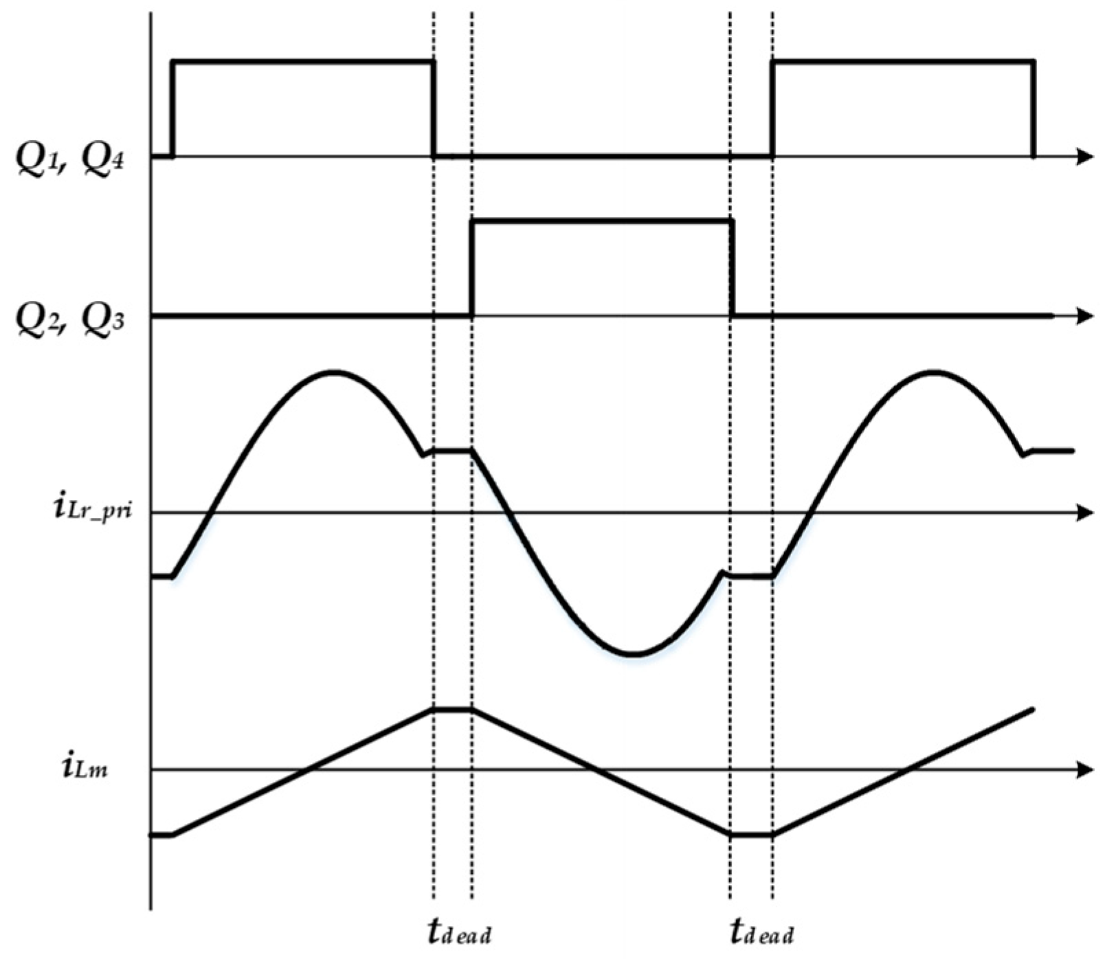
Figure 5 shows theoretical waveforms of the conventional LLC converter. For simplifying it to analyze, some assumptions are made as follows.
  • There is no error of parasitic elements of a switching device;
  • Gate drivers are all ideal, and there is no time delay between series-connected devices due to the gate driver.
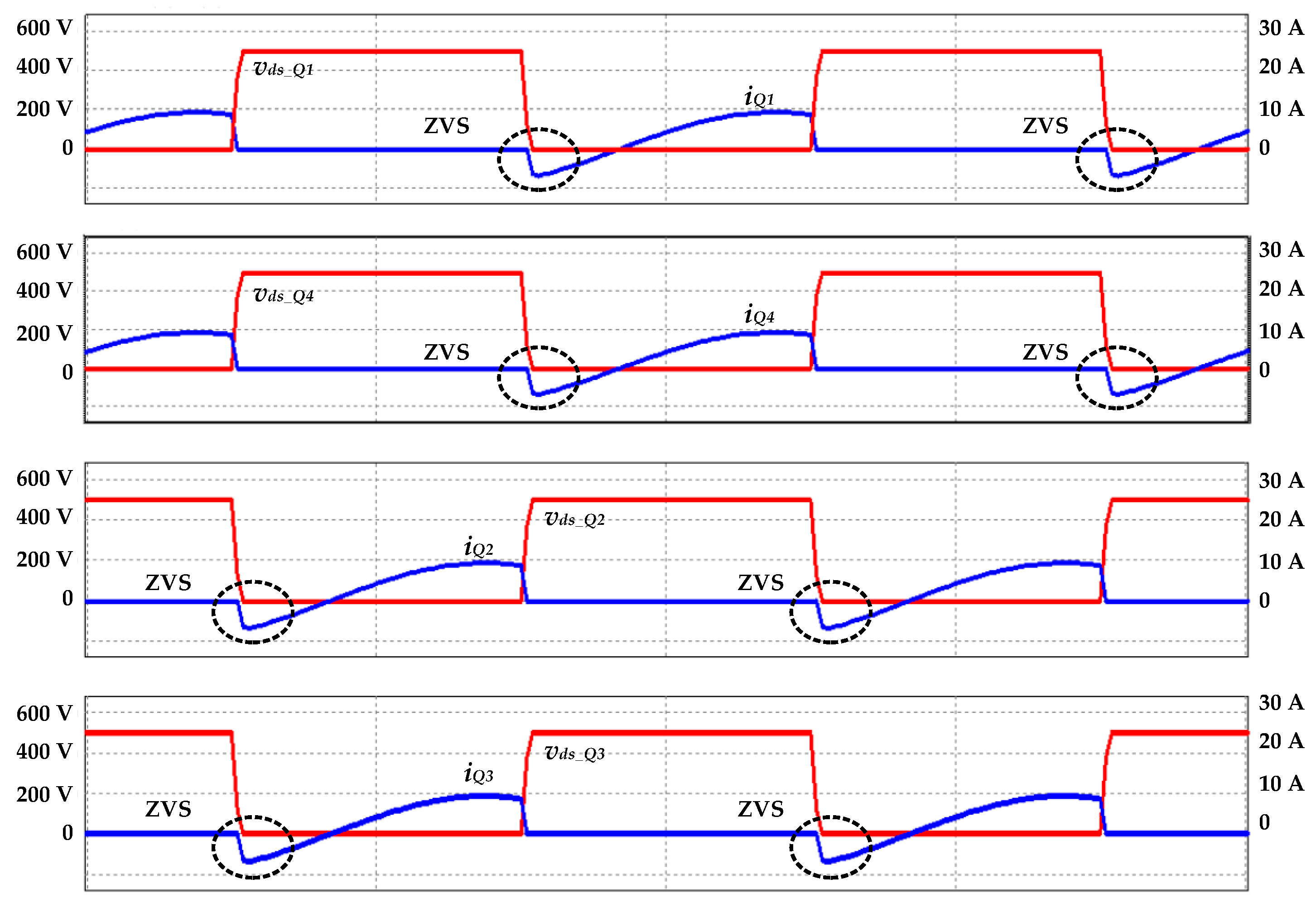
The gate signals of devices are off during the deadtime (tdead) interval. The magnetizing current and resonant current become the same during the deadtime. During the deadtime, inductor current flows through the antiparallel diode of the switch and discharges the parasitic output capacitor of the switch. Then, the switch turns on after zero voltage is formed by the discharged output capacitor so that soft switching is possible. The equation of minimum deadtime and magnetizing inductance for soft switching is calculated below.
t d e a d 16 C o s s f s w L m
Equation (2) represents that the ZVS is related to the magnetizing inductance of the high frequency transformer (HF transformer) and the output capacitance of the switch. As mentioned in the previous section, Snubber capacitors are required for voltage balance between series-connected devices. Therefore, when manufacturing the LLC converter with balancing circuits that are connected in parallel to each device, balancing circuits should be considered. This is not a parasitic component of the switch. After that, the rest process design of an LLC converter follows the conventional design process.
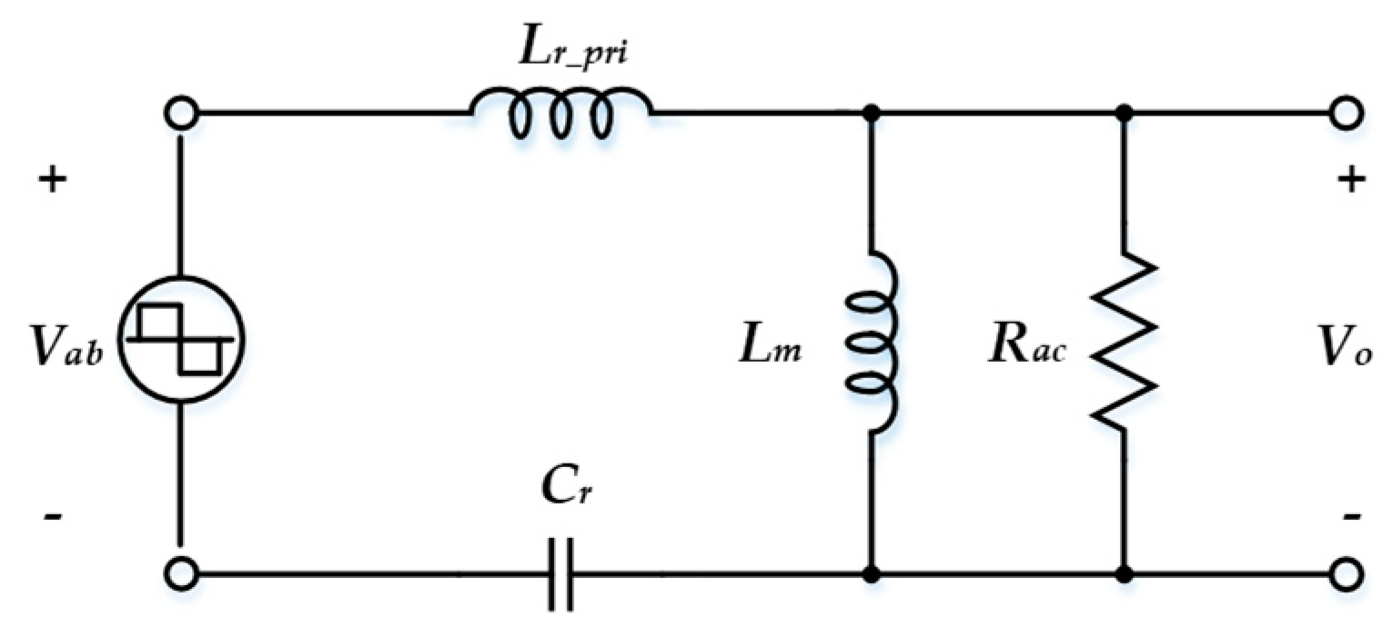
Figure 6 shows the equivalent circuit of an LLC converter. To design LLC, the converter is described as follows [3,4,5,6,7,8,9].
n   =   N p N s
m   =   L r + L m L r
f r   =   1 2 π L r C r
F x   =   f s w f r
R a c ,   m i n   =   8 π 2 · N p 2 N s 2 · R o
Q m a x   =   L r / C r R a c , m i n
where Np and Ns means the turn ratio of the transformer and Ro is the load resistance. Furthermore, fsw is the switching frequency, fr is the resonant frequency, and the Rac is the reflected load resistance. Therefore, the voltage gain of the resonant tank is defined below.
K =   | V o _ a c ( s ) V i n a c ( s ) |   =   F x 2 ( m 1 ) ( m · F x 2 1 ) 2 + F x 2 ( F x 2 1 ) 2 ( m 1 ) 2 Q 2
where Vo_ac (s), Vin_ac (s), Q, m, and Fx are the vin_ac, vo_ac, the quality factor, the ratio of the total primary inductance to resonant inductance, and the normalized switching frequency, respectively. 
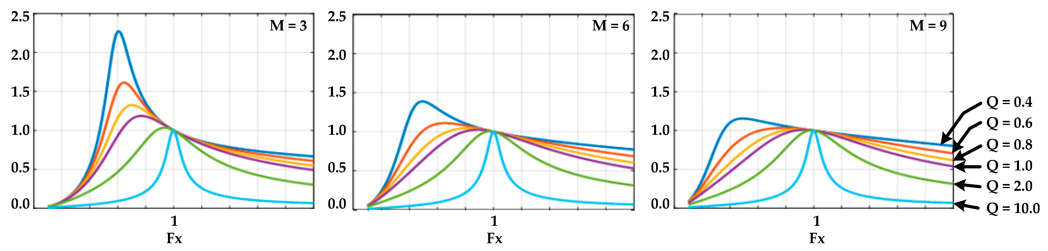
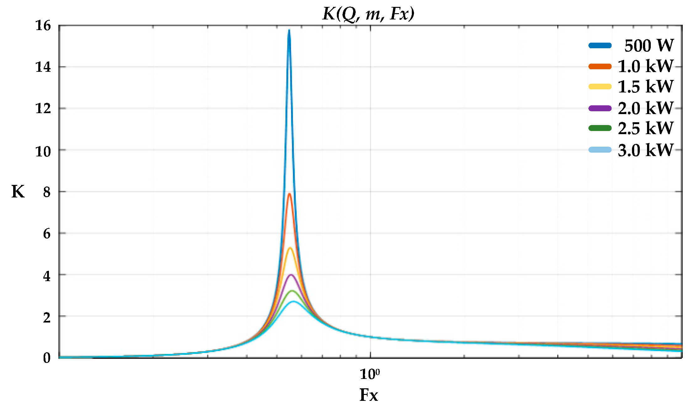
Figure 7 shows voltage gain according to different m and Q factors. In the figure, as the m factor decreases, the voltage conversion ratio is extended. However, according to Equation (4), a low m factor requires low magnetizing inductance Lm. Thus, magnetizing current increases. It means that the conduction loss of magnetic components is increased. In terms of the Q factor, the Q factor is related to the load. The high Q value means heavy load conditions and the low Q value means light load conditions. Therefore, it is important to set the Q value at the rated load. Thus, a voltage gain of an LLC converter is related to m and Q factors.

4. Simulations and Simulation Results

In order to verify the series-connected devices-based LLC converter, simulation was conducted by Power Sim (PSIM) and Linear Technology spice (LTspice).

4.1. Voltage Balancing Simulation

Figure 8 shows the simulation circuit of voltage balancing. Table 1 shows the parasitic value of components of experiment setup and Table 2 shows the parasitic value of device itself. Voltage balancing simulation was performed by LTspice. Parasitic values of devices were added arbitrarily, and voltage balancing simulation was performed depending on whether the snubber circuit was used.
Figure 9 shows the simulation results with and without balancing circuits. Without balancing circuits, simulation results show that the voltage balancing between series devices did not converge, and the voltage imbalance increased as the inductor current increased. On the other hand, with balancing circuits, voltage imbalance is somewhat reduced, and the imbalance range is maintained even with the increased inductor current.

4.2. LLC Converter Simulation

The LLC converter simulation was conducted on the assumption that voltage imbalance did not occur. The simulation model is shown in Figure 10. Table 3 gives the parameters of the system. An isolated HF transformer can be described as an ideal transformer, magnetizing inductance, and leakage inductance in simulation. In Figure 10, the model of the HF transformer of the LLC converter consists of magnetizing leakage inductance and an ideal transformer, which has a 10:4 transfer ratio. Lm means the magnetizing inductance of the fabricated HF transformer. Lr_sec means the secondary side leakage inductance of the HF transformer. Lr_pri means the primary side leakage inductance of the HF transformer, which is the sum of the leakage inductance of the HF transformer itself and the added inductance on the outside. In addition, Cr means the resonant capacitor. Resonant capacitors work as a resonant tank with Lr_pri. Therefore, the resonant frequency of the LLC converter is determined by the resonant capacitor and the primary leakage inductance of the transformer. Figure 11 shows the voltage gain curve according to the load of the proposed converter.
Figure 12 and Figure 13 show the simulation results of the LLC converter. Figure 12 shows the switching voltage and channel current of the MOSFETs. In the figure, vds_Q1, vds_Q2, vds_Q3, and vds_Q4 represents the drain to source voltages and iQ1, iQ2, iQ3, and iQ4 represents the current of devices. In the figure, the channel currents increase after the devices are fully turned on. It means ZVS is achieved. Figure 13 shows the input/output voltage and the current of the HF transformer.

5. Experiments and Experimental Results

The proposed circuit verified by simulation was tested through experiments. Figure 14 shows the experimental configuration of the proposed LLC converter using a 1200-V SiC MOSFET (C2M0040120D, Cree) and 1200-V SiC Schottky Diode (C4D20120D, Cree). Experimental specifications are shown in Table 3. Before the verification of series-connected devices based on an LLC converter, a multi-pulse test is conducted to verify voltage balancing between series-connected devices.

5.1. Voltage Balancing Experiment

Voltage imbalance was tested through a multi-pulse test. The experimental setup is shown in Figure 8. The experiment parameters are represented in Table 1.
Figure 15 shows the experimental results without balancing circuits and with balancing circuits. Compared with the simulation results, the trend tends to be different. In the simulation, the factor of voltage imbalance reflects the unbalance of the device’s parasitic and the delay of the gate signal. However, according to Reference [12], the parasitic capacitor from gate to ground one of the important factors contribute to a voltage imbalance. In addition, this factor was not reflected in the simulation. Although practical experiments, with the parasitic capacitors considered from gate to ground, the voltage imbalance converges to a steady state through snubber circuits selected by simulation. It means that, if the unbalance voltage does not exceed the rated voltage of the switch, the switch can be regarded as a stable operation with selected balancing circuits by simulation.

5.2. Double Pulse Test

As mentioned in the previous section, an added snubber circuit for voltage balancing slows down switching speed and increases switching loss. In this section, a Double Pulse Test (DPT) was conducted to analyze switching losses with and without snubber circuits. The experimental setup is shown in Figure 16 and parameters are shown in Table 4. Balancing snubber parameters are shown in Table 1.
DPT was conducted when the DC-link is 500 V. Figure 17 shows DPT results. According to Figure 17, both turn-on and turn-off losses increased with snubber circuits. However, the proposed LLC converter operates ZVS turn-on at all loads. The turn-on loss can be negligible.

5.3. LLC Converter Experiment

Based on the balancing circuit’s value selected through simulations and a multi-pulse test, the series-connected devices based on the LLC converter experiment was conducted. Figure 18 shows the main waveforms of the proposed LLC converter according to the load. In the figure, vpri and vsec represent input/output voltage of the HF transformer, iLr_pri and iLr_sec represent input/output current of the HF transformer, according to the load. As shown in the previous section, experimental results were well matched with simulation results.
Figure 19 shows vqs_1, vqs_2, and vgs at the rated power. vqs_1, vqs_2 represent the drain to source voltage of each device connected in series at the rated power. Voltage balancing between series-connected devices did not diverge, and both switches connected in series had achieved ZVS operation. Figure 20 shows the efficiency of series-connected devices-based LLC converter. The maximum efficiency was measured at the rated load.

6. Conclusions

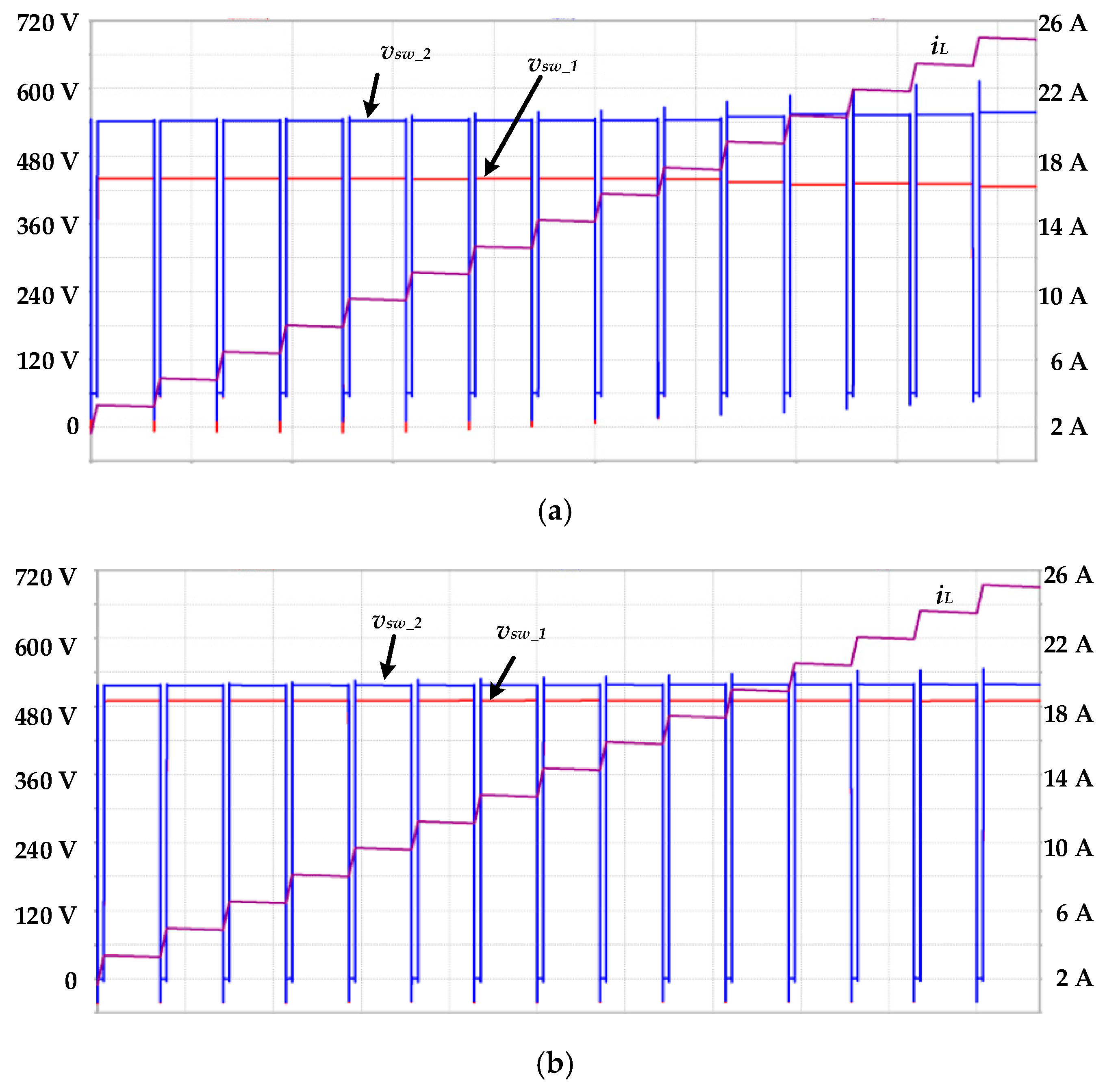
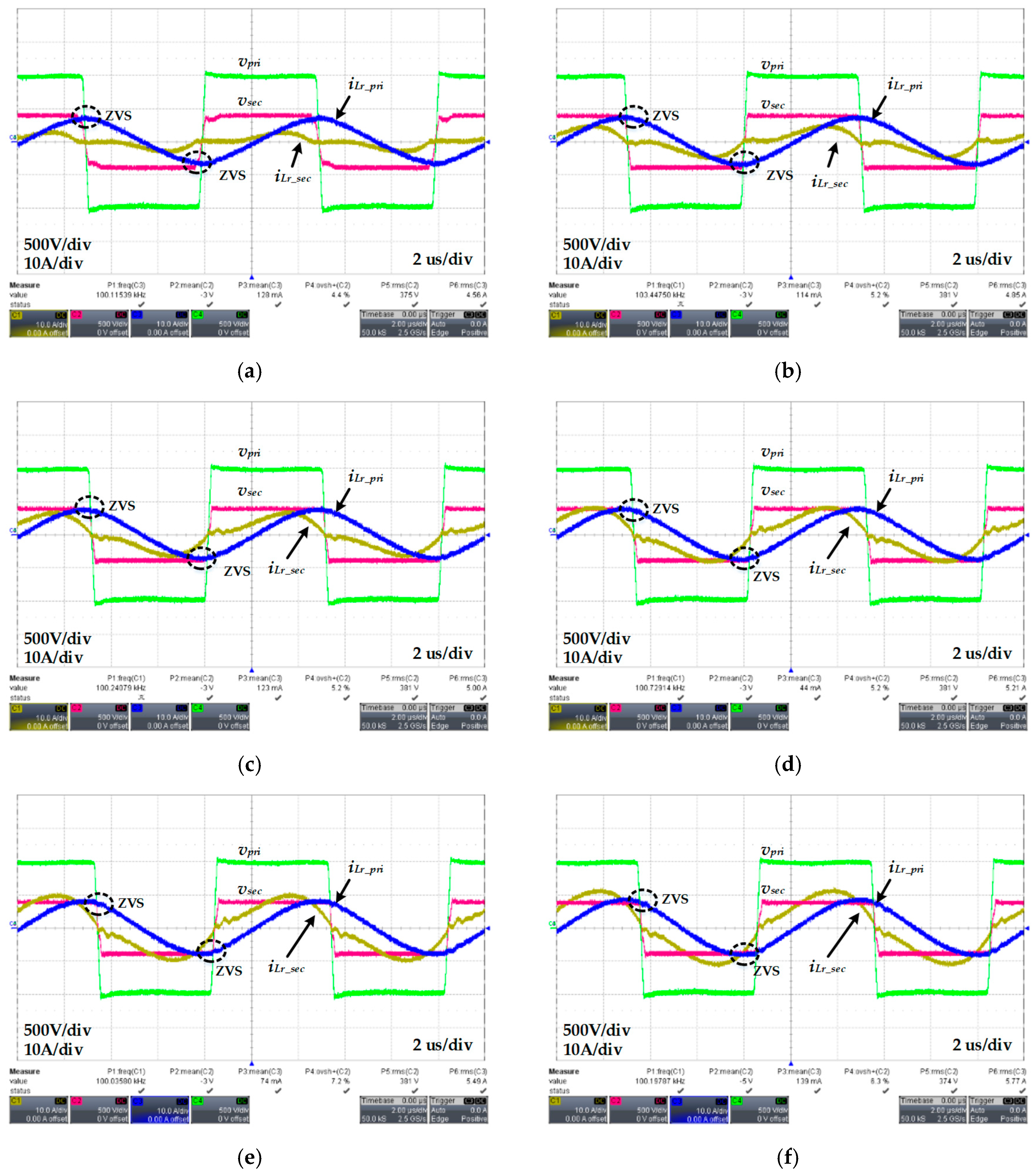
This paper describes the design consideration of the fixed frequency LLC converter considered balancing circuit of series-connected devices circuit. In the introduction, the reason for the imbalance voltage across the series-connected devices was described and discussed the need of an LLC converter. The proposed converter consists of a series-connected devices-based LLC converter.
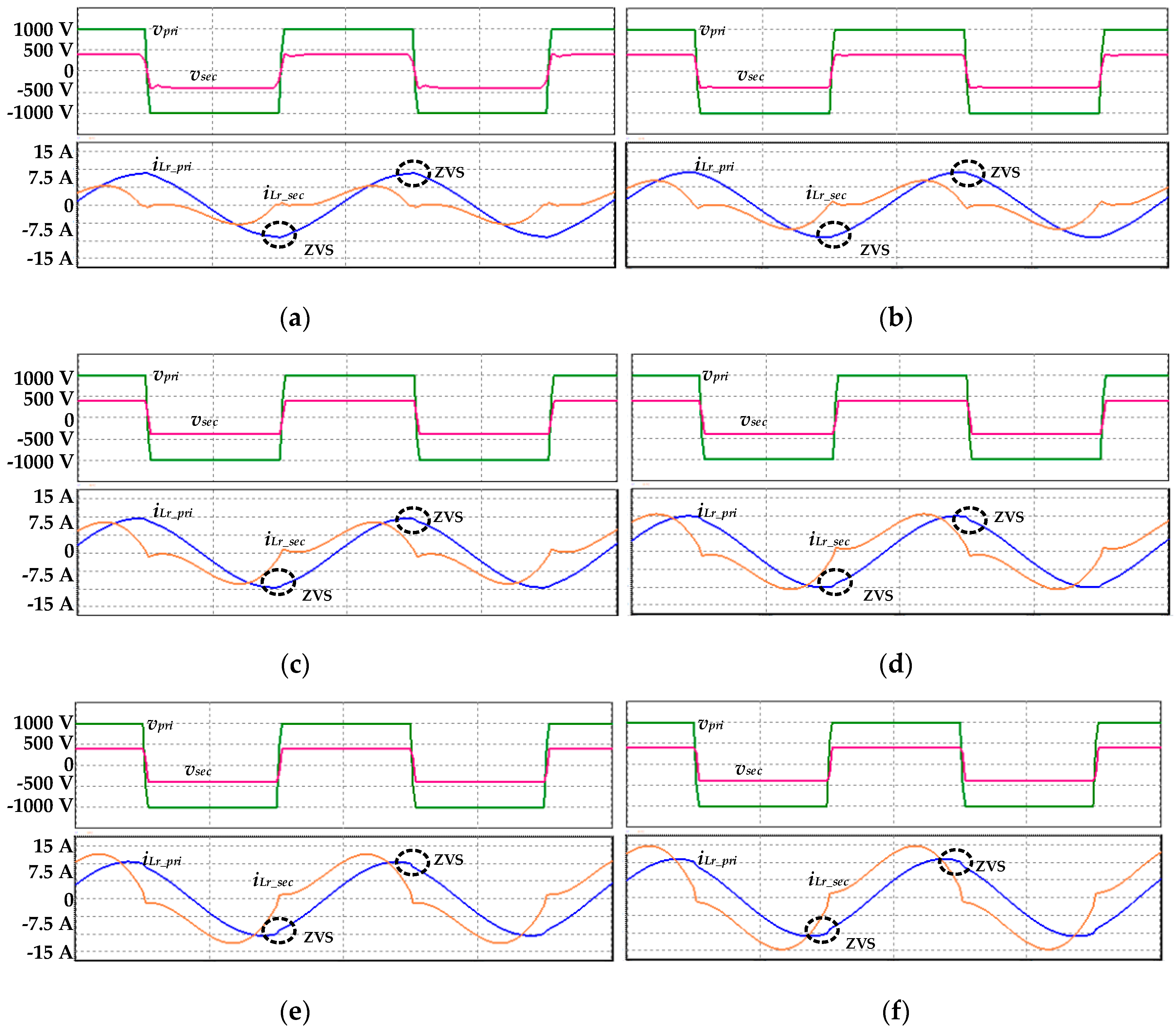
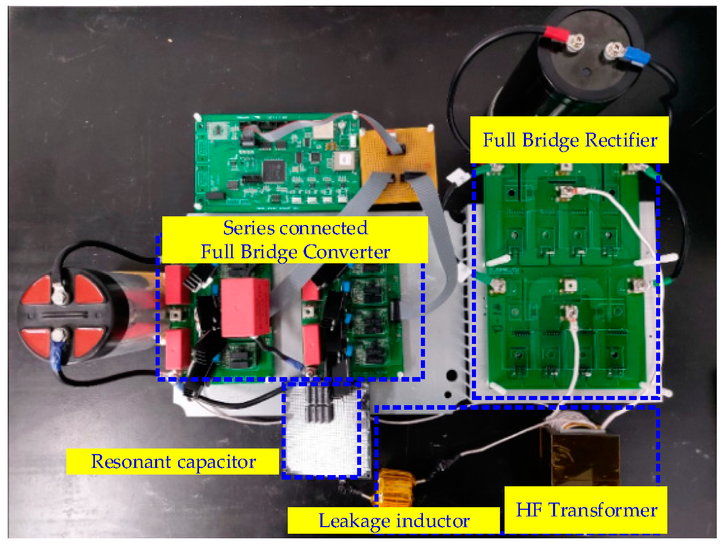
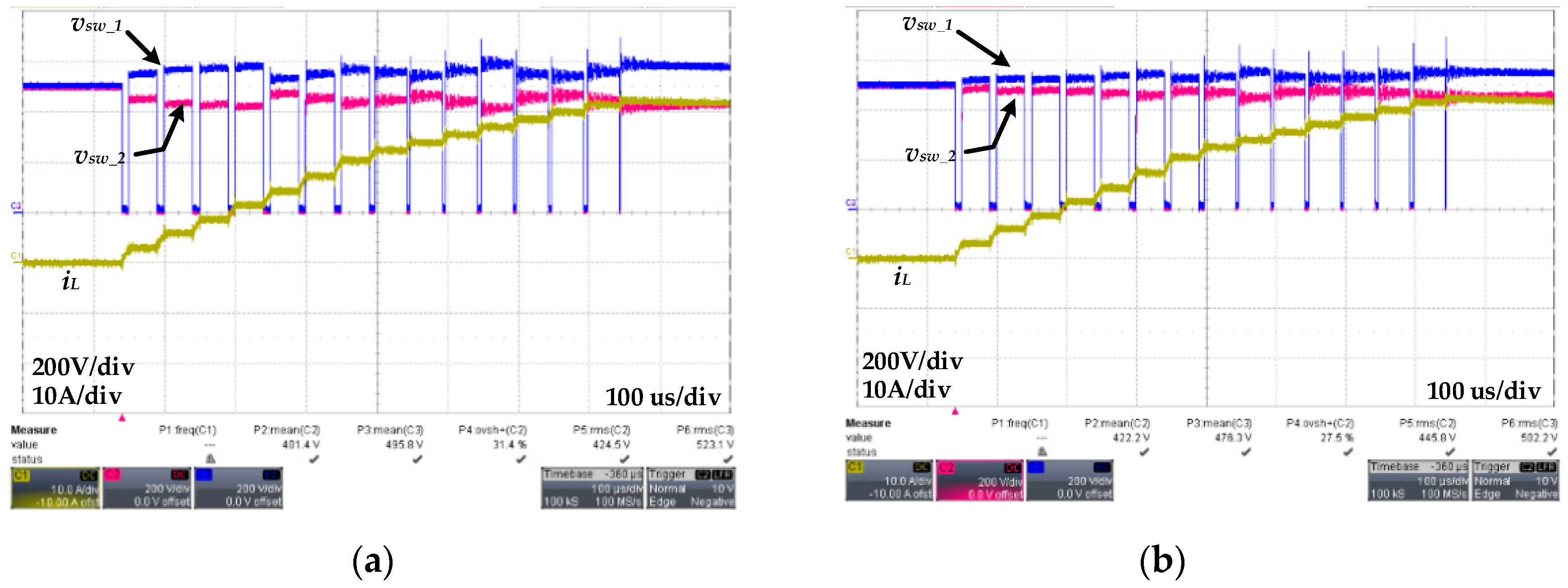
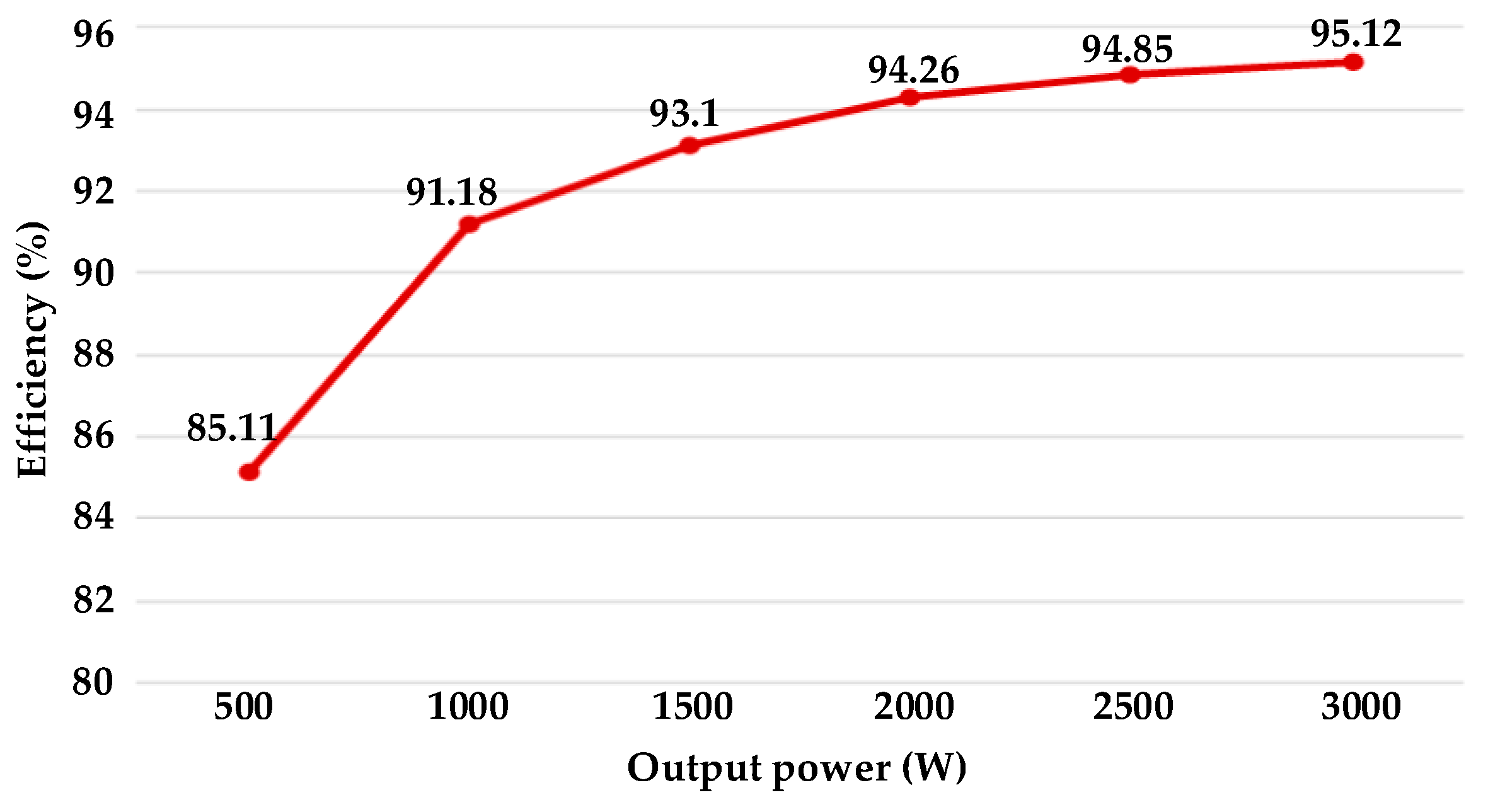
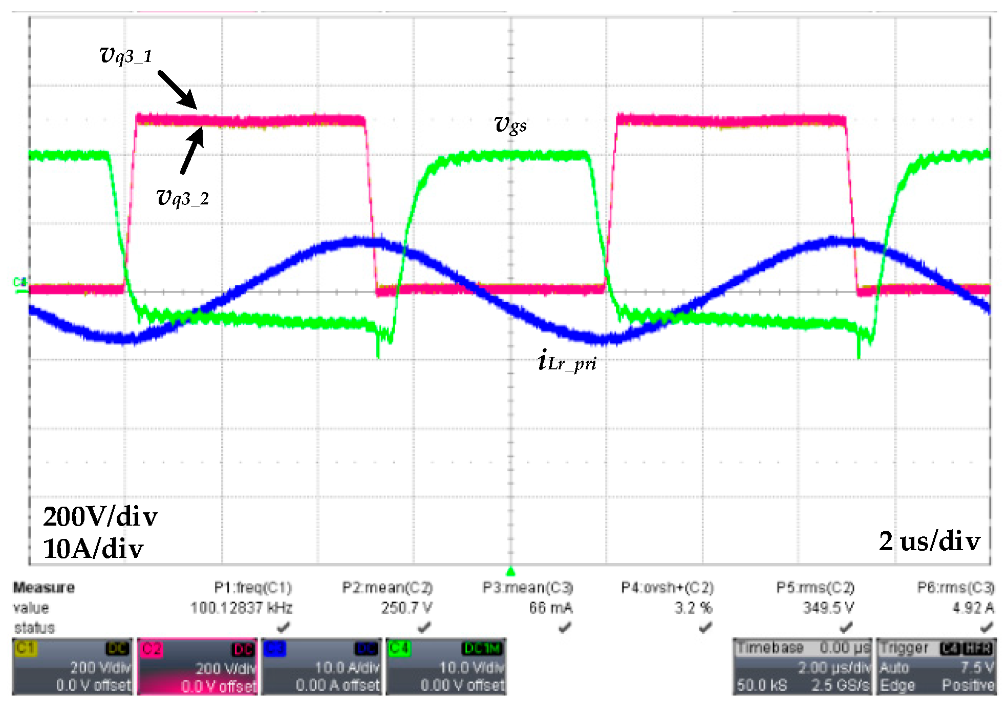
In order to verify the proposed converter, a series-connected devices-based voltage balancing experiment and the series-connected devices-based LLC converter was performed. The snubber circuit, which is the simplest method among the various methods for voltage balancing, was applied and the switching loss comparison and voltage balancing test was performed according to snubber circuits. Furthermore, based on the snubber circuits-designed simulation and experiments, 3 kW series-connected devices-based LLC converter was fabricated and verified. Through the experiments, the voltage balancing between series-connected devices and soft switching operation of the proposed converter are verified. The efficiency of a fabricated converter was measured 95.12% at 3 kW load. When the series-connected based LLC converter is fabricated with balancing snubber circuits, it is confirmed that the LLC converter design is necessary considering the balancing snubber, and the experimental results confirm that the consideration is valid.

Author Contributions

D.Y. implemented the system and conducted the experiments. Y.C. managed the paper. S.L. assisted the idea simulation and the paper writing. All authors have read and agreed to the published version of the manuscript.

Funding

The Human Resources Program in Energy Technology of the Korea Institute of Energy Technology Evaluation and Planning (KETEP) supported this work, which granted a financial resource from the Ministry of Trade, Industry & Energy, Republic of Korea. (NO. 20194030202370) and the Human Resources Program in Energy Technology of the Korea Institute of Energy Technology Evaluation and Planning (KETEP) granted financial resource from the Ministry of Trade, Industry & Energy, Republic of Korea. (Grant No. 20174010201540).

Conflicts of Interest

The authors declare no conflict of interest.

References

  1. Falcones, S.; Ayyanar, R.; Mao, X. A DC–DC Multiport-Converter-Based Solid-State Transformer Integrating Distributed Generation and Storage. IEEE Trans. Power Electron. 2013, 28, 2192–2203. [Google Scholar] [CrossRef]
  2. Fan, H.; Li, H. High-Frequency Transformer Isolated Bidirectional DC–DC Converter Modules with High Efficiency Over Wide Load Range for 20 kVA Solid-State Transformer. IEEE Trans. Power Electron. 2011, 26, 3599–3608. [Google Scholar] [CrossRef]
  3. Huang, A.Q. Medium-Voltage Solid-State Transformer: Technology for a Smarter and Resilient Grid. IEEE Ind. Electron. Mag. 2016, 10, 29–42. [Google Scholar] [CrossRef]
  4. Madhusoodhanan, S.; Tripathi, A.; Patel, D.; Mainali, K.; Kadavelugu, A.; Hazra, S.; Bhattacharya, S.; Hatua, K. Solid-State Transformer and MV Grid Tie Applications Enabled by 15 kV SiC IGBTs and 10 kV SiC MOSFETs Based Multilevel Converters. IEEE Trans. Ind. Appl. 2015, 51, 3343–3360. [Google Scholar] [CrossRef]
  5. She, X.; Huang, A.Q.; Wang, G. 3-D Space Modulation with Voltage Balancing Capability for a Cascaded Seven-Level Converter in a Solid-State Transformer. IEEE Trans. Power Electron. 2011, 26, 3778–3789. [Google Scholar] [CrossRef]
  6. She, X.; Yu, X.; Wang, F.; Huang, A.Q. Design and Demonstration of a 3.6-kV–120-V/10-kVA Solid-State Transformer for Smart Grid Application. IEEE Trans. Power Electron. 2014, 29, 3982–3996. [Google Scholar] [CrossRef]
  7. Shi, J.; Gou, W.; Yuan, H.; Zhao, T.; Huang, A.Q. Research on voltage and power balance control for cascaded modular solid-state transformer. IEEE Trans. Power Electron. 2011, 26, 1154–1166. [Google Scholar] [CrossRef]
  8. Zhao, T.; Wang, G.; Bhattacharya, S.; Huang, A.Q. Voltage and Power Balance Control for a Cascaded H-Bridge Converter-Based Solid-State Transformer. IEEE Trans. Power Electron. 2013, 28, 1523–1532. [Google Scholar] [CrossRef]
  9. Hou, K.; Zheng, Y.; Wang, X.; W, L.I.; He, A.; Jiang, Y. Practical Research on VSC Prototype Based on IGBTs Serial Connected Technology. IEEE Trans. Power Electron. 2019, 34, 495–502. [Google Scholar] [CrossRef]
  10. Ji, S.; Wang, F.; Tolbert, L.M.; Lu, T.; Zhao, Z.; Yu, H. An FPGA-Based Voltage Balancing Control for Multi-HV-IGBTs in Series Connection. IEEE Trans. Ind. Appl. 2018, 54, 4640–4649. [Google Scholar] [CrossRef]
  11. Ju Won, B.; Dong-Wook, Y.; Heung-Geun, K. High-voltage switch using series-connected IGBTs with simple auxiliary circuit. IEEE Trans. Ind. Appl. 2001, 37, 1832–1839. [Google Scholar] [CrossRef]
  12. Marzoughi, A.; Burgos, R.; Boroyevich, D. Active Gate-Driver with dv/dt Controller for Dynamic Voltage Balancing in Series-Connected SiC MOSFETs. IEEE Trans. Ind. Electron. 2019, 66, 2488–2498. [Google Scholar] [CrossRef]
  13. Raciti, A.; Belverde, G.; Galluzzo, A.; Greco, G.; Melito, M.; Musumeci, S. Control of the switching transients of IGBT series strings by high-performance drive units. IEEE Trans. Ind. Electron. 2001, 48, 482–490. [Google Scholar] [CrossRef]
  14. Ren, Y.; Yang, X.; Zhang, F.; Wang, K.; Chen, W.; Wang, L.; Pei, Y. A Compact Gate Control and Voltage-Balancing Circuit for Series-Connected SiC MOSFETs and Its Application in a DC Breaker. IEEE Trans. Ind. Electron. 2017, 64, 8299–8309. [Google Scholar] [CrossRef]
  15. Sasagawa, K.; Abe, Y.; Matsuse, K. Voltage-balancing method for IGBTs connected in series. IEEE Trans. Ind. Appl. 2004, 40, 1025–1030. [Google Scholar] [CrossRef]
  16. Zhang, F.; Yang, X.; Ren, Y.; Feng, L.; Chen, W.; Pei, Y. A Hybrid Active Gate Drive for Switching Loss Reduction and Voltage Balancing of Series-Connected IGBTs. IEEE Trans. Power Electron. 2017, 32, 7469–7481. [Google Scholar] [CrossRef]
  17. Rahman, S. Resonant LLC Converter: Operation and Design; Infineon Technologies North America (IFNA) Core: Durham, NC, USA, 2012. [Google Scholar]
  18. Hu, Z.; Wang, L.; Qiu, Y.; Liu, Y.; Sen, P.C. An Accurate Design Algorithm for LLC Resonant Converters—Part II. IEEE Trans. Power Electron. 2016, 31, 5448–5460. [Google Scholar] [CrossRef]
Figure 1. Comparison structure between MMC and the series-connected devices-based converter. (a) MMC; (b) series-connected devices-based converter.
Energies 13 00264 g001
Figure 2. Voltage imbalance factors in series-connected devices.
Energies 13 00264 g002
Figure 3. Structure of voltage balancing circuits in series-connected devices.
Energies 13 00264 g003
Figure 4. Series-connected devices-based LLC Converter with a voltage balancing circuit.
Energies 13 00264 g004
Figure 5. Switching state and resonant (iLr_pri), magnetizing current (iLm) of the transformer.
Energies 13 00264 g005
Figure 6. Equivalent circuit of the LLC resonant tank.
Energies 13 00264 g006
Figure 7. Voltage gain according to different m and Q factors.
Energies 13 00264 g007
Figure 8. Multi-pulse test circuit for voltage balancing simulation.
Energies 13 00264 g008
Figure 9. Multi-pulse test simulation result: (a) without balancing circuits and (b) with balancing circuits.
Energies 13 00264 g009
Figure 10. Simulation circuit of series-connected devices based on the LLC converter with a voltage balancing circuit.
Energies 13 00264 g010
Figure 11. Voltage gain graph of the LLC converter according to a different load.
Energies 13 00264 g011
Figure 12. Switching waveform of the drain-source voltage and MOSFET current of the LLC converter.
Energies 13 00264 g012
Figure 13. Simulation results of the input voltage vpri and output voltage vsec of the transformer and resonant current of the primary side iLr_pri and secondary side iLr_sec: (a) simulation at 500 W, (b) simulation at 1000 W, (c) simulation at 1500 W, (d) simulation at 2000 W, (e) simulation at 2500 W, and (f) simulation at 3000 W.
Energies 13 00264 g013
Figure 14. Hardware configuration for a series-connected LLC converter.
Energies 13 00264 g014
Figure 15. Experimental results of the voltage imbalance test: (a) without balancing circuits and (b) with balancing circuits.
Energies 13 00264 g015
Figure 16. Double pulse test circuits: (a) without balancing circuits and (b) with balancing circuits.
Energies 13 00264 g016
Figure 17. Switching loss comparison according to the switch current: (a) without balancing circuits and (b) with balancing circuits.
Energies 13 00264 g017
Figure 18. Experimental results of the input voltage vpri and output voltage vsec of transformer and resonant current of the primary side iLr_pri and the secondary side iLr_sec. (a) Simulation at 500 W, (b) simulation at 1000 W, (c) simulation at 1500 W, (d) simulation at 2000 W, (e) simulation at 2500 W, and (f) simulation at 3000 W.
Energies 13 00264 g018
Figure 19. Experimental results of series-connected devices voltage vq3_1, vq3_2, and vgs at the rated load.
Energies 13 00264 g019
Figure 20. Efficiency of series-connected devices-based LLC converter.
Energies 13 00264 g020
Table 1. Parameters of the voltage balance test circuit.
ParametersValues
Input voltage (VIN)1000 V
Gate driver parasitic inductance (Lg1)1 pH
Gate driver parasitic inductance (Lg2)1.2 pH
Parasitic output capacitance (Coss_1)170 pF
Parasitic output capacitance (Coss_2)100 pF
Inductor (L)3 mH
Voltage balancing resistor (Rbal)1 MΩ
Damping resistor (Rsnub)5 Ω
Voltage balancing circuits capacitor (Csnub)1 nF
Table 2. Parameter of the selected device (C2M0040120D).
ParametersMinimumTypeMaximum
Leakage currentx1 µA100 µA
Output capacitance 150 pF
Table 3. Parameters of simulation.
ParametersValues
Input voltage (Vi)1000 V
Output voltage (Vo)400 V
Power3000 W
Resonant frequency (fr)100 kHz
Switching frequency (fsw)100 kHz
HF transformer turn ratio (primary: secondary)10:4
Primary leakage inductance (Lr_pri)129 µH
Primary resonant capacitor (Cr)20 nF
Magnetizing inductance (Lm)302 µH
Secondary leakage inductance (Lr_sec)2.598 µH
Primary resistance (Rpri)0.135 Ω
Secondary resistance (Rsec)0.110 Ω
Deadtime500 ns
Table 4. Parameters of the double pulse test.
ParametersValues
Input voltage (VIN)500 V
Inductor (L)1.5 mH

