Article

High Efficiency Solar Power Generation with Improved Discontinuous Pulse Width Modulation (DPWM) Overmodulation Algorithms

1
College of Electrical and Power Engineering, Taiyuan University of Technology, Shanxi 030024, China
2
Electrical Engineering School, Guizhou University, Guiyang 550025, China
3
Faculty of Engineering, Cardiff University, Cardiff CF24 3AA, UK
4
School of Engineering and Applied Science, Aston University, Birmingham B4 7ET, UK
*
Authors to whom correspondence should be addressed.
Energies 2019, 12(9), 1765; https://doi.org/10.3390/en12091765
Submission received: 26 February 2019 / Revised: 24 April 2019 / Accepted: 7 May 2019 / Published: 9 May 2019
(This article belongs to the Special Issue Design and Control of Power Converters 2019)

Abstract

:
The efficiency of a photovoltaic (PV) system strongly depends on the transformation process from solar energy to electricity, where maximum power point tracking (MPPT) is widely regarded as a promising technology to harvest solar energy in the first step. Furthermore, inverters are an essential part of solar power generation systems. Their performance dictates the power yield, system costs and reliable operation. This paper proposes a novel control technology combining discontinuous pulse width modulation (DPWM) and overmodulation technology to better utilize direct current (DC) electrical power and to reduce the switching losses in the electronic power devices in conversion. In order to optimize the performance of the PV inverter, the overmodulation region is refined from conventional two-level space vector pulse width modulation (SVPWM) control technology. Then, the turn-on and turn-off times of the switching devices in different modulation areas are deduced analytically. A new DPWM algorithm is proposed to achieve the full region control. An experimental platform based on a digital signal processing (DSP) controller is developed for validation purposes, after maximum power is achieved via a DC/DC converter under MPPT operation. Experimental results on a PV system show that the DPWM control algorithm lowers the harmonic distortion of the output voltage and current, as well as the switching losses. Moreover, better utilization of the DC-link voltage also improves the PV inverter performance. The developed algorithm may also be applied to other applications utilizing grid-tie power inverters.

1. Introduction

Currently, there is great concern about global warming due to the rapid depletion of fossil fuels [1]. Thus, the utilization of renewable energy has received increasing attention in industry and research communities. Solar energy is one of the most promising renewable energy sources in the world, and photovoltaic (PV) power generation systems are a growing area for research and development [2].
Conventionally, the efficiency of direct-coupled PV systems could be very low due to the high dependence on the irradiance and temperature conditions. This can be overcome by continuously tracking the maximum power point (MPP) of the system at varied conditions of irradiance and temperature [3,4,5]. This method is known as maximum power point tracking (MPPT). In order to realize MPPT, DC/DC converters are commonly used in the PV power system. Moreover, the PV modules are usually connected in series to raise the output direct current (DC) voltage and, in parallel, to increase the output power. However, this will lead to a multi-peak effect, which poses a challenge to maintain the equal terminal voltage across PV modules.
On the other hand, inverters are a key component in solar photovoltaic systems, and their performance determines the power yield, system costs and reliable operation [6,7,8]. Most PV inverters adopt a two-level control technique based on the space vector pulse width modulation (SVPWM). The multi-peak effect potentially increases the switching losses in the power switching devices [9,10,11,12]. In order to reduce this effect, a synchronous pulse width modulation (PWM) method is often utilized in cascaded inverters [13]. When the DC voltage is low, an overmodulation control mode is adopted for the two inverters. Therefore, a T-type three-level overmodulation strategy is developed [14,15,16]. By doing so, PV inverters can still achieve maximum power point tracking (MPPT) which can prolong the running time of PV inverters and improve the output power. However, these technologies increase the complexity and the cost of photovoltaic power generation systems, as well as the switching losses and total harmonic distortion (THD) of the PV systems [17,18,19,20].
In this paper, a new discontinuous pulse width modulation (DPWM) scheme is proposed to achieve optimal control of PV inverters along with MPPT in a boost DC/DC converter. It combines DPWM and overmodulation to reduce device conducting periods, based on two-level SVPWM control technology [21]. As a result, the device power losses are reduced effectively. Moreover, the overmodulation segment control method can also reduce the harmonic distortion of the output voltage and improve the DC-link voltage utilization. Thereby, the overall system efficiency will be increased.
The contents are organized as follows: An equivalent circuit of a PV power system under an MPPT scheme is presented in Section 2, followed by the introduction of a DPWM overmodulation algorithm in Section 3. Section 4 demonstrates both simulation and experimental results in detail. The key findings are summarized in Section 5.

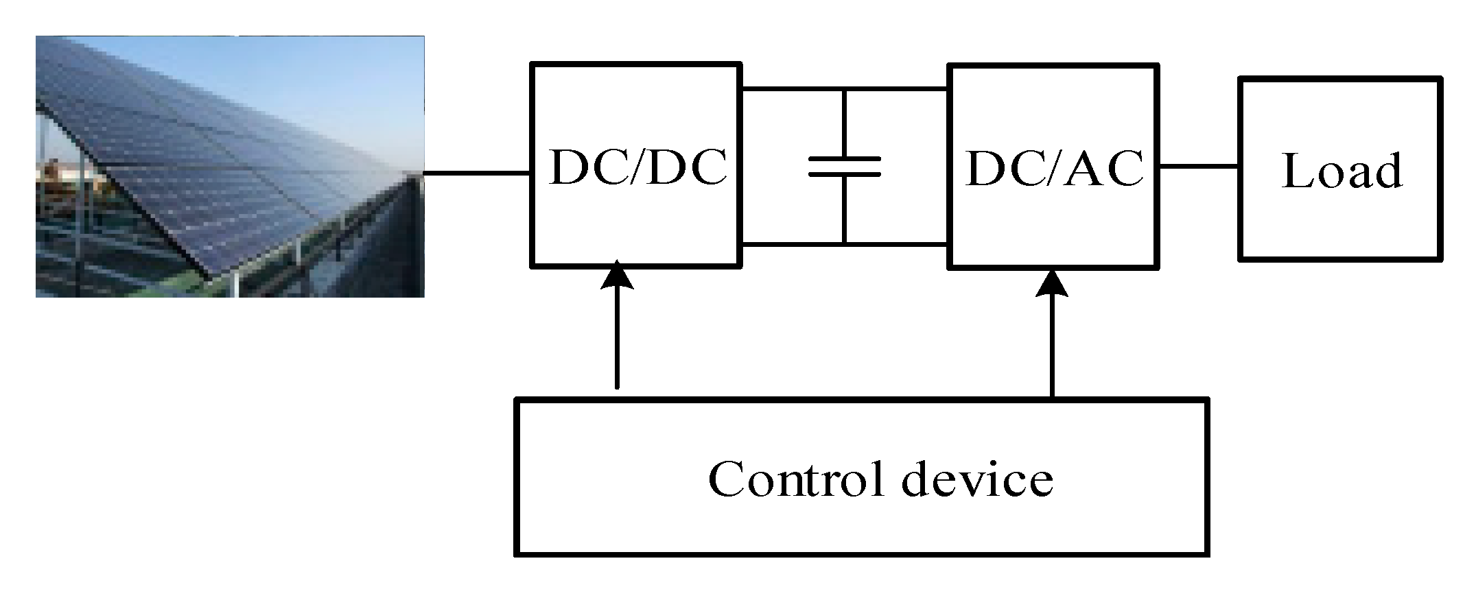
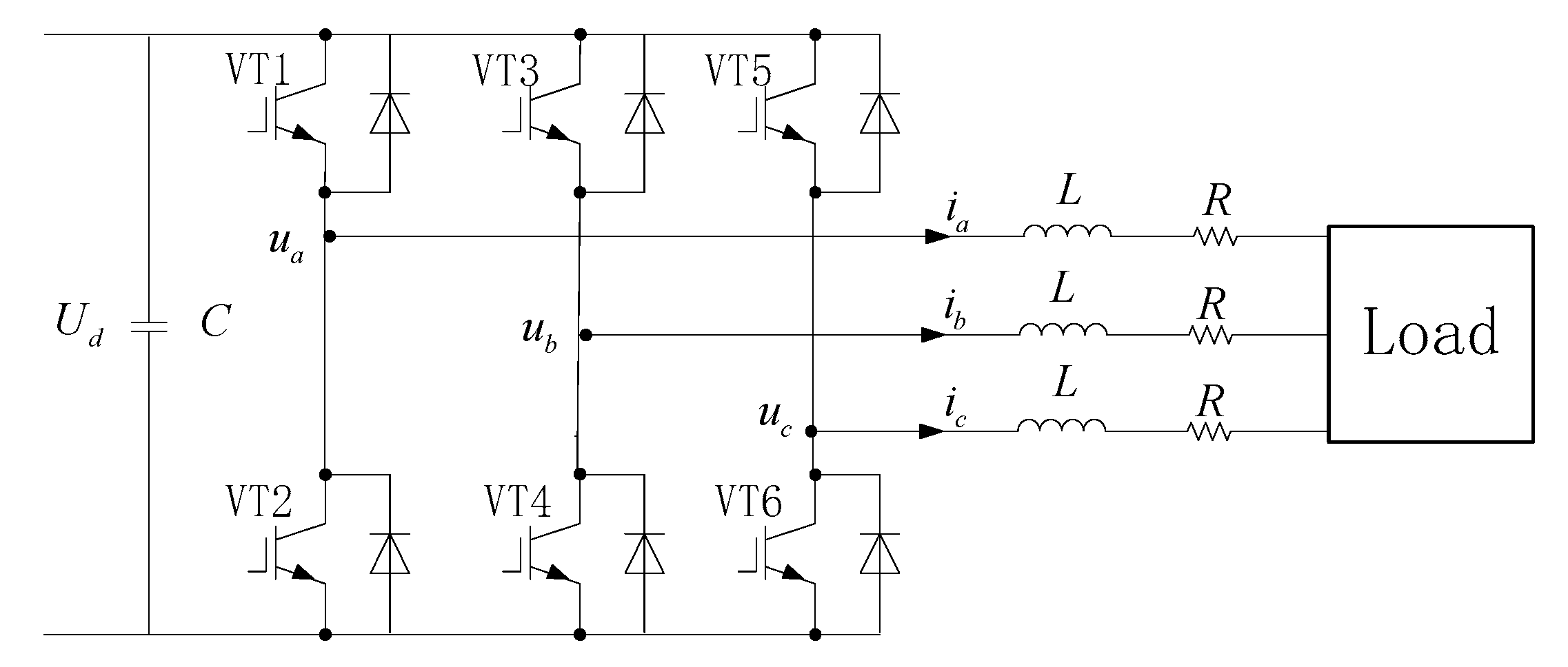
2. Equivalent Circuit of a PV Power System

Figure 1 shows the structure of a typical photovoltaic system. The MPPT control of PV panels is achieved by a DC/DC converter, which can also maintain the voltage stability of the DC bus. The PV inverter (DC/AC converter) can achieve the active/reactive power control.

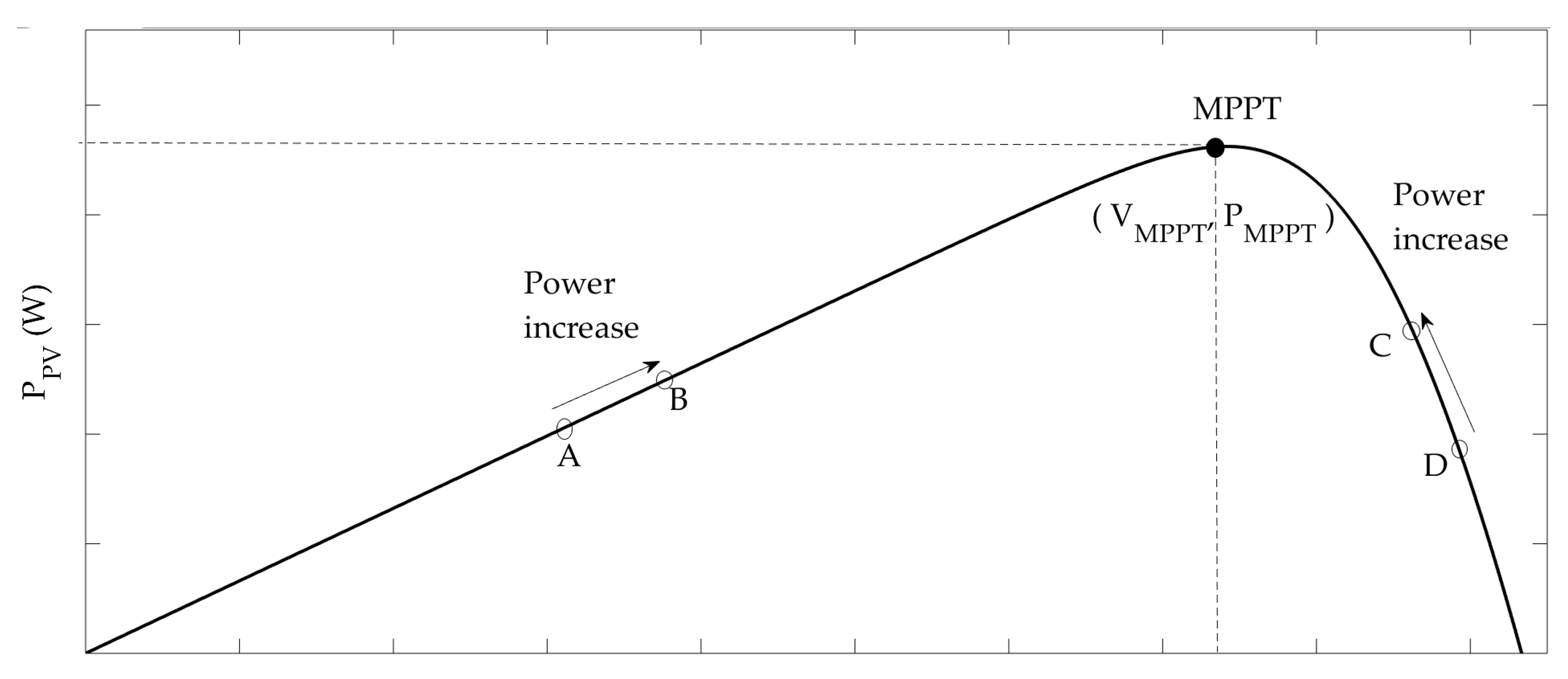
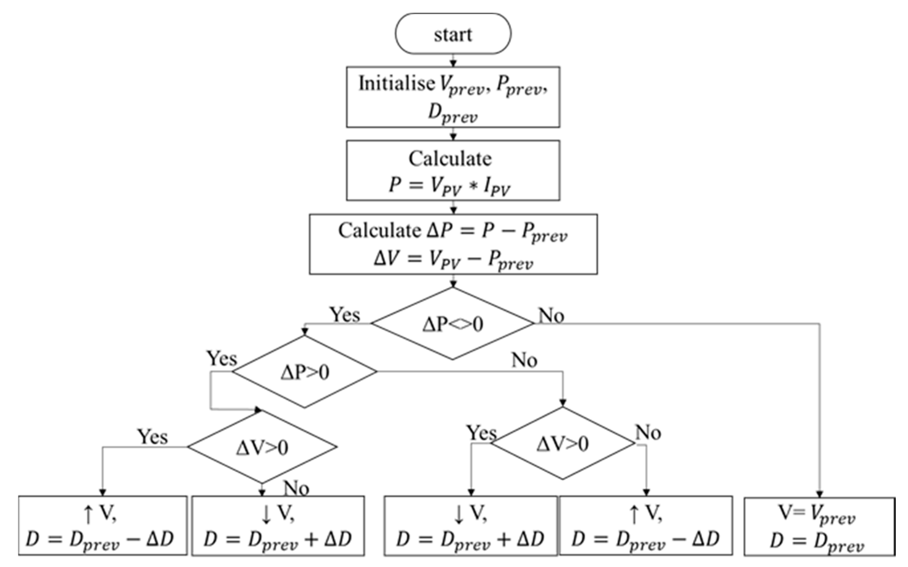
2.1. Perturbation and Observation (P&O) MPPT Algorithm

Conventionally, MPPT is embedded in a converter to determine the duty cycle that maximizes the PV power yield [22]. A perturbation and observation method (P&O) is used to find the maximum power point [23] by altering the array terminal voltage and then comparing the PV output power with its previous value. If the power increases while voltage increases, the PV array is operating in the correct direction; otherwise, the operational point should be adjusted to its the opposite direction [24,25]. The main advantage of P&O lies in its simplicity. This method shows its effectiveness, provided that solar irradiation does not change very quickly. As shown in Figure 2, there are four operational points, A, B, C and D. From point A to point B, the PV power increases while the voltage of point B is higher than that of point A. Therefore, the next perturbation voltage keeps increasing, or vice versa. If the operation starts from point C to D, PV power decreases while the voltage of point C is higher than the voltage of point D. The next operation should be changed to the opposite direction. Therefore, the next perturbation reduces the voltage so as to redirect the trajectory towards the maximum power point. Accordingly, four scenarios are summarized in Table 1.
A boost DC/DC converter is adopted to adjust the terminal voltage by regulating the duty ratio D. It will therefore incur the change of the equivalent power output which in turn realizes the maximum power output of a PV array. A flowchart of the P&O method is shown in Figure 3.

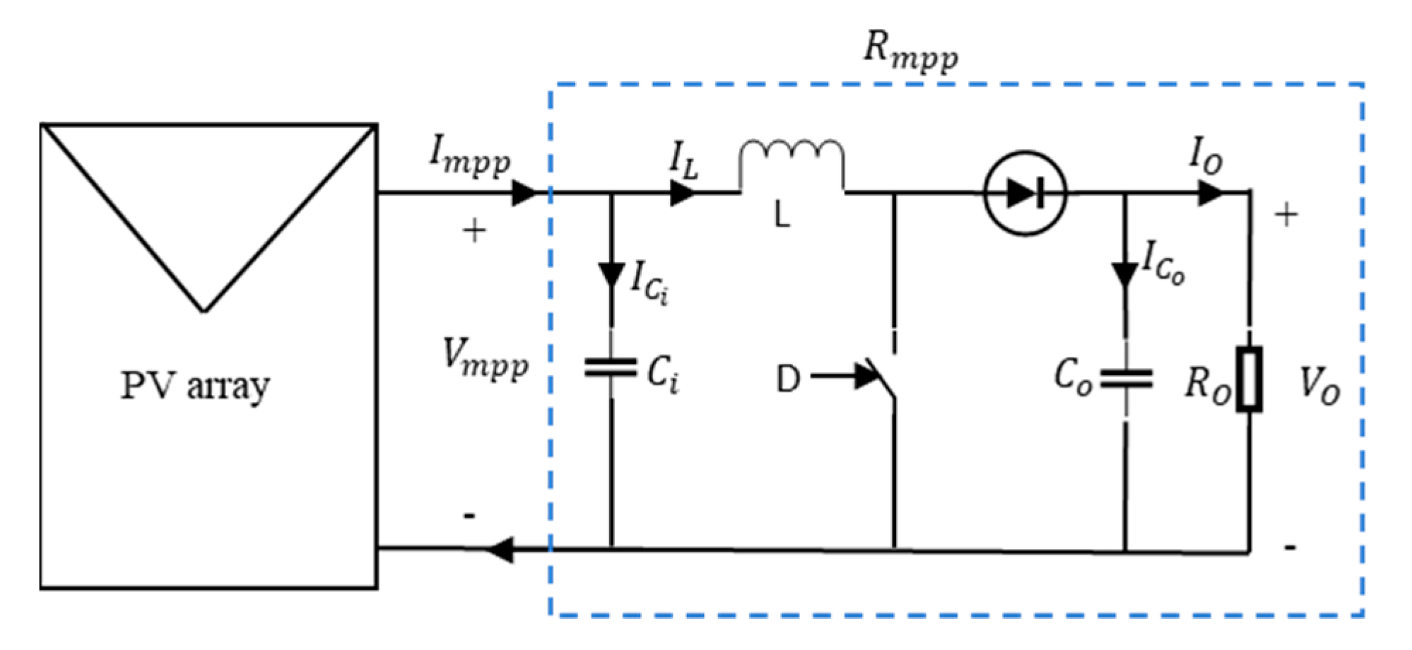
2.2. A Boost DC-DC Converter and the Equivalent Circuit

In this study, a boost converter is adopted to operate the voltage via changing D. A boost converter is expected to connect with the output of PV arrays to produce the equivalent output voltage equal to the voltage V m p p at the maximum power point, with equivalent resistance equal to R m p p with the current I m p p over the output circuit, as shown in Figure 4. Selecting a proper DC-DC converter with reasonable circuit parameters is essential.
To design a boost converter for a PV system, key elements in the selection include the inductance of an inductor L , the capacitance of an input capacitor C i , the input resistance R m p p , capacitance of an input capacitor C i , and the load resistance R O . The purpose of this boost converter is to realize the equivalent circuit resistance to R m p p . Therefore, the maximum output power under the current condition can be produced via this boost converter from a PV array.
The maximum power point resistance R m p p is calculated based on the maximum power point voltage V m p p and the maximum power point current I m p p by using a simple calculation in Equation (1).   R O can be calculated by Equation (2). The duty ratio D can be derived from Equation (3). Assuming there is no power loss in circuit, an energy balance equation can be established (Equation (4)).
R m p p = V m p p I m p p
R O = R m p p ( 1 D ) 2
Or     D = 1 R m p p R O
p m p p = V m p p 2 R m p p = V O 2 R O
Or    V m p p 2 V O 2 = R m p p R O
Equation (5) presents the relationship between resistance and voltage. The output voltage is calculated from Equation (5) to Equation (6).
V O = V m p p R O R m p p
The inductance can be estimated by many methods [26,27]. A general calculation is given by Equation (7).
L = V m p p · D I m p p · γ I L · f
where f and γ I L refer to the switching frequency and the inductor current ripple factor.
Input capacitor C i can be calculated according to Equation (8).
C i = D 8 · L · γ V m p p · f 2
Output capacitor C O can be calculated according to Equation (9) [28].
C O = D R O · γ V O · f
where the current ripple factor γ I L and the voltage ripple factors γ V m p p , γ V O are refined within 5%.

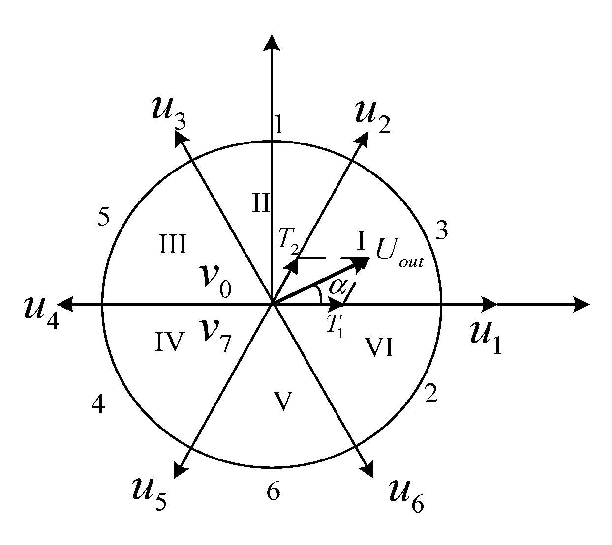
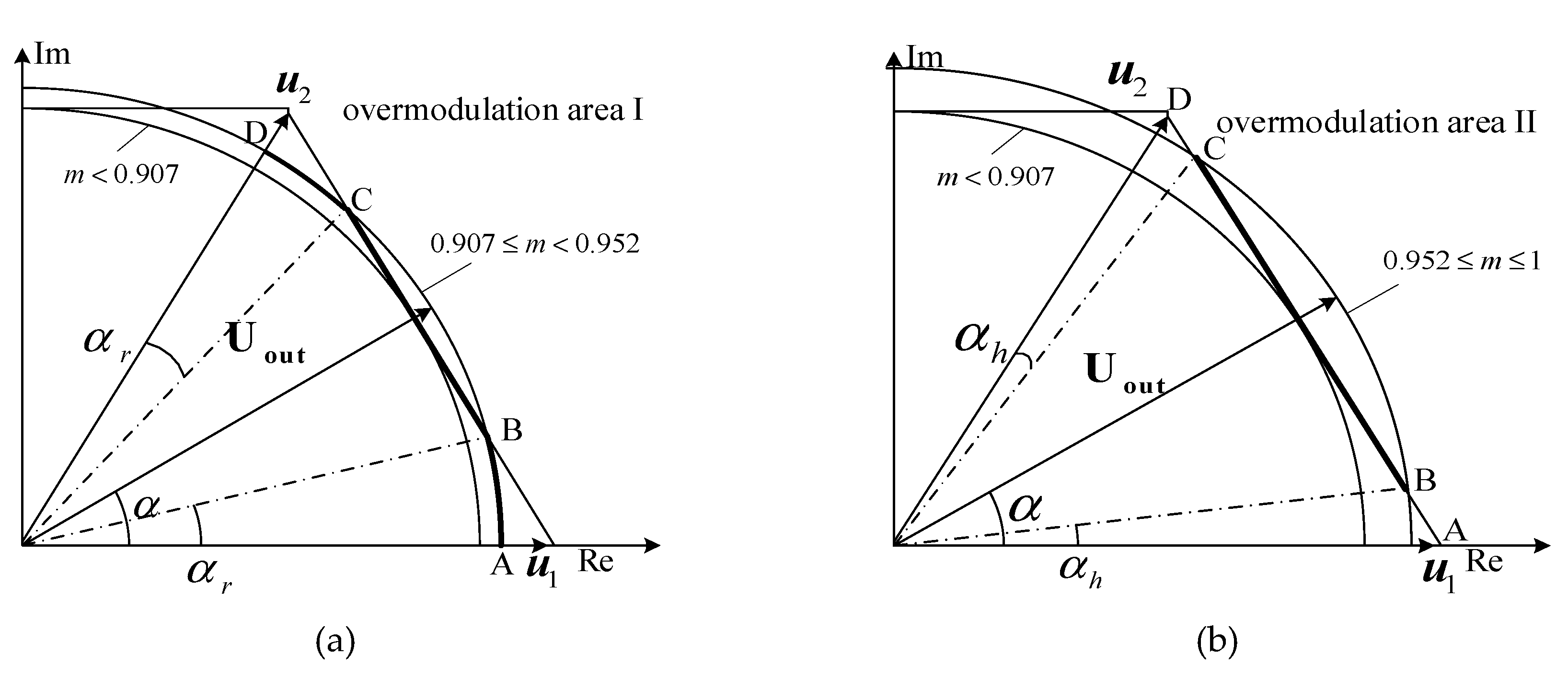
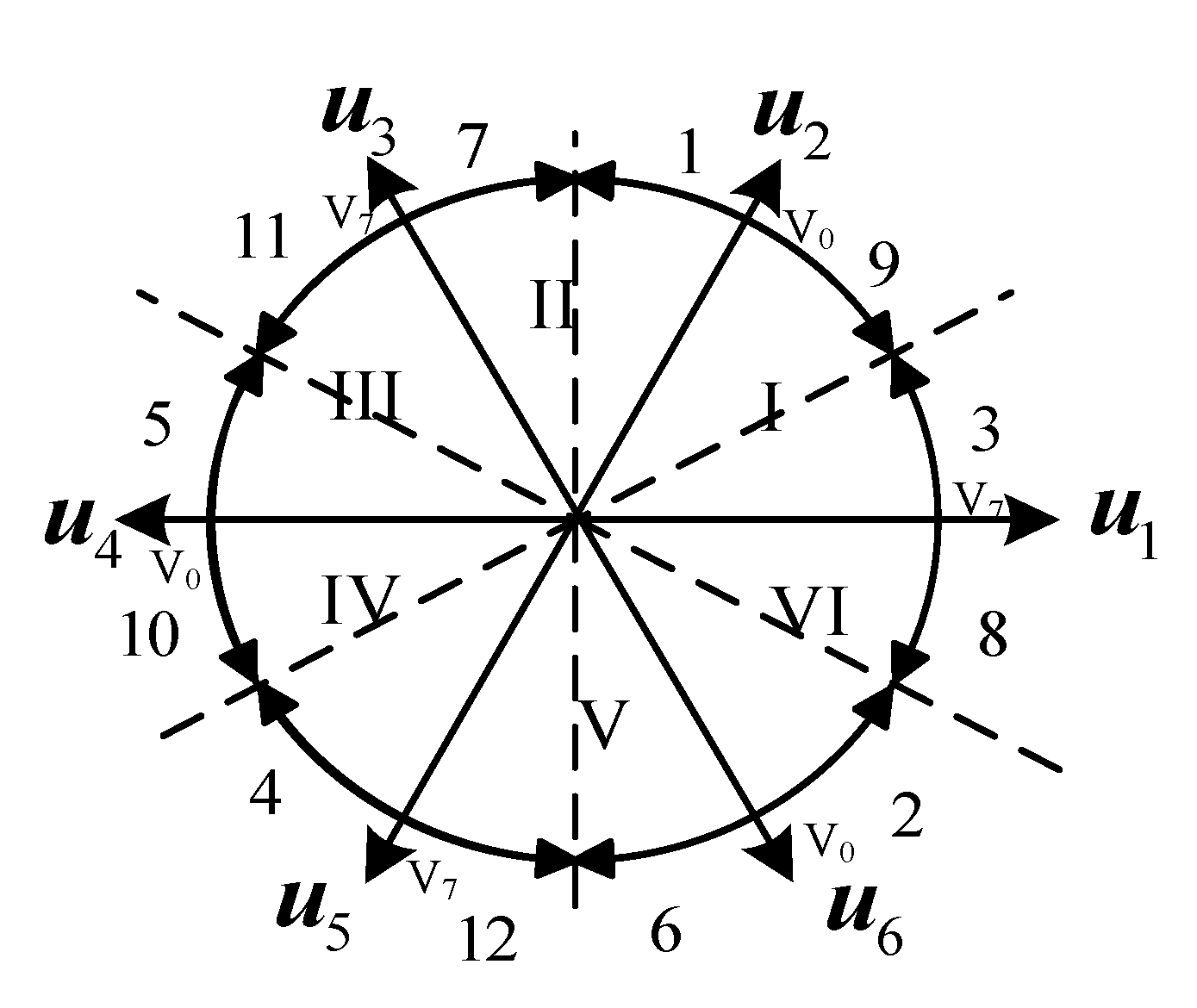
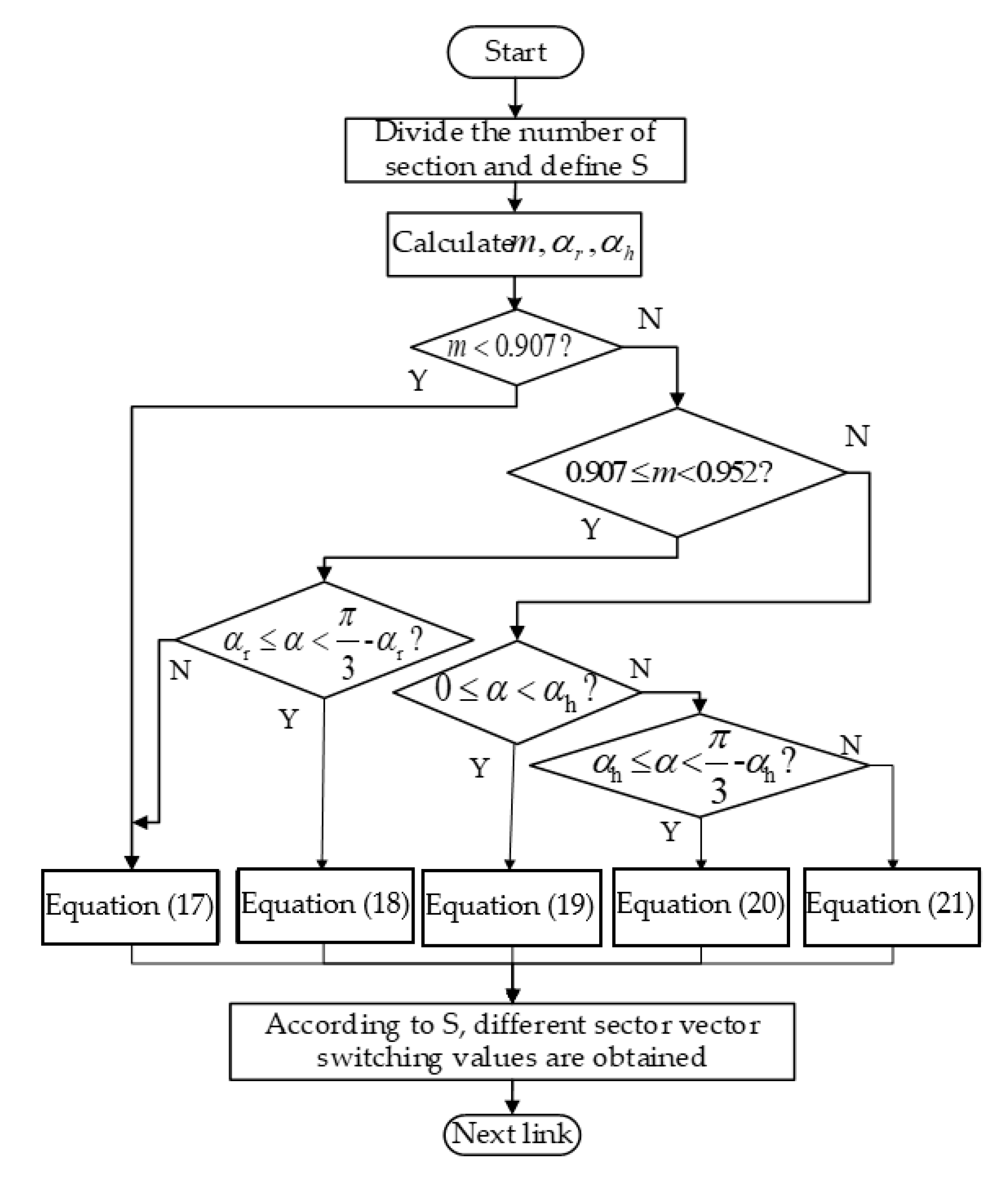
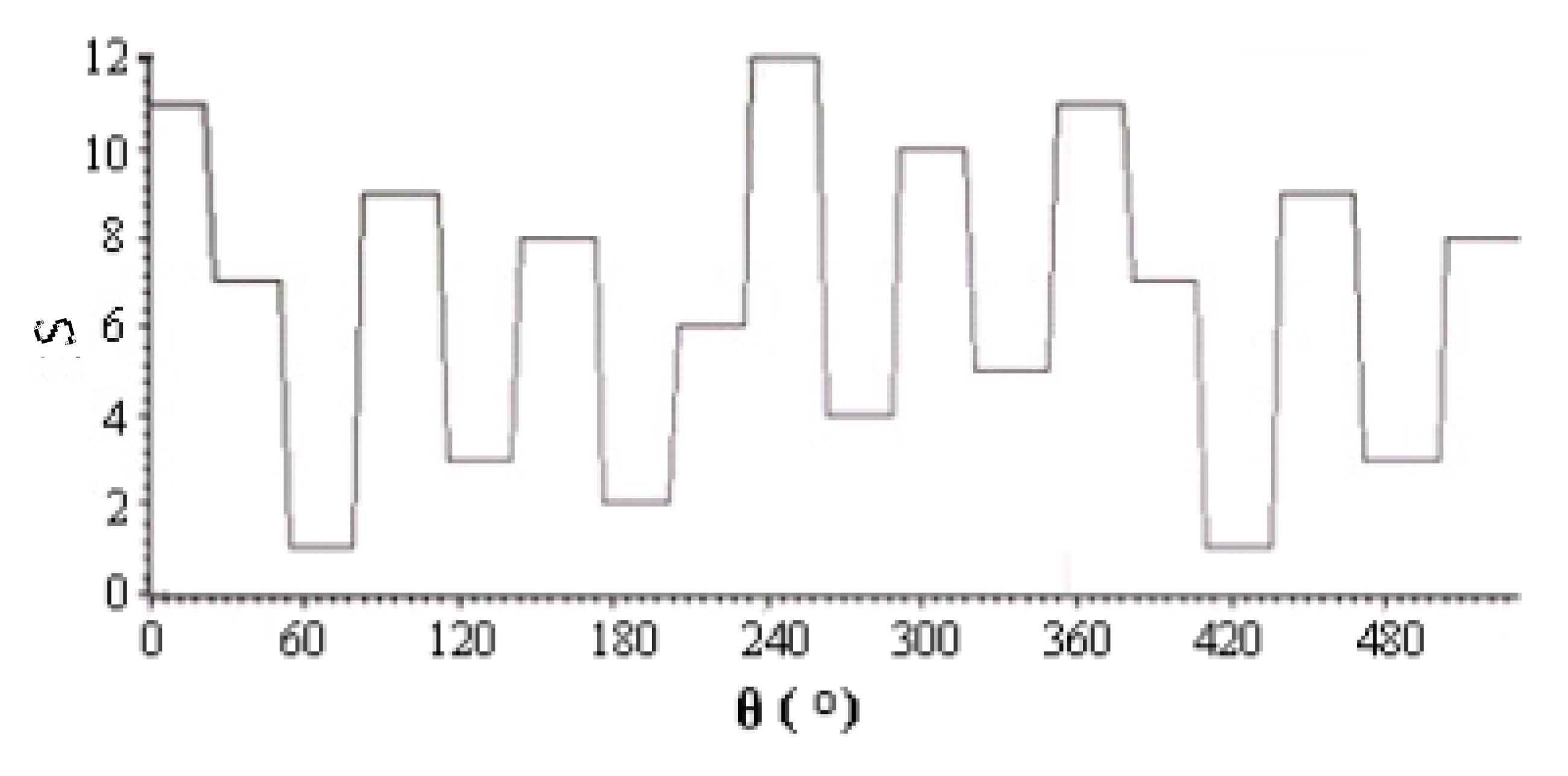
2.3. Division of the Overmodulation Area

Figure 5 presents the main circuit topology of the three-phase grid-tie inverter, where U d is the DC-link voltage, i a , i b , and i c are the inverter output currents, L is the filter inductance, and R is the filter inductance equivalent series resistance, respectively.
In the inverter, the on-state of the upper arm switches and the off-state of the lower arm switches are defined as “1”; otherwise, they are “0”. Therefore, the three bridge arms of the inverter have eight switch states, corresponding to eight basic voltage space vectors: u 0 (000), u 1 (100), u 2 (110), u 3 (010), u 4 (011), u 5 (001), u 6 (101) and u 7 (111). The SVPWM modulation voltage vector and the sector distribution of the PV inverter are demonstrated in Figure 6. The amplitude of u 1 ~ u 6 is 2 3 U d , and the phase angles of u 1 ~ u 6 differ by 60°.
According to the volt-second balance principle:
U o u t · T s = u 1 · T 1 + u 2 · T 2
where U o u t is the given output voltage vector, T 1 is the action time for u 1 , T 2 is the action time for u 2 , and T s is the switching period.
The output space rotating vector with a constant rotating speed and a constant amplitude is achieved by the vector addition of adjacent vectors. The output range is in the inscribed circle of the regular hexagon constituted by the vectors u 1 ~ u 6 , which are also known as the linear modulation areas. The maximum amplitude of the output phase voltage is given by:
u m _ l i n e = 2 · U d 3 · cos 30 ° = U d 3
If the PV inverter is controlled by the six-step wave mode outside of the linear modulation area, the amplitude of the phase voltage can be obtained [29].
u m _ m a x = 2 · U d π
The region from outside the linear modulation area to the six-step maximum output voltage area is called the overmodulation area. The modulation coefficient m is defined as:
m = π · U o u t 2 · U d
There are three different regions as per the modulation coefficient. In the linear modulation area, m < 0.907 ; in the overmodulation area I, 0.907 < m < 0.952 ; in the overmodulation area II, 0.952 < m < 1 . Figure 7 shows the trajectory of the synthesized voltage vector in the overmodulation areas. The simplified formulas for overmodulation areas I and II are given by [30,31,32,33].
α r = π 6 arccos ( U d 3 · U o u t )
{ α h = 6.40 · m 6.09 ( 0.952 m < 0.9800 ) α h = 11.57 · m 11.34 ( 0.9800 m < 0.9975 ) α h = 48.96 · m 48.43 ( 0.9975 m < 1 )
Take sector I for example. In overmodulation area I, the rotational speed of the output voltage vector remains constant and the amplitude is limited by the hexagon. The vertex of the trajectory follows the thick solid line of ABCD. In overmodulation area II, the rotation speed of the output voltage vector changes and the amplitude is limited. When α < α h , the output voltage vector is u 1 . When α h α < π 3 α h , the trajectory of the output voltage vector is the BC solid line. When α π 3 α h , the output voltage vector is u 2 . When α h = π 6 , the output voltage vector traces at the vertex of the regular hexagon, and the modulation coefficient is the maximum (m = 1). The remaining sectors are the same.

2.4. Full Modulation Region Voltage Vector

The key to controlling the voltage vector in the full modulation area is to determine the action time of the voltage vector according to the modulation coefficient m.
Take sector I for example again: U o u t is synthesized by two basic voltage space vectors u 1 (100) and u 2 (110) and it is known that u 1 = 2 3 U d , u 2 = 2 3 U d · e j π 3 . According to the sine theorem:
U o u t sin 2 π 3 = u 1 ·   T 1 T s sin ( π 3 α ) = u 2 ·   T 2   T s sin ( α )
The action time T 1 and T 2 can be further calculated. When T 1 + T 2 < T s , the zero vector u 0 (000) or u 7 (111) is used to fill the remaining time T 0 .
(1) SVPWM linear modulation area ( m < 0.907 )
It can be obtained from Equation (16):
{ T 1 = 3 · T s ·   U o u t U d · sin ( π 3 α ) T 2 = 3 · T s ·   U o u t U d · sin ( α ) T 0 = T s T 1 T 2
(2) Overmodulation area I ( 0.907 m < 0.952 )
(i) When 0 α α γ or π 3 α γ α π 3 , T 1 , T 2 and T 0 are calculated in the same way as Equation (17).
(ii) When α γ α < π 3 α γ ,
{ T 1 = T s ·   sin ( π 3 α ) sin ( π 3 + α ) T 2 = T s ·   sin ( α ) sin ( π 3 + α ) T 0 = 0
(3) Overmodulation area II ( 0.952 m < 1 )
(i) When 0 α < α h ,
T 1 = T s ,   T 2 = 0 ,   T 0 = 0
(ii) When α h α < π 3 α h ,
  γ = π 6 · ( α α h ) (   π 6 α h )
{ T 1 = T s ·   sin ( π 3 γ ) sin ( π 3 + γ ) T 2 = T s ·   sin γ sin ( π 3 + γ ) T 0 = 0
(iii) When π 3 α h α < π 3 ,
T 1 = 0 ,   T 2 = T s ,   T 0 = 0

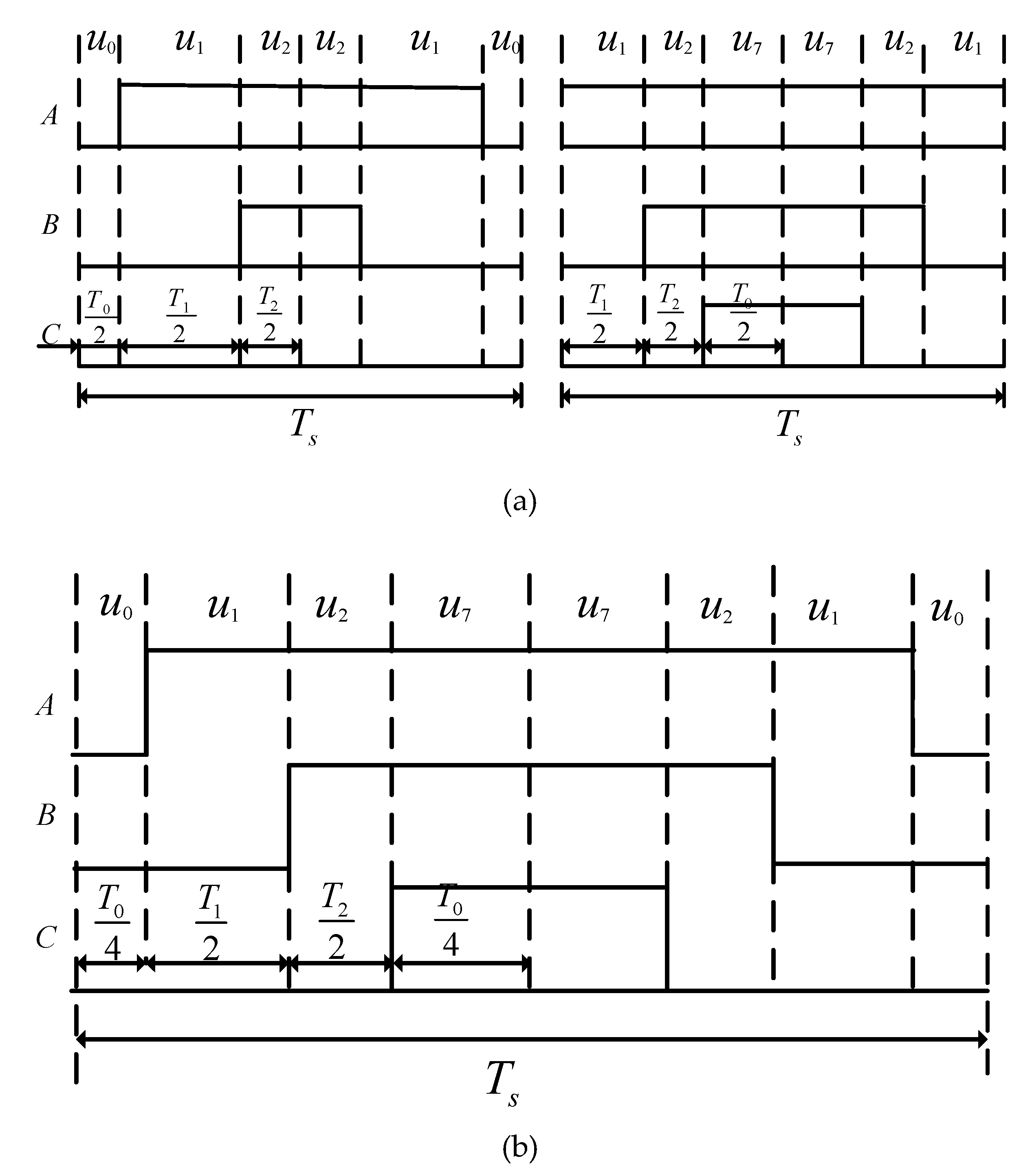
3. DPWM Overmodulation Algorithm

In traditional SVPWM modulation algorithms, A, B, and C from the given voltage vector U o u t are calculated from the α β coordinate plane.
{ A = U β B = U α ·   sin 60 ° U β · cos 60 °   C = U α ·   sin 60 ° U β · cos 60 °
where U α and U β are the α ,   β components of U o u t in the α β coordinate plane, respectively. S is defined as:
S = sign ( A ) + 2 · sign ( B ) + 4 · sign ( C )
Thus, the relationship between sectors N and S can be obtained, as shown in Table 2.
As for the DPWM scheme, the switches are controlled only by the zero vector u 0 or u 7 in a triangular carrier cycle, as shown in Figure 8. u 7 is selected in the 60° range centred around the basic vectors u 1 , u 3 and u 5 , while u 0 is selected in other sectors. The DPWM sector number and its action conditions are tabulated in Table 3. There are twelve 30° sectors in the DPWM, as compared to six sectors in conventional SVPWM.
As for the DPWM modulation, the power devices switch four times in one sector because only u 0 or u 7 is used as the zero vector in one sector. Meanwhile, for the SVPWM modulation, the power devices switch six times in one sector because the vectors u 0 and u 7 are simultaneously applied (each action time is T 0 / 2 ).
Therefore, the switching frequency of the power devices in the DPWM modulation is reduced by one-third compared to the SVPWM modulation, and the switching sequence of the first sector is shown in Figure 9. According to the literature [34], the switching losses of the inverter power device include turn-on loss P o n and turn-off loss P o f f :
P o n = 1 8 · U d · t r N · I C M 2 I C N · f s
P o f f = U d · I C M · t f N · f s · ( 1 3 π + 1 24 · I C M I C N )
where t r N and t f N are the turn-on time and turn-off time, respectively; f s is the switching frequency of power devices; I C N is the forward current of IGBT; I C M is the amplitude of the sinusoidal current.
Switching losses are proportional to f s according to Equations (26) and (27), so the switching losses of the DPWM modulation can be reduced by one-third compared to the switching losses of the SVPWM modulation.

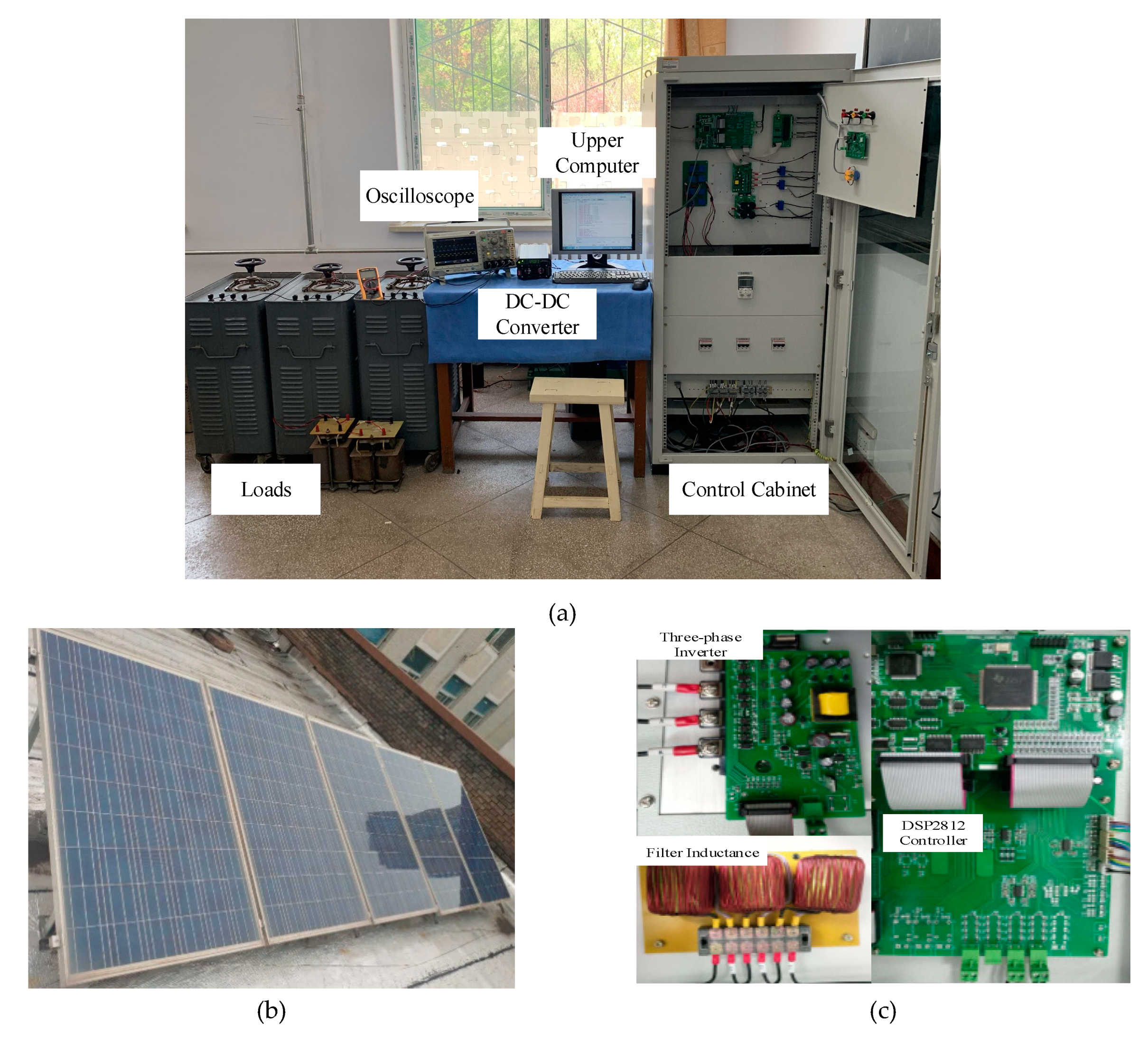
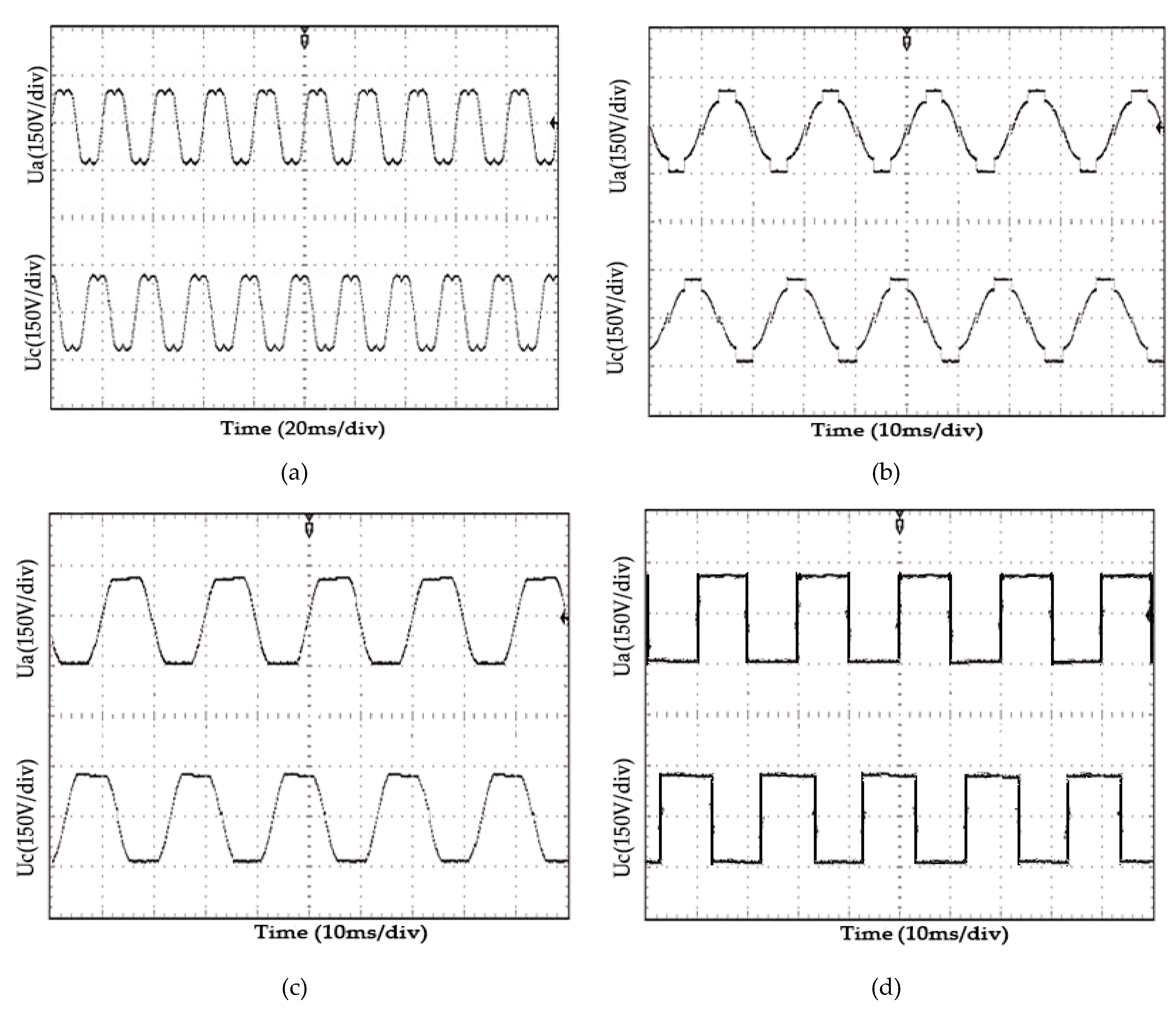
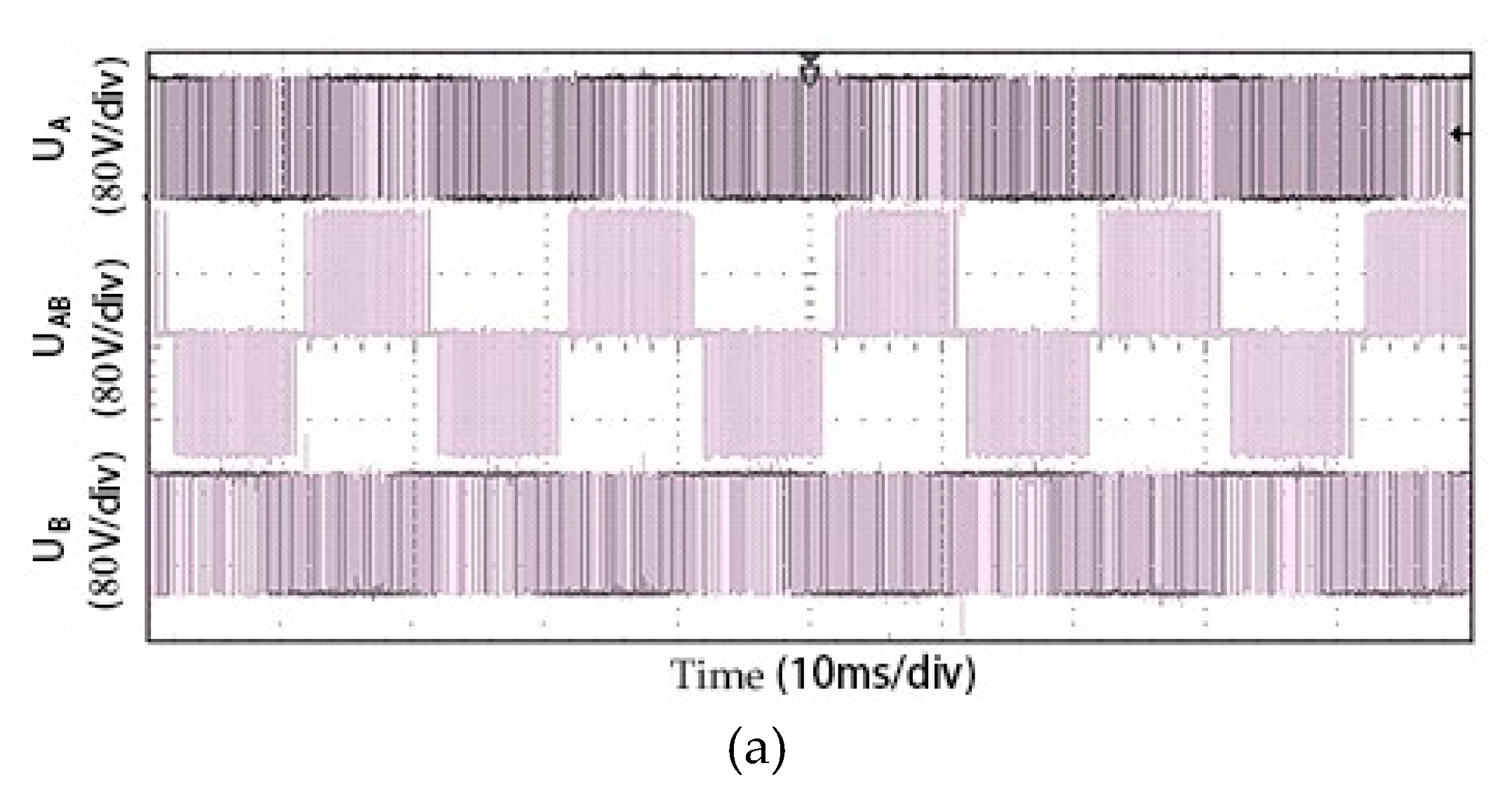
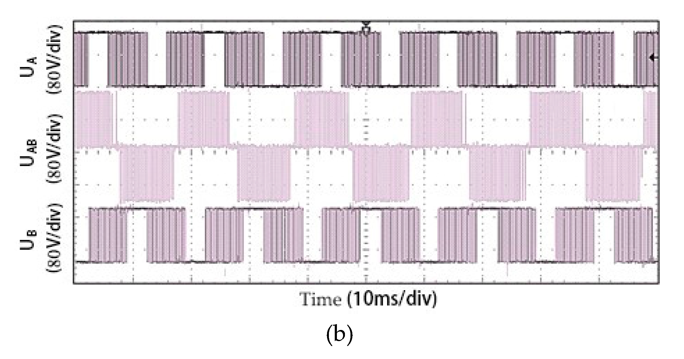
4. Simulation and Experimental Validation of the Proposed Scheme

A PV inverter experimental test rig based on digital signal processing (DSP) is developed to verify the DPWM control algorithm as Figure 10a shown. DSP takes a high-performance 32-bit fixed-point TMS320F2812 as the controller (clock frequency 150 MHz, working voltage 3.3 V, Texas Instruments Incorporated, TX, USA); its chip contains 128 K 16-bit FLASH, 16-way 12-bit A/D conversion, two event managers and so on. Experimental tests are carried out by five photovoltaic panels (as shown in Figure 10b) in series under an ambient temperature of 25 °C and a daylight illuminance of 1000 W/m2; the parameters of a single photovoltaic module are presented in Table 4. The output voltage range of the DC/DC converter (5 kW) is 100‒400 V. The power module model of the DC/AC converter (2 kW) is PM30RSF060 (as shown in Figure 10c), and its maximum switching frequency is 20 kHz.
Before the proposed system is validated by the experimental tests, an MPPT algorithm with the associated equivalent circuit is simulated.

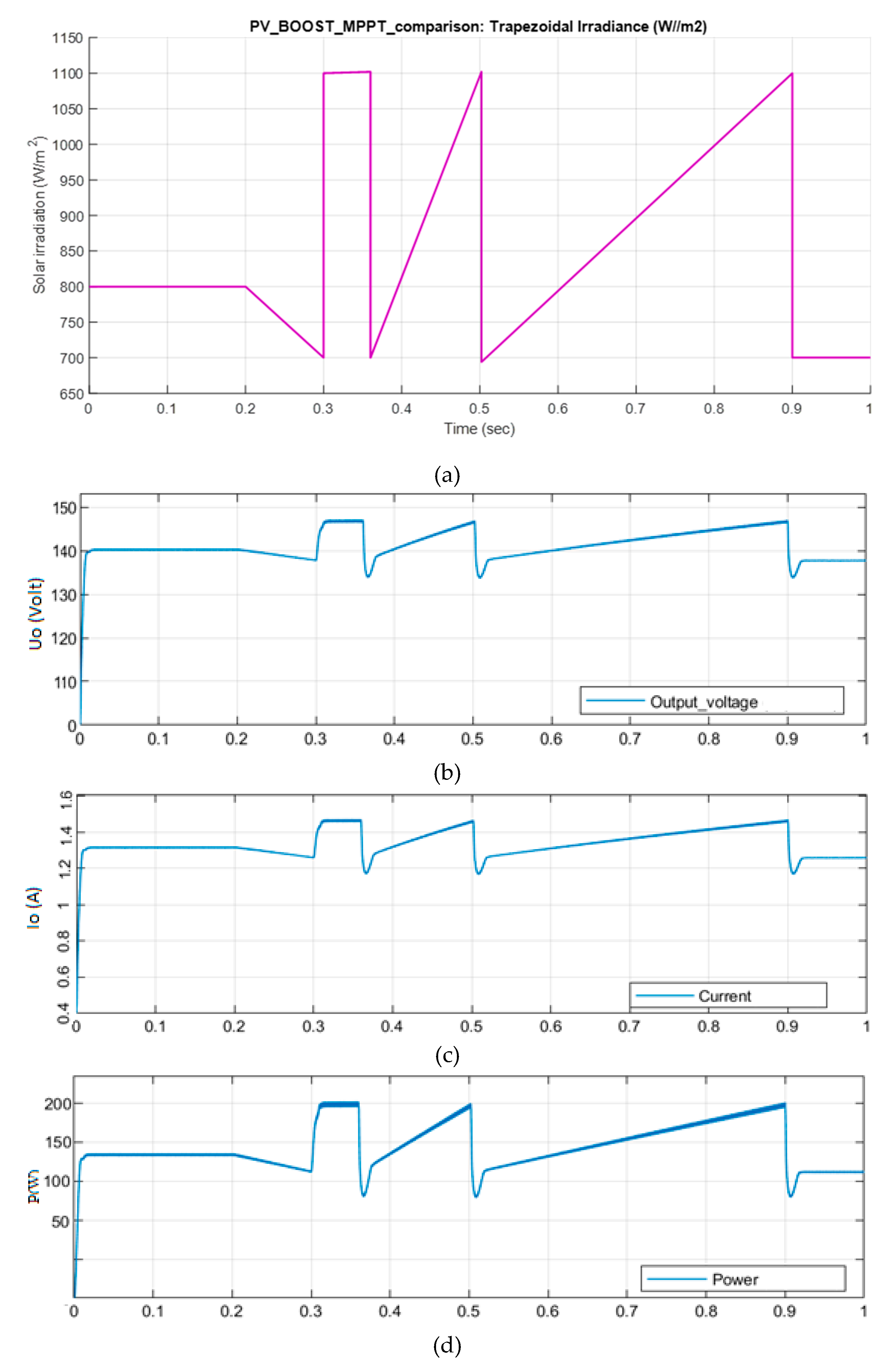
4.1. Simulation Results of Different Varied Solar Irradiations

In a PV power system, the weather conditions, such as cloudy, rainy, dust, etc., will influence the power conversion. In most applications in this field, solar irradiation is considered as one of the most important factors in power generation, where weather variation will be mostly reflected in solar irradiation. We therefore test the PV power system performance as the solar irradiation varies. A series of waveforms in Figure 11 provides the auto-tracking process when the MPPT algorithm works with the DC/DC converter. Through the DC/DC converter, the output DC voltage of photovoltaic modules is kept at 140 V while the duty ratio D is 0.735 in the reference condition. In order to validate the performance of a DC/DC converter with the MPPT algorithm, varied solar irradiations are applied to the PV array. The performance is shown in Figure 11a–d.
As Figure 11a–d show, the current, the voltage and the power of the PV panel spontaneously follow the rapid variation of the solar irradiation. The proposed PV power system reaches the target of maximal utilisation of solar energy with limited oscillation, which in turn validates the excellent performance of the MPPT scheme applied in this investigation.

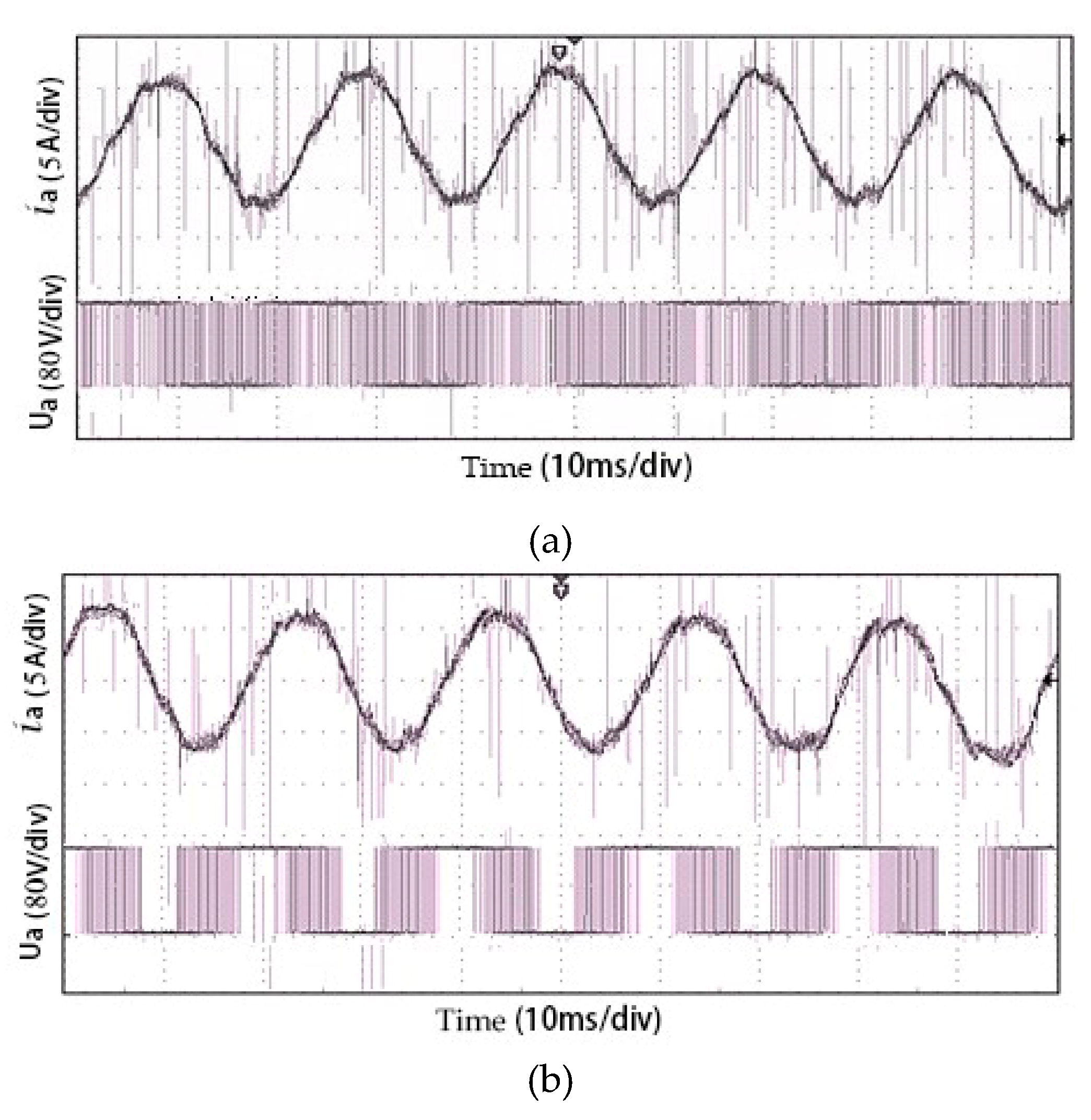
4.2. DC/AC under the DPWM scheme

The DC/AC converter runs with a three-phase symmetrical resistive load ( R L = 40 Ω, L L = 10 mH). The switching period is selected as T s = 0.0002 s. The test waveforms are collected by the Tektronix oscilloscope TDS2024 (Test equipment Solutions Ltd, Berkshire, UK).
The control algorithm is designed to implement the proposed DPWM scheme. The flow chart of the DPWM algorithm can be obtained according to Equations (17)‒(21), as shown in Figure 12.
The transformation sequence of the DPWM overmodulation sector is shown in Figure 13.
The SVPWM modulation waveform in the linear modulation area and the DPWM modulation waveform with different modulation coefficients are shown in Figure 14.
It can be seen from the figures that as the modulation coefficient increases, the peak of the DPWM modulation wave is gradually flattened and finally operates in the square wave operation state, thereby achieving linear control of the inverter output fundamental voltage over the entire modulation range.
When the modulation coefficient m = 0.92, the output pulse waveforms of TMS320F2812 under different strategies are shown in Figure 15. The waveforms of the output phase voltage and current are presented in Figure 16 and the spectral analysis results of the current are shown in Figure 17.
From Figure 15, Figure 16 and Figure 17, it can be seen that the upper and lower arms are not operated in the one-third period under the proposed strategy. Compared with the switching control pulse of conventional SVPWM with the same carrier frequency, the switching time is reduced by one-third. The switching losses can be effectively reduced so as to increase the efficiency. The harmonic contents of the load current measured by the spectrum analyzer are presented in Figure 17 and Table 5.
Clearly, the amplitude of the 5th, 7th and 11th harmonics under the DPWM modulation strategy are lower than that of the SVPWM modulation strategy. The THD of the conventional SVPWM modulation strategy is 6.58%, while that of the DPWM overmodulation strategy is reduced to 4.4%. The current waveforms of the proposed DPWM algorithm are close to sinusoidal, and it appears to have a higher utilization ratio of the DC voltage than the SVPWM. In turn, this leads to reduced switching losses and improved THD.

5. Conclusions

This paper has proposed a high-efficiency PV power generation system by combining an MPPT algorithm and a new control technology evolving from DPWM and overmodulation. It can realize the modulation of a full area on the basis of traditional SVPWMs. A DC/DC converter with an inverter simulation model and an experimental test rig are developed to justify the proposed method. The main contributions of this work are:
(i)
A P&O MPPT algorithm is applied to a boost DC/DC converter so as to effectively harvest solar energy and transform to DC electricity;
(ii)
A novel control technology is proposed, combining discontinuous pulse width modulation (DPWM) and overmodulation technology to better utilize the DC-link voltage.
(iii)
It has been shown by measurements that through implementing this algorithm, the switching losses in the power electronic devices are reduced.
(iv)
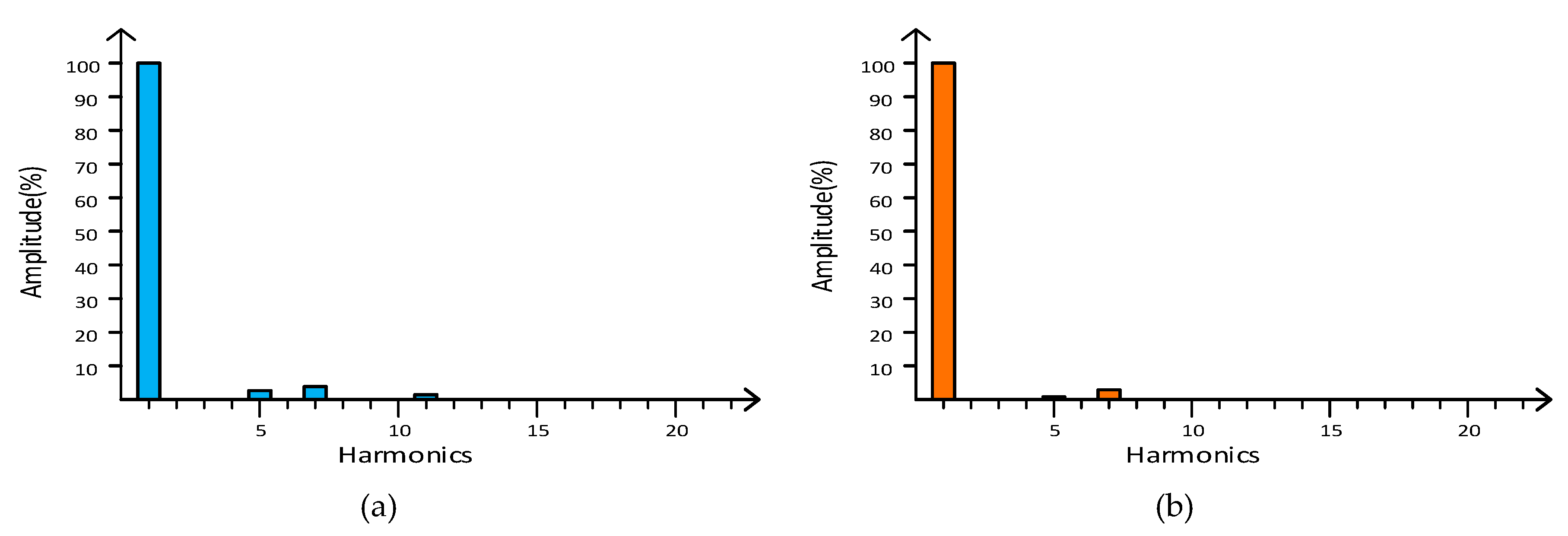
The test results have confirmed that the DPWM overmodulation algorithm can effectively reduce harmonic distortion of the three-phase output voltage and current. It has also improved the conversion efficiency of photovoltaic systems.
(v)
The proposed technology is simple to implement in practical PV inverters as there are no alterations to existing hardware design. It may also be applied to other grid-tie inverters to improve their performance.

Author Contributions

In this article, L.L. and W.C. conceived and designed the system; H.W., L.C. and B.L. performed the experiments; A.A.S.B. and X.C. built the simulation models; X.C. and L.L. analyzed data and wrote the paper.

Funding

This study is funded by the Royal Society of the UK, National Natural Science Foundation of China (NSFC 51867007, 51867005) and the Shanxi Province Natural Science Foundation of China.

Conflicts of Interest

The authors declare no conflict of interest.

Nomenclature

α Angle between the output voltage vector and the horizontal axis
α γ Angle between the intersection of the output voltage vector and the hexagon boundary, and the vertex of hexagon
α h Control angle to determine how long the output voltage vector stays at the vertex of hexagon
γ I L Current ripple factor of the inductor
γ V O Voltage ripple factor of the inductor
C i ,Capacitance of the input capacitor in DC/DC converter
C o ,Capacitance of the output capacitor in DC/DC converter
D Duty ratio of DC/DC converter
f Switching frequency of a DC/DC converter
i a , i b , i c Inverter output currents
I m p p Equivalent output current at maximum power point
LFilter inductance
L L Symmetrical load inductance
L Inductance of a DC/DC converter
mModulation coefficient
NSector
p m p p Maximum power of a PV module
RFilter inductance
RLSymmetrical load resistance
R m p p Equivalent resistance at maximum power point
R O Load resistance of the DC/DC converter
SSector number
T 1 , T 2 ,   T 0 Action time of adjacent fundamental voltage vectors and zero vector
T s Switching period
u 0 ~ u 7 Basic voltage space vectors
U α , U β Two components of the output voltage vector in the α β coordinates
U d DC-link voltage
u m Amplitude of the phase voltage
u m _ m a x Maximum phase voltage in linear modulation area
U o u t Output voltage
V m p p Equivalent output voltage at maximum power point
V O Load voltage of the DC/DC converter
t r N Turn-on time
t f N Turn-off time
f s Switching frequency of power devices
I C N Forward current of IGBT
I C M Amplitude of the sinusoidal current

References

  1. Bukhari, S.A.A.S.; Cao, W.P.; Soomro, T.A.; Guanhao, D. Future of microgrids with distributed generation and electric vehicles. In Development and Integration of Microgrids; Cao, W.P., Yang, J., Eds.; InTech: Rijeka, Croatia, 2017. [Google Scholar]
  2. Aly, M.; Ahmed, E.M.; Shoyama, M. Modulation Method for Improving Reliability of Multilevel T-type Inverter in PV Systems. IEEE J. Emerg. Sel. Top. Power Electron. 2019. [Google Scholar] [CrossRef]
  3. Gosumbonggot, J.; Fujita, G. Global Maximum Power Point Tracking under Shading Condition and Hotspot Detection Algorithms for Photovoltaic Systems. Energies 2019, 12, 225. [Google Scholar] [CrossRef]
  4. Baimel, D.; Tapuchi, S.; Levron, Y.; Belikov, J. Improved Fractional Open Circuit Voltage MPPT Methods for PV Systems. Electronics 2019, 8, 321. [Google Scholar] [CrossRef]
  5. Afzal Awan, M.M.; Mahmood, T. A Novel Ten Check Maximum Power Point Tracking Algorithm for a Standalone Solar Photovoltaic System. Electronics 2018, 7, 327. [Google Scholar] [CrossRef]
  6. Boobalan, S.; Dhanasekaran, R. Hybrid topology of asymmetric cascaded multilevel inverter with renewable energy sources. In Proceedings of the 2014 International Conference on Advanced Communication Control and Computing Technologies (ICACCCT), Ramanathapuram, India, 8–10 May 2014; pp. 1046–1051. [Google Scholar]
  7. Ali, W.H.; Cofie, P.; Fuller, J.H.; Lokesh, S.; Kolawole, E.S. Performance and efficiency simulation study of a smart-grid connected photovoltaic system. Energy Power Eng. 2017, 9, 71. [Google Scholar] [CrossRef]
  8. Djokic, S.; Langella, R.; Meyer, J.; Stiegler, R.; Testa, A.; Xu, X. On evaluation of power electronic devices efficiency for nonsinusoidal voltage supply and different operating power. IEEE Trans. Instrum. Meas. 2017, 66, 2216–2224. [Google Scholar] [CrossRef]
  9. Zhang, X.; Li, J.; Zhao, W.; Tao, L. Review of high efficiency photovoltaic inverter. Chin. J. Power Sources 2016, 4, 931–934. [Google Scholar]
  10. Wilkinson, S.; Gilligan, C. PV Inverter Service Plans & Extended Warranties Report—2013; HIS Technology: London, UK, 2013. [Google Scholar]
  11. Suresh, K.; Prasad, M.V. Performance and evaluation of new multilevel inverter topology. Int. J. Adv. Eng. Technol. 2012, 2, 485–494. [Google Scholar]
  12. Zhu, X. Three level and efficiency of photovoltaic Inverter. Electr. Age 2016, 8, 46–47. [Google Scholar]
  13. Griva, G.; Oleschuk, V. Synchronous operation of dual-inverter-based photovoltaic system with low DC-voltages. In Proceedings of the 2010 International Conference on Electrical Machines (ICEM), Rome, Italy, 6–8 September 2010; pp. 1–6. [Google Scholar]
  14. Park, Y.; Sul, S.K.; Hong, K.N. Overmodulation strategy for current control in photovoltaic inverter. IEEE Trans. Ind. Appl. 2016, 1, 322–331. [Google Scholar] [CrossRef]
  15. Chen, W.; Sun, H.; Gu, X.; Xia, C. Synchronized space-vector PWM for three-level VSI with lower harmonic distortion and switching frequency. IEEE Trans. Power Electron. 2016, 31, 6428–6441. [Google Scholar] [CrossRef]
  16. Beig, A.; Kanukollu, S.; Hosani, K.; Dekka, A. Space-vector-based synchronized three-level discontinuous PWM for medium-voltage high-power VSI. IEEE Trans. Ind. Electron. 2014, 61, 3891–3901. [Google Scholar] [CrossRef]
  17. Mathew, J.; Mathew, K.; Azeez, N.B.; Rajeevan, P.P.; Gopakumar, K. A hybrid multilevel inverter system based on dodecagonal space vectors for medium voltage IM drives. IEEE Trans. Power Electron. 2013, 28, 3723–3732. [Google Scholar] [CrossRef]
  18. Carrasco, G.; Silva, C.A. Space vector PWM method for five-phase two-level VSI with minimum harmonic injection in the overmodulation region. IEEE Trans. Ind. Electron. 2013, 5, 2042–2053. [Google Scholar] [CrossRef]
  19. Holmes, D.; Lipo, T. Pulse Width Modulation for Power Converters: Principles and Practice; Wiley IEEE Press: Piscataway, NJ, USA, 2003. [Google Scholar]
  20. Elmelegi, A.; Aly, M.; Ahmed, E.M. Developing Phase-Shift PWM-Based Distributed MPPT Technique for Photovoltaic Systems. In Proceedings of the 2019 International Conference on Innovative Trends in Computer Engineering (ITCE), Aswan, Egypt, 2–4 February 2019; pp. 492–497. [Google Scholar]
  21. Faranda, R.; Sonia, L. Energy comparison of MPPT techniques for PV Systems. WSEAS Trans. Power Syst. 2008, 3, 446–455. [Google Scholar]
  22. Espi, J.M.; Castello, J. A Novel Fast MPPT Strategy for High Efficiency PV Battery Chargers. Energies 2019, 12, 1152. [Google Scholar] [CrossRef]
  23. Tan, B.; Ke, X.; Tang, D.; Yin, S. Improved Perturb and Observation Method Based on Support Vector Regression. Energies 2019, 12, 1151. [Google Scholar] [CrossRef]
  24. Narendiran, S. Grid tie inverter and mppt—A review. In Proceedings of the IEEE 2013 International Conference on Power and Computing Technologies (ICCPCT), Nagercoil, India, 20–21 March 2013. [Google Scholar]
  25. Mohan, N.; Undeland, T.M.; Robbins, W.P. Power Electronics: Converters, Applications, and Design; John, Wiley & Sons: Hoboken, NJ, USA, 2003. [Google Scholar]
  26. Razman, A.; Tan, C.W. Design of boost converter based on maximum power point resistance for photovoltaic applications. Sol. Energy 2018, 160, 322–335. [Google Scholar]
  27. Femia, N.; Petrone, G.; Spagnuolo, G.; Vitelli, M. Optimization of Perturb and Observe Maximum Power Point Tracking Method. IEEE Trans. Power Electron. 2005, 20, 963–973. [Google Scholar] [CrossRef]
  28. Wu, X.; Liu, W.; Ruan, Y.; Zhang, L. SVPWM over-modulation algorithm and its application in two-level Inverter. Electr. Mach. Control 2015, 1, 76–81. [Google Scholar]
  29. Wu, D.; Xia, X.; Zhang, Z.; Li, C. A SVPWM overmodulation method based on three-phase bridge arm coordinates. Trans. China Electrotech. Soc. 2015, 1, 150–158. [Google Scholar]
  30. Zhou, X.W.; Liu, W.G.; Lang, B.H. Study on generalized discontinuous PWM algorithm and harmonic. Small Spec. Electr. Mach. 2007, 11, 5–7. [Google Scholar]
  31. Jia, L.; Li, H.M.; Liang, J. Research on switching losses of an inverter under discontinuous PWM strategies. Mech. Electr. Eng. Mag. 2006, 1, 51–53. [Google Scholar]
  32. Liang, W.H.; Du, X.T.; You, L.R. Realization of expend linear modulation area and overmodulation algorithm in SVPWM. Power Electron. 2013, 5, 10–12. [Google Scholar]
  33. Fan, S.L.; Zhao, J.A. Novel overmodulation method based on optimized SPWM. Power Electron. 2013, 6, 26–28. [Google Scholar]
  34. Mao, P.; Xie, S.J.; Xu, Z.G. Switching transients model and loss analysis of IGBT module. Proc. Chin. Soc. Electr. Eng. 2010, 15, 40–47. [Google Scholar]
Figure 1. Structure of the photovoltaic (PV) power.
Energies 12 01765 g001
Figure 2. Maximum power point tracking (MPPT) from different trajectories.
Energies 12 01765 g002
Figure 3. Flowchart of the P&O method for MPPT.
Energies 12 01765 g003
Figure 4. Equivalent circuit including a PV array and a boost DC-DC converter.
Energies 12 01765 g004
Figure 5. Topology of the three-phase grid-tie inverter.
Energies 12 01765 g005
Figure 6. Space voltage vectors and sector distribution.
Energies 12 01765 g006
Figure 7. Synthesized voltage vector locus. (a) Overmodulation area I; (b) Overmodulation area II.
Energies 12 01765 g007
Figure 8. The sector distribution of the discontinuous width pulse modulation (DPWM).
Energies 12 01765 g008
Figure 9. Switching sequences. (a) DPWM; (b) SVPWM.
Energies 12 01765 g009
Figure 10. Experimental system. (a) Test rig; (b) Photovoltaic modules; (c) DC/AC converter.
Energies 12 01765 g010
Figure 11. The performance of the DC/DC converter with varied solar irradiation. (a) Varied solar irradiation; (b) the output voltage at maximum power point (MPP); (c) the output current at MPP; (d) the output power at MPP.
Energies 12 01765 g011
Figure 12. Flowchart of the proposed DPWM regions algorithm.
Energies 12 01765 g012
Figure 13. Sector transformation sequence.
Energies 12 01765 g013
Figure 14. Modulation waveforms under different modulation schemes. (a) Space vector pulse width modulation (SVPWM); (b) DPWM (m = 0.778); (c) DPWM (m = 0.916); (d) DPWM (m = 1).
Energies 12 01765 g014
Figure 15. Pulse waveforms under different modulation schemes. (a) SVPWM; (b) DPWM.
Energies 12 01765 g015aEnergies 12 01765 g015b
Figure 16. Output voltage and current waveforms. (a) SVPWM; (b) DPWM.
Energies 12 01765 g016
Figure 17. Spectral analysis results of the current. (a) SVPWM; (b) DPWM.
Energies 12 01765 g017
Table 1. Trajectory analysis with perturbation and observation (P&O) MPPT.
No.ScenarioExample RouteAction
1 P c u r r e n t > P p r e v i o u s   &   V c u r r e n t > V p r e v i o u s A → BIncrease voltage
2 P c u r r e n t > P p r e v i o u s   &   V c u r r e n t < V p r e v i o u s D → CDecrease voltage
3 P c u r r e n t < P p r e v i o u s   &   V c u r r e n t > V p r e v i o u s C → DDecrease voltage
4 P c u r r e n t < P p r e v i o u s   &   V c u r r e n t < V p r e v i o u s B → AIncrease voltage
Table 2. Relationship between S and N.
S123456
Sector NIIVIIIVIIIV
Table 3. DPWM sector number and its action conditions.
Action conditionSector NS for the 30°Sector
U β U α < tan ( π 6 ) I3 (True)9 (False)
IV10 (True)4 (False)
U α > 0 II1 (True)7 (False)
V6 (True)12 (False)
U β U α < tan ( π 6 ) III11 (True)5 (False)
VI2 (True)8 (False)
Table 4. Photovoltaic module parameters.
Open-Circuit Voltage (V)Short-Circuit Current (A)Max Voltage (V)Max Current (A)Max Power (W)
45.25.3637.15.11190
Table 5. Harmonic contents in the load current.
HarmonicsSVPWMDPWM
5th3.55%0.93%
7th4.84%3.68%
11th1.61%0
THD6.58%4.40%

